EP1003062A1 - Lichtquelle und anzeigevorrichtung - Google Patents
Lichtquelle und anzeigevorrichtung Download PDFInfo
- Publication number
- EP1003062A1 EP1003062A1 EP99923922A EP99923922A EP1003062A1 EP 1003062 A1 EP1003062 A1 EP 1003062A1 EP 99923922 A EP99923922 A EP 99923922A EP 99923922 A EP99923922 A EP 99923922A EP 1003062 A1 EP1003062 A1 EP 1003062A1
- Authority
- EP
- European Patent Office
- Prior art keywords
- light source
- light
- source device
- color
- deployed
- Prior art date
- Legal status (The legal status is an assumption and is not a legal conclusion. Google has not performed a legal analysis and makes no representation as to the accuracy of the status listed.)
- Granted
Links
Images


Classifications
-
- G—PHYSICS
- G02—OPTICS
- G02B—OPTICAL ELEMENTS, SYSTEMS OR APPARATUS
- G02B27/00—Optical systems or apparatus not provided for by any of the groups G02B1/00 - G02B26/00, G02B30/00
- G02B27/10—Beam splitting or combining systems
- G02B27/14—Beam splitting or combining systems operating by reflection only
- G02B27/149—Beam splitting or combining systems operating by reflection only using crossed beamsplitting surfaces, e.g. cross-dichroic cubes or X-cubes
-
- G—PHYSICS
- G02—OPTICS
- G02B—OPTICAL ELEMENTS, SYSTEMS OR APPARATUS
- G02B27/00—Optical systems or apparatus not provided for by any of the groups G02B1/00 - G02B26/00, G02B30/00
- G02B27/10—Beam splitting or combining systems
- G02B27/1006—Beam splitting or combining systems for splitting or combining different wavelengths
- G02B27/102—Beam splitting or combining systems for splitting or combining different wavelengths for generating a colour image from monochromatic image signal sources
- G02B27/1026—Beam splitting or combining systems for splitting or combining different wavelengths for generating a colour image from monochromatic image signal sources for use with reflective spatial light modulators
- G02B27/1033—Beam splitting or combining systems for splitting or combining different wavelengths for generating a colour image from monochromatic image signal sources for use with reflective spatial light modulators having a single light modulator for all colour channels
-
- G—PHYSICS
- G02—OPTICS
- G02B—OPTICAL ELEMENTS, SYSTEMS OR APPARATUS
- G02B27/00—Optical systems or apparatus not provided for by any of the groups G02B1/00 - G02B26/00, G02B30/00
- G02B27/10—Beam splitting or combining systems
- G02B27/1006—Beam splitting or combining systems for splitting or combining different wavelengths
- G02B27/102—Beam splitting or combining systems for splitting or combining different wavelengths for generating a colour image from monochromatic image signal sources
- G02B27/1046—Beam splitting or combining systems for splitting or combining different wavelengths for generating a colour image from monochromatic image signal sources for use with transmissive spatial light modulators
- G02B27/1053—Beam splitting or combining systems for splitting or combining different wavelengths for generating a colour image from monochromatic image signal sources for use with transmissive spatial light modulators having a single light modulator for all colour channels
-
- G—PHYSICS
- G02—OPTICS
- G02B—OPTICAL ELEMENTS, SYSTEMS OR APPARATUS
- G02B27/00—Optical systems or apparatus not provided for by any of the groups G02B1/00 - G02B26/00, G02B30/00
- G02B27/10—Beam splitting or combining systems
- G02B27/1066—Beam splitting or combining systems for enhancing image performance, like resolution, pixel numbers, dual magnifications or dynamic range, by tiling, slicing or overlapping fields of view
-
- G—PHYSICS
- G02—OPTICS
- G02B—OPTICAL ELEMENTS, SYSTEMS OR APPARATUS
- G02B27/00—Optical systems or apparatus not provided for by any of the groups G02B1/00 - G02B26/00, G02B30/00
- G02B27/10—Beam splitting or combining systems
- G02B27/14—Beam splitting or combining systems operating by reflection only
- G02B27/144—Beam splitting or combining systems operating by reflection only using partially transparent surfaces without spectral selectivity
-
- G—PHYSICS
- G02—OPTICS
- G02F—OPTICAL DEVICES OR ARRANGEMENTS FOR THE CONTROL OF LIGHT BY MODIFICATION OF THE OPTICAL PROPERTIES OF THE MEDIA OF THE ELEMENTS INVOLVED THEREIN; NON-LINEAR OPTICS; FREQUENCY-CHANGING OF LIGHT; OPTICAL LOGIC ELEMENTS; OPTICAL ANALOGUE/DIGITAL CONVERTERS
- G02F1/00—Devices or arrangements for the control of the intensity, colour, phase, polarisation or direction of light arriving from an independent light source, e.g. switching, gating or modulating; Non-linear optics
- G02F1/01—Devices or arrangements for the control of the intensity, colour, phase, polarisation or direction of light arriving from an independent light source, e.g. switching, gating or modulating; Non-linear optics for the control of the intensity, phase, polarisation or colour
- G02F1/13—Devices or arrangements for the control of the intensity, colour, phase, polarisation or direction of light arriving from an independent light source, e.g. switching, gating or modulating; Non-linear optics for the control of the intensity, phase, polarisation or colour based on liquid crystals, e.g. single liquid crystal display cells
- G02F1/133—Constructional arrangements; Operation of liquid crystal cells; Circuit arrangements
- G02F1/1333—Constructional arrangements; Manufacturing methods
- G02F1/1335—Structural association of cells with optical devices, e.g. polarisers or reflectors
- G02F1/1336—Illuminating devices
- G02F1/133602—Direct backlight
- G02F1/133609—Direct backlight including means for improving the color mixing, e.g. white
-
- G—PHYSICS
- G02—OPTICS
- G02F—OPTICAL DEVICES OR ARRANGEMENTS FOR THE CONTROL OF LIGHT BY MODIFICATION OF THE OPTICAL PROPERTIES OF THE MEDIA OF THE ELEMENTS INVOLVED THEREIN; NON-LINEAR OPTICS; FREQUENCY-CHANGING OF LIGHT; OPTICAL LOGIC ELEMENTS; OPTICAL ANALOGUE/DIGITAL CONVERTERS
- G02F1/00—Devices or arrangements for the control of the intensity, colour, phase, polarisation or direction of light arriving from an independent light source, e.g. switching, gating or modulating; Non-linear optics
- G02F1/01—Devices or arrangements for the control of the intensity, colour, phase, polarisation or direction of light arriving from an independent light source, e.g. switching, gating or modulating; Non-linear optics for the control of the intensity, phase, polarisation or colour
- G02F1/13—Devices or arrangements for the control of the intensity, colour, phase, polarisation or direction of light arriving from an independent light source, e.g. switching, gating or modulating; Non-linear optics for the control of the intensity, phase, polarisation or colour based on liquid crystals, e.g. single liquid crystal display cells
- G02F1/133—Constructional arrangements; Operation of liquid crystal cells; Circuit arrangements
- G02F1/1333—Constructional arrangements; Manufacturing methods
- G02F1/1335—Structural association of cells with optical devices, e.g. polarisers or reflectors
- G02F1/1336—Illuminating devices
- G02F1/133602—Direct backlight
- G02F1/133606—Direct backlight including a specially adapted diffusing, scattering or light controlling members
- G02F1/133607—Direct backlight including a specially adapted diffusing, scattering or light controlling members the light controlling member including light directing or refracting elements, e.g. prisms or lenses
-
- G—PHYSICS
- G02—OPTICS
- G02F—OPTICAL DEVICES OR ARRANGEMENTS FOR THE CONTROL OF LIGHT BY MODIFICATION OF THE OPTICAL PROPERTIES OF THE MEDIA OF THE ELEMENTS INVOLVED THEREIN; NON-LINEAR OPTICS; FREQUENCY-CHANGING OF LIGHT; OPTICAL LOGIC ELEMENTS; OPTICAL ANALOGUE/DIGITAL CONVERTERS
- G02F1/00—Devices or arrangements for the control of the intensity, colour, phase, polarisation or direction of light arriving from an independent light source, e.g. switching, gating or modulating; Non-linear optics
- G02F1/01—Devices or arrangements for the control of the intensity, colour, phase, polarisation or direction of light arriving from an independent light source, e.g. switching, gating or modulating; Non-linear optics for the control of the intensity, phase, polarisation or colour
- G02F1/13—Devices or arrangements for the control of the intensity, colour, phase, polarisation or direction of light arriving from an independent light source, e.g. switching, gating or modulating; Non-linear optics for the control of the intensity, phase, polarisation or colour based on liquid crystals, e.g. single liquid crystal display cells
- G02F1/133—Constructional arrangements; Operation of liquid crystal cells; Circuit arrangements
- G02F1/1333—Constructional arrangements; Manufacturing methods
- G02F1/1335—Structural association of cells with optical devices, e.g. polarisers or reflectors
- G02F1/1336—Illuminating devices
- G02F1/133621—Illuminating devices providing coloured light
- G02F1/133622—Colour sequential illumination
-
- G—PHYSICS
- G09—EDUCATION; CRYPTOGRAPHY; DISPLAY; ADVERTISING; SEALS
- G09G—ARRANGEMENTS OR CIRCUITS FOR CONTROL OF INDICATING DEVICES USING STATIC MEANS TO PRESENT VARIABLE INFORMATION
- G09G2310/00—Command of the display device
- G09G2310/02—Addressing, scanning or driving the display screen or processing steps related thereto
- G09G2310/0235—Field-sequential colour display
-
- G—PHYSICS
- G09—EDUCATION; CRYPTOGRAPHY; DISPLAY; ADVERTISING; SEALS
- G09G—ARRANGEMENTS OR CIRCUITS FOR CONTROL OF INDICATING DEVICES USING STATIC MEANS TO PRESENT VARIABLE INFORMATION
- G09G3/00—Control arrangements or circuits, of interest only in connection with visual indicators other than cathode-ray tubes
- G09G3/20—Control arrangements or circuits, of interest only in connection with visual indicators other than cathode-ray tubes for presentation of an assembly of a number of characters, e.g. a page, by composing the assembly by combination of individual elements arranged in a matrix no fixed position being assigned to or needed to be assigned to the individual characters or partial characters
- G09G3/34—Control arrangements or circuits, of interest only in connection with visual indicators other than cathode-ray tubes for presentation of an assembly of a number of characters, e.g. a page, by composing the assembly by combination of individual elements arranged in a matrix no fixed position being assigned to or needed to be assigned to the individual characters or partial characters by control of light from an independent source
- G09G3/3406—Control of illumination source
- G09G3/3413—Details of control of colour illumination sources
Definitions
- the present invention relates to the configuration of a light source device in a display device for the magnification and projection of images displayed in liquid crystal display elements, and to the configuration of a display device using that light source device.
- Disclosed in this publication is the configuration of a display device wherein three liquid crystal display elements are deployed about the periphery of a dichroic prism, the liquid crystal display elements are illuminated by flat-panel fluorescent tubes emitting different colors of light, respectively, deployed on the back sides of the liquid crystal display elements, and images of the several colors synthesized by the dichroic prism are projected on a screen by a projection lens.
- a configuration may be cited wherein only one liquid crystal display element is used, that liquid crystal display element is illuminated from the back side thereof by a lamp such as a metal halide lamp, and the image of the liquid crystal display element is projected onto a screen by a projection lens.
- a lamp such as a metal halide lamp
- the light source is a white light source, making it necessary to have color filters in the pixels of the liquid crystal display element in order to project color images.
- Three pixels, namely a red, a green, and a blue pixel are necessary in order to generate colors, whereupon display image resolution deteriorates, and, since light other than that of the transmission wavelength is absorbed by the color filters, the display images become dark, which is a problem.
- a high voltage is required for lighting the metal halide lamp, which means that the power supply circuit becomes large, thus making it very difficult to miniaturize the display device, which is a problem.
- the light source device cited in claim 1 comprises a first light source for emitting light of a first color, a second light source for emitting light of a second color, and a third light source for emitting light of a third color, characterized in that the light from the first light source, the light from the second light source, and the light from the third light source are synthesized by a color synthesizing optical system.
- the light source device cited in claim 2 is the light source device cited in claim 1, characterized in that the first color is a color in the region from orange to red, the second color is a color in the region from green to yellow-green, and the third color is a color in the blue region.
- the light source device cited in claim 3 is the light source device cited in claim 1 or claim 2, characterized in that the color synthesizing optical system is a dichroic prism.
- the light source device cited in claim 4 is the light source device cited in any one of claims 1 to 3, characterized in that the first, second, and third light sources are light emitting diodes.
- a small white light source can be configured that includes the power supply as well.
- the light source device cited in claim 5 is the light source device cited in claim 4, characterized in that a plurality of the light emitting diodes are deployed two-dimensionally in the first, second, and third light sources, respectively.
- a small white light source can be configured which emits light in a planar form.
- the light source device cited in claim 6 is the light source device cited in claim 5, characterized in that lenses are deployed between the first, second, and third light sources and the color synthesizing optical system.
- the light emitted from the light emitting diodes can be converted to light of high parallelism, and a small white light source can be configured wherewith the light is of high parallelism.
- the light source device cited in claim 7 is the light source device cited in claim 5, characterized in that lens array elements are deployed between the first, second, and third light sources and the color synthesizing optical system.
- the light emitted from the plurality of light emitting diodes can be converted to light of high parallelism, and a small white light source can be configured wherewith the light is of high parallelism.
- the light source device cited in claim 8 is the light source device cited in any one of claims 1 to 3, characterized in that each of the first, second, and third light sources is a planar light source.
- planar light source here, is meant a light source having a single, substantially continuous light emission region, capable of emitting light with a uniform light emission quantity over a displayed area having vertical and lateral extent, wherewith light quantity irregularity can be prevented.
- the light source device cited in claim 9 is the light source device cited in any one of claims 1 to 3, characterized in that the first, second, and third light sources are flat-panel fluorescent tubes.
- the light source device can be miniaturized.
- the light source device cited in claim 10 is the light source device cited in claim 9, characterized in that prism array elements are deployed between the flat-panel fluorescent tubes and the color synthesizing optical system.
- the light source device cited in claim 11 is the light source device cited in claim 9, characterized in that the prism array elements are configured from two mutually perpendicular prism arrays.
- the light source device cited in claim 12 is the light source device cited in claim 9, characterized in that a first polarization converter element is deployed between the first light source and the color synthesizing optical system, a second polarization converter element is deployed between the second light source and the color synthesizing optical system, and a third polarization converter element is deployed between the third light source and the color synthesizing optical system.
- the light source device cited in claim 13 is the light source device cited in claim 12, characterized in that the polarization converter elements are reflecting polarizing plates.
- the light source device cited in claim 14 is the light source device cited in any one of claims 1 to 3, characterized in that the first, second, and third light sources are flat-panel electroluminescent elements.
- the light source device can be miniaturized.
- the light source device cited in claim 15 is the light source device cited in claim 14, characterized in that the electroluminescent elements are organic electroluminescent elements wherein the light emitting layer is an organic thin film.
- a small white light source can be configured that includes the power supply as well.
- the light source device cited in claim 16 is the light source device cited in claim 14, characterized in that the organic electroluminescent elements comprise optical resonators in their light emitting layer structure.
- the spectrum width of the light emitted from the organic electroluminescent elements can be narrowed to enhance color purity, and brightness in the normal direction (frontal direction) of the organic electroluminescent elements can also be enhanced.
- the light source device cited in claim 17 is the light source device cited in claims 14 to 16, characterized in that a first polarization converter element is deployed between the first light source and the color synthesizing optical system, a second polarization converter element is deployed between the second light source and the color synthesizing optical system, and a third polarization converter element is deployed between the third light source and the color synthesizing optical system.
- the direction of polarization in the light emitted from a plurality of light sources can be aligned, wherefore light loss in the optical elements can be reduced by employing light modulating elements or other optical elements exhibiting polarization dependence in the optical characteristics thereof as the light sources.
- the light source device cited in claim 18 is the light source device cited in claim 17, characterized in that the polarization converter elements are configured of quarter-wave films and reflecting polarizing plates, the quarter-wave film is deployed on the light source side, and the reflecting polarizing plates are deployed on the color synthesizing optical system element side.
- the oscillation direction of the light emitted by the polarization converter elements can be aligned in a specific direction by the reflection of the light between the polarization converter elements and the electroluminescent elements that are light sources provided with a mirror-surface reflecting structure.
- the light source device cited in claim 19 is the light source device cited in any one of claims 1 to 18, characterized in that the first, second, and third light sources light simultaneously.
- the light emitted from the light source device can be made white.
- the light source device cited in claim 20 is the light source device cited in any one of claims 1 to 18, characterized in that the first, second, and third light sources repeatedly light in succession.
- a display device cited in claim 21 has a light modulating element and the light source device cited in any one of claims 1 to 20, characterized in that light from the light source device is modulated in the light modulating element, and the modulated light is magnified by a projection lens and displayed.
- the invention cited in claim 22 is the display device cited in claim 21, characterized in that the light modulating element is a transmissive type liquid crystal element, the light source device is deployed opposite one face of the liquid crystal element, and images formed in the liquid crystal element are magnified by the projection lens and displayed.
- the light modulating element is a transmissive type liquid crystal element
- the light source device is deployed opposite one face of the liquid crystal element
- images formed in the liquid crystal element are magnified by the projection lens and displayed.
- the display device cited in claim 23 is the display device cited in claim 22, characterized in that a magnified virtual image of the image displayed by the liquid crystal display element is viewed.
- the display device cited in claim 24 is the display device cited in claim 22, characterized in that color filters are formed in the pixels configuring the liquid crystal display element.
- a small liquid crystal display device can be configured which is capable of color display.
- the display device cited in claim 25 is the display device cited in claim 22, characterized in that the light modulating element is a reflecting type light modulating element, and the light source device is deployed opposite the reflecting surface of the light modulating element.
- the light source device is deployed in opposition to the reflecting surface of the light modulating element, a compact image display device can be obtained.
- the display device cited in claim 26 is a display device having a light modulating element and the light source device cited in any one of claims 1 to 20, wherein light from the light source device is modulated in the light modulating element, and the modulated light is magnified by a projection lens and displayed as an image; characterized in that the light modulating element forms, with time division, a first color component image, a second color component image, and a third color component image; the first light source in the light source device is lit during the time interval wherein the first color component image is being formed, the second light source in the light source device is lit next during the time interval wherein the second color component image is being formed, and the third light source in the light source device is lit next during the time interval wherein the third color component image is being formed; and a color image is displayed by the sequential display of the first, second, and third color components in the light modulating element, and by sequentially lighting of the first, second, and third light sources corresponding to those sequential displays.
- color display is possible, and a small projection type liquid crystal display device can be configured wherein the display images are bright.
- a small virtual image viewing type liquid crystal display device can be configured which is capable of color display and wherein the display images are bright.
- the display device cited in claim 27 is the display device cited in claim 26, characterized in that the light modulating element is a transmissive liquid crystal element, the light source device is deployed opposite one face of the liquid crystal element, and images formed by the liquid crystal element are magnified and displayed by the projection lens.
- the light modulating element is a transmissive liquid crystal element
- the light source device is deployed opposite one face of the liquid crystal element, and images formed by the liquid crystal element are magnified and displayed by the projection lens.
- the display device cited in claim 28 is the display device cited in claim 26, characterized in that virtual images that are magnifications of the images formed by the liquid crystal element are viewed.
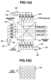
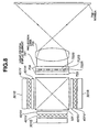
- FIG. 1 (a) is a diagram of the light source device as seen from above;
- Fig. 1 (b) is a plan of a red light source as seen from the side of a dichroic prism serving as a color synthesizing optical system.
- a dichroic prism 101 About the periphery of a dichroic prism 101 are deployed a red light source, a green light source, and a blue light source that are configured from two-dimensional arrays of light emitting diodes (LEDs).
- LEDs light emitting diodes
- the red light source is a structure wherein LEDs 102R (red) that emit light of a wavelength in the red region are fixed to a board 103. Electric power is supplied to the LEDs 102R (red) from a DC power supply 104 via a switch 105 and a variable resistor 106.
- LEDs having a peak light emission wavelength of 620 nm can be used for the LEDs 102R (red). In that case, the color of the emitted light will appear to be orange, but it is assumed that the color orange contains the color red.
- the red light source in this embodiment is configured of an array of a total of 20 LEDs, 5 across and 4 down.
- the LEDs are of a shape formed by molding a transparent resin, the tips whereof have a lens shape, and the diameters whereof are 5 mm or so.
- the number of LEDs depends on the size of the light source needed, and in some applications may be 1.
- the green light source is a structure wherein LEDs 102G (green) that emit light of a wavelength in the green region are fixed to a board 103. Electric power is supplied to the LEDs 102G (green) from a DC power supply 104 via a switch 105 and a variable resistor 106. The number of these LEDs is the same as for the red light source diagrammed in Fig. 1 (b), namely 5 across and 4 down for a total of 20 LEDs.
- LEDs having a peak light emission wavelength of 555 nm can be used for the LEDs 102G (green).
- emitted light that appears yellow-green also contains the green color.
- the blue light source is a structure wherein LEDs 102B (blue) that emit light of a wavelength in the blue region are fixed to a board 103. Electric power is supplied to the LEDs 102B (blue) from a DC power supply 104 via a switch 105 and a variable resistor 106. The number of these LEDs is the same as for the red light source diagrammed in Fig. 1 (b), namely 5 across and 4 down for a total of 20 LEDs.
- LEDs having a peak light emission wavelength of 470 nm can be used for the LEDs 102B (blue).
- the light leaving the red light source is reflected by the red reflecting mirror of the dichroic prism 101.
- the light leaving the blue light source is reflected by the blue reflecting mirror of the dichroic prism 101.
- the light leaving the green light source is transmitted through the dichroic prism 101. In this manner, in the dichroic prism 101, red, green, and blue light from the faces where no light source is deployed is synthesized and output.
- the color of the light synthesized by the dichroic prism 101 can be made white, and hence a white light source can be configured. And by selecting the light source that is lit by the switches 105, light can be emitted in the single colors of red, green, and blue, and hence a single-color light source device can be effected.
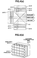
- FIG. 2 (a) is a diagram of the light source device as seen from above;
- Fig. 2 (b) is a plan of a red light source as seen from the dichroic prism side.
- Fig. 2 (b) the LEDs 102R (red) corresponding to lens elements 202R configuring a lens array 201R are described by dotted lines.
- Fig. 2 (a) moreover, the electrical circuitry for the light source, such as is diagrammed in Fig. 1 (a), is not shown.
- red light source Green light source
- blue light source that are configured of two-dimensional arrays of light emitting diodes (LEDs).
- the red light source is configured of an array of LEDs 102R (red) that emit light of a wavelength in the red region, and a lens array 201R deployed between these LEDs and the dichroic prism.
- the lens array 201R is configured by an array of lens elements 202R.
- the aperture shape in the lens elements 202R is rectangular.
- One lens element 202R corresponds with one LED 102R (red), and functions to collimate divergent light that is emitted from the LED and to input light exhibiting high parallelism to the dichroic prism.
- the lens elements 202R in the red light source are designed so that there will be little aberration at the peak light emission wavelength of the LEDs 102R (red).
- an anti-reflective film is formed [thereon] so that reflection at the surface is minimized at that wavelength.
- the green light source is configured of an array of LEDs 102G (green) that emit light of a wavelength in the green region, and a lens array 201G deployed between these LEDs and the dichroic prism.
- the lens array 201G is configured by an array of lens elements (not shown) as in the case of the red light source diagrammed in Fig. 2 (b).
- the lens elements in the green light source are designed so that there will be little aberration at the peak light emission wavelength of the LEDs 102G (green).
- an anti-reflective film is formed [thereon] so that reflection at the surface is minimized at that wavelength.
- the blue light source is configured of an array of LEDs 102B (blue) that emit light of a wavelength in the blue region, and a lens array 201B deployed between these LEDs and the dichroic prism.
- the lens array 201B is configured by an array of lens elements (not shown) as in the case of the red light source diagrammed in Fig. 2 (b).
- the lens elements in the blue light source are designed so that there will be little aberration at the peak light emission wavelength of the LEDs 102B (blue).
- an anti-reflective film is formed [thereon] so that reflection at the surface is minimized at that wavelength.
- the divergent light emitted from the LEDs of the various colors is converted by the lens arrays to light exhibiting high parallelism and input to the dichroic prism, wherefore the light synthesized by the dichroic prism exhibits high parallelism, and a light source device can be provided wherewith the emitted light exhibits high parallelism.
- the shapes of the LEDs are represented as shapes formed by molding a transparent resin so that the tips thereof are lens shaped, but such a lens shape is not always necessary.
- FIG. 3 is a diagram of the light source device as seen from above.
- a flat-panel fluorescent tube 301R (red) emitting light of a wavelength in the red region
- a flat-panel fluorescent tube 301G (green) emitting light of a wavelength in the green region
- a flat-panel fluorescent tube 301B blue
- These fluorescent tubes 301R, 301G, and 301B of the various colors comprise light emitting bodies that, respectively, are a fluorescent body that emits light which is red, a fluorescent body that emits light which is green, and a fluorescent body that emits light which is blue.
- Each of these fluorescent tubes has a planar size such that the light emission area is on the order of 19 mm ⁇ 14 mm.
- the size of the fluorescent tubes is not limited to this size, and may be altered according to the size of the light source required.
- the flat-panel fluorescent tubes 301R, 301G, and 301B as light sources, moreover, light can be emitted uniformly over the prescribed surface area (based on a set value which is according to the size of the area that is to be illuminated in the illuminated body that is to be illuminated), and lens arrays or the like, such as are added when LEDs 102R, 102G, and 102B are used, as in the light source device in the second embodiment, become unnecessary.
- lens arrays or the like such as are added when LEDs 102R, 102G, and 102B are used, as in the light source device in the second embodiment
- rod-shaped fluorescent tubes may be used, deploying such rod-shaped fluorescent tubes in parallel.
- FIG. 4 (a) is a diagram of the light source device as seen from above;
- Fig. 4(b) is a diagonal view of a red light source.
- a flat-panel fluorescent tube 301R (red) emitting light of a wavelength in the red region
- a flat-panel fluorescent tube 301G (green) emitting light of a wavelength in the green region
- a flat-panel fluorescent tube 301B blue
- each prism array 401V and 401H is configured of rows of roof-shaped prisms extending in one direction.
- the prism array 401V and the prism array 401H are deployed so that the directions of the respective prisms are mutually perpendicular.
- light leaving the flat-panel fluorescent tubes is input as divergent light to the dichroic prism.
- the prism arrays in front of the fluorescent tubes, light can be gathered in the normal direction of the fluorescent tubes, and thus a light source device can be configured that exhibits high brightness in the frontal direction.
- the direction of polarization of the light emitted from the flat-panel fluorescent tubes 301R, 301G, and 301B can be aligned.
- the light emitted from the dichroic prism 101 can be made linearly polarized light wherein the direction of oscillation is aligned.
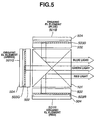
- FIG. 5 is a diagram of the light source device as seen from above.
- an organic electroluminescent element (EL) 501R red
- an organic electroluminescent element (EL) 501G green
- an organic electroluminescent element (EL) 501B blue
- EL organic electroluminescent element
- Each of these organic electroluminescent elements 501R, 501G, and 501B comprises a light emitting layer structure 503R, 503G, and 503B wherein are laminated, on a glass substrate 502, a transparent electrode, an organic thin film layer structure, and a metal electrode.
- the light emitting layer structures are sealed by a sealing substrate 504.
- the organic light emitting layers in the organic thin film layer structures emit light when acted on by a DC electric field applied between the transparent electrodes and the metal thin films.
- a red light source by using a material, that emits light of a red color
- a green light source by using a material that emits light of a green color
- a blue light source by using a material that emits light of a blue color.
- the organic light emitting film for each color has a planar size such that the light emission area is on the order of 19 mm ⁇ 14 mm.
- the size of the light emission area is not limited to this size, but may be altered according to the size of the light source required.
- organic EL elements 501R, 501G, and 501B a superiority is realized in that more uniform light emission can be effected over a certain surface area as compared to when the LEDs 102R, 102G, and 102B are employed as light sources as described earlier (in the light source device in the first embodiment, for example).
- These organic EL elements 501R, 501G, and 501B are similar to the flat-panel fluorescent tubes 301R, 301G, and 301B employed in the light source device in the fourth embodiment described earlier, and are categorized as planar light sources having a single, substantially continuous light emission area.
- FIG. 6 is a diagram of the light source device as seen from above.
- an organic electroluminescent element (EL) 601R red
- an organic electroluminescent element (EL) 601G green
- an organic electroluminescent element (EL) 601B blue
- Each of these organic electroluminescent elements 601R, 601G, and 601B comprises a light emitting layer structure 603R, 603G, and 603B wherein are laminated, on a glass substrate 602, a transparent electrode, an organic thin film layer structure, and a metal electrode.
- the light emitting layer structures are sealed by a sealing substrate 604.
- the organic light emitting layers in the organic thin film layer structures emit light when acted on by a DC electric field applied between the transparent electrodes and the metal thin films.
- a red light source by using a material that emits light of a red color
- a green light source by using a material that emits light of a green color
- a blue light source by using a material that emits light of a blue color.
- the organic light emitting film for each color has a planar size such that the light emission area is on the order of 19 mm ⁇ 14 mm.
- the size of the light emission area is not limited to this size, but may be altered according to the size of the light source required.
- the basic configuration in this embodiment is the same as that of the light source device diagrammed in Fig. 5 in the fifth embodiment.
- the organic thin film layer structure therein is different, however, in that, in this sixth embodiment, an optical resonator structure is comprised in the organic thin film layer structure.
- the optical resonator structure With the optical resonator structure, the spectrum width of the light emitted by the organic EL elements 601R, 601G, and 601B can be narrowed and the color purity thereof enhanced, while the brightness in the normal direction (frontal direction) of the organic EL elements can also be enhanced.
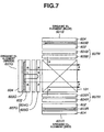
- a seventh embodiment of the light source device of the present invention is described on the basis of Fig. 7.
- the same symbols are used here to designate the same configuring parts of the light source device as in the sixth embodiment.
- the light sources employed in this seventh embodiment are planar light sources, specifically an organic EL element 601R that emits light of a red color, an organic EL element 601G that emits light of a green color, and an organic EL element 601B that emits light of a blue color.
- Each of these light emitting elements 601R, 601G, and 601B comprises an optical resonator structure as in the light source device in the sixth embodiment.
- the light from the light emitting elements 601R, 601G, and 601B of these three colors is synthesized by the dichroic prism 101.
- polarization converter elements 607R, 607G, and 607B configured of quarter-wave films (1/4 ⁇ plates) 604R, 604G, and 604B and reflecting polarizing plates 605R, 605G, and 605B are deployed between the dichroic prism 101 and the light emitting elements 601R, 601G, and 601B.
- the quarter-wave film 604R and the reflecting polarizing plates 605R are deployed in front of the organic EL element 601R emitting light that is red
- the quarter-wave film 604G and the reflecting polarizing plate 605G are deployed in front of the organic EL element 601G emitting light that is green
- the quarter-wave film 604B and the reflecting polarizing plate 605B are deployed in front of the organic EL element 601B emitting light that is blue.
- the reflecting polarizing plates 605R, 605G, and 605B respectively, function to transmit linearly polarized light oscillating in a first direction, and to reflect linearly polarizing light oscillating in a second direction that is perpendicular to the first direction.
- the functions of the polarization converter elements 607R, 607G, and 607B are now described, taking the organic EL element 601G that emits light of a green color as an example.
- the s-polarized light is reflected by the reflecting polarizing plate 605G, converted back to left-handed circularly polarized light by the quarter-wave film 604G, and returned to the organic EL element 601G.
- the left-handed circularly polarized light that is returned to the organic EL element 601G is converted to right-handed circularly polarized light when it is reflected by the cathode electrode of the organic EL element, etc., and then converted to p-polarized light by the quarter-wave film 604G.
- the light emitted from the organic EL element 601G is converted to linearly polarized light, wherein the direction of polarization is aligned, by the polarization converter element 607G configured of the quarter-wave film 604G and the reflecting polarizing plate 605G.
- the quarter-wave film 604G and the reflecting polarizing plate 605G may also be elements that function only in the green wavelength band, or they may be elements that function across the visible light wavelength region that includes red, green, and blue.
- the light emitted from the organic EL element 601R that emits light that is red and the organic EL element 601B that emits light that is blue, similarly, are converted to linearly polarized light P, wherein the direction of oscillation is aligned, by the polarization converter elements 607R and 607B.
- the quarter-wave film 604R and the reflecting polarizing plate 605R corresponding to the red color, or the quarter-wave film 604B and the reflecting polarizing plate 605B corresponding to the blue color may be elements that, respectively, function only in the red or blue wavelength bands, or they may be elements that function across the visible light wavelength region that includes red, green, and blue.
- the red, green, and blue light that has become linearly polarized light is synthesized by the dichroic prism 101 and output from the dichroic prism 101 as linearly polarized light wherein the direction of oscillation is aligned.
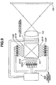
- Fig. 8 is a diagram of the main optical system of the display device, as seen from above.
- the light source device On the back side of a liquid crystal display element 701 is deployed the light source device described in the fourth embodiment as the light source diagrammed in Fig. 4.
- the light source device is configured of a dichroic prism 101, flat-panel fluorescent tube 301R (red), flat-panel fluorescent tube 301G (green), flat-panel fluorescent tube 301B (blue), and prism arrays 401V and 401H.
- White light resulting from the synthesis of red, green, and blue colors is directed onto the liquid crystal display element 701.
- the image displayed on the liquid crystal display element 701 is magnified and projected onto a screen 706 by a projection lens 705.
- the liquid crystal display element 101 has a liquid crystal layer 703 that is sandwiched between glass substrates 704, whereon are formed color filters 702R, 702G, and 702B, in each pixel, for displaying color images. To make it easier to understand, this diagram is drawn without showing the wiring or elements that drive the liquid crystal.
- the display area on the liquid crystal display element 701 is 18.3 ⁇ 13.7 mm (0.9 inch diagonally), for example.
- the size of this display area can be altered as necessary, but the sizes of the light emission areas of the light sources for each color must also be altered to match the size of the display area.
- reflecting polarizing plates may be deployed between the dichroic prism and the prism arrays.
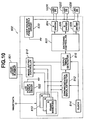
- FIG. 9 is a diagram of the main optical system of the display device, as seen from above;
- Fig. 10 is a detailed block diagram of the control circuit in the display device; and
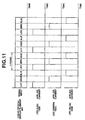
- Fig. 11 is a timing chart for the timing of light source lighting and liquid crystal display element displaying.
- the light source device is configured of a dichroic prism 101, LED 102R (red), LED 102G (green), LED 102B (blue), and lens arrays 201R, 201G, and 201B.
- the lighting of the LEDs of each color and the driving of the liquid crystal display element are controlled by a display controller circuit 802.
- FIG. 10 a detailed diagram of the display controller circuit 802 is given.
- This display controller circuit 802 is provided with frame memories 810 corresponding to each color R, G, and B.
- Image data are temporarily stored in the frame memories 810 of each respective color.
- synchronization signals are extracted by a synchronization signal extractor unit 812, and synchronization is effected by clock signals from a clock 814.
- the configuration is such that the synchronization signals are output to an output timing generator 816, and output both to an image output controller 818 which controls the driving of the liquid crystal display element 801 and to a switching controller 820 that controls the driving of the light emitting elements of each color.
- To the image output controller 818 are input image data from the frame memories 810, and prescribed images are formed on the liquid crystal display element 801 by power supplied from an LCD (liquid crystal device) power supply circuit 822, based on the synchronization signals noted above.
- LCD liquid crystal device
- the switching controller 820 in order to light the light emitting elements of colors corresponding to the images displayed by the liquid crystal display element 801, signals are sequentially switched and output to an R driver 824, a G driver 826, and a B driver 828.
- an R driver 824 in order to light the light emitting elements of colors corresponding to the images displayed by the liquid crystal display element 801
- signals are sequentially switched and output to an R driver 824, a G driver 826, and a B driver 828.
- the sequential lighting of the LEDs 102R, 102G, and 102B, in an order prescribed by RGB (and in synchronization with the order of image display to the liquid crystal display element 801) is repeated.
- Red-component images, green-component images, and blue-component images are sequentially displayed within one field in the liquid crystal display element 801.
- the timing of LED lighting and of images displayed on the liquid crystal display element is controlled so that while the red-component image is being displayed the red LED 102R is lit, while the green-component image is being displayed the green LED 102G is lit, and while the blue-component image is being displayed the blue LED 102B is lit.
- the liquid crystal display element 701 in the display device of the first embodiment diagrammed in Fig. 8 absorb light of wavelengths other than the respective transmission wavelengths thereof.
- the light utilization efficiency from the light source to the screen can be enhanced.
- the color-sequence display scheme described in the foregoing can be employed instead of using color filters in the liquid crystal display element 701 and the light utilization efficiency enhanced accordingly.
- the light from the RGB light sources is output after passing through the dichroic prism 101, wherefore the light axes of the light sources of the several colors coincide, and the liquid crystal display element can be illuminated by the light sources of the several colors in the same direction, wherefore a benefit is realized in that the color is not dependent on visual angle.
- FIG. 12 is a diagram of the main optical system of the display device, as seen from above.
- a liquid crystal display element 701 On the back side of a liquid crystal display element 701 is deployed the light source device of the first embodiment diagrammed in Fig. 1.
- the light source device is configured of the dichroic prism 101, LED 102R (red), LED 102G (green), and LED 102B (blue), and the liquid crystal display element 701 is illuminated by white light synthesized from the red, green, and blue light.
- the display device in this embodiment is a display device wherewith virtual images are viewed that pass through a lens 1001 and are magnified by the liquid crystal display element 701.
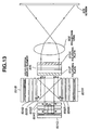
- a fourth embodiment of the display device of the present invention is described on the basis of Fig. 13.
- a liquid crystal display device 606 On the back side of a liquid crystal display device 606 is deployed the light source device described in the seventh embodiment as the light source device diagrammed in Fig. 7.
- the light source device consists of the organic EL elements 601R, 601G, and 601B that comprise an optical resonator structure.
- On the front side of the organic EL elements 601R 601G, and 601B are deployed the quarter-wave films 604R, 604G, and 604B and the reflecting polarizing plates 605R, 605G, and 605B.
- light output from the dichroic prism 101 is linearly polarized light P wherein the direction of oscillation is aligned.
- the liquid crystal display element 606 is provided with an input-side polarizing plate 610P and an output-side polarizing plate 610A.
- an input-side polarizing plate 610P aligns with the direction of oscillation in the linearly polarized light P, the absorption of light by the polarizing plate 610P can be reduced, the light quantity that can be transmitted through the liquid crystal display element 606 can be increased, and the light from the light source device can be efficiently modulated by the liquid crystal display element 606.
- the images displayed on the liquid crystal display element 606 are magnified and projected onto a screen 609 by a projection lens 608.
- color images can be projected by simultaneously lighting the red, green, and blue organic EL elements 601R, 601G, and 601B, and illuminating the liquid crystal display element with white light.
- color image displays can be made by employing a color-sequence drive for lighting the red, green, and blue EL elements 601R, 601G, and 601B, such as described in the second embodiment of the display device, in order, in one frame.
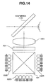
- FIG. 14 is a diagram of the main optical system of the display device, as seen from above.
- the display device diagrammed in Fig. 14 has the same light source device and liquid crystal display device configuration as diagrammed in Fig. 13, with the only difference being the deployment of a half mirror 1101 between a lens 1001 and the eye 1002 of an observer.
- the half mirror 1101 enables magnified images of the liquid crystal display element 701 to be viewed superimposed on the outside world 1102.
- a fully reflecting mirror may be used in place of the half mirror.
- the light sources employed for effecting color-sequence drive in the embodiment aspects, particularly in the embodiment aspects of the display device, are not limited to point light sources like LEDs, but may be planar light sources such as organic EL elements or flat-panel fluorescent tubes, etc.
- transmissive type liquid crystal display elements are used.
- the present invention is not limited thereto or thereby, however, and optical devices are also provided by the present invention wherein reflective type liquid crystal display elements that reflect light from a light source, or light valves wherewith images are formed using a deformable mirror, or light modulating devices of a type that reflect light from the outside, such as spatial modulation elements, etc., are combined as light modulating members or means together with light sources.
- a benefit is realized in that a small light source device can be configured wherewith bright white light can be generated.
- a benefit is realized in that a small display device can be configured. Furthermore, by lighting the light sources for red, green, and blue light in order, and causing, in synchronization therewith, red-, green-, and blue-component images to be displayed on the liquid crystal display element or other light modulating element, a benefit is realized in that the brightness of a small display device comprising a single light modulating element can be enhanced.
Applications Claiming Priority (3)
| Application Number | Priority Date | Filing Date | Title |
|---|---|---|---|
| JP15762198 | 1998-06-05 | ||
| JP15762198 | 1998-06-05 | ||
| PCT/JP1999/003011 WO1999064912A1 (fr) | 1998-06-05 | 1999-06-04 | Source lumineuse et dispositif d'affichage |
Publications (3)
| Publication Number | Publication Date |
|---|---|
| EP1003062A1 true EP1003062A1 (de) | 2000-05-24 |
| EP1003062A4 EP1003062A4 (de) | 2002-01-09 |
| EP1003062B1 EP1003062B1 (de) | 2006-11-08 |
Family
ID=15653742
Family Applications (1)
| Application Number | Title | Priority Date | Filing Date |
|---|---|---|---|
| EP99923922A Expired - Lifetime EP1003062B1 (de) | 1998-06-05 | 1999-06-04 | Lichtquelle und anzeigevorrichtung |
Country Status (7)
| Country | Link |
|---|---|
| US (2) | US6882379B1 (de) |
| EP (1) | EP1003062B1 (de) |
| KR (1) | KR100792603B1 (de) |
| CN (1) | CN100390599C (de) |
| AT (1) | ATE344936T1 (de) |
| DE (1) | DE69933917T2 (de) |
| WO (1) | WO1999064912A1 (de) |
Cited By (21)
| Publication number | Priority date | Publication date | Assignee | Title |
|---|---|---|---|---|
| WO2004059608A1 (ja) * | 2002-12-26 | 2004-07-15 | Sanyo Electric Co., Ltd. | 投写型映像表示装置 |
| WO2004097946A2 (de) * | 2003-04-29 | 2004-11-11 | Osram Opto Semiconductors Gmbh | Lichtquelle |
| EP1616219A2 (de) * | 2003-04-24 | 2006-01-18 | Chromnomotion Imaging Applications, Inc. | Röhrenloses optisches licht-engine-system |
| WO2006059272A1 (en) * | 2004-11-30 | 2006-06-08 | Koninklijke Philips Electronics N.V. | Miniaturized projection display |
| EP1640313A3 (de) * | 2004-09-27 | 2007-03-07 | Idc, Llc | Vorrichtung und Verfahren zum Verringern der wahrgenommenen Farbverschiebung |
| WO2007025525A2 (de) | 2005-08-31 | 2007-03-08 | Osram Opto Semiconductors Gmbh | Lichtemittierendes modul insbesondere zur verwendung in einem optischen projektionsgerät und optisches projektionsgerät |
| US8138479B2 (en) | 2009-01-23 | 2012-03-20 | Qualcomm Mems Technologies, Inc. | Integrated light emitting and light detecting device |
| EP2592472A1 (de) * | 2010-07-06 | 2013-05-15 | Seiko Epson Corporation | Lichtquellenvorrichtung und projektor |
| US8798425B2 (en) | 2007-12-07 | 2014-08-05 | Qualcomm Mems Technologies, Inc. | Decoupled holographic film and diffuser |
| US8848294B2 (en) | 2010-05-20 | 2014-09-30 | Qualcomm Mems Technologies, Inc. | Method and structure capable of changing color saturation |
| US8872085B2 (en) | 2006-10-06 | 2014-10-28 | Qualcomm Mems Technologies, Inc. | Display device having front illuminator with turning features |
| US8928967B2 (en) | 1998-04-08 | 2015-01-06 | Qualcomm Mems Technologies, Inc. | Method and device for modulating light |
| US8971675B2 (en) | 2006-01-13 | 2015-03-03 | Qualcomm Mems Technologies, Inc. | Interconnect structure for MEMS device |
| US8979349B2 (en) | 2009-05-29 | 2015-03-17 | Qualcomm Mems Technologies, Inc. | Illumination devices and methods of fabrication thereof |
| US9019183B2 (en) | 2006-10-06 | 2015-04-28 | Qualcomm Mems Technologies, Inc. | Optical loss structure integrated in an illumination apparatus |
| US9019590B2 (en) | 2004-02-03 | 2015-04-28 | Qualcomm Mems Technologies, Inc. | Spatial light modulator with integrated optical compensation structure |
| US9025235B2 (en) | 2002-12-25 | 2015-05-05 | Qualcomm Mems Technologies, Inc. | Optical interference type of color display having optical diffusion layer between substrate and electrode |
| EP2472315A4 (de) * | 2009-08-25 | 2015-06-17 | Mitsubishi Electric Corp | Optisches lichtsammelsystem und projektionsbildanzeigevorrichtung |
| US9110289B2 (en) | 1998-04-08 | 2015-08-18 | Qualcomm Mems Technologies, Inc. | Device for modulating light with multiple electrodes |
| CN105122450A (zh) * | 2013-04-22 | 2015-12-02 | 欧司朗光电半导体有限公司 | 光学装置和显示设备 |
| US9244212B2 (en) | 2008-01-30 | 2016-01-26 | Qualcomm Mems Technologies, Inc. | Illumination device having a tapered light guide |
Families Citing this family (112)
| Publication number | Priority date | Publication date | Assignee | Title |
|---|---|---|---|---|
| US6674562B1 (en) | 1994-05-05 | 2004-01-06 | Iridigm Display Corporation | Interferometric modulation of radiation |
| DE19751716C2 (de) * | 1996-11-25 | 2002-06-20 | Fraunhofer Ges Forschung | Anordnung zur Formung und Führung von Strahlung |
| DE19949198B4 (de) | 1999-10-13 | 2005-04-14 | Myos My Optical Systems Gmbh | Vorrichtung mit mindestens einer mehrere Einzel-Lichtquellen umfassenden Lichtquelle |
| US7710669B2 (en) | 2000-08-24 | 2010-05-04 | Wavien, Inc. | Etendue efficient combination of multiple light sources |
| CN100423532C (zh) * | 2001-08-09 | 2008-10-01 | 松下电器产业株式会社 | 图像读取装置的光源以及光源的驱动装置 |
| CN100407752C (zh) * | 2001-08-09 | 2008-07-30 | 松下电器产业株式会社 | 图像读取装置的光源以及光源的驱动装置 |
| KR100440958B1 (ko) * | 2001-10-12 | 2004-07-21 | 삼성전자주식회사 | 조명계 및 이를 채용한 프로젝터 |
| KR100440959B1 (ko) | 2001-11-08 | 2004-07-21 | 삼성전자주식회사 | 조명계 및 이를 채용한 프로젝션 시스템 |
| KR100464207B1 (ko) * | 2001-12-17 | 2005-01-03 | 엘지.필립스 엘시디 주식회사 | 반사형 필드순차구동 액정표시소자 |
| CN100443955C (zh) * | 2002-01-23 | 2008-12-17 | 深圳Tcl新技术有限公司 | 非相干光全谱域调制方法及其视频投影光机 |
| KR20030090021A (ko) * | 2002-05-20 | 2003-11-28 | 삼성전기주식회사 | 반사형 평판 편광판을 이용한 프로젝션 시스템 |
| US6896381B2 (en) * | 2002-10-11 | 2005-05-24 | Light Prescriptions Innovators, Llc | Compact folded-optics illumination lens |
| JP3866651B2 (ja) * | 2002-12-02 | 2007-01-10 | Necビューテクノロジー株式会社 | 投写型表示装置 |
| US7377671B2 (en) * | 2003-02-04 | 2008-05-27 | Light Prescriptions Innovators, Llc | Etendue-squeezing illumination optics |
| JP3858850B2 (ja) * | 2003-05-06 | 2006-12-20 | セイコーエプソン株式会社 | 表示装置、及び表示方法、並びにプロジェクタ |
| US7329029B2 (en) * | 2003-05-13 | 2008-02-12 | Light Prescriptions Innovators, Llc | Optical device for LED-based lamp |
| US8075147B2 (en) * | 2003-05-13 | 2011-12-13 | Light Prescriptions Innovators, Llc | Optical device for LED-based lamp |
| JP2005003900A (ja) * | 2003-06-11 | 2005-01-06 | Seiko Epson Corp | プロジェクタ |
| JP2005037503A (ja) * | 2003-07-16 | 2005-02-10 | Seiko Epson Corp | 空間光変調装置及びプロジェクタ |
| CN100356269C (zh) * | 2003-10-22 | 2007-12-19 | 联华电子股份有限公司 | 发光二极管照明装置 |
| US7144121B2 (en) * | 2003-11-14 | 2006-12-05 | Light Prescriptions Innovators, Llc | Dichroic beam combiner utilizing blue LED with green phosphor |
| JP2005157059A (ja) * | 2003-11-27 | 2005-06-16 | Seiko Epson Corp | 照明装置及びプロジェクタ |
| DE10359753B3 (de) * | 2003-12-19 | 2005-08-18 | Carl Zeiss Jena Gmbh | Anordnung zum Beleuchten eines Displays |
| US7855824B2 (en) | 2004-03-06 | 2010-12-21 | Qualcomm Mems Technologies, Inc. | Method and system for color optimization in a display |
| JP4096896B2 (ja) * | 2004-03-10 | 2008-06-04 | セイコーエプソン株式会社 | プロジェクタ |
| US7408527B2 (en) * | 2004-04-30 | 2008-08-05 | Infocus Corporation | Light emitting device driving method and projection apparatus so equipped |
| US7083284B2 (en) * | 2004-04-30 | 2006-08-01 | Infocus Corporation | Method and apparatus for sequencing light emitting devices in projection systems |
| US20050275762A1 (en) * | 2004-06-09 | 2005-12-15 | United Microelectronics Corp. | Liquid crystal on silicon display device |
| KR100619043B1 (ko) | 2004-08-03 | 2006-09-01 | 삼성전자주식회사 | 조명유니트 및 이를 채용한 화상투사장치 |
| DE102004045911B4 (de) | 2004-09-20 | 2007-08-02 | My Optical Systems Gmbh | Vorrichtung zur Überlagerung von Strahlenbündeln |
| DE102004045912B4 (de) | 2004-09-20 | 2007-08-23 | My Optical Systems Gmbh | Verfahren und Vorrichtung zur Überlagerung von Strahlenbündeln |
| DE102004045914B4 (de) | 2004-09-20 | 2008-03-27 | My Optical Systems Gmbh | Verfahren und Vorrichtung zur Überlagerung von Strahlenbündeln |
| US7898521B2 (en) | 2004-09-27 | 2011-03-01 | Qualcomm Mems Technologies, Inc. | Device and method for wavelength filtering |
| US7710632B2 (en) | 2004-09-27 | 2010-05-04 | Qualcomm Mems Technologies, Inc. | Display device having an array of spatial light modulators with integrated color filters |
| US7911428B2 (en) | 2004-09-27 | 2011-03-22 | Qualcomm Mems Technologies, Inc. | Method and device for manipulating color in a display |
| US8362987B2 (en) | 2004-09-27 | 2013-01-29 | Qualcomm Mems Technologies, Inc. | Method and device for manipulating color in a display |
| US7807488B2 (en) | 2004-09-27 | 2010-10-05 | Qualcomm Mems Technologies, Inc. | Display element having filter material diffused in a substrate of the display element |
| JP4186918B2 (ja) * | 2004-12-01 | 2008-11-26 | セイコーエプソン株式会社 | 画像表示装置 |
| CN101248384B (zh) * | 2005-02-09 | 2013-04-10 | 微阳有限公司 | 多光源光束扩展量的有效组合 |
| US7316497B2 (en) * | 2005-03-29 | 2008-01-08 | 3M Innovative Properties Company | Fluorescent volume light source |
| US20060227147A1 (en) * | 2005-04-07 | 2006-10-12 | Toon Diels | Method and apparatus for an image presentation device with illumination control for black image processing |
| KR20060111793A (ko) * | 2005-04-25 | 2006-10-30 | 삼성전자주식회사 | 조명유니트 및 이를 채용한 화상투사장치 |
| US7445340B2 (en) | 2005-05-19 | 2008-11-04 | 3M Innovative Properties Company | Polarized, LED-based illumination source |
| JP4085395B2 (ja) * | 2005-06-10 | 2008-05-14 | ミネベア株式会社 | 光源装置およびそれを用いた画像表示装置 |
| FR2887640B1 (fr) * | 2005-06-24 | 2008-10-03 | Thomson Licensing Sa | Procede d'illumination d'un imageur de projecteur, systeme et projecteur correspondant |
| JP2009503793A (ja) * | 2005-07-28 | 2009-01-29 | ライト プレスクリプションズ イノベーターズ エルエルシー | バックライトおよびフロントライト用のエテンデュ保存型照明光学部品 |
| EP1920285A4 (de) * | 2005-07-28 | 2010-11-03 | Light Prescriptions Innovators | Linsenförmige optische freiformelemente und ihre anwendung auf kondensatoren und scheinwerfer |
| US8631787B2 (en) * | 2005-07-28 | 2014-01-21 | Light Prescriptions Innovators, Llc | Multi-junction solar cells with a homogenizer system and coupled non-imaging light concentrator |
| WO2007015389A1 (ja) * | 2005-08-04 | 2007-02-08 | Matsushita Electric Industrial Co., Ltd. | 照明装置及びそれを用いた投写型表示装置 |
| US7434940B2 (en) * | 2005-09-06 | 2008-10-14 | Hewlett-Packard Development Company, L.P. | Light coupling system and method |
| US20070097066A1 (en) * | 2005-10-27 | 2007-05-03 | Ward Calvin B | LCD display utilizing light emitters with variable light output |
| US7540616B2 (en) * | 2005-12-23 | 2009-06-02 | 3M Innovative Properties Company | Polarized, multicolor LED-based illumination source |
| KR100772398B1 (ko) * | 2006-02-25 | 2007-11-01 | 삼성전자주식회사 | 2스캔의 광원 및 이를 이용한 영상장치 및 그 구동방법 |
| US8004743B2 (en) | 2006-04-21 | 2011-08-23 | Qualcomm Mems Technologies, Inc. | Method and apparatus for providing brightness control in an interferometric modulator (IMOD) display |
| US7846391B2 (en) | 2006-05-22 | 2010-12-07 | Lumencor, Inc. | Bioanalytical instrumentation using a light source subsystem |
| US20070279914A1 (en) * | 2006-06-02 | 2007-12-06 | 3M Innovative Properties Company | Fluorescent volume light source with reflector |
| US20070280622A1 (en) * | 2006-06-02 | 2007-12-06 | 3M Innovative Properties Company | Fluorescent light source having light recycling means |
| EP2064487A4 (de) * | 2006-07-14 | 2010-09-01 | Light Prescriptions Innovators | Helligkeitsverstärkender film |
| EP2057409A2 (de) * | 2006-08-10 | 2009-05-13 | Light Prescriptions Innovators, LLC. | Rezyklierung von led-licht für helligkeitsverstärkung und winkelverengung |
| WO2008022065A2 (en) * | 2006-08-11 | 2008-02-21 | Light Prescriptions Innovators, Llc | Led luminance-enhancement and color-mixing by rotationally multiplexed beam-combining |
| JP4239107B2 (ja) * | 2006-08-25 | 2009-03-18 | カシオ計算機株式会社 | 光源装置及びプロジェクタ |
| US7857457B2 (en) * | 2006-09-29 | 2010-12-28 | 3M Innovative Properties Company | Fluorescent volume light source having multiple fluorescent species |
| US20080231953A1 (en) * | 2007-03-22 | 2008-09-25 | Young Garrett J | System and Method for LED Polarization Recycling |
| US8098375B2 (en) | 2007-08-06 | 2012-01-17 | Lumencor, Inc. | Light emitting diode illumination system |
| EP2232569A2 (de) | 2007-12-17 | 2010-09-29 | QUALCOMM MEMS Technologies, Inc. | PHOTOVOLTAIsche Elemente mit INTERFEROMETRIschen Rückseitenmasken |
| US8104945B2 (en) * | 2007-12-27 | 2012-01-31 | Samsung Led Co., Ltd. | Backlight unit implementing local dimming for liquid crystal display device |
| JP2011512006A (ja) | 2008-01-30 | 2011-04-14 | デジタル オプティクス インターナショナル,リミティド ライアビリティ カンパニー | 薄型照明システム |
| US9151884B2 (en) * | 2008-02-01 | 2015-10-06 | 3M Innovative Properties Company | Fluorescent volume light source with active chromphore |
| JP5245588B2 (ja) * | 2008-07-10 | 2013-07-24 | ソニー株式会社 | プロジェクタ装置およびプロジェクタ装置用の画像合成装置 |
| TW201017863A (en) * | 2008-10-03 | 2010-05-01 | Versitech Ltd | Semiconductor color-tunable broadband light sources and full-color microdisplays |
| EP2350526B1 (de) | 2008-10-10 | 2014-12-31 | Qualcomm Mems Technologies, Inc | Verteiltes beleuchtungssystem |
| CN101725932B (zh) * | 2008-10-30 | 2011-08-24 | 鸿富锦精密工业(深圳)有限公司 | 光源模组及使用该光源模组的投影机 |
| KR101543467B1 (ko) | 2008-11-13 | 2015-08-10 | 엘지전자 주식회사 | 프로젝션 시스템 |
| CN102272516A (zh) | 2009-01-13 | 2011-12-07 | 高通Mems科技公司 | 大面积光面板及屏幕 |
| US8242462B2 (en) | 2009-01-23 | 2012-08-14 | Lumencor, Inc. | Lighting design of high quality biomedical devices |
| CN201568808U (zh) * | 2009-07-31 | 2010-09-01 | 深圳市光峰光电技术有限公司 | 高效合光的舞台灯光照明装置 |
| US8536789B2 (en) | 2010-01-04 | 2013-09-17 | Volkswagen Ag | Head light for a motor vehicle |
| US8402647B2 (en) | 2010-08-25 | 2013-03-26 | Qualcomm Mems Technologies Inc. | Methods of manufacturing illumination systems |
| CN102455512B (zh) | 2010-10-21 | 2014-03-12 | 中强光电股份有限公司 | 照明装置及投影装置 |
| CN102063001A (zh) * | 2010-11-19 | 2011-05-18 | 封燕鸣 | 固体光源单系统分时彩色投影机及投影方法 |
| US8389957B2 (en) | 2011-01-14 | 2013-03-05 | Lumencor, Inc. | System and method for metered dosage illumination in a bioanalysis or other system |
| US8466436B2 (en) | 2011-01-14 | 2013-06-18 | Lumencor, Inc. | System and method for metered dosage illumination in a bioanalysis or other system |
| US8393737B2 (en) * | 2011-03-03 | 2013-03-12 | Ford Global Technologies, Llc | Light engine using common building blocks |
| KR101753587B1 (ko) * | 2011-03-28 | 2017-07-19 | 엘지전자 주식회사 | 이동 단말기 |
| TWI446002B (zh) * | 2011-04-29 | 2014-07-21 | Delta Electronics Inc | 光源裝置 |
| JP5643720B2 (ja) * | 2011-06-30 | 2014-12-17 | 株式会社沖データ | ディスプレイモジュール及びその製造方法と表示装置 |
| US20130002926A1 (en) * | 2011-06-30 | 2013-01-03 | SmallHD, LLC | Portable Video Viewing Device |
| WO2013011427A1 (en) * | 2011-07-15 | 2013-01-24 | Koninklijke Philips Electronics N.V. | Luminaire emitting light of different colours |
| US8967846B2 (en) | 2012-01-20 | 2015-03-03 | Lumencor, Inc. | Solid state continuous white light source |
| CN103424969B (zh) * | 2012-05-21 | 2015-08-19 | 台达电子工业股份有限公司 | 光源系统 |
| US9217561B2 (en) | 2012-06-15 | 2015-12-22 | Lumencor, Inc. | Solid state light source for photocuring |
| DE102012105487A1 (de) * | 2012-06-22 | 2014-01-23 | Seereal Technologies S.A. | Lichtmodulator mit einem schaltbaren Volumengitter |
| JP5682692B2 (ja) | 2012-12-21 | 2015-03-11 | 株式会社リコー | 画像表示装置 |
| EP2998641B1 (de) * | 2013-05-17 | 2023-07-05 | YLX Incorporated | Lichtemittierende vorrichtung und bühnenlampensystem |
| KR20150012520A (ko) | 2013-07-25 | 2015-02-04 | 삼성디스플레이 주식회사 | 표시 장치 및 이의 제조 방법 |
| US9743053B2 (en) | 2013-10-17 | 2017-08-22 | Sony Corporation | Light source apparatus and image display apparatus |
| CN104297927A (zh) * | 2014-09-29 | 2015-01-21 | 四川长虹电器股份有限公司 | 一种激光二极管阵列光源模组 |
| CN110579884B (zh) * | 2014-10-31 | 2022-06-21 | 深圳光峰科技股份有限公司 | 发光装置及具有其的投影仪 |
| CN204964979U (zh) * | 2015-09-22 | 2016-01-13 | 广景视睿科技(深圳)有限公司 | 一种投影照明光路 |
| US11275237B2 (en) * | 2017-04-05 | 2022-03-15 | Osram Oled Gmbh | Apparatus for presenting an image |
| JP6965580B2 (ja) * | 2017-06-01 | 2021-11-10 | セイコーエプソン株式会社 | 表示装置 |
| CN109681790A (zh) * | 2017-10-18 | 2019-04-26 | 深圳市绎立锐光科技开发有限公司 | 光源系统及照明设备 |
| JP7067185B2 (ja) * | 2018-03-27 | 2022-05-16 | セイコーエプソン株式会社 | 表示装置 |
| JP6922813B2 (ja) | 2018-03-27 | 2021-08-18 | セイコーエプソン株式会社 | 光学ユニット、および表示装置 |
| JP7081256B2 (ja) * | 2018-03-27 | 2022-06-07 | セイコーエプソン株式会社 | 光学ユニット、および表示装置 |
| CN110632814A (zh) | 2018-06-25 | 2019-12-31 | 中强光电股份有限公司 | 照明系统以及投影装置 |
| JP6939727B2 (ja) * | 2018-07-18 | 2021-09-22 | セイコーエプソン株式会社 | 画像表示モジュールおよび画像表示装置 |
| WO2020086156A1 (en) * | 2018-08-31 | 2020-04-30 | Congliang Chen | Microscope with led illumination assembly |
| JP6947143B2 (ja) * | 2018-09-19 | 2021-10-13 | セイコーエプソン株式会社 | 画像表示モジュールおよび画像表示装置 |
| JP6958530B2 (ja) * | 2018-10-10 | 2021-11-02 | セイコーエプソン株式会社 | 光学モジュールおよび頭部装着型表示装置 |
| CN113543747A (zh) * | 2019-03-08 | 2021-10-22 | 皇家飞利浦有限公司 | 用于口腔护理器具的基于纤维的灯环 |
| CN209590522U (zh) | 2019-04-16 | 2019-11-05 | 中强光电股份有限公司 | 照明系统及投影装置 |
Citations (10)
| Publication number | Priority date | Publication date | Assignee | Title |
|---|---|---|---|---|
| US4870268A (en) * | 1986-04-02 | 1989-09-26 | Hewlett-Packard Company | Color combiner and separator and implementations |
| US5438453A (en) * | 1992-07-03 | 1995-08-01 | Rohm Co., Ltd. | Light source for flat-panel display |
| JPH08201757A (ja) * | 1995-01-30 | 1996-08-09 | A G Technol Kk | 投射型カラー表示装置 |
| WO1997014076A1 (en) * | 1995-10-13 | 1997-04-17 | Unic View Ltd. | Projector |
| US5661608A (en) * | 1994-04-12 | 1997-08-26 | Sextant Avionique | Light box for optical valve |
| EP0808071A1 (de) * | 1991-03-19 | 1997-11-19 | Hitachi, Ltd. | Flüssigkristallanzeigevorrichtung und reflektive Flüssigkristallanzeigetafel |
| US5706061A (en) * | 1995-03-31 | 1998-01-06 | Texas Instruments Incorporated | Spatial light image display system with synchronized and modulated light source |
| WO1998013725A1 (fr) * | 1996-09-24 | 1998-04-02 | Seiko Epson Corporation | Ecran de projection a source lumineuse |
| WO1998020475A1 (en) * | 1996-11-01 | 1998-05-14 | Laser Power Corporation | Projection display with gradation levels obtained by modulation of beamlets |
| US5757445A (en) * | 1990-12-31 | 1998-05-26 | Kopin Corporation | Single crystal silicon tiles for display panels |
Family Cites Families (41)
| Publication number | Priority date | Publication date | Assignee | Title |
|---|---|---|---|---|
| US4438453A (en) * | 1982-01-21 | 1984-03-20 | Polaroid Corporation | Constant light greyscale generator for CRT color camera system |
| GB2170940B (en) * | 1984-12-25 | 1989-04-12 | Ricoh Kk | Liquid crystal color display device |
| US4777235A (en) | 1987-07-01 | 1988-10-11 | Amoco Corporation | Production of polyarylene ether from activated dihalo benzenoid monomer, dihydroxy benzenoid monomer and Bis(hydroxyphenyl) monomer |
| JP3128274B2 (ja) | 1990-07-31 | 2001-01-29 | 三洋電機株式会社 | 平面型螢光ランプ及びこれを用いた液晶プロジェクタ |
| EP0588937B1 (de) | 1991-06-13 | 1996-08-28 | Minnesota Mining And Manufacturing Company | Retroreflektierender polarisator |
| JPH05313128A (ja) * | 1992-05-14 | 1993-11-26 | Matsushita Electric Ind Co Ltd | 表示装置とその駆動方法 |
| US5903388A (en) * | 1992-06-11 | 1999-05-11 | Sedlmayr Steven R | High efficiency electromagnetic beam projector and systems and method for implementation thereof |
| US5359345A (en) | 1992-08-05 | 1994-10-25 | Cree Research, Inc. | Shuttered and cycled light emitting diode display and method of producing the same |
| US5561538A (en) * | 1992-11-17 | 1996-10-01 | Sharp Kabushiki Kaisha | Direct-view display apparatus |
| JP3332454B2 (ja) | 1993-02-26 | 2002-10-07 | 三洋電機株式会社 | 平面蛍光ランプ |
| JPH0764079A (ja) | 1993-08-31 | 1995-03-10 | Hitachi Ltd | 投写形液晶表示装置 |
| SE505633C2 (sv) | 1993-10-29 | 1997-09-22 | Lars Lindqvist | Transportlåda för i behållare planterade växter |
| JP3373265B2 (ja) * | 1993-11-04 | 2003-02-04 | 松下電器産業株式会社 | 頭部装着型映像表示装置 |
| US5828488A (en) | 1993-12-21 | 1998-10-27 | Minnesota Mining And Manufacturing Co. | Reflective polarizer display |
| WO1995027919A2 (en) | 1994-04-06 | 1995-10-19 | Minnesota Mining And Manufacturing Company | Polarized light sources |
| US5953114A (en) | 1994-04-11 | 1999-09-14 | Leica Mikroskopie Systeme Ag | Method of determining measurement-point position data and device for measuring the magnification of an optical beam path |
| JP2885093B2 (ja) * | 1994-10-17 | 1999-04-19 | 日本電気株式会社 | 画像表示方法 |
| JPH08140107A (ja) * | 1994-11-11 | 1996-05-31 | Mitsubishi Electric Corp | 投射型画像表示装置 |
| JP3387247B2 (ja) * | 1994-11-30 | 2003-03-17 | 株式会社島津製作所 | 液晶表示器 |
| JP2939860B2 (ja) | 1995-01-24 | 1999-08-25 | カシオ計算機株式会社 | 投影型液晶表示装置 |
| WO1997012276A1 (en) | 1995-09-25 | 1997-04-03 | Philips Electronics N.V. | Electroluminescent illumination system and a flat-panel picture display device provided with such a system |
| JPH09105929A (ja) * | 1995-10-12 | 1997-04-22 | Asahi Glass Co Ltd | 液晶表示装置 |
| JP3528470B2 (ja) | 1995-10-27 | 2004-05-17 | 株式会社豊田中央研究所 | 微小光共振器型有機電界発光素子 |
| US6011602A (en) * | 1995-11-06 | 2000-01-04 | Seiko Epson Corporation | Lighting apparatus with a light guiding body having projections in the shape of a trapezoid |
| JPH09146092A (ja) * | 1995-11-22 | 1997-06-06 | Hitachi Ltd | 照明装置およびそれを用いた液晶表示装置 |
| TW359765B (en) | 1996-05-10 | 1999-06-01 | Seiko Epson Corp | Projection type liquid crystal display apparatus |
| JP3671530B2 (ja) * | 1996-07-11 | 2005-07-13 | セイコーエプソン株式会社 | 液晶表示装置 |
| JP4050802B2 (ja) * | 1996-08-02 | 2008-02-20 | シチズン電子株式会社 | カラー表示装置 |
| JPH1050124A (ja) * | 1996-08-06 | 1998-02-20 | Seiko Epson Corp | 照明装置および液晶表示装置 |
| JPH10123512A (ja) * | 1996-08-28 | 1998-05-15 | Sanyo Electric Co Ltd | 液晶表示装置用光源及びそれを用いたカラー液晶表示装置 |
| JPH10206980A (ja) | 1997-01-27 | 1998-08-07 | Noritsu Koki Co Ltd | プリンタプロセッサー |
| JPH10269802A (ja) | 1997-03-24 | 1998-10-09 | Sony Corp | 照明装置および映像表示装置 |
| JP3941167B2 (ja) | 1997-03-24 | 2007-07-04 | ソニー株式会社 | 映像表示装置及び映像表示方法 |
| JPH10288780A (ja) * | 1997-04-15 | 1998-10-27 | Seiko Epson Corp | 液晶表示装置、電子機器および移動電話 |
| JPH10312034A (ja) * | 1997-05-13 | 1998-11-24 | Pioneer Electron Corp | 投写型画像表示装置 |
| JP3787954B2 (ja) * | 1997-06-03 | 2006-06-21 | セイコーエプソン株式会社 | 投写型液晶表示装置 |
| US5973833A (en) * | 1997-08-29 | 1999-10-26 | Lightware, Inc. | High efficiency polarizing converter |
| US6176586B1 (en) * | 1998-03-24 | 2001-01-23 | Minolta Co., Ltd. | Projection display apparatus |
| JP2000180795A (ja) * | 1998-12-18 | 2000-06-30 | Nec Corp | プロジェクタ装置 |
| JP2000221499A (ja) | 1999-01-28 | 2000-08-11 | Sony Corp | 画像表示装置用光源および画像表示装置 |
| JP4769369B2 (ja) * | 2000-05-29 | 2011-09-07 | キヤノン株式会社 | プロジェクション装置 |
-
1999
- 1999-06-04 WO PCT/JP1999/003011 patent/WO1999064912A1/ja active IP Right Grant
- 1999-06-04 US US09/485,153 patent/US6882379B1/en not_active Expired - Fee Related
- 1999-06-04 CN CNB998009334A patent/CN100390599C/zh not_active Expired - Fee Related
- 1999-06-04 DE DE69933917T patent/DE69933917T2/de not_active Expired - Lifetime
- 1999-06-04 KR KR1020007001262A patent/KR100792603B1/ko not_active IP Right Cessation
- 1999-06-04 AT AT99923922T patent/ATE344936T1/de not_active IP Right Cessation
- 1999-06-04 EP EP99923922A patent/EP1003062B1/de not_active Expired - Lifetime
-
2005
- 2005-03-07 US US11/072,919 patent/US7126652B2/en not_active Expired - Fee Related
Patent Citations (11)
| Publication number | Priority date | Publication date | Assignee | Title |
|---|---|---|---|---|
| US4870268A (en) * | 1986-04-02 | 1989-09-26 | Hewlett-Packard Company | Color combiner and separator and implementations |
| US5757445A (en) * | 1990-12-31 | 1998-05-26 | Kopin Corporation | Single crystal silicon tiles for display panels |
| EP0808071A1 (de) * | 1991-03-19 | 1997-11-19 | Hitachi, Ltd. | Flüssigkristallanzeigevorrichtung und reflektive Flüssigkristallanzeigetafel |
| US5438453A (en) * | 1992-07-03 | 1995-08-01 | Rohm Co., Ltd. | Light source for flat-panel display |
| US5661608A (en) * | 1994-04-12 | 1997-08-26 | Sextant Avionique | Light box for optical valve |
| JPH08201757A (ja) * | 1995-01-30 | 1996-08-09 | A G Technol Kk | 投射型カラー表示装置 |
| US5706061A (en) * | 1995-03-31 | 1998-01-06 | Texas Instruments Incorporated | Spatial light image display system with synchronized and modulated light source |
| WO1997014076A1 (en) * | 1995-10-13 | 1997-04-17 | Unic View Ltd. | Projector |
| WO1998013725A1 (fr) * | 1996-09-24 | 1998-04-02 | Seiko Epson Corporation | Ecran de projection a source lumineuse |
| EP0869388A1 (de) * | 1996-09-24 | 1998-10-07 | Seiko Epson Corporation | Projektionsanzeigevorrichtung mit einer lichtquelle |
| WO1998020475A1 (en) * | 1996-11-01 | 1998-05-14 | Laser Power Corporation | Projection display with gradation levels obtained by modulation of beamlets |
Non-Patent Citations (2)
| Title |
|---|
| PATENT ABSTRACTS OF JAPAN vol. 1996, no. 12, 26 December 1996 (1996-12-26) & JP 08 201757 A (A G TECHNOL KK), 9 August 1996 (1996-08-09) * |
| See also references of WO9964912A1 * |
Cited By (35)
| Publication number | Priority date | Publication date | Assignee | Title |
|---|---|---|---|---|
| US8928967B2 (en) | 1998-04-08 | 2015-01-06 | Qualcomm Mems Technologies, Inc. | Method and device for modulating light |
| US9110289B2 (en) | 1998-04-08 | 2015-08-18 | Qualcomm Mems Technologies, Inc. | Device for modulating light with multiple electrodes |
| US9025235B2 (en) | 2002-12-25 | 2015-05-05 | Qualcomm Mems Technologies, Inc. | Optical interference type of color display having optical diffusion layer between substrate and electrode |
| WO2004059608A1 (ja) * | 2002-12-26 | 2004-07-15 | Sanyo Electric Co., Ltd. | 投写型映像表示装置 |
| US7270425B2 (en) | 2002-12-26 | 2007-09-18 | Sanyo Electric Co., Ltd. | Projection type video display |
| EP1616219A2 (de) * | 2003-04-24 | 2006-01-18 | Chromnomotion Imaging Applications, Inc. | Röhrenloses optisches licht-engine-system |
| EP1616219A4 (de) * | 2003-04-24 | 2006-08-09 | Chromnomotion Imaging Applic I | Röhrenloses optisches licht-engine-system |
| WO2004097946A2 (de) * | 2003-04-29 | 2004-11-11 | Osram Opto Semiconductors Gmbh | Lichtquelle |
| WO2004097946A3 (de) * | 2003-04-29 | 2005-08-25 | Osram Opto Semiconductors Gmbh | Lichtquelle |
| US7467885B2 (en) | 2003-04-29 | 2008-12-23 | Osram Opto Semiconductors Gmbh | Light source |
| US7837371B2 (en) | 2003-04-29 | 2010-11-23 | Osram Opto Semiconductors Gmbh | Light source |
| US9019590B2 (en) | 2004-02-03 | 2015-04-28 | Qualcomm Mems Technologies, Inc. | Spatial light modulator with integrated optical compensation structure |
| US7928928B2 (en) | 2004-09-27 | 2011-04-19 | Qualcomm Mems Technologies, Inc. | Apparatus and method for reducing perceived color shift |
| EP1640313A3 (de) * | 2004-09-27 | 2007-03-07 | Idc, Llc | Vorrichtung und Verfahren zum Verringern der wahrgenommenen Farbverschiebung |
| US8416154B2 (en) | 2004-09-27 | 2013-04-09 | Qualcomm Mems Technologies, Inc. | Apparatus and method for reducing perceived color shift |
| WO2006059272A1 (en) * | 2004-11-30 | 2006-06-08 | Koninklijke Philips Electronics N.V. | Miniaturized projection display |
| WO2007025525A3 (de) * | 2005-08-31 | 2007-04-26 | Osram Opto Semiconductors Gmbh | Lichtemittierendes modul insbesondere zur verwendung in einem optischen projektionsgerät und optisches projektionsgerät |
| US7976205B2 (en) | 2005-08-31 | 2011-07-12 | Osram Opto Semiconductors Gmbh | Light-emitting module, particularly for use in an optical projection apparatus |
| WO2007025525A2 (de) | 2005-08-31 | 2007-03-08 | Osram Opto Semiconductors Gmbh | Lichtemittierendes modul insbesondere zur verwendung in einem optischen projektionsgerät und optisches projektionsgerät |
| US8971675B2 (en) | 2006-01-13 | 2015-03-03 | Qualcomm Mems Technologies, Inc. | Interconnect structure for MEMS device |
| US9019183B2 (en) | 2006-10-06 | 2015-04-28 | Qualcomm Mems Technologies, Inc. | Optical loss structure integrated in an illumination apparatus |
| US8872085B2 (en) | 2006-10-06 | 2014-10-28 | Qualcomm Mems Technologies, Inc. | Display device having front illuminator with turning features |
| US8798425B2 (en) | 2007-12-07 | 2014-08-05 | Qualcomm Mems Technologies, Inc. | Decoupled holographic film and diffuser |
| US9244212B2 (en) | 2008-01-30 | 2016-01-26 | Qualcomm Mems Technologies, Inc. | Illumination device having a tapered light guide |
| US9448353B2 (en) | 2008-01-30 | 2016-09-20 | Qualcomm Mems Technologies, Inc. | Illumination device having a tapered light guide |
| US9395479B2 (en) | 2008-01-30 | 2016-07-19 | Qualcomm Mems Technologies, Inc. | Illumination device having a tapered light guide |
| US8138479B2 (en) | 2009-01-23 | 2012-03-20 | Qualcomm Mems Technologies, Inc. | Integrated light emitting and light detecting device |
| US8979349B2 (en) | 2009-05-29 | 2015-03-17 | Qualcomm Mems Technologies, Inc. | Illumination devices and methods of fabrication thereof |
| US9121979B2 (en) | 2009-05-29 | 2015-09-01 | Qualcomm Mems Technologies, Inc. | Illumination devices and methods of fabrication thereof |
| EP2472315A4 (de) * | 2009-08-25 | 2015-06-17 | Mitsubishi Electric Corp | Optisches lichtsammelsystem und projektionsbildanzeigevorrichtung |
| US8848294B2 (en) | 2010-05-20 | 2014-09-30 | Qualcomm Mems Technologies, Inc. | Method and structure capable of changing color saturation |
| EP2592472A1 (de) * | 2010-07-06 | 2013-05-15 | Seiko Epson Corporation | Lichtquellenvorrichtung und projektor |
| EP2592472A4 (de) * | 2010-07-06 | 2017-05-03 | Seiko Epson Corporation | Lichtquellenvorrichtung und projektor |
| CN105122450A (zh) * | 2013-04-22 | 2015-12-02 | 欧司朗光电半导体有限公司 | 光学装置和显示设备 |
| CN105122450B (zh) * | 2013-04-22 | 2018-04-13 | 欧司朗光电半导体有限公司 | 光学装置和显示设备 |
Also Published As
| Publication number | Publication date |
|---|---|
| EP1003062A4 (de) | 2002-01-09 |
| US7126652B2 (en) | 2006-10-24 |
| US6882379B1 (en) | 2005-04-19 |
| ATE344936T1 (de) | 2006-11-15 |
| DE69933917T2 (de) | 2007-09-06 |
| EP1003062B1 (de) | 2006-11-08 |
| KR100792603B1 (ko) | 2008-01-09 |
| US20050146652A1 (en) | 2005-07-07 |
| DE69933917D1 (de) | 2006-12-21 |
| CN1273641A (zh) | 2000-11-15 |
| CN100390599C (zh) | 2008-05-28 |
| WO1999064912A1 (fr) | 1999-12-16 |
| KR20010022667A (ko) | 2001-03-26 |
Similar Documents
| Publication | Publication Date | Title |
|---|---|---|
| US7126652B2 (en) | Light source device including a planar light source having a single, substantially continuous light emission area and display device incorporating the light source device | |
| JP3319438B2 (ja) | 光源装置および表示装置 | |
| US7360900B2 (en) | Illuminating apparatus, image display apparatus, and projector | |
| US7537357B2 (en) | Backlight unit for dynamic image and display employing the same | |
| KR100672357B1 (ko) | Led 면광원 및 이를 이용한 투사표시장치 | |
| CN101971637B (zh) | 基于自发光显示芯片的投影设备 | |
| US20080106677A1 (en) | Electrode structure capable of reflecting color light and lcos panel | |
| US20090128781A1 (en) | LED multiplexer and recycler and micro-projector incorporating the Same | |
| JP5047735B2 (ja) | 照明装置および画像表示装置 | |
| CN101615385A (zh) | 图像显示装置、图像显示装置组装体及它们的驱动方法 | |
| EP2255242A1 (de) | Lichtmultiplexer und recycler und mikroprojektor damit | |
| GB2191057A (en) | Colour video display arrangement | |
| EP4062100A1 (de) | Polarisierung von kantengekoppeltem licht in hintergrundbeleuchtung | |
| US6480247B1 (en) | Color-filterless liquid crystal display device | |
| US7319439B2 (en) | Image display device and projector | |
| JP3963107B2 (ja) | 光源装置および表示装置 | |
| JP2003057746A (ja) | 光源装置および表示装置 | |
| US7149390B2 (en) | Waveguide system, a device for displaying an image using such a system and a method for displaying an image | |
| KR20060133479A (ko) | 표시 장치 및 발광 장치 | |
| JP2000180823A (ja) | プロジェクタの照明装置 | |
| JP2005189824A (ja) | 光源装置及び表示装置 | |
| US7230661B2 (en) | Display device having an additional light source unit | |
| JPH05127113A (ja) | 画像表示装置および立体画像表示装置 | |
| JP2746263B2 (ja) | カラー表示装置 | |
| US20040233341A1 (en) | Liquid crystal projector |
Legal Events
| Date | Code | Title | Description |
|---|---|---|---|
| PUAI | Public reference made under article 153(3) epc to a published international application that has entered the european phase |
Free format text: ORIGINAL CODE: 0009012 |
|
| AK | Designated contracting states |
Kind code of ref document: A1 Designated state(s): AT BE CH CY DE DK ES FI FR GB GR IE IT LI LU MC NL PT SE |
|
| 17P | Request for examination filed |
Effective date: 20000605 |
|
| RIC1 | Information provided on ipc code assigned before grant |
Free format text: 7G 02B 27/10 A, 7G 02B 27/02 B, 7G 02B 27/18 B, 7G 02B 26/08 B, 7G 02F 1/13 B, 7G 02F 1/1335 B, 7G 02B 27/14 B |
|
| A4 | Supplementary search report drawn up and despatched |
Effective date: 20011120 |
|
| AK | Designated contracting states |
Kind code of ref document: A4 Designated state(s): AT BE CH CY DE DK ES FI FR GB GR IE IT LI LU MC NL PT SE |
|
| 17Q | First examination report despatched |
Effective date: 20040701 |
|
| GRAP | Despatch of communication of intention to grant a patent |
Free format text: ORIGINAL CODE: EPIDOSNIGR1 |
|
| GRAS | Grant fee paid |
Free format text: ORIGINAL CODE: EPIDOSNIGR3 |
|
| GRAA | (expected) grant |
Free format text: ORIGINAL CODE: 0009210 |
|
| AK | Designated contracting states |
Kind code of ref document: B1 Designated state(s): AT BE CH CY DE DK ES FI FR GB GR IE IT LI LU MC NL PT SE |
|
| PG25 | Lapsed in a contracting state [announced via postgrant information from national office to epo] |
Ref country code: NL Free format text: LAPSE BECAUSE OF FAILURE TO SUBMIT A TRANSLATION OF THE DESCRIPTION OR TO PAY THE FEE WITHIN THE PRESCRIBED TIME-LIMIT Effective date: 20061108 Ref country code: LI Free format text: LAPSE BECAUSE OF FAILURE TO SUBMIT A TRANSLATION OF THE DESCRIPTION OR TO PAY THE FEE WITHIN THE PRESCRIBED TIME-LIMIT Effective date: 20061108 Ref country code: IT Free format text: LAPSE BECAUSE OF FAILURE TO SUBMIT A TRANSLATION OF THE DESCRIPTION OR TO PAY THE FEE WITHIN THE PRESCRIBED TIME-LIMIT;WARNING: LAPSES OF ITALIAN PATENTS WITH EFFECTIVE DATE BEFORE 2007 MAY HAVE OCCURRED AT ANY TIME BEFORE 2007. THE CORRECT EFFECTIVE DATE MAY BE DIFFERENT FROM THE ONE RECORDED. Effective date: 20061108 Ref country code: FI Free format text: LAPSE BECAUSE OF FAILURE TO SUBMIT A TRANSLATION OF THE DESCRIPTION OR TO PAY THE FEE WITHIN THE PRESCRIBED TIME-LIMIT Effective date: 20061108 Ref country code: CH Free format text: LAPSE BECAUSE OF FAILURE TO SUBMIT A TRANSLATION OF THE DESCRIPTION OR TO PAY THE FEE WITHIN THE PRESCRIBED TIME-LIMIT Effective date: 20061108 Ref country code: BE Free format text: LAPSE BECAUSE OF FAILURE TO SUBMIT A TRANSLATION OF THE DESCRIPTION OR TO PAY THE FEE WITHIN THE PRESCRIBED TIME-LIMIT Effective date: 20061108 Ref country code: AT Free format text: LAPSE BECAUSE OF FAILURE TO SUBMIT A TRANSLATION OF THE DESCRIPTION OR TO PAY THE FEE WITHIN THE PRESCRIBED TIME-LIMIT Effective date: 20061108 |
|
| REG | Reference to a national code |
Ref country code: GB Ref legal event code: FG4D |
|
| REG | Reference to a national code |
Ref country code: CH Ref legal event code: EP |
|
| REG | Reference to a national code |
Ref country code: IE Ref legal event code: FG4D |
|
| REF | Corresponds to: |
Ref document number: 69933917 Country of ref document: DE Date of ref document: 20061221 Kind code of ref document: P |
|
| PG25 | Lapsed in a contracting state [announced via postgrant information from national office to epo] |
Ref country code: SE Free format text: LAPSE BECAUSE OF FAILURE TO SUBMIT A TRANSLATION OF THE DESCRIPTION OR TO PAY THE FEE WITHIN THE PRESCRIBED TIME-LIMIT Effective date: 20070208 Ref country code: DK Free format text: LAPSE BECAUSE OF FAILURE TO SUBMIT A TRANSLATION OF THE DESCRIPTION OR TO PAY THE FEE WITHIN THE PRESCRIBED TIME-LIMIT Effective date: 20070208 |
|
| PG25 | Lapsed in a contracting state [announced via postgrant information from national office to epo] |
Ref country code: ES Free format text: LAPSE BECAUSE OF FAILURE TO SUBMIT A TRANSLATION OF THE DESCRIPTION OR TO PAY THE FEE WITHIN THE PRESCRIBED TIME-LIMIT Effective date: 20070219 |
|
| PG25 | Lapsed in a contracting state [announced via postgrant information from national office to epo] |
Ref country code: PT Free format text: LAPSE BECAUSE OF FAILURE TO SUBMIT A TRANSLATION OF THE DESCRIPTION OR TO PAY THE FEE WITHIN THE PRESCRIBED TIME-LIMIT Effective date: 20070409 |
|
| NLV1 | Nl: lapsed or annulled due to failure to fulfill the requirements of art. 29p and 29m of the patents act | ||
| ET | Fr: translation filed | ||
| REG | Reference to a national code |
Ref country code: CH Ref legal event code: PL |
|
| PLBE | No opposition filed within time limit |
Free format text: ORIGINAL CODE: 0009261 |
|
| STAA | Information on the status of an ep patent application or granted ep patent |
Free format text: STATUS: NO OPPOSITION FILED WITHIN TIME LIMIT |
|
| 26N | No opposition filed |
Effective date: 20070809 |
|
| PG25 | Lapsed in a contracting state [announced via postgrant information from national office to epo] |
Ref country code: MC Free format text: LAPSE BECAUSE OF NON-PAYMENT OF DUE FEES Effective date: 20070630 |
|
| PG25 | Lapsed in a contracting state [announced via postgrant information from national office to epo] |
Ref country code: GR Free format text: LAPSE BECAUSE OF FAILURE TO SUBMIT A TRANSLATION OF THE DESCRIPTION OR TO PAY THE FEE WITHIN THE PRESCRIBED TIME-LIMIT Effective date: 20070209 |
|
| PG25 | Lapsed in a contracting state [announced via postgrant information from national office to epo] |
Ref country code: IE Free format text: LAPSE BECAUSE OF NON-PAYMENT OF DUE FEES Effective date: 20070605 |
|
| PG25 | Lapsed in a contracting state [announced via postgrant information from national office to epo] |
Ref country code: LU Free format text: LAPSE BECAUSE OF NON-PAYMENT OF DUE FEES Effective date: 20070604 Ref country code: CY Free format text: LAPSE BECAUSE OF FAILURE TO SUBMIT A TRANSLATION OF THE DESCRIPTION OR TO PAY THE FEE WITHIN THE PRESCRIBED TIME-LIMIT Effective date: 20061108 |
|
| REG | Reference to a national code |
Ref country code: FR Ref legal event code: PLFP Year of fee payment: 18 |
|
| PGFP | Annual fee paid to national office [announced via postgrant information from national office to epo] |
Ref country code: GB Payment date: 20160601 Year of fee payment: 18 Ref country code: DE Payment date: 20160601 Year of fee payment: 18 |
|
| PGFP | Annual fee paid to national office [announced via postgrant information from national office to epo] |
Ref country code: FR Payment date: 20160516 Year of fee payment: 18 |
|
| REG | Reference to a national code |
Ref country code: DE Ref legal event code: R119 Ref document number: 69933917 Country of ref document: DE |
|
| GBPC | Gb: european patent ceased through non-payment of renewal fee |
Effective date: 20170604 |
|
| REG | Reference to a national code |
Ref country code: FR Ref legal event code: ST Effective date: 20180228 |
|
| PG25 | Lapsed in a contracting state [announced via postgrant information from national office to epo] |
Ref country code: GB Free format text: LAPSE BECAUSE OF NON-PAYMENT OF DUE FEES Effective date: 20170604 Ref country code: DE Free format text: LAPSE BECAUSE OF NON-PAYMENT OF DUE FEES Effective date: 20180103 |
|
| PG25 | Lapsed in a contracting state [announced via postgrant information from national office to epo] |
Ref country code: FR Free format text: LAPSE BECAUSE OF NON-PAYMENT OF DUE FEES Effective date: 20170630 |