EP0903965A1 - Element organique multicolore "el", procede de fabrication associe et affichage mettant en oeuvre cet element - Google Patents
Element organique multicolore "el", procede de fabrication associe et affichage mettant en oeuvre cet element Download PDFInfo
- Publication number
- EP0903965A1 EP0903965A1 EP97922051A EP97922051A EP0903965A1 EP 0903965 A1 EP0903965 A1 EP 0903965A1 EP 97922051 A EP97922051 A EP 97922051A EP 97922051 A EP97922051 A EP 97922051A EP 0903965 A1 EP0903965 A1 EP 0903965A1
- Authority
- EP
- European Patent Office
- Prior art keywords
- organic
- light emitting
- light
- layer
- bis
- Prior art date
- Legal status (The legal status is an assumption and is not a legal conclusion. Google has not performed a legal analysis and makes no representation as to the accuracy of the status listed.)
- Granted
Links
Images


Classifications
-
- H—ELECTRICITY
- H10—SEMICONDUCTOR DEVICES; ELECTRIC SOLID-STATE DEVICES NOT OTHERWISE PROVIDED FOR
- H10K—ORGANIC ELECTRIC SOLID-STATE DEVICES
- H10K71/00—Manufacture or treatment specially adapted for the organic devices covered by this subclass
-
- H—ELECTRICITY
- H05—ELECTRIC TECHNIQUES NOT OTHERWISE PROVIDED FOR
- H05B—ELECTRIC HEATING; ELECTRIC LIGHT SOURCES NOT OTHERWISE PROVIDED FOR; CIRCUIT ARRANGEMENTS FOR ELECTRIC LIGHT SOURCES, IN GENERAL
- H05B33/00—Electroluminescent light sources
- H05B33/12—Light sources with substantially two-dimensional radiating surfaces
- H05B33/14—Light sources with substantially two-dimensional radiating surfaces characterised by the chemical or physical composition or the arrangement of the electroluminescent material, or by the simultaneous addition of the electroluminescent material in or onto the light source
-
- H—ELECTRICITY
- H10—SEMICONDUCTOR DEVICES; ELECTRIC SOLID-STATE DEVICES NOT OTHERWISE PROVIDED FOR
- H10K—ORGANIC ELECTRIC SOLID-STATE DEVICES
- H10K50/00—Organic light-emitting devices
- H10K50/10—OLEDs or polymer light-emitting diodes [PLED]
- H10K50/11—OLEDs or polymer light-emitting diodes [PLED] characterised by the electroluminescent [EL] layers
- H10K50/125—OLEDs or polymer light-emitting diodes [PLED] characterised by the electroluminescent [EL] layers specially adapted for multicolour light emission, e.g. for emitting white light
-
- H—ELECTRICITY
- H10—SEMICONDUCTOR DEVICES; ELECTRIC SOLID-STATE DEVICES NOT OTHERWISE PROVIDED FOR
- H10K—ORGANIC ELECTRIC SOLID-STATE DEVICES
- H10K59/00—Integrated devices, or assemblies of multiple devices, comprising at least one organic light-emitting element covered by group H10K50/00
- H10K59/30—Devices specially adapted for multicolour light emission
- H10K59/35—Devices specially adapted for multicolour light emission comprising red-green-blue [RGB] subpixels
-
- H—ELECTRICITY
- H10—SEMICONDUCTOR DEVICES; ELECTRIC SOLID-STATE DEVICES NOT OTHERWISE PROVIDED FOR
- H10K—ORGANIC ELECTRIC SOLID-STATE DEVICES
- H10K59/00—Integrated devices, or assemblies of multiple devices, comprising at least one organic light-emitting element covered by group H10K50/00
- H10K59/10—OLED displays
- H10K59/12—Active-matrix OLED [AMOLED] displays
-
- H—ELECTRICITY
- H10—SEMICONDUCTOR DEVICES; ELECTRIC SOLID-STATE DEVICES NOT OTHERWISE PROVIDED FOR
- H10K—ORGANIC ELECTRIC SOLID-STATE DEVICES
- H10K59/00—Integrated devices, or assemblies of multiple devices, comprising at least one organic light-emitting element covered by group H10K50/00
- H10K59/10—OLED displays
- H10K59/17—Passive-matrix OLED displays
-
- H—ELECTRICITY
- H10—SEMICONDUCTOR DEVICES; ELECTRIC SOLID-STATE DEVICES NOT OTHERWISE PROVIDED FOR
- H10K—ORGANIC ELECTRIC SOLID-STATE DEVICES
- H10K85/00—Organic materials used in the body or electrodes of devices covered by this subclass
- H10K85/10—Organic polymers or oligomers
- H10K85/141—Organic polymers or oligomers comprising aliphatic or olefinic chains, e.g. poly N-vinylcarbazol, PVC or PTFE
- H10K85/146—Organic polymers or oligomers comprising aliphatic or olefinic chains, e.g. poly N-vinylcarbazol, PVC or PTFE poly N-vinylcarbazol; Derivatives thereof
-
- H—ELECTRICITY
- H10—SEMICONDUCTOR DEVICES; ELECTRIC SOLID-STATE DEVICES NOT OTHERWISE PROVIDED FOR
- H10K—ORGANIC ELECTRIC SOLID-STATE DEVICES
- H10K85/00—Organic materials used in the body or electrodes of devices covered by this subclass
- H10K85/30—Coordination compounds
- H10K85/321—Metal complexes comprising a group IIIA element, e.g. Tris (8-hydroxyquinoline) gallium [Gaq3]
- H10K85/324—Metal complexes comprising a group IIIA element, e.g. Tris (8-hydroxyquinoline) gallium [Gaq3] comprising aluminium, e.g. Alq3
-
- H—ELECTRICITY
- H10—SEMICONDUCTOR DEVICES; ELECTRIC SOLID-STATE DEVICES NOT OTHERWISE PROVIDED FOR
- H10K—ORGANIC ELECTRIC SOLID-STATE DEVICES
- H10K85/00—Organic materials used in the body or electrodes of devices covered by this subclass
- H10K85/60—Organic compounds having low molecular weight
- H10K85/615—Polycyclic condensed aromatic hydrocarbons, e.g. anthracene
-
- H—ELECTRICITY
- H10—SEMICONDUCTOR DEVICES; ELECTRIC SOLID-STATE DEVICES NOT OTHERWISE PROVIDED FOR
- H10K—ORGANIC ELECTRIC SOLID-STATE DEVICES
- H10K85/00—Organic materials used in the body or electrodes of devices covered by this subclass
- H10K85/60—Organic compounds having low molecular weight
- H10K85/631—Amine compounds having at least two aryl rest on at least one amine-nitrogen atom, e.g. triphenylamine
-
- H—ELECTRICITY
- H10—SEMICONDUCTOR DEVICES; ELECTRIC SOLID-STATE DEVICES NOT OTHERWISE PROVIDED FOR
- H10K—ORGANIC ELECTRIC SOLID-STATE DEVICES
- H10K85/00—Organic materials used in the body or electrodes of devices covered by this subclass
- H10K85/60—Organic compounds having low molecular weight
- H10K85/649—Aromatic compounds comprising a hetero atom
- H10K85/656—Aromatic compounds comprising a hetero atom comprising two or more different heteroatoms per ring
- H10K85/6565—Oxadiazole compounds
Definitions
- the present invention relates to an organic EL element used as a planar light source or a display element, a method for manufacturing the same, and a display using the same.
- Organic EL elements having a luminescent (light emitting) layer composed of an organic film which can provide large-area, low-voltage display elements, are currently attracting a great deal of attention. Since an element structure having organic laminated layers of differing carrier transportation capabilities can be effectively used to improve the efficiency of such an element, an element has been proposed in which the positive-hole transfer layer and the luminous electron transportation layers comprise low-molecular aromatic amine and an aluminum chelate complex, respectively [C. W. Tang, Appl. Phys. Lett., 51, p. 913 (1987)]. With an applied voltage of 10 V or less, this element can provide high brightness of 1,000 cd/m 2 , which is sufficient for practical use.
- an RGB multicolor display (a display element) can be obtained by closely arranging picture elements having luminescent colors of red (R), green (G), and blue (B), which are the primary colors, in parallel on the same substrate.
- Kido et al. have proposed an emitting element section that is adapted for white that is prepared in a contact print, but which can provide multiple colors by combining the element with a color filter, obviating an arrangement of EL elements over very small intervals or a preparation of elements having different luminescent colors [J. Kido, K. Nagai, Appl. Phys., Vol. 63, pp. 1026 to 1029 (1994)].
- This method puts a color filter between a transparent substrate and a transparent electrode of material such as indium-tin oxide (ITO) in order to modulate emissions from an organic luminescent layer sandwiched between the ITO and a rear electrode.
- ITO indium-tin oxide
- a group at Idemitsu Kosan Co. has also proposed a combination of a blue-emitting element and a color-converting layer, in order to convert blue into green or red to arrange RGB picture elements (Nikkei Electronics, January, pp. 102, 1996).
- This method inserts a fluorescent color-converting layer between the ITO and the transparent substrate to convert blue light generated in the luminescent layer into green and red light.
- This invention provides a solution to these problems, with the objective of creating an organic EL element that can provide high-luminous efficiency and is capable of easily providing multiple colors.
- the objectives also include a manufacturing method of such elements and the creation of a display incorporating such elements.
- an organic EL element uses two or more types of organic dyes that can act as light emitting centers.
- an organic light emitting dye layer may be partially irradiated with electromagnetic radiation (light) to modify one or more dye types through photo-oxidation or photolysis to keep the dyes from functioning fully as light emitting centers, or to change the colors of light emitted, thereby allowing the production of differing colors at irradiated and non-irradiated portions.
- the electromagnetic radiation used in this invention has a vacuum frequency of about 10 -17 to 10 5 m and includes the ⁇ -rays, X-rays, ultraviolet radiation, visible radiation, and infrared radiation and is in particular preferably ultraviolet radiation or visible radiation.
- a first aspect of this invention involves a multicolor organic EL element, characterized in that the element includes a light emitting layer (a luminescent layer) containing at least two or more kinds of organic dyes acting as light emitting centers (luminescence centers) in which at least one of the organic element kinds is modified to change the colors of the light emitted by the element.
- the light emitting layer may consist of one or many layers.
- a second aspect of this invention involves a method for manufacturing a multicolor organic EL element, involving the formation of a light emitting layer containing at least two kinds of organic dyes acting as light emitting centers, and the partial irradiation of the light emitting layer with electromagnetic radiation to modify at least one of these kinds of organic dye.
- a third aspect of this invention involves a method for manufacturing a multicolor organic EL element having one or more light emitting layers containing organic elements acting as light emitting centers, characterized in that any light emitting layer is entirely or partially irradiated with electromagnetic radiation to modify at least one of these kinds of organic dye present within the irradiated area.
- a fourth aspect of this invention involves a multicolor organic EL element, characterized in that in an organic electroluminescence element having a light emitting layer composed of at least one organic compound layer, the light emitting layer contains three or more kinds of organic dyes capable of acting as light emitting centers and emitting blue, green, and red light; and in that at least one of these kinds of organic dye is modified to change the color of the light emitted from the corresponding picture element.
- FIG. 7 is a schematic diagram showing one embodiment (Embodiment 4) of an organic EL element according to this invention.
- a glass substrate (a transparent substrate) 21 is sequentially laminated with a transparent electrode constituting a positive electrode, for example an ITO electrode 22; a light emitting layer 23 containing three or more kinds of light emitting dyes; and a rear electrode 24 constituting a negative electrode.
- This particular lamination sequence is only one of several possible configurations; other possible configurations include positive electrode/positive hole transporting layer/light emitting layer/negative electrode, positive electrode/light emitting layer/electron transporting layer/negative electrode, positive electrode/positive hole transporting layer/light emitting layer/electron transporting layer/negative electrode, positive electrode/positive hole injection layer/light emitting layer/negative electrode, positive electrode/positive hole injection layer/positive hole transporting layer/light emitting layer/negative electrode, and positive electrode/positive hole injection layer/positive hole transporting layer/light emitting layer/electron transporting layer/negative electrode.
- FIG. 8 shows the manufacturing processes for a multicolor organic EL element.
- This invention irradiates with electromagnetic radiation one or more light emitting layers containing organic dyes capable of acting as light emitting centers, but any one or all of the layers may be irradiated.
- the irradiation strength for the overall surface may be varied (for example, layers are exposed through a filter having locally varying transmittance, as in negative film, or the layers are scanned by varying the strength of light emitted from a fine light source); or (b) the layers are partially irradiated using masking. Partial exposure includes, for example, contact exposure using a photo-mask and projection exposure (that is, partial exposure using light focused by a lens or light emitted from a fine light source, or using such light with a photo-mask).
- an organic EL element positive holes are injected into an organic layer from a positive electrode, namely a positive hole injection electrode, while electrons are injected into the organic layer from a negative electrode, namely an electron injection electrode.
- a positive electrode namely a positive hole injection electrode
- electrons are injected into the organic layer from a negative electrode, namely an electron injection electrode.
- both carriers are recombined to generate excitons, or excited molecules.
- the density of each dopant dye can be adjusted to control the colors of the light emitted from the element (J. Kido and two others, Appl. Phys. Lett. 67, pp. 2281, 1995).
- This invention provides an element having two or more kinds of organic dyes that can function as multiple types of light emitting centers in which any organic dye is partially irradiated with electromagnetic radiation, such as ultraviolet or visible light, degrading only a specific organic dye in order to modulate the colors of the light emitted from the irradiated portion.
- electromagnetic radiation such as ultraviolet or visible light
- a full-color display can be obtained by providing all picture elements on the same substrate with red, green, and blue dyes, and using electromagnetic radiation to form red, green, and blue emitting picture elements.
- a host compound dispersing dopant dyes that can be used for an organic EL element emitting two or several colors offers an unlimited array of the colors of the emitted light.
- the carrier transporting capability of the host compound is not limited and may transport electrons and/or positive holes.
- the general host compound may be composed of anthracene, naphthalene, phenanthrene, pyrene, tetracene, coronene, chrysene, fluoroscein, perylene, phthaloperylene, naphthaloperylene, perynone, phthaloperynone, naphthaloperynone, diphenylbutadiene, tetraphenylbutadiene, coumarin, oxadiazole, aldadine, bisbenzoxazoline, bisstyryl, pyrazine, cyclopentadiene, oxine, aminoquinoline, imine, diphenylethylene, vinylanthracene, diaminocarbazole, pyrane, thiopyran, polymethyne, merocyanine, imidazole chelated oxynoid compounds, quinacridone, rubrene, or their derivatives.
- the agents may include benzoxazoles such as 2,5-bis(5,7-di-t-pentyl-2-benzoxazolyl)-1,3,4-thiazole, 4,4'-bis(5,7-t-pentyl-2-benzoxazolyl)stilbene, 4,4'-bis(5,7-di-t-(2-methyl-2-butyl)-2-benzoxazolyl)stilbene, 2,5-bis (5,7-di-t-pentyl-2-benzoxazolyl)thiophene, 2,5-bis[5-( ⁇ , ⁇ -dimethyl-benzyl]-2-benzoxazolyl]thiophene, 2,5-bis [5,7-di-(2-methyl-2-butyl)-2-benzoxazolyl]-3,4
- a metallic-chelated oxanoid compound is disclosed in Japanese Patent Application Laid Open No. 63-295695, among others.
- Representative examples include 8-hydroxyquinoline metallic complexes such as tris(8-quinolinol)aluminum, bis(8-quinolinol)magnesium, bis[benzo (f)-8-quinolinol]zinc, bis(2-methyl-8-quinolinorate)aluminum oxide, tris(8-quinolinol)indium, tris(5-methyl-8-quinolinol)aluminum, 8-quinolinol lithium, tris(5-chloro-8-quinolinol)gallium, bis (5-chloro-8-quinolinol)calcium, and poly[zinc (II)-bis-(8-hydroxy-5-quinolinonyl) methane]; and dilithiumepinedolidione.
- the distyrylbenzene compound is disclosed in EP Patent No. 0373582, among others.
- Representative examples include 1, 4-bis (2-methylstyryl) benzene, 1,4-bis(3-methylstyryl)benzene, 1,4-bis(4-methylstyryl)benzene, distyrylbenzene, 1,4-bis(2-ethylstyryl)benzene, 1,4-bis(3-ethylstyryl) benzene, 1,4-bis(2-methylstyryl)-2-methylbenzene, and 1,4-bis(2-methylstyryl)-2-ethylbenzene.
- the distyrylpyrazine derivative disclosed in Japanese Patent Application Laid Open No. 2-252793 may also be used as an organic dye.
- Representative examples include 2,5-bis(4-methystyryl)pyrazine, 2,5-bis(4-ethylstyryl)pyrazine, 2,5-bis[2-(1-naphthyl)vinyl]pyrazine, 2,5-bis(4-methoxystyryl)pyrazine, 2,5-bis[2-(4-biphenyl)vinyl]pyrazine, and 2,5-bis[2-(1-pyrenyl)vinyl]pyrazine.
- the dimethylidene derivative disclosed in EP Patent No. 388768 or Japanese Patent Application Laid Open No. 3-231970 may be used as material for the organic light emitting layer.
- Representative examples include 1,4-phenylenedimethylidene, 4,4'-phenylenedimethylidene, 2,5-xylirenedimethylidene, 2,6-naphthylenedimethylidene, 1,4-biphenylenedimethylidene, 1,4-p-terephenylenedimethilidene, 9,10-anthracenediildimethylidene, 4,4'-(2,2-di-t-butylphenylvinyl)biphenyl, 4,4'-(2,2-diphenylvinyl)biphenyl, and their derivatives.
- Such derivatives include the silanamine derivatives disclosed in Japanese Patent Applications Laid Open No. 6-49079 and No. 6-293778, the multifunctional styryl compounds disclosed in Japanese Patent Applications Laid Open No. 6-279322 and 6-279323, the oxadiazole derivatives disclosed in Japanese Patent Applications Laid Open No. 6-107648 and No. 6-92947, the anthracene compounds disclosed in Japanese Patent Application Laid Open No. 6-206865, the oxynate derivastives disclosed in Japanese Patent Application Laid Open No. 6-145146, the tetraphenylbutadiene compounds disclosed in Japanese Patent Application Laid Open No. 4-96990, the organic trifunctional compounds disclosed in Japanese Patent Application Laid Open No.
- an organic compound used as a host material must emit a blue light or a luminescent light having a higher energy level than blue light (near ultraviolet rays).
- the emission spectrum of such light has a peak wavelength of 370 to 500 nm.
- the organic compound for such a full color display must provide luminescent light ranging from near-ultraviolet light to blue-green light and must be able to transport carriers. In this case, this organic compound may transport electrons and/or positive holes.
- An organic compound for a host meeting these requirements includes a metallic complex having as a ligand at least one of polycyclic compounds such as p-terphenyl and quaterphenyl and their derivatives; condensed polycyclic carbohydrates such as naphthalene, tetracene, pyrene, coronene, chrysene, anthracene, diphenylanthracene, naphthacene, and phenanthrene, and their derivatives; condensed heterocyclic compounds such as phenanthroline, vasophenanthroline, phenantolidine, acridine, quinoline, quinoxaline, and phenadine, and their derivatives; and perylene, phthaloperylene,
- the distyrylbenzene compound is disclosed in, for example, EP Patent No. 0373582.
- Representative examples include 1,4-bis(2-methylstyryl)benzene, 1,4-bis (3-methystyryl)benzene, 1,4-bis(4-methylstyryl)benzene, distyrylbenzene, 1,4-bis(2-ethylstyryl)benzene, 1,4-bis(3-ethylstyryl)benzene, 1,4-bis(2-methylstyryl)-2-methylbenzene, and 1,4-bis(2-methylstyryl)-2-ethylbenzene.
- the distyrylpyrazine derivatives disclosed in Japanese Patent Application Laid Open No. 2-252793 can be used as a light emitting layer host material.
- Representative examples include 2,5-bis(4-methylstyryl) pyrazine, 2,5-bis(4-ethylstyryl)pyrazine, 2,5-bis[2-(1-naphthyl)vinyl] pyrazine, 2,5-bis(4-methoxystyryl)pyrazine, 2,5-bis[2-(4-biphenyl)vinyl] pyrazine, and 2,5-bis[2-(1-pyrenyl)vinyl]pyrazine.
- An optical whitening agent such as benzoxazole, benzothiazole, or benzimidazole may be used and is disclosed in Japanese Patent Application Laid Open No. 59-194393.
- Representative examples include benzoxazole such as 2,5-bis(5,7-di-t-pentyl-2-benzoxazolyl)-1,3,4-thiazole, 4,4'-bis(5,7-t-pentyl-2-benzoxazolyl)stilbene, 4,4'-bis[5,7-di(2-methyl-2-butyl)-2-benzoxazolyl]stilbene, 2,5-bis(5,7-di-t-pentyl-2-benzoxazolyl)thiophene, 2,5-bis[5-( ⁇ , ⁇ -dimethylbenzyl)]-2-benzoxazolyl)]thiophene, 2, 5-bis[5,7-di-(2-methyl-2-butyl)-2-benzoxazolyl]-3,4
- dimethylidene derivatives disclosed in EP Patent No. 388768 and Japanese Patent Application Laid Open No. 3-231970.
- Representative examples include 1,4-phenylenedimethylidene, 4,4'-phenylenedimethylidene, 2,5-xylylenedimethylidene, 2,6-naphthylenedimethylidene, 1,4-biphenylenedimethylidene, 1,4-p-terephenylenedimethilidene, 9,10-anthracenediyldimethylidene, 4,4'-(2,2-di-t-butylphenylvinyl)biphenyl, 4,4'-(2,2-di-phenylvinyl)biphenyl, and their derivatives, the silanamine derivatives disclosed in Japanese Patent Applications Laid Open No.
- Organic compounds that may be used as potential light emitting layer host materials include the arylamine compounds, with the choice not limited to particular arylamine compounds, but preferably the arylamine compounds disclosed in Japanese Patent Applications Laid Open No. 6-25659, No. 6-203963, No. 6-215874, No. 7-145116, No. 7-224012, No. 7-157473, No. 8-48656, No. 7-126226, No. 7-188130, No. 8-40995, No. 8-40996, No. 8-40997, No. 7-126225, No. 7-101911, and No. 7-97355.
- These compounds include, for example, N,N,N',N'-tetraphenyl-4,4'-diaminophenyl, N,N'-diphenyl-N,N'-di (3-methylphenyl)-4,4'-diaminophenyl, 2,2-bis(4-di-p-tolylaminophenyl)propane, N,N,N',N'-tetra-p-tolyl-4,4'-diaminobiphenyl, bis(4-di-p-tolylaminophenyl)phenylmethane, N,N'-diphenyl-N,N'-di(4-methoxyphenyl)-4,4'-diaminobiphenyl, N,N,N',N'-tetraphenyl-4,4'-diaminophenylether, 4,4'-bis(diphenylamino)quadriphenyl, 4-N,N-
- the above organic compounds may be dispersed in polymer, or polymerized; or a polymer such as poly (N-vinylcarbazole) or polysilane may be used.
- dopant is not restricted, as long as the dopant is a fluorescent organic compound, including not only the above electron transporting materials, hole transporting materials, and light emitting materials, but also dyes such as coumarin derivatives, dicyanomethylenepyrane derivatives, dicyanomethylenethiopyrane derivative, fluoresceine derivatives, perylene derivatives, or porphyrin derivativesthat are well-known as laser dyes.
- the dopant is a fluorescent organic compound, including not only the above electron transporting materials, hole transporting materials, and light emitting materials, but also dyes such as coumarin derivatives, dicyanomethylenepyrane derivatives, dicyanomethylenethiopyrane derivative, fluoresceine derivatives, perylene derivatives, or porphyrin derivativesthat are well-known as laser dyes.
- the organic compound used for the electron transporting layer may be in addition to the electron transporting organic compounds found in the light emitting-layer host materials described above, the matallic-chelate complex compounds disclosed in Japanese Patent Application Laid Open No. 63-295695, No. 8-22557, No. 8-81472, No. 5-9470, and No.
- the matallic-chelate oxide compounds preferably a metallic complex having as a ligand at least one of 8-quinolinorate such as tris (8-quinolinorate)aluminum, bis(8-quinolinor ate)magnesium, bis [benzo(f)-8-quinolinorate]zinc, bis(2-methyl-8-quinol inorate)aluminum, tris(8-quinolinorate)indium, tris(5-methyl-8-quinolinorate)aluminum, 8-quinolinoratelithium, tris(5-chloro-8-quinolinorate)gallium, and bis(5-chloro-8-quinolinorate)calcium, and their derivatives.
- 8-quinolinorate such as tris (8-quinolinorate)aluminum, bis(8-quinolinor ate)magnesium, bis [benzo(f)-8-quinolinorate]zinc, bis(2-methyl-8-quinol
- the positive hole transporting layer may comprise one of the positive hole transporting organic compounds such as arylamine, included in the above light emitting-layer host materials.
- the positive hole-transporting layer may also comprise one the above organic compounds dispersed in polymer, or polymerized.
- this layer may comprise ⁇ conjugate polymer such as polyparaphenylenevinylene or its derivative or a polyalkylthiophene derivative, positive hole transporting non-conjugate polymers represented by poly (N-vinylcarbazole), or sigma conjugate polymers such as polysilane.
- the material used for the positive hole injection layer is left unrestricted, and may comprise metallic phthalocyanine such as copper phthalocyanine, non-metallic phthalocyanine, carbon membranes, or conductive polymers such as polyaniline. Furthermore, Lewis acid is allowed to act on the above arylamine as an oxidizing agent to form radical cations, which may then be used as a positive hole injection layer.
- the electromagnetic wave irradiation method (or exposure method) according to this invention may be either of the contact or projection exposure methods, using a photo-mask, or another well-known exposure method, such as laser beam scanning.
- the electromagnetic radiation according to this invention may be visible light or light with appropriate energy levels, such as ultraviolet radiation, X-rays, or ⁇ -rays.
- the various organic films used in this invention may be obtained using well-known film-forming methods, such as the vacuum evaporation method, the sputtering method, and the application method.
- the multicolor organic EL element in the multicolor organic EL element according to the fourth aspect of this invention, picture elements that are modified so as to emit three luminescent colors including red, green, and blue are arranged in a certain pattern, and the red, green, and blue dots may be arranged in a certain pattern or laminated.
- an electrode, a red organic layer, an electrode, a green organic layer, an electrode, a blue organic layer, and an electrode must be laminated in this order, thereby requiring different process steps for the respective layers.
- the layers may be formed by arranging the three light-emitting sources for red, green, and blue in a certain pattern and providing electrodes over them. The latter method has the advantage of requiring a very small number of process steps.
- one of the two electrodes acts as a signal electrode, while the other acts as a scanning electrode.
- These electrodes are driven in a time-sharing manner to form images, thereby providing a so-called passive matrix RGB dot-matrix, or full-color display.
- each picture element of a RGB multicolor element is added active elements such as a transistor to perform a memory-function, thereby providing an active matrix RGB dot-matrix, or full-color display.
- an organic layer having two or more kinds of dyes that can act as light emitting centers may be irradiated with light to degrade an arbitrary dye in order to modulate the corresponding luminescent color emitted by the element.
- partial irradiation enables a very simple arrangement of elements with different luminescent colors on the same substrate. This technique may be used for multicolor display elements and so on.
- this arrangement may be used as a multicolor or full-color display.
- the polymer used in these embodiments of the invention was synthesized in the following manner.
- the reaction formula for this polymer is shown in Formula 1.
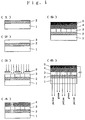
- FIG. 1 is a sectional view illustrating a manufacturing process according to one embodiment of this invention.
- Reference number 1 designates a glass substrate on which ITO (indium-tin oxide) 2 of sheet resistance 15 ⁇ / ⁇ is coated.
- ITO indium-tin oxide
- a polymer layer 3 rubberrene-dispersed PTPDMA layer
- a tris(8-quinolinolate)aluminum complex layer (hereafter referred to as Alq) 4 with green emission and expressed by the following formula: was formed on said polymer layer 3 as an electron transport layer 4 by depositing the material up to 400 ⁇ in a vacuum of 10 -5 Torr. Finally, in the same vacuum, Mg and Ag (10:1) were co-deposited up to 2000 ⁇ as a rear electrode 5, acting as a negative electrode. The light-emitting area was 0. 5 cm x 0. 5 cm.
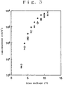
- 3 shows the luminescence-voltage characteristic obtained (in the figure, the triangular symbol indicates 1 wt.% of rubrene, the rectangular symbol indicates 3 wt.% of rubrene, the white circular symbol with a cross indicates 5 wt.% of rubrene, and the square symbol with a cross indicates 7 wt.% of rubrene).
- a yellow emission of up to 900 cd/m 2 was obtained at 12 V.
- the polymer layer 3 containing 3 wt.% of rubrene dispersed in polymer was formed on the ITO 2 on the glass substrate 1 up to 600 ⁇ in a similar manner, and the overall surface was irradiated with 240 mJ/cm 2 of i-line produced by a high-pressure mercury lamp in the air.
- the electron transport layer 4 was formed by depositing Alq on the polymer layer 3 up to 400 ⁇ under a vacuum of 10 -5 Torr. In the same vacuum, Mg and Ag (10:1) were co-deposited up to 2000 ⁇ as a rear electrode, which acted as a negative electrode 5.
- the light-emitting area was 0. 5 cm x 0. 5 cm.
- FIG. 2 (e) indicates that the luminescent color was green, and was thus emitted from Alq, and that rubrene did not emit light.
- FIG. 4 shows the luminescence-voltage characteristic obtained. As an initial characteristic, a green emission of up to 9000 cd/m 2 was obtained at about 10 V.
- the polymer layer 3 containing 3 wt.% of rubrene dispersed in polymer was formed on the ITO 2 on the glass substrate 1 up to 600 ⁇ in a similar manner [see FIG. 1(1) and (2)].
- a photo-mask 9 was placed on the polymer surface, and the element was partially irradiated with 240 mJ/cm 2 of i-line produced by a high-pressure mercury lamp in the air [see FIG. 1(3)].
- the electron transport layer 4 was formed by depositing Alq on polymer layer 3 up to 400 ⁇ in a vacuum of 10 -5 Torr [see FIG. 1(4)].
- Mg and Ag (10:1) were co-deposited up to 2000 ⁇ under the same vacuum with the rear electrode 5, acting as a negative electrode [see FIG. 1(5)].
- the light-emitting area was 0. 5 cm x 0. 5 cm.
- This organic EL element In this organic EL element, a direct current voltage was applied to produce emission from the light emitting layer, using ITO and Mg:Ag, respectively, as positive and negative electrodes. The unexposed portion emitted a green light, whereas the exposed area emitted a yellow light.
- This element is a multicolor display element having different luminescent colors on the same substrate (see the photographs included in the submitted documents).
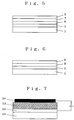
- FIG. 5 is a sectional view of Embodiment 2.
- Reference number 1 designates a glass substrate on which ITO (indium-tin oxide) 2 of sheet resistance 15 ⁇ / ⁇ is coated.
- a positive hole-transport layer 6 was formed on the ITO by depositing N,N'-bis (3-methylphenyl)-1,1'-biphenyl-4,4'-diamine (hereafter referred to as TPD) which has a positive hole transporting capability and has the following formula up to 400 ⁇ thickness in a vacuum of 10 -6 Torr.
- TPD N,N'-bis (3-methylphenyl)-1,1'-biphenyl-4,4'-diamine
- an Alq-rubrene layer 7 was formed as an electron transporting light emitting layer 7 by depositing Alq and rubrene thereon up to 600 ⁇ in a vacuum of 10 -5 Torr., so that the ratio of Alq to rubrene was 97 wt.% and 3 wt.%.
- Mg and Ag (10:1) were co-deposited up to 2000 ⁇ under the same vacuum, as a rear electrode 5, acting as a negative electrode.
- the light-emitting area was 0.5 cm x 0.5 cm.
- a layer 6 of thickness 400 ⁇ was formed on the ITO 2 on the glass substrate 1 in the same manner as described above, and an Alq-rubrene layer 7 was formed by co-depositing Alq and rubrene thereon up to 600 ⁇ in a vacuum of 10 -5 Torr., in the same ratio as described above.
- the overall surface was irradiated with 1200 mJ/cm 2 of i-line produced by a high-pressure mercury lamp in the air.
- Mg and Ag (10:1) were co-deposited on the Alq-rubrene layer 7 up to 2000 ⁇ under the same vacuum, as a rear electrode 5, acting as a negative electrode.
- the light-emitting area was 0. 5 cm x 0. 5 cm.
- TPD as a layer 6 of thickness 400 ⁇ was formed on the ITO 2 on the glass substrate 1 in the same manner, and an Alq-rubrene layer 7 was formed by co-depositing Alq and rubrene thereon up to 600 ⁇ in a vacuum of 10 -5 Torr., in the same ratio given above.
- a photo-mask 9 was placed on the polymer surface, and the element was partially irradiated with 1200 mJ/cm 2 of i-line produced by a high-pressure mercury lamp in the air.
- Mg and Ag (10:1) were co-deposited up to 2000 ⁇ under the vacuum as rear electrode 5, acting as a negative electrode.
- the light-emitting area was 0. 5 cm x 0. 5 cm.
- This organic EL element In this organic EL element, a direct current voltage was applied to produce emission from the light emitting layer, using ITO and Mg:Ag, respectively, as positive and negative electrodes. The exposed portion emitted a green light, indicating Alq, whereas the unexposed area emitted a yellow light, indicating rubrene.
- This element is a multicolor display element having different luminescent colors on the same substrate.
- FIG. 6 is a sectional view of Embodiment 3.
- Reference number 1 designates a glass substrate on which ITO (indium-tin oxide) 2 of sheet resistance 15 ⁇ / ⁇ is coated.
- PVK poly(N-vinylcarbazole)
- the PVK layer 8 containing 30 wt.% of PBD, 5 wt.% of TPB, and 3 wt.% of rubrene was formed on the ITO 2 on the glass substrate 1 as described above, and the overall surface was irradiated with 120 mJ/cm 2 of i-line produced by a high-pressure mercury lamp in the air.
- Mg and Ag (10:1) were co-deposited on the polymer layer 8 up to 2000 ⁇ in an identical vacuum, as a rear electrode 5, acting as a negative electrode.
- the light-emitting area was 0. 5 cm x 0. 5 cm.
- the PVK layer 8 containing 30 wt.% of PBD, 5 wt.% of TPB, and 3 wt.% of rubrene was formed on the ITO 2 on the glass substrate 1 in the same manner as described above.
- a photo-mask 9 was placed on the polymer surface, and the element was partially irradiated with 120 mJ/cm 2 of i-line produced by a high-pressure mercury lamp in the air.
- Mg and Ag (10:1) were co-deposited on the polymer layer 8 up to 2000 ⁇ under identical vacuum, as the rear electrode 5, acting as a negative electrode.
- the light-emitting area was 0. 5 cm x 0. 5 cm.
- This organic EL element In this organic EL element, a direct current voltage was applied to produce emission from the light emitting layer, using ITO and Mg:Ag, respectively, as positive and negative electrodes. The exposed portion emitted blue light, indicating TPB, whereas the unexposed area emitted yellow light, indicating rubrene.
- This element is a multicolor display element having different luminescent colors on the same substrate.
- FIG. 7 is a sectional view of an embodiment of this invention.
- Reference number 21 designates a glass substrate on which ITO (indium-tin oxide) 22 of sheet resistance 15 ⁇ / ⁇ is coated.
- Mg and Ag (10:1) were co-deposited up to 2000 ⁇ under the same
- a dye-dispersed PVK layer was formed on the ITO on the glass substrate up to 1000 ⁇ , and a high-pressure mercury lamp was then used to irradiate the layer with light corresponding to an absorption band of Nile Red, through a filter in the air, thereby subjecting only Nile Red to photo-oxidation to make it non-luminescent.
- Mg and Ag (10:1) were co-deposited on the polymer layer up to 2000 ⁇ under the same vacuum, as a rear electrode acting as a negative electrode.
- a direct current voltage was applied to produce emission from the light emitting layer, using ITO and Mg:Ag, respectively, as positive and negative electrodes. It was found that the luminescent color was green, thus emitted from coumarin 6, and that Nile Red did not emit light.
- a dye-dispersed PVK layer was formed on the ITO on the glass substrate up to 1000 ⁇ , and a high-pressure mercury lamp was then used to irradiate the layer with light corresponding to an absorption band of Nile Red, through a filter in the air. Then, the filter was changed to irradiate the layer with light corresponding to an absorption band of coumarin 6, thereby subjecting both Nile Red and coumarin 6 to photo-oxidation to render them non-luminescent.
- Mg and Ag (10:1) were then co-deposited on the polymer layer up to 2000 ⁇ under the identical vacuum, as a rear electrode, acting as a negative electrode.
- FIG. 8B 16 striped ITO electrodes (shown at 22) of width 3 mm were arranged on the glass substrate 21 in parallel at equal intervals (see FIGs. 8 and 9), and a dye-dispersed PVK layer 23 was formed up to 1000 ⁇ in a similar manner (FIG. 8B). Then, a photo-mask was placed on the polymer surface, and a high-pressure mercury lamp was used to irradiate two-thirds of the entire area of the PVK layer 23 with light through a filter in such a way that the layer was illuminated in stripes at an equal interval, thereby modifying only Nile Red (FIG. 8C).
- an active element such as a transistor may be added to each picture element of an RGB multicolor element to perform a memory function, thereby providing an active-matrix RGB dot-matrix display, or a full-color display.
Applications Claiming Priority (4)
| Application Number | Priority Date | Filing Date | Title |
|---|---|---|---|
| JP14494896 | 1996-05-15 | ||
| JP144948/96 | 1996-05-15 | ||
| JP14494896 | 1996-05-15 | ||
| PCT/JP1997/001626 WO1997043874A1 (fr) | 1996-05-15 | 1997-05-14 | Element organique multicolore 'el', procede de fabrication associe et affichage mettant en oeuvre cet element |
Publications (3)
| Publication Number | Publication Date |
|---|---|
| EP0903965A1 true EP0903965A1 (fr) | 1999-03-24 |
| EP0903965A4 EP0903965A4 (fr) | 1999-07-28 |
| EP0903965B1 EP0903965B1 (fr) | 2003-07-30 |
Family
ID=15373918
Family Applications (1)
| Application Number | Title | Priority Date | Filing Date |
|---|---|---|---|
| EP97922051A Expired - Lifetime EP0903965B1 (fr) | 1996-05-15 | 1997-05-14 | Element organique multicolore "el", procede de fabrication associe et affichage mettant en oeuvre cet element |
Country Status (13)
| Country | Link |
|---|---|
| US (2) | US6459199B1 (fr) |
| EP (1) | EP0903965B1 (fr) |
| JP (1) | JP3849066B2 (fr) |
| CN (1) | CN1123278C (fr) |
| AT (1) | ATE246437T1 (fr) |
| AU (1) | AU713944B2 (fr) |
| BR (1) | BR9709312A (fr) |
| CA (1) | CA2253819C (fr) |
| DE (1) | DE69723831T2 (fr) |
| NZ (1) | NZ332736A (fr) |
| RU (1) | RU2173508C2 (fr) |
| TW (1) | TW542851B (fr) |
| WO (1) | WO1997043874A1 (fr) |
Cited By (12)
| Publication number | Priority date | Publication date | Assignee | Title |
|---|---|---|---|---|
| WO2002011209A2 (fr) * | 2000-08-01 | 2002-02-07 | Emagin Corporation | Procede de configuration de supports de changement de couleur pour dispositifs d'affichage a diode electroluminescente organique |
| WO2002058935A2 (fr) * | 2000-12-28 | 2002-08-01 | Polaroid Corporation | Tete d'impression d'un seul tenant a fibres optiques et a diodes electroluminescentes organiques, dotee de filtres colores |
| EP1289015A2 (fr) | 2001-08-28 | 2003-03-05 | Konica Corporation | Dispositif émetteur de lumière en plusieurs couleurs et procédé de production de ce dispositif |
| WO2003086025A1 (fr) * | 2002-03-29 | 2003-10-16 | The Government Of The United States As Represented By The Secretary Of The Navy | Structuration rvb de diodes organiques electroluminescentes, au moyen de materiaux emissifs decolorables par rayonnement lumineux disperses dans un hote commun |
| WO2003100879A2 (fr) * | 2002-05-29 | 2003-12-04 | Austria Wirtschaftsservice Gesellschaft M.B.H. | Composant luminescent |
| WO2004084315A1 (fr) * | 2003-03-21 | 2004-09-30 | Fraunhofer-Gesellschaft zur Förderung der angewandten Forschung e.V. | Procede pour modifier une propriete de conversion d'une couche de conversion de spectre pour un composant electroluminescent |
| WO2004075604A3 (fr) * | 2003-02-19 | 2004-11-11 | Lg Electronics Inc | Dispositif electroluminescent organique et son procede de fabrication |
| WO2010010523A3 (fr) * | 2008-07-24 | 2010-04-01 | Koninklijke Philips Electronics N.V. | Dispositif et procédé d'éclairage |
| US8358057B2 (en) | 2007-03-29 | 2013-01-22 | Japan Display Central Inc. | Organic EL display and method of manufacturing the same |
| KR101308282B1 (ko) * | 2005-09-05 | 2013-09-13 | 이데미쓰 고산 가부시키가이샤 | 청색 발광 유기 전계 발광 소자 |
| US9028975B2 (en) | 2006-05-04 | 2015-05-12 | Lg Chem, Ltd. | Organic light-emitting device having light-emitting pattern, method and apparatus for preparing the same |
| US9397308B2 (en) | 2006-12-04 | 2016-07-19 | Semiconductor Energy Laboratory Co., Ltd. | Light emitting element, light emitting device, and electronic device |
Families Citing this family (62)
| Publication number | Priority date | Publication date | Assignee | Title |
|---|---|---|---|---|
| JP2001185350A (ja) * | 1999-12-24 | 2001-07-06 | Sanyo Electric Co Ltd | 被着用マスク、その製造方法、エレクトロルミネッセンス表示装置及びその製造方法 |
| JP4890669B2 (ja) * | 2000-03-13 | 2012-03-07 | Tdk株式会社 | 有機el素子 |
| US7153592B2 (en) * | 2000-08-31 | 2006-12-26 | Fujitsu Limited | Organic EL element and method of manufacturing the same, organic EL display device using the element, organic EL material, and surface emission device and liquid crystal display device using the material |
| JP2002304136A (ja) * | 2001-01-17 | 2002-10-18 | Seiko Epson Corp | 有機エレクトロルミネッセンス表示装置を備えた電子機器 |
| JP4632191B2 (ja) * | 2001-04-20 | 2011-02-16 | 大日本印刷株式会社 | 光触媒含有層を有するel素子とその製造方法 |
| JP2003017264A (ja) * | 2001-04-27 | 2003-01-17 | Canon Inc | 電界発光素子及び画像表示装置 |
| JP4617031B2 (ja) * | 2001-08-24 | 2011-01-19 | 大日本印刷株式会社 | 光分解性染料を用いたel素子 |
| US6716656B2 (en) * | 2001-09-04 | 2004-04-06 | The Trustees Of Princeton University | Self-aligned hybrid deposition |
| KR100437533B1 (ko) * | 2002-05-29 | 2004-06-30 | 엘지.필립스 엘시디 주식회사 | 액티브 매트릭스형 유기전계발광 소자 및 그의 제조방법 |
| JP3974023B2 (ja) * | 2002-06-27 | 2007-09-12 | 富士通株式会社 | 半導体装置の製造方法 |
| US6720092B2 (en) * | 2002-07-08 | 2004-04-13 | Eastman Kodak Company | White organic light-emitting devices using rubrene layer |
| KR20050017169A (ko) * | 2003-08-08 | 2005-02-22 | 삼성에스디아이 주식회사 | 애노드 표면 개질층을 사용하는 유기 전계 발광 소자 |
| KR101246247B1 (ko) * | 2003-08-29 | 2013-03-21 | 가부시키가이샤 한도오따이 에네루기 켄큐쇼 | 전계발광소자 및 그것을 구비한 발광장치 |
| US20060139342A1 (en) * | 2004-12-29 | 2006-06-29 | Gang Yu | Electronic devices and processes for forming electronic devices |
| US20050136289A1 (en) * | 2003-12-22 | 2005-06-23 | Chu Hye Y. | White organic light emitting device |
| JP4985343B2 (ja) * | 2004-03-11 | 2012-07-25 | 三菱化学株式会社 | 電荷輸送膜用組成物、及び、それを用いた有機電界発光素子 |
| KR100963457B1 (ko) * | 2004-03-11 | 2010-06-17 | 미쓰비시 가가꾸 가부시키가이샤 | 전하 수송막용 조성물 및 이온 화합물, 이를 이용한 전하수송막 및 유기 전계 발광 장치, 및 유기 전계 발광 장치의제조 방법 및 전하 수송막의 제조 방법 |
| JP4724875B2 (ja) * | 2004-04-30 | 2011-07-13 | 独立行政法人産業技術総合研究所 | 有機電界発光素子の製造方法 |
| JP2006012786A (ja) * | 2004-06-22 | 2006-01-12 | Samsung Sdi Co Ltd | 有機電界発光素子、並びに該製造方法 |
| DE102004031071B4 (de) * | 2004-06-22 | 2008-04-30 | Samsung SDI Co., Ltd., Suwon | Verfahren zur Behandlung einer organischen Leuchtdiode (OLED) zur Verlängerung der Lebensdauer |
| JP4925569B2 (ja) * | 2004-07-08 | 2012-04-25 | ローム株式会社 | 有機エレクトロルミネッセント素子 |
| US7504163B2 (en) * | 2004-07-12 | 2009-03-17 | Eastman Kodak Company | Hole-trapping materials for improved OLED efficiency |
| CA2574841A1 (fr) * | 2004-07-27 | 2006-02-09 | University Of Washington | Dispositif electroluminescent emettant de la lumiere blanche |
| KR100669718B1 (ko) * | 2004-07-29 | 2007-01-16 | 삼성에스디아이 주식회사 | 유기 전계 발광 소자 |
| DE102004042356A1 (de) * | 2004-09-01 | 2006-03-02 | Siemens Ag | Anzeigeeinheit und Verfahren zur Herstellung einer Anzeigeeinheit |
| KR100637177B1 (ko) * | 2004-10-11 | 2006-10-23 | 삼성에스디아이 주식회사 | 유기 전계 발광 소자 |
| US20060141135A1 (en) * | 2004-12-29 | 2006-06-29 | Jian Wang | Processes for forming layers for electronic devices using heating elements |
| US7268006B2 (en) | 2004-12-30 | 2007-09-11 | E.I. Du Pont De Nemours And Company | Electronic device including a guest material within a layer and a process for forming the same |
| US8691667B1 (en) | 2004-12-30 | 2014-04-08 | E. I. Du Pont De Nemours And Company | Method and apparatus for depositing a pattern on a substrate |
| US7584701B2 (en) * | 2004-12-30 | 2009-09-08 | E.I. Du Pont De Nemours And Company | Processes for printing layers for electronic devices and printing apparatuses for performing the processes |
| US20060146079A1 (en) * | 2004-12-30 | 2006-07-06 | Macpherson Charles D | Process and apparatus for forming an electronic device |
| US20060228466A1 (en) * | 2004-12-30 | 2006-10-12 | Gang Yu | Solution dispense and patterning process and apparatus |
| US7469638B2 (en) * | 2004-12-30 | 2008-12-30 | E.I. Du Pont De Nemours And Company | Electronic devices and processes for forming the same |
| US20060145598A1 (en) * | 2004-12-30 | 2006-07-06 | Macpherson Charles D | Electronic devices and process for forming the same |
| US20070152209A1 (en) * | 2005-12-19 | 2007-07-05 | Uckert Frank P | Devices using polymers based on 3,6- and 2,7-conjugated poly(phenanthrene) |
| US7795653B2 (en) * | 2005-12-27 | 2010-09-14 | E. I. Du Pont De Nemours And Company | Electronic device including space-apart radiation regions and a process for forming the same |
| US7960717B2 (en) * | 2005-12-29 | 2011-06-14 | E.I. Du Pont De Nemours And Company | Electronic device and process for forming same |
| CN101438626B (zh) * | 2006-05-04 | 2012-11-07 | Lg化学株式会社 | 具有发光图案的有机发光器件、制备该器件的方法和设备 |
| TWI378740B (en) * | 2006-10-04 | 2012-12-01 | Ritdisplay Corp | Full-color organic light emitting diode display panel and method thereof |
| GB0625540D0 (en) * | 2006-12-22 | 2007-01-31 | Oled T Ltd | Electroluminescent devices |
| TW200912848A (en) * | 2007-04-26 | 2009-03-16 | Sony Corp | Display correction circuit of organic EL panel |
| JP2009111023A (ja) * | 2007-10-26 | 2009-05-21 | Toshiba Matsushita Display Technology Co Ltd | 有機el表示装置及びその製造方法 |
| JP4745362B2 (ja) * | 2008-03-31 | 2011-08-10 | 東芝モバイルディスプレイ株式会社 | 有機el装置及びその製造方法 |
| TWI470787B (zh) | 2008-03-31 | 2015-01-21 | Japan Display Inc | 有機el顯示裝置及其製造方法 |
| JP4544645B2 (ja) * | 2008-04-25 | 2010-09-15 | 東芝モバイルディスプレイ株式会社 | 有機el表示装置の製造方法 |
| KR20110011695A (ko) * | 2008-05-19 | 2011-02-08 | 이 아이 듀폰 디 네모아 앤드 캄파니 | 박층을 용액 코팅하는 장치 및 방법 |
| JP2010056526A (ja) * | 2008-07-31 | 2010-03-11 | Canon Inc | 有機エレクトロルミネセンス素子および画像表示装置および撮像装置 |
| JP4775863B2 (ja) | 2008-09-26 | 2011-09-21 | 東芝モバイルディスプレイ株式会社 | 有機el表示装置及びその製造方法 |
| JP5448030B2 (ja) * | 2008-11-19 | 2014-03-19 | 新日鐵住金株式会社 | 超音波探傷方法及び装置 |
| JP5580335B2 (ja) * | 2008-12-27 | 2014-08-27 | イー・アイ・デュポン・ドウ・ヌムール・アンド・カンパニー | 連続印刷用の飛散防止装置および方法 |
| JP4775865B2 (ja) * | 2009-01-14 | 2011-09-21 | 東芝モバイルディスプレイ株式会社 | 有機el表示装置及びその製造方法 |
| JP5305267B2 (ja) * | 2009-08-04 | 2013-10-02 | 株式会社ジャパンディスプレイ | 有機el装置 |
| US20110193066A1 (en) * | 2009-08-13 | 2011-08-11 | E. I. Du Pont De Nemours And Company | Current limiting element for pixels in electronic devices |
| JP4942223B2 (ja) * | 2009-11-25 | 2012-05-30 | 東芝モバイルディスプレイ株式会社 | 有機el装置 |
| US20110108812A1 (en) * | 2009-11-06 | 2011-05-12 | Shiro Sumita | Organic el device |
| JP2011191739A (ja) | 2010-02-16 | 2011-09-29 | Toshiba Mobile Display Co Ltd | 有機エレクトロルミネッセンス装置 |
| TWI567075B (zh) * | 2010-06-15 | 2017-01-21 | 國立清華大學 | 6H-吲哚〔3,2-b〕喹喔啉衍生物及其有機發光二極體 |
| CN102329334B (zh) * | 2010-07-13 | 2016-03-16 | 郑建鸿 | 6H-吲哚[3,2-b]喹喔啉衍生物及其有机发光二极管 |
| JP4997513B2 (ja) * | 2010-12-14 | 2012-08-08 | 独立行政法人産業技術総合研究所 | 有機電界発光素子の製造方法 |
| JP5837316B2 (ja) * | 2011-03-25 | 2015-12-24 | 株式会社Joled | 有機el表示装置およびその製造方法 |
| JP6207263B2 (ja) * | 2013-07-03 | 2017-10-04 | 株式会社ジャパンディスプレイ | 有機el表示装置、及びその製造方法 |
| WO2018181049A1 (fr) * | 2017-03-30 | 2018-10-04 | 株式会社クオルテック | Procédé de fabrication de panneau d'affichage el, dispositif de fabrication pour panneau d'affichage el, panneau d'affichage el et dispositif d'affichage el |
Family Cites Families (66)
| Publication number | Priority date | Publication date | Assignee | Title |
|---|---|---|---|---|
| JPS58196582A (ja) * | 1982-05-12 | 1983-11-16 | セイコーインスツルメンツ株式会社 | 表示素子 |
| US4539507A (en) | 1983-03-25 | 1985-09-03 | Eastman Kodak Company | Organic electroluminescent devices having improved power conversion efficiencies |
| JPS6075864A (ja) * | 1983-09-30 | 1985-04-30 | 関西日本電気株式会社 | El表示装置の製造方法 |
| US4720432A (en) | 1987-02-11 | 1988-01-19 | Eastman Kodak Company | Electroluminescent device with organic luminescent medium |
| JPH0288689A (ja) | 1988-09-26 | 1990-03-28 | Mitsubishi Kasei Corp | 電界発光素子 |
| EP0373582B1 (fr) | 1988-12-14 | 1995-03-01 | Idemitsu Kosan Company Limited | Dispositif électro-luminescent |
| JPH02289676A (ja) | 1989-01-13 | 1990-11-29 | Ricoh Co Ltd | 電界発光素子 |
| JP2651233B2 (ja) | 1989-01-20 | 1997-09-10 | 出光興産株式会社 | 薄膜有機el素子 |
| JPH02196885A (ja) | 1989-01-25 | 1990-08-03 | Asahi Chem Ind Co Ltd | 有機電界発光素子 |
| US5130603A (en) | 1989-03-20 | 1992-07-14 | Idemitsu Kosan Co., Ltd. | Organic electroluminescence device |
| JP2879080B2 (ja) | 1989-03-23 | 1999-04-05 | 株式会社リコー | 電界発光素子 |
| JPH07119408B2 (ja) | 1989-03-28 | 1995-12-20 | 出光興産株式会社 | 有機エレクトロルミネッセンス素子 |
| JPH02255789A (ja) | 1989-03-29 | 1990-10-16 | Asahi Chem Ind Co Ltd | 有機電場発光素子 |
| JPH0820642B2 (ja) * | 1989-08-21 | 1996-03-04 | シャープ株式会社 | 液晶表示装置 |
| JP2554771B2 (ja) | 1989-12-28 | 1996-11-13 | 出光興産株式会社 | 芳香族ジメチリディン化合物 |
| JPH03296595A (ja) | 1990-04-13 | 1991-12-27 | Kao Corp | 有機薄膜エレクトロルミネッセンス素子 |
| JPH0474895A (ja) | 1990-07-16 | 1992-03-10 | Nisshin Steel Co Ltd | アルミニウム電気めっき装置 |
| JP2997021B2 (ja) | 1990-08-10 | 2000-01-11 | パイオニア株式会社 | 有機エレクトロルミネッセンス素子 |
| JPH0474895U (fr) * | 1990-11-09 | 1992-06-30 | ||
| JP2891784B2 (ja) | 1991-02-06 | 1999-05-17 | パイオニア株式会社 | 有機エレクトロルミネッセンス素子 |
| JP2891783B2 (ja) | 1991-02-06 | 1999-05-17 | パイオニア株式会社 | 有機エレクトロルミネッセンス素子 |
| JP2793373B2 (ja) * | 1991-02-07 | 1998-09-03 | 出光興産株式会社 | 有機エレクトロルミネッセンス素子のパターン化方法 |
| US5294870A (en) * | 1991-12-30 | 1994-03-15 | Eastman Kodak Company | Organic electroluminescent multicolor image display device |
| JPH05202011A (ja) | 1992-01-27 | 1993-08-10 | Toshiba Corp | オキサジアゾール誘導体 |
| JPH0649079A (ja) | 1992-04-02 | 1994-02-22 | Idemitsu Kosan Co Ltd | シラナミン誘導体およびその製造方法並びに該シラナミン誘導体を用いたel素子 |
| JPH06107648A (ja) | 1992-09-29 | 1994-04-19 | Ricoh Co Ltd | 新規なオキサジアゾール化合物 |
| JPH0625659A (ja) | 1992-07-07 | 1994-02-01 | Idemitsu Kosan Co Ltd | ホスファミン誘導体、その製造方法およびそれを用いたエレクトロルミネッセンス素子 |
| JP3341090B2 (ja) | 1992-07-27 | 2002-11-05 | 株式会社リコー | オキサジアゾール誘導体ならびにその製造法 |
| JP3228301B2 (ja) | 1992-09-07 | 2001-11-12 | 出光興産株式会社 | 有機エレクトロルミネッセンス素子 |
| JP3163589B2 (ja) | 1992-09-21 | 2001-05-08 | 出光興産株式会社 | 有機エレクトロルミネッセンス素子 |
| JPH06206865A (ja) | 1992-10-14 | 1994-07-26 | Chisso Corp | 新規アントラセン化合物と該化合物を用いる電界発光素子 |
| JP3287421B2 (ja) | 1992-10-19 | 2002-06-04 | 出光興産株式会社 | 有機エレクトロルミネッセンス素子 |
| JPH06145146A (ja) | 1992-11-06 | 1994-05-24 | Chisso Corp | オキシネイト誘導体 |
| JP3366401B2 (ja) | 1992-11-20 | 2003-01-14 | 出光興産株式会社 | 白色有機エレクトロルミネッセンス素子 |
| JPH06203963A (ja) | 1993-01-08 | 1994-07-22 | Idemitsu Kosan Co Ltd | 有機エレクトロルミネッセンス素子 |
| JPH06215874A (ja) | 1993-01-20 | 1994-08-05 | Idemitsu Kosan Co Ltd | 有機エレクトロルミネッセンス素子 |
| JP3419534B2 (ja) | 1993-02-10 | 2003-06-23 | 靖彦 城田 | トリスアリールアミノベンゼン誘導体、有機el素子用化合物および有機el素子 |
| JP3214674B2 (ja) | 1993-03-26 | 2001-10-02 | 出光興産株式会社 | 新規スチリル化合物,その製造法およびそれからなる有機エレクトロルミネッセンス素子 |
| JP3211994B2 (ja) | 1993-03-26 | 2001-09-25 | 出光興産株式会社 | 4官能スチリル化合物およびその製造法 |
| JPH06293778A (ja) | 1993-04-05 | 1994-10-21 | Idemitsu Kosan Co Ltd | シラナミン誘導体およびその製造方法 |
| JP3549555B2 (ja) | 1993-10-04 | 2004-08-04 | 株式会社リコー | 新規なピレン誘導体ならびにその製造方法 |
| JP3220950B2 (ja) | 1993-11-01 | 2001-10-22 | 保土谷化学工業株式会社 | ベンジジン化合物 |
| JP3574860B2 (ja) | 1993-11-01 | 2004-10-06 | 保土谷化学工業株式会社 | テトラフェニルベンジジン化合物 |
| JPH07145116A (ja) | 1993-11-25 | 1995-06-06 | Nisshinbo Ind Inc | 芳香族ジアミン化合物 |
| JPH07157473A (ja) | 1993-12-06 | 1995-06-20 | Chisso Corp | トリアジン誘導体、その製造法及びそれを用いた電界発光素子 |
| JP3300827B2 (ja) | 1993-12-21 | 2002-07-08 | 株式会社リコー | オキサジアゾール化合物およびその製造法 |
| JP3539995B2 (ja) | 1993-12-21 | 2004-07-07 | 株式会社リコー | オキサジアゾール化合物およびその製造法 |
| JP3594642B2 (ja) | 1993-12-24 | 2004-12-02 | 保土谷化学工業株式会社 | ジアミノジフェニル化合物及び該化合物を用いた有機電界発光素子 |
| JP3496080B2 (ja) | 1993-12-24 | 2004-02-09 | 株式会社リコー | オキサジアゾール誘導体およびその製造方法 |
| JP3579746B2 (ja) | 1994-02-07 | 2004-10-20 | チッソ株式会社 | ジフェニルアミン誘導体 |
| JP3828595B2 (ja) | 1994-02-08 | 2006-10-04 | Tdk株式会社 | 有機el素子 |
| US5409783A (en) * | 1994-02-24 | 1995-04-25 | Eastman Kodak Company | Red-emitting organic electroluminescent device |
| US6064355A (en) | 1994-05-24 | 2000-05-16 | Texas Instruments Incorporated | Method and apparatus for playback with a virtual reality system |
| JPH081472A (ja) | 1994-06-17 | 1996-01-09 | Toshiba Mach Co Ltd | 移動体移動装置 |
| JP3593719B2 (ja) | 1994-08-04 | 2004-11-24 | 東洋インキ製造株式会社 | 新規なトリフェニルアミン誘導体、その製造方法及び用途 |
| JP3593717B2 (ja) | 1994-08-04 | 2004-11-24 | 東洋インキ製造株式会社 | 新規なトリフェニルアミン誘導体、その製造方法及び用途 |
| JP3593718B2 (ja) | 1994-08-04 | 2004-11-24 | 東洋インキ製造株式会社 | 新規なトリフェニルアミン誘導体、その製造方法及び用途 |
| JP3786438B2 (ja) * | 1994-08-29 | 2006-06-14 | アヴェンティス・リサーチ・ウント・テクノロジーズ・ゲーエムベーハー・ウント・コー・カーゲー | 光照射によるポリアリレンビニレンポリマー薄膜のパターン化 |
| JP2800935B2 (ja) * | 1995-03-24 | 1998-09-21 | 東亞合成株式会社 | 発光表示素子及びその製造方法 |
| JP3234131B2 (ja) * | 1995-06-23 | 2001-12-04 | 株式会社東芝 | 液晶表示装置 |
| EP0784659B1 (fr) * | 1995-08-03 | 1999-12-08 | Koninklijke Philips Electronics N.V. | Dispositif electroluminescent |
| US5736754A (en) * | 1995-11-17 | 1998-04-07 | Motorola, Inc. | Full color organic light emitting diode array |
| KR0170490B1 (ko) * | 1995-12-22 | 1999-05-01 | 양승택 | 전기장 발광 고분자를 이용한 칼라 디스플레이 소자 및 그 제조방법 |
| US5683823A (en) * | 1996-01-26 | 1997-11-04 | Eastman Kodak Company | White light-emitting organic electroluminescent devices |
| JP3599077B2 (ja) * | 1996-05-15 | 2004-12-08 | ケミプロ化成株式会社 | 有機エレクトロルミネッセンス素子とその製造方法 |
| US6037190A (en) * | 1998-11-13 | 2000-03-14 | Industrial Technology Research Institute | Method for fabricating an organic electro-luminescent device |
-
1997
- 1997-05-14 CN CN97194632A patent/CN1123278C/zh not_active Expired - Fee Related
- 1997-05-14 EP EP97922051A patent/EP0903965B1/fr not_active Expired - Lifetime
- 1997-05-14 US US09/171,966 patent/US6459199B1/en not_active Expired - Lifetime
- 1997-05-14 RU RU98122365/28A patent/RU2173508C2/ru not_active IP Right Cessation
- 1997-05-14 AT AT97922051T patent/ATE246437T1/de not_active IP Right Cessation
- 1997-05-14 JP JP54074197A patent/JP3849066B2/ja not_active Expired - Fee Related
- 1997-05-14 BR BR9709312A patent/BR9709312A/pt not_active Application Discontinuation
- 1997-05-14 TW TW086106403A patent/TW542851B/zh not_active IP Right Cessation
- 1997-05-14 DE DE69723831T patent/DE69723831T2/de not_active Expired - Lifetime
- 1997-05-14 WO PCT/JP1997/001626 patent/WO1997043874A1/fr active IP Right Grant
- 1997-05-14 AU AU27888/97A patent/AU713944B2/en not_active Ceased
- 1997-05-14 NZ NZ332736A patent/NZ332736A/en unknown
- 1997-05-14 CA CA002253819A patent/CA2253819C/fr not_active Expired - Fee Related
-
2002
- 2002-08-19 US US10/222,929 patent/US20030057827A1/en not_active Abandoned
Non-Patent Citations (2)
| Title |
|---|
| No further relevant documents disclosed * |
| See also references of WO9743874A1 * |
Cited By (21)
| Publication number | Priority date | Publication date | Assignee | Title |
|---|---|---|---|---|
| WO2002011209A2 (fr) * | 2000-08-01 | 2002-02-07 | Emagin Corporation | Procede de configuration de supports de changement de couleur pour dispositifs d'affichage a diode electroluminescente organique |
| WO2002011209A3 (fr) * | 2000-08-01 | 2002-05-02 | Emagin Corp | Procede de configuration de supports de changement de couleur pour dispositifs d'affichage a diode electroluminescente organique |
| WO2002058935A2 (fr) * | 2000-12-28 | 2002-08-01 | Polaroid Corporation | Tete d'impression d'un seul tenant a fibres optiques et a diodes electroluminescentes organiques, dotee de filtres colores |
| WO2002058935A3 (fr) * | 2000-12-28 | 2003-07-24 | Polaroid Corp | Tete d'impression d'un seul tenant a fibres optiques et a diodes electroluminescentes organiques, dotee de filtres colores |
| EP1289015A2 (fr) | 2001-08-28 | 2003-03-05 | Konica Corporation | Dispositif émetteur de lumière en plusieurs couleurs et procédé de production de ce dispositif |
| KR100886976B1 (ko) * | 2001-08-28 | 2009-03-04 | 코니카 미놀타 홀딩스 가부시키가이샤 | 다색 발광 장치 및 그의 제조 방법 |
| EP1289015A3 (fr) * | 2001-08-28 | 2007-04-25 | Konica Corporation | Dispositif émetteur de lumière en plusieurs couleurs et procédé de production de ce dispositif |
| WO2003086025A1 (fr) * | 2002-03-29 | 2003-10-16 | The Government Of The United States As Represented By The Secretary Of The Navy | Structuration rvb de diodes organiques electroluminescentes, au moyen de materiaux emissifs decolorables par rayonnement lumineux disperses dans un hote commun |
| AT413925B (de) * | 2002-05-29 | 2006-07-15 | Wolfgang Dr Kern | Lichtemittierendes bauelement |
| WO2003100879A3 (fr) * | 2002-05-29 | 2004-05-13 | Wolfgang Kern | Composant luminescent |
| WO2003100879A2 (fr) * | 2002-05-29 | 2003-12-04 | Austria Wirtschaftsservice Gesellschaft M.B.H. | Composant luminescent |
| WO2004075604A3 (fr) * | 2003-02-19 | 2004-11-11 | Lg Electronics Inc | Dispositif electroluminescent organique et son procede de fabrication |
| US7541097B2 (en) | 2003-02-19 | 2009-06-02 | Lg Display Co., Ltd. | Organic electroluminescent device and method for fabricating the same |
| WO2004084315A1 (fr) * | 2003-03-21 | 2004-09-30 | Fraunhofer-Gesellschaft zur Förderung der angewandten Forschung e.V. | Procede pour modifier une propriete de conversion d'une couche de conversion de spectre pour un composant electroluminescent |
| DE10312679B4 (de) * | 2003-03-21 | 2006-08-31 | Fraunhofer-Gesellschaft zur Förderung der angewandten Forschung e.V. | Verfahren zum Ändern einer Umwandlungseigenschaft einer Spektrumsumwandlungsschicht für ein lichtemittierendes Bauelement |
| KR101308282B1 (ko) * | 2005-09-05 | 2013-09-13 | 이데미쓰 고산 가부시키가이샤 | 청색 발광 유기 전계 발광 소자 |
| US9028975B2 (en) | 2006-05-04 | 2015-05-12 | Lg Chem, Ltd. | Organic light-emitting device having light-emitting pattern, method and apparatus for preparing the same |
| US9397308B2 (en) | 2006-12-04 | 2016-07-19 | Semiconductor Energy Laboratory Co., Ltd. | Light emitting element, light emitting device, and electronic device |
| US8358057B2 (en) | 2007-03-29 | 2013-01-22 | Japan Display Central Inc. | Organic EL display and method of manufacturing the same |
| WO2010010523A3 (fr) * | 2008-07-24 | 2010-04-01 | Koninklijke Philips Electronics N.V. | Dispositif et procédé d'éclairage |
| US9276229B2 (en) | 2008-07-24 | 2016-03-01 | Koninklijke Philips N.V. | Device and method for lighting |
Also Published As
| Publication number | Publication date |
|---|---|
| EP0903965A4 (fr) | 1999-07-28 |
| CA2253819C (fr) | 2004-11-02 |
| EP0903965B1 (fr) | 2003-07-30 |
| CN1218604A (zh) | 1999-06-02 |
| RU2173508C2 (ru) | 2001-09-10 |
| DE69723831D1 (de) | 2003-09-04 |
| DE69723831T2 (de) | 2004-05-27 |
| AU2788897A (en) | 1997-12-05 |
| BR9709312A (pt) | 1999-08-10 |
| CA2253819A1 (fr) | 1997-11-20 |
| NZ332736A (en) | 1999-09-29 |
| WO1997043874A1 (fr) | 1997-11-20 |
| ATE246437T1 (de) | 2003-08-15 |
| US20030057827A1 (en) | 2003-03-27 |
| TW542851B (en) | 2003-07-21 |
| CN1123278C (zh) | 2003-10-01 |
| US6459199B1 (en) | 2002-10-01 |
| JP3849066B2 (ja) | 2006-11-22 |
| AU713944B2 (en) | 1999-12-16 |
Similar Documents
| Publication | Publication Date | Title |
|---|---|---|
| EP0903965B1 (fr) | Element organique multicolore "el", procede de fabrication associe et affichage mettant en oeuvre cet element | |
| EP0847228B1 (fr) | Substance pour dispositif organique électroluminescent et son utilisation | |
| EP1089361B1 (fr) | Dispositif électroluminescent organique et méthode de contrôle du spectre d'émission | |
| EP0866110B1 (fr) | Substance émettant de la lumière pour dispositif organique électroluminescent et dispositif organique électroluminescent | |
| KR100903918B1 (ko) | 유기 전계발광 소자 및 표시 장치 | |
| EP1469533A2 (fr) | Dispositif électroluminescent organique supprimant la génération de la lumière ultraviolette et système d'éclairage utilisant un élément électroluminescent organique | |
| JP4824848B2 (ja) | 有機エレクトロルミネッセント素子、有機エレクトロルミネッセント素子群及びその発光スペクトルの特定方法 | |
| KR100886976B1 (ko) | 다색 발광 장치 및 그의 제조 방법 | |
| JP4048521B2 (ja) | 発光素子 | |
| EP1480280A2 (fr) | Dispositif organique électroluminescent et sa méthode de fabrication | |
| JP2001102175A (ja) | 有機エレクトロルミネッセント素子、有機エレクトロルミネッセント素子群及びその発光スペクトルの制御方法 | |
| JPH11162643A (ja) | 有機エレクトロルミネセント装置 | |
| KR100471523B1 (ko) | 멀티칼라유기이엘소자,그제법및그것을사용한디스플레이 | |
| JP3599077B2 (ja) | 有機エレクトロルミネッセンス素子とその製造方法 | |
| JP2001131434A (ja) | 光変性可能な発光性有機色素およびそれを用いたマルチカラー有機el素子 | |
| JP2000150152A (ja) | 有機エレクトロルミネッセンス表示装置 | |
| JP2003109768A (ja) | 発光素子 | |
| JP3151997B2 (ja) | 有機エレクトロルミネッセンス素子 | |
| JP2000150161A (ja) | 有機エレクトロルミネッセンス表示装置 | |
| JP3246053B2 (ja) | 有機エレクトロルミネッセンス素子 | |
| JPH10270167A (ja) | 新規発光材料、新規電子輸送材料およびそれを用いた有機el素子 | |
| MXPA98009461A (en) | Elemento the organic, multicolor, method to manufacture it and element of presentation that uses the mi | |
| JP3456873B2 (ja) | 有機エレクトロルミネッセンス素子 | |
| JP2001319788A (ja) | 電界発光素子 | |
| JP2009100002A (ja) | 有機エレクトロルミネッセンス素子及び表示装置 |
Legal Events
| Date | Code | Title | Description |
|---|---|---|---|
| PUAI | Public reference made under article 153(3) epc to a published international application that has entered the european phase |
Free format text: ORIGINAL CODE: 0009012 |
|
| 17P | Request for examination filed |
Effective date: 19981112 |
|
| AK | Designated contracting states |
Kind code of ref document: A1 Designated state(s): AT BE DE ES FR GB IT NL PT |
|
| A4 | Supplementary search report drawn up and despatched |
Effective date: 19990616 |
|
| AK | Designated contracting states |
Kind code of ref document: A4 Designated state(s): AT BE DE ES FR GB IT NL PT |
|
| RIC1 | Information provided on ipc code assigned before grant |
Free format text: 6H 05B 33/18 A, 6H 05B 33/10 B, 6H 05B 33/14 B |
|
| GRAH | Despatch of communication of intention to grant a patent |
Free format text: ORIGINAL CODE: EPIDOS IGRA |
|
| GRAH | Despatch of communication of intention to grant a patent |
Free format text: ORIGINAL CODE: EPIDOS IGRA |
|
| GRAA | (expected) grant |
Free format text: ORIGINAL CODE: 0009210 |
|
| AK | Designated contracting states |
Designated state(s): AT BE DE ES FR GB IT NL PT |
|
| PG25 | Lapsed in a contracting state [announced via postgrant information from national office to epo] |
Ref country code: IT Free format text: LAPSE BECAUSE OF FAILURE TO SUBMIT A TRANSLATION OF THE DESCRIPTION OR TO PAY THE FEE WITHIN THE PRESCRIBED TIME-LIMIT;WARNING: LAPSES OF ITALIAN PATENTS WITH EFFECTIVE DATE BEFORE 2007 MAY HAVE OCCURRED AT ANY TIME BEFORE 2007. THE CORRECT EFFECTIVE DATE MAY BE DIFFERENT FROM THE ONE RECORDED. Effective date: 20030730 Ref country code: FR Free format text: LAPSE BECAUSE OF NON-PAYMENT OF DUE FEES Effective date: 20030730 Ref country code: BE Free format text: LAPSE BECAUSE OF FAILURE TO SUBMIT A TRANSLATION OF THE DESCRIPTION OR TO PAY THE FEE WITHIN THE PRESCRIBED TIME-LIMIT Effective date: 20030730 Ref country code: AT Free format text: LAPSE BECAUSE OF FAILURE TO SUBMIT A TRANSLATION OF THE DESCRIPTION OR TO PAY THE FEE WITHIN THE PRESCRIBED TIME-LIMIT Effective date: 20030730 |
|
| REG | Reference to a national code |
Ref country code: GB Ref legal event code: FG4D |
|
| REF | Corresponds to: |
Ref document number: 69723831 Country of ref document: DE Date of ref document: 20030904 Kind code of ref document: P |
|
| PG25 | Lapsed in a contracting state [announced via postgrant information from national office to epo] |
Ref country code: ES Free format text: LAPSE BECAUSE OF FAILURE TO SUBMIT A TRANSLATION OF THE DESCRIPTION OR TO PAY THE FEE WITHIN THE PRESCRIBED TIME-LIMIT Effective date: 20031110 |
|
| PG25 | Lapsed in a contracting state [announced via postgrant information from national office to epo] |
Ref country code: PT Free format text: LAPSE BECAUSE OF FAILURE TO SUBMIT A TRANSLATION OF THE DESCRIPTION OR TO PAY THE FEE WITHIN THE PRESCRIBED TIME-LIMIT Effective date: 20031230 |
|
| PLBE | No opposition filed within time limit |
Free format text: ORIGINAL CODE: 0009261 |
|
| STAA | Information on the status of an ep patent application or granted ep patent |
Free format text: STATUS: NO OPPOSITION FILED WITHIN TIME LIMIT |
|
| 26N | No opposition filed |
Effective date: 20040504 |
|
| EN | Fr: translation not filed | ||
| PGFP | Annual fee paid to national office [announced via postgrant information from national office to epo] |
Ref country code: DE Payment date: 20150521 Year of fee payment: 19 Ref country code: GB Payment date: 20150424 Year of fee payment: 19 |
|
| PGFP | Annual fee paid to national office [announced via postgrant information from national office to epo] |
Ref country code: NL Payment date: 20150511 Year of fee payment: 19 |
|
| REG | Reference to a national code |
Ref country code: DE Ref legal event code: R119 Ref document number: 69723831 Country of ref document: DE |
|
| REG | Reference to a national code |
Ref country code: NL Ref legal event code: MM Effective date: 20160601 |
|
| GBPC | Gb: european patent ceased through non-payment of renewal fee |
Effective date: 20160514 |
|
| PG25 | Lapsed in a contracting state [announced via postgrant information from national office to epo] |
Ref country code: NL Free format text: LAPSE BECAUSE OF NON-PAYMENT OF DUE FEES Effective date: 20160601 |
|
| PG25 | Lapsed in a contracting state [announced via postgrant information from national office to epo] |
Ref country code: DE Free format text: LAPSE BECAUSE OF NON-PAYMENT OF DUE FEES Effective date: 20161201 |
|
| PG25 | Lapsed in a contracting state [announced via postgrant information from national office to epo] |
Ref country code: GB Free format text: LAPSE BECAUSE OF NON-PAYMENT OF DUE FEES Effective date: 20160514 |