EP0891121A1 - Elements electroluminescents organiques - Google Patents
Elements electroluminescents organiques Download PDFInfo
- Publication number
- EP0891121A1 EP0891121A1 EP97950436A EP97950436A EP0891121A1 EP 0891121 A1 EP0891121 A1 EP 0891121A1 EP 97950436 A EP97950436 A EP 97950436A EP 97950436 A EP97950436 A EP 97950436A EP 0891121 A1 EP0891121 A1 EP 0891121A1
- Authority
- EP
- European Patent Office
- Prior art keywords
- organic
- layer
- compound
- injecting
- organic compound
- Prior art date
- Legal status (The legal status is an assumption and is not a legal conclusion. Google has not performed a legal analysis and makes no representation as to the accuracy of the status listed.)
- Granted
Links
- 0 C*(C(CC1)=CC=C*1C(C)=N)/C1=C/C=C/*(*C=C)C#CC1 Chemical compound C*(C(CC1)=CC=C*1C(C)=N)/C1=C/C=C/*(*C=C)C#CC1 0.000 description 4
Images


Classifications
-
- H—ELECTRICITY
- H05—ELECTRIC TECHNIQUES NOT OTHERWISE PROVIDED FOR
- H05B—ELECTRIC HEATING; ELECTRIC LIGHT SOURCES NOT OTHERWISE PROVIDED FOR; CIRCUIT ARRANGEMENTS FOR ELECTRIC LIGHT SOURCES, IN GENERAL
- H05B33/00—Electroluminescent light sources
- H05B33/12—Light sources with substantially two-dimensional radiating surfaces
- H05B33/14—Light sources with substantially two-dimensional radiating surfaces characterised by the chemical or physical composition or the arrangement of the electroluminescent material, or by the simultaneous addition of the electroluminescent material in or onto the light source
-
- C—CHEMISTRY; METALLURGY
- C09—DYES; PAINTS; POLISHES; NATURAL RESINS; ADHESIVES; COMPOSITIONS NOT OTHERWISE PROVIDED FOR; APPLICATIONS OF MATERIALS NOT OTHERWISE PROVIDED FOR
- C09K—MATERIALS FOR MISCELLANEOUS APPLICATIONS, NOT PROVIDED FOR ELSEWHERE
- C09K11/00—Luminescent, e.g. electroluminescent, chemiluminescent materials
- C09K11/06—Luminescent, e.g. electroluminescent, chemiluminescent materials containing organic luminescent materials
-
- H—ELECTRICITY
- H05—ELECTRIC TECHNIQUES NOT OTHERWISE PROVIDED FOR
- H05B—ELECTRIC HEATING; ELECTRIC LIGHT SOURCES NOT OTHERWISE PROVIDED FOR; CIRCUIT ARRANGEMENTS FOR ELECTRIC LIGHT SOURCES, IN GENERAL
- H05B33/00—Electroluminescent light sources
- H05B33/12—Light sources with substantially two-dimensional radiating surfaces
-
- H—ELECTRICITY
- H10—SEMICONDUCTOR DEVICES; ELECTRIC SOLID-STATE DEVICES NOT OTHERWISE PROVIDED FOR
- H10K—ORGANIC ELECTRIC SOLID-STATE DEVICES
- H10K50/00—Organic light-emitting devices
- H10K50/10—OLEDs or polymer light-emitting diodes [PLED]
- H10K50/11—OLEDs or polymer light-emitting diodes [PLED] characterised by the electroluminescent [EL] layers
-
- H—ELECTRICITY
- H10—SEMICONDUCTOR DEVICES; ELECTRIC SOLID-STATE DEVICES NOT OTHERWISE PROVIDED FOR
- H10K—ORGANIC ELECTRIC SOLID-STATE DEVICES
- H10K85/00—Organic materials used in the body or electrodes of devices covered by this subclass
- H10K85/60—Organic compounds having low molecular weight
- H10K85/615—Polycyclic condensed aromatic hydrocarbons, e.g. anthracene
-
- H—ELECTRICITY
- H10—SEMICONDUCTOR DEVICES; ELECTRIC SOLID-STATE DEVICES NOT OTHERWISE PROVIDED FOR
- H10K—ORGANIC ELECTRIC SOLID-STATE DEVICES
- H10K85/00—Organic materials used in the body or electrodes of devices covered by this subclass
- H10K85/60—Organic compounds having low molecular weight
- H10K85/631—Amine compounds having at least two aryl rest on at least one amine-nitrogen atom, e.g. triphenylamine
- H10K85/633—Amine compounds having at least two aryl rest on at least one amine-nitrogen atom, e.g. triphenylamine comprising polycyclic condensed aromatic hydrocarbons as substituents on the nitrogen atom
-
- C—CHEMISTRY; METALLURGY
- C09—DYES; PAINTS; POLISHES; NATURAL RESINS; ADHESIVES; COMPOSITIONS NOT OTHERWISE PROVIDED FOR; APPLICATIONS OF MATERIALS NOT OTHERWISE PROVIDED FOR
- C09K—MATERIALS FOR MISCELLANEOUS APPLICATIONS, NOT PROVIDED FOR ELSEWHERE
- C09K2211/00—Chemical nature of organic luminescent or tenebrescent compounds
- C09K2211/10—Non-macromolecular compounds
- C09K2211/1003—Carbocyclic compounds
- C09K2211/1007—Non-condensed systems
-
- C—CHEMISTRY; METALLURGY
- C09—DYES; PAINTS; POLISHES; NATURAL RESINS; ADHESIVES; COMPOSITIONS NOT OTHERWISE PROVIDED FOR; APPLICATIONS OF MATERIALS NOT OTHERWISE PROVIDED FOR
- C09K—MATERIALS FOR MISCELLANEOUS APPLICATIONS, NOT PROVIDED FOR ELSEWHERE
- C09K2211/00—Chemical nature of organic luminescent or tenebrescent compounds
- C09K2211/10—Non-macromolecular compounds
- C09K2211/1003—Carbocyclic compounds
- C09K2211/1011—Condensed systems
-
- C—CHEMISTRY; METALLURGY
- C09—DYES; PAINTS; POLISHES; NATURAL RESINS; ADHESIVES; COMPOSITIONS NOT OTHERWISE PROVIDED FOR; APPLICATIONS OF MATERIALS NOT OTHERWISE PROVIDED FOR
- C09K—MATERIALS FOR MISCELLANEOUS APPLICATIONS, NOT PROVIDED FOR ELSEWHERE
- C09K2211/00—Chemical nature of organic luminescent or tenebrescent compounds
- C09K2211/10—Non-macromolecular compounds
- C09K2211/1003—Carbocyclic compounds
- C09K2211/1014—Carbocyclic compounds bridged by heteroatoms, e.g. N, P, Si or B
-
- H—ELECTRICITY
- H10—SEMICONDUCTOR DEVICES; ELECTRIC SOLID-STATE DEVICES NOT OTHERWISE PROVIDED FOR
- H10K—ORGANIC ELECTRIC SOLID-STATE DEVICES
- H10K2102/00—Constructional details relating to the organic devices covered by this subclass
- H10K2102/10—Transparent electrodes, e.g. using graphene
- H10K2102/101—Transparent electrodes, e.g. using graphene comprising transparent conductive oxides [TCO]
- H10K2102/103—Transparent electrodes, e.g. using graphene comprising transparent conductive oxides [TCO] comprising indium oxides, e.g. ITO
-
- H—ELECTRICITY
- H10—SEMICONDUCTOR DEVICES; ELECTRIC SOLID-STATE DEVICES NOT OTHERWISE PROVIDED FOR
- H10K—ORGANIC ELECTRIC SOLID-STATE DEVICES
- H10K85/00—Organic materials used in the body or electrodes of devices covered by this subclass
- H10K85/30—Coordination compounds
- H10K85/321—Metal complexes comprising a group IIIA element, e.g. Tris (8-hydroxyquinoline) gallium [Gaq3]
- H10K85/324—Metal complexes comprising a group IIIA element, e.g. Tris (8-hydroxyquinoline) gallium [Gaq3] comprising aluminium, e.g. Alq3
-
- H—ELECTRICITY
- H10—SEMICONDUCTOR DEVICES; ELECTRIC SOLID-STATE DEVICES NOT OTHERWISE PROVIDED FOR
- H10K—ORGANIC ELECTRIC SOLID-STATE DEVICES
- H10K85/00—Organic materials used in the body or electrodes of devices covered by this subclass
- H10K85/60—Organic compounds having low molecular weight
- H10K85/615—Polycyclic condensed aromatic hydrocarbons, e.g. anthracene
- H10K85/622—Polycyclic condensed aromatic hydrocarbons, e.g. anthracene containing four rings, e.g. pyrene
-
- H—ELECTRICITY
- H10—SEMICONDUCTOR DEVICES; ELECTRIC SOLID-STATE DEVICES NOT OTHERWISE PROVIDED FOR
- H10K—ORGANIC ELECTRIC SOLID-STATE DEVICES
- H10K85/00—Organic materials used in the body or electrodes of devices covered by this subclass
- H10K85/60—Organic compounds having low molecular weight
- H10K85/615—Polycyclic condensed aromatic hydrocarbons, e.g. anthracene
- H10K85/623—Polycyclic condensed aromatic hydrocarbons, e.g. anthracene containing five rings, e.g. pentacene
-
- H—ELECTRICITY
- H10—SEMICONDUCTOR DEVICES; ELECTRIC SOLID-STATE DEVICES NOT OTHERWISE PROVIDED FOR
- H10K—ORGANIC ELECTRIC SOLID-STATE DEVICES
- H10K85/00—Organic materials used in the body or electrodes of devices covered by this subclass
- H10K85/60—Organic compounds having low molecular weight
- H10K85/615—Polycyclic condensed aromatic hydrocarbons, e.g. anthracene
- H10K85/626—Polycyclic condensed aromatic hydrocarbons, e.g. anthracene containing more than one polycyclic condensed aromatic rings, e.g. bis-anthracene
-
- Y—GENERAL TAGGING OF NEW TECHNOLOGICAL DEVELOPMENTS; GENERAL TAGGING OF CROSS-SECTIONAL TECHNOLOGIES SPANNING OVER SEVERAL SECTIONS OF THE IPC; TECHNICAL SUBJECTS COVERED BY FORMER USPC CROSS-REFERENCE ART COLLECTIONS [XRACs] AND DIGESTS
- Y10—TECHNICAL SUBJECTS COVERED BY FORMER USPC
- Y10S—TECHNICAL SUBJECTS COVERED BY FORMER USPC CROSS-REFERENCE ART COLLECTIONS [XRACs] AND DIGESTS
- Y10S428/00—Stock material or miscellaneous articles
- Y10S428/917—Electroluminescent
Definitions
- the present invention relates generally to an organic EL (electroluminescent) device, and specifically to a device which emits light upon the application of an electric field to a thin film of multilayered structure. More specifically, the present invention is concerned with an organic electroluminescent light emission device including a hole injecting layer comprising a specific triarylamine polymer, so that low driving voltage, stable light emission, high quality display images and high heat resistance are achievable.
- An organic EL device comprises a thin film containing a fluorescent organic compound interleaved between an electron injecting electrode (cathode) and a hole injecting electrode (anode), and emits light making use of light emissions (fluorescence and phosphorescence) upon deactivation of excitons which are generated by injecting electrons and holes in the thin film for their recombination.
- organic EL device surface light emission of high luminance of the order of hundreds candelas/m 2 to scores of thousands of candelas/m 2 is achievable at a low voltage of up to 10 V, and blue to red light emissions are achievable by selecting the type of fluorescent material.
- An inhomogeneous organic thin film interface caused as by the growth of crystal domains is responsible for a drop of the ability of the device to inject holes, short-circuiting, and dielectric breakdown.
- crystal grains manifest themselves and grow greatly, resulting in a strikingly reduced film property.
- an organic thin film interface with ITO or the like is roughened, too, crystal grains manifest themselves and grow greatly, resulting in a light emission efficiency drop and current leakage which eventually lead to non-emission. This is also a leading cause of local non-emitting spots, i.e., dark spots.
- Na, K, Li, Mg, Ca, and Al has so far used as a metal having a low work function.
- these metals react with atmospheric moisture or oxygen or the organic layer peels off the electron injecting electrode, it is impossible to inject holes.
- solvent residues after film formation, moisture and decomposed products accelerate the oxidation reaction of the electrode, and causes the delamination of the electrode, resulting in local non-emitting spots.
- the generation of heat is unavoidable because a current is passed through the organic compound and so the organic compound must be placed in a high field strength. The heat then gives rise to the melting, crystallization, and thermal decomposition of the organic compound, resulting in a deterioration and breakdown of the device.
- the organic material Upon passing a current through the organic material, the organic material degrades, resulting in defects such as current or exciton traps. These defects in turn cause a deterioration of the device such as a driving voltage increase or a luminance drop.
- a hole or electron injecting electrode interface that is an interface between an organic material and an inorganic material, especially the hole injecting electrode interface has a great influence on the film property of the organic material layer during film formation. In some cases, several problems arise; an inhomogeneous organic layer is formed on the hole injecting electrode, and no good interface can be formed.
- polyphenylenevinylene it is required to use a wet process such as spin coating wherein atmospheric impurities such as moisture are entrained therein, or ionic impurities such as leaving groups are entrained therein upon conversion from its precursor.
- a wet process such as spin coating wherein atmospheric impurities such as moisture are entrained therein, or ionic impurities such as leaving groups are entrained therein upon conversion from its precursor.
- Another object of the invention is to provide an organic EL device comprising an organic thin film formed by an evaporation technique of a compound that has high amorphism and high compatibility with a hole injecting electrode, said organic EL device being free from a driving voltage increase or a luminance drop and a current leakage with neither development nor growth of local non-emitting spots while it is driven, and so being capable of emitting light with high luminance, and high reliability such as high heat resistance.
- Yet another object of the invention is to provide an organic EL device using a multilayered film, said organic EL device comprising a hole injecting electrode or an organic material combined therewith, to which the optimum work function is imparted, and having high heat resistance.
- a further object of the invention is to provide an organic EL device capable of having high Hole mobility and so obtaining much higher current density.
- the organic EL device of the invention wherein the compound represented by formula (I) is used for a hole injecting layer or a hole injecting and transporting layer, it is possible to achieve consistent and uniform light emission due to an improved thin film property.
- the organic EL device of the invention also remains stable or uncrystallized over a period of 1 year or longer in the air.
- the aforesaid compound is characterized by having in its molecular structure a phenylenediamine skeleton to optimize hole injection efficiency and a benzidine skeleton (biphenyldiamine) and a skeleton having diamines with respect to a plurality of phenylenes to improve Hole mobility.
- the organic EL device of the invention can stand up to high-temperature driving, and can efficiently emit light at a low driving voltage and a small driving current. Furthermore, when the organic EL device of the invention is continuously driven, there is only a slight or limited increase in the driving voltage. It is here to be noted that the EL device of the invention has a light emission maximum wavelength of the order of 400 to 700 nm.
- the organic EL device of the invention comprises organic compound layers, at least one of which contains a compound having a skeleton represented by formula (1).
- L 0 stands for a set of phenylene groups. Included in the set of phenylene groups represented by formula (I) are o-phenylene and/or p-phenylene and/or m-phenylene. These phenylene groups may have a substituent. For instance, a biphenylene group represented as a phenylene group having two rings may include 4,4'-biphenylene, 3,3'-biphenylene and 3,4'-biphenylene groups among which the 4,4'-biphenylene group is particularly preferred.
- a terphenylene group represented as a phenylene group having three rings may include o-, p- and m-terphenylene groups among which the p-terphenylene (4,4',4''-terphenylene) group is particularly preferred.
- a quaterphenylene group represented as a phenylene group having four rings may include o-, p- and m-quaterphenylene groups among which the p-quaterphenylene (4,4',4'',4'''-quaterphenylene) group is particularly preferred.
- a phenylene group having four rings may have a substituted or unsubstituted phenylamino group somewhere therein. As the substituent in this case, the same substituents as mentioned in conjunction with the following R 11 and R 12 may be used.
- R 01 , R 02 , R 03 and R 04 are each any one of the following groups: R 11 , R 12 , R 13 , R 14 , R 15 , R 16 and R 17 are each a substituted or unsubstituted aryl group.
- the aryl groups represented by R 11 , R 12 , R 13 , R 14 , R 15 , R 16 and R 17 may be a monocyclic or polycyclic aryl group, and have preferably 6 to 20 carbon atoms in all.
- aryl groups may further be substituted by an alkyl group having 1 to 6 carbon atoms, an unsubstituted or substituted aryl or alkoxy group, an aryloxy group, and the following group: where R 21 and R 22 are each an unsubstituted or substituted aryl group.
- the aryl group represented by R 21 , and R 22 is preferably a monocyclic or polycyclic aryl group having 6 to 20 carbon atoms in all.
- phenyl, naphthyl, anthryl, phenanthryl, pyrenyl, perylenyl, o-biphenyl, m-biphenyl, and p-biphenyl groups are mentioned, with the phenyl group being most preferred.
- These aryl groups may have a substituent such as an alkyl group having 1 to 6 carbon atoms, and an unsubstituted or substituted aryl group.
- a methyl group is preferably mentioned for the alkyl group, and a phenyl group is preferably mentioned for the aryl group.
- r 1 , r 2 , r 3 , and r 4 represents an integer of preferably 0 to 51 especially 0, 1 and 2, and most especially 0 or 1. It is then preferred that r 1 + r 2 + r 3 + r 4 is at least 1, especially 1, 2, 3 or 4, and most especially 2, 3 or 4.
- R 01 , R 02 , R 03 , and R 04 bonds to the meta- or para-position with respect to the N bond position; R 01 , R 02 , R 03 and R 04 may all bond to the meta-positions, R 01 , R 02 , R 03 and R 04 may all bond to the para-positions, or some of R 01 , R 02 , R 03 and R 04 may bond to the meta-positions while some may bond to the para-positions.
- r 1 + r 2 + r 3 + r 4 is at least 2, R 01 , R 02 , R 03 and R 04 may be different from or identical with one another.
- R 01 , R 02 , R 03 and R 04 are enumerated in the following Tables 1 to 78 wherein R 01 , R 02 , R 03 and R 04 are simply given by R1, R2, R3 and R4, and a substituent R 05 in formula (VII), which comprises four phenylene rings with a phenylamino group among them, is given by R5.
- R 01 , R 02 , R 03 and R 04 are simply given by R1, R2, R3 and R4, and a substituent R 05 in formula (VII), which comprises four phenylene rings with a phenylamino group among them, is given by R5.
- Formulae (II) to (VII) are represented in the form of general formulae.
- the compounds of the invention may have such structures as given below.
- the compounds of the invention may be synthesized by the Ullmann reaction for the condensation of, for instance, a primary or secondary aromatic amine and an aromatic iodide using a catalyst such as copper.
- R 01 and R 02 are asymmetric with respect to R 03 and R 04 (both sides of the biphenyl moieties are asymmetric)
- R 01 and R 02 , and R 03 and R 04 may synthesize the corresponding amines, finally followed by the coupling of the biphenyl moieties (guanine coupling, Ni(dppp)Cl 2 , etc.).
- R 30 , R 41 , R 45 and R 50 in the following formulae (A) to (K) are tantamount to R 01 , R 02 , R 03 and R 04 in general formula (I), respectively, and R 32 , R 33 , R 42 , R 43 , R 46 , R 47 , R 52 and R 53 are tantamount to R 11 , R 12 , R 13 , R 14 , R 15 , R 16 and R 17 in general formula (I), respectively.
- the compounds of the invention may be identified by mass spectroscopy, infrared absorption spectra (IR), 1 H or 13 C nuclear magnetic resonance spectra (NMR) or the like.
- These compounds of the invention have a molecular weight of the order of 640 to 2,000 and a high melting point of 190 to 300°C, and show a high glass transition temperature of 80 to 200°C. They are put as by ordinary vacuum evaporation into a transparent amorphous state which is stable even at higher than room temperature; that is, they are obtained in the form of a smooth and good film which is maintained intact over an extended period. It is here to be noted that some of the compounds of the invention have no melting point and exist in an amorphous state even at high temperatures. It is thus possible to obtain a homogeneous thin film that is by itself stable without recourse to a binder resin.
- the Hole mobility obtained by the compound of the invention is preferably at least 1.0 x 10 -3 cm 2 /Vs, especially 1.1 x 10 -3 to 100 x 10 -3 cm 2 /Vs, and more especially 1.1 x 10 -3 to 20.0 x 10 -3 cm 2 /Vs.
- the Hole mobility of the layer containing the compound of the invention is preferably up to 1/2, especially about 1/4 to 1/1,000, and more especially about 1/4 to 1/100 of that of the light emitting layer.
- the hole injecting layer is formed of the compound of the invention which imparts such excellent Hole mobility thereto.
- the hole injecting layer has a thickness of at least 100 nm, and especially at least 200 nm, there is obtained a device that can be operated with no difficulty.
- the upper limit on the thickness of the hole injecting layer is usually about 5,000 nm although the invention is not limited thereto.
- this film thickness may be determined in such a manner that, while the optical refractive index of each layer is taken into account, the optimum light extraction efficiency is obtained with no problem in conjunction with the angle of view, etc.
- the compounds according to the invention may be used alone or in combination of two or more.
- the EL device of the invention comprises at least one organic compound layer, and said at least one organic compound layer comprises the compound or compounds of the invention.
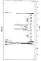
- One exemplary construction of the organic EL device according to the invention is shown in Fig. 1.
- the organic EL device comprises a hole injecting electrode 3, a hole injecting and transporting layer 4, a light emitting layer 5, an electron injecting and transporting layer 6 and an electron injecting electrode 7 in the described order.
- a color filter 8 a fluorescence conversion filter 9
- an organic EL device as mentioned above a sealing layer 10 and a cover 11 are stacked and formed on a glass substrate 2 in the described order, an organic EL color display is then obtained.
- the light emitting layer has functions of injecting holes and electrons, transporting them, and recombining holes and electrons to create excitons.
- the hole injecting and transporting layer has functions of facilitating injection of holes from the hole injecting electrode, providing stable transportation of holes and blocking electrons
- the electron injecting and transporting layer has functions of facilitating injection of electrons from the electron injecting electrode, providing stable transportation of electrons and blocking holes.
- the electron injecting and transporting layer and the hole injecting and transporting layer may be provided, if required, while care is taken of the magnitudes of the functions which the compound used for the light emitting layer has in injecting electrons, transporting electrons, injecting holes, and transporting holes.
- the hole or electron injecting and transporting layer may be dispensed with; that is, the light emitting layer may be allowed to function as a hole injecting and transporting layer or an electron injecting and transporting layer.
- both the hole injecting and transporting layer and the electron injecting and transporting layer may be dispensed with.
- the hole injecting and transporting layer and the electron injecting and transporting layer may be each separated into an injecting layer and a transporting layer.
- the thickness of the organic layer By controlling the thickness of the organic layer while care is taken of the carrier mobility or carrier density (determined depending on ionization potential and electron affinity) of the light emitting layer, electron injecting and transporting layer or hole injecting and transporting layer to be combined therewith, it is possible to freely determine the recombination/light emitting region. It is in turn possible to design the color of light to be emitted, and control emission luminance and spectra due to the interference effect between both electrode as well as the spatial distribution of light emission.
- the carrier mobility or carrier density determined depending on ionization potential and electron affinity
- the compound of the invention may be applied to any one of the hole injecting layer, hole transporting layer, light emitting layer, and hole injecting and transporting layer. Since the compound of the invention is excellent in the capability of injecting holes, however, it is preferably applied to the hole injecting layer or hole injecting and transporting layer, especially the hole injecting layer.
- the compound of the invention that has both the phenylenediamine skeleton and the diamine skeleton including a plurality of phenylene radicals such as a benzidine skeleton, it is possible to freely control ionization potential and carrier mobility without sacrifice of heat resistance and, hence, optimize hole injection efficiency depending on the material to be combined therewith.
- the hole injecting and transporting layer may be formed by the evaporation of the compound of the invention or the coating of a dispersion of the compound of the invention in a resin binder. Especially the evaporation of the compound of the invention yields a good enough amorphous film.
- the fluorescent material used for the light emitting layer may be selected from materials emitting fluorescence of longer wavelength. For instance, a sensible selection may be made from at least one fluorescent material used for the light emitting layer in combination with the compound of the invention. In such a case, too, the compound of the invention may be applied to the light emitting layer.
- the compound of the invention may be used.
- the compound of the invention has the phenylenediamine skeleton contributing to very strong donicity, and so is susceptible to interaction with the light emitting layer, resulting a drop of the intensity of fluorescence due to the formation of exciplexes, etc. This in turn offers problems such as a light emission efficiency drop, and a color purity drop due to the broadening of emission spectra, and so is undesired.
- the compound of the invention may be used as a hole transporting material.
- the hole injecting and transporting layer may be formed of a combination of more than one of hole injecting and transporting materials.
- hole injecting and transporting materials are laminated on ITO in the order of increasing ionization potential, for instance, in the order of a hole injecting layer and a hole transporting layer.
- a hole injecting material having a good thin film property so that a uniform thin film can be formed on the ITO surface having a varying hydrophilic nature. Since evaporation is utilized in the manufacture of devices, films as thin as about 1 to 10 nm can be formed in a uniform and pinhole-free state. If film thickness, refractive index, etc. are regulated, it is then possible to prevent an efficiency drop by controlling the color of light emitted and emission luminance or making use of interference light effects such as the spatial distribution of light emission.
- a triarylamine polymer having a benzidine skeleton alone and less susceptible to interaction with the light emitting material such as those set forth in JP-A's 63-295695, 5-234681 and 7-43564.
- the light emitting layer may contain a fluorescent material.
- the fluorescent material used herein may be at least one compound selected from compounds such as those disclosed in JP-A 63-264692, for instance, quinacridone, rubrene, and styryl dyes.
- Use may also be made of quinoline derivatives such as metal complex dyes containing 8-quinolinol or its derivative as ligands, for instance, tris(8-quinolinolato)aluminum, tetraphenylbutadiene, anthracene, perylene, coronene, and 12-phthaloperinone derivatives.
- Use may further be made of phenyanthracene derivatives disclosed in Japanese Patent Application No. 6-110569, and tetraarylethene derivatives disclosed in Japanese Patent Application 6-114456.
- the fluorescent compound is used in combination with a host substance capable of emitting light by itself; that is, it is preferable that the fluorescent compound is used as a dopant.
- the consent of the fluorescent compound in the light emitting layer is in the range of preferably 0.01 to 10% by weight, and especially 0.1 to 5% by weight.
- Quinolinolato complexes and aluminum complexes containing 8-quinolinol or its derivatives as ligands are preferred for the host substance.
- Such aluminum complexes are typically disclosed in JP-A's 63-264692, 3-255190, 5-70733, 5-258859, 6-215874, etc.
- Exemplary aluminum complexes include tris(8-quinolinolato)aluminum, bis(8-quinolinolato)magnesium, bis(benzo ⁇ f ⁇ -8-quinolinolato)zinc, bis(2-methyl-8-quinolinolato)aluminum oxide, tris(8-quinolinolato)indium, tris(5-methyl-8-quinolinolato)aluminum, 8-quinolinolatolithium, tris(5-chloro-8-quinolinolato)gallium, bis(5-chloro-8-quinolinolato)calcium, 5,7-dichloro-8-quinolinolatoaluminum, tris(5,7-dibromo-8-hydroxyquinolinolato)aluminum, and poly[zinc(II)-bis(8-hydroxy-5-quinolinyl)methane].
- Use may also be made of aluminum complexes containing other ligands in addition to 8-quinolinol or its derivatives, for instance, bis(2-methyl-8-quinolinolato)(phenolato) aluminum (III), bis(2-methyl-8-quinolinolato)(o-cresolato) aluminum (III), bis(2-methyl-8-qinolinolato)(m-cresolato) aluminum (III), bis(2-methyl-8-quinolinolato)(p-cresolato) aluminum (III), bis(2-methyl-8-quinolinolato)(o-phenyl-phenolato)aluminum (III), bis(2-methyl-8-quinolinolato) (m-phenylphenolato)aluminum (III), bis(2-methyl-8-quinolinolato) (p-phenylphenolato)aluminum (III), bis (2-methyl-8-quinolinolato)(2,3-dimethylphenolato)aluminum (III),
- phenylanthracene derivatives disclosed in Japanese Patent Application No. 6-110569 phenylanthracene derivatives disclosed in Japanese Patent Application No. 6-110569, tetraarylethene derivatives disclosed in Japanese Patent Application No. 6-114456, etc.
- the phenylanthracene derivatives are represented by the following formula (VIII): A 1 -L 1 -A 2
- a 1 and A 2 may be identical with or different from each other, and are each a monophenylanthryl or diphenylanthryl group.
- the monophenylanthryl or diphenylanthryl group represented by A 1 , and A 2 may, or may not, have a substituent.
- the substituent for instance, may be an alkyl, aryl, alkoxy, aryloxy or amino group which may have another substituent. Where is substituted by such a substituent is not critical in the invention. However, it is preferable that the phenyl group attached to the anthracene ring rather than the anthracene ring per se is substituted by such a substituent.
- the bond position of the phenyl group in the anthracene ring is the 9- or 10-position in the anthracene ring.
- L 1 stands for a single bond or an arylene group.
- the arylene group given by L 1 is preferably unsubstituted.
- the arylene group includes an ordinary arylene group such as a phenylene group, a biphenylene group, and an anthrylene group as well as two or more such arylene groups attached directly to each other.
- L 1 is preferably a single bond, and a p-phenylene or 4,4'-biphenylene group.
- L 1 may also include two or more such arylene groups as attached to each other via an alkylene group, -O-, -S- or -NR-where R is an alkyl or aryl group.
- R is an alkyl or aryl group.
- a methyl or ethyl group is mentioned for the alkyl group and a phenyl group is mentioned for the aryl group.
- Particular preference is given to the aryl group, for instance, a phenyl group as well as A 1 and A 2 .
- a phenyl group with A 1 or A 2 attached thereto may also be acceptable.
- Preferred for the alkylene group are a methylene group, an ethylene group or the like. Examples of such an arylene group are given below.
- Ar 1 , Ar 2 and Ar 3 may be identical with or different from one another, and are each an aromatic residue.
- Aromatic hydrocarbon groups (aryl groups), and aromatic heterocyclic groups, for instance, may be mentioned for the aromatic residues represented by Ar 1 , Ar 2 and Ar 3 .
- the aromatic hydrocarbon groups may monocyclic or polycyclic aromatic hydrocarbon groups, and include fused rings or ring combinations as well.
- Each aromatic hydrocarbon group has preferably 6 to 30 carbon atoms in all, and may have a substituent represented by an alkyl group, an aryl group, an alkoxy group, an aryloxy group, an amino group or the like.
- aromatic hydrocarbon groups include phenyl, alkylphenyl, alkoxyphenyl, arylphenyl, aryloxyphenyl, aminophenyl, biphenyl, naphthyl, anthryl, pyrenyl, and perylenyl groups.
- the aromatic heterocyclic groups are preferably those containing O, N, and S as a hetero-atom, and may each be a five- or six-membered ring. For instance, thienyl, furyl, pyrrolyl and pyridyl groups are mentioned.
- a phenyl group is particularly preferred for the aromatic group represented by Ar 1 , Ar 2 , and Ar 3 .
- n is an integer of preferably 2 to 6, and especially 2 to 4.
- L 2 is an n-valent aromatic residue. It is preferably a di- to hexa-valent, especially di- to tetra-valent residue derived from an aromatic hydrocarbon, an aromatic heterocyclic ring, an aromatic ether or an aromatic amine. This aromatic residue, which may have a substituent, is preferably unsubstituted.
- the light emitting layer is formed by using the compound of formula (IX) in combination with the aforesaid host material. It is also preferred that the light emitting layer is formed of a mixed layer of at least one compound capable of injecting and transporting holes with at least one compound capable of injecting and transporting electrons. Preferably in this case, a dopant is incorporated in the mixed layer.
- the content of the dopant compound in the mixed layer is in the range of preferably 0.01 to 20% by weight, and especially 0.1 to 15% by weight.
- each carrier migrates in the polarly prevailing substance, so making the injection of carriers having an opposite polarity unlikely to occur. This leads to an increase in the service life of the device due to less damage to the organic compound.
- the compound of formula (IX) in such a mixed layer, it is possible to vary the wavelength performance of light emission that the mixed layer itself possesses, thereby shifting the wavelength of light emission to a longer wavelength side and improving the intensity of light emission, and the stability of the device as well.
- the compound capable of injecting and transporting holes and the compound capable of injecting and transporting electrons, both used to form the mixed layer may be selected from compounds for the injection and transportation of holes and compounds for the injection and transportation of electrons.
- the compounds capable of injecting and transporting electrons it is preferable to use metal complexes containing quinoline derivatives, especially 8-quinolinol or its derivatives as ligands, in particular, tris(8-quinolinolato) aluminum (Alq 3 ). It is also preferable to use the aforesaid phenylanthracene derivatives, and tetraarylamine derivatives.
- amine derivatives having strong fluorescence for instance, hole transporting materials such as tetraphenyldiamine derivatives, styrylamine derivatives, and amine derivatives having an aromatic fused ring, as already mentioned.
- the mixing ratio is determined while the carrier mobility and carrier density are taken into consideration.
- the weight ratio between the compound capable of injecting and transporting holes and the compound capable of injecting and transporting electrons is of the order of 1/99 to 99/1, particularly 10/90 to 90/10, and more particularly 20/80 to 80/20.
- the thickness of the mixed layer must correspond to the thickness of a single molecular layer, and so is preferably less than the thickness of the organic compound layer. More specifically, the mixed layer has a thickness of preferably 1 to 85 nm, especially 5 to 60 nm, and more especially 5 to 50 nm.
- the mixed layer is formed by co-evaporation where the selected compounds are evaporated from different evaporation sources.
- the compounds to be mixed have identical or slightly different vapor pressures (evaporation temperatures), however, they may have previously been mixed together in the same evaporation boat for the subsequent evaporation.
- the compounds are uniformly mixed together in the mixed layer.
- the compounds in an archipelagic form may be present in the mixed layer.
- the light emitting layer may generally be formed at a given thickness by the evaporation of the organic fluorescent substance or coating a dispersion of the organic fluorescent substance in a resin binder.
- the electron injecting and transporting layer may be provided.
- the electron injecting and transporting layer there may be used quinoline derivatives such as organic metal complexes containing 8-quinolinol or its derivatives as ligands, for instance, tris(8-quinolinolato)aluminum (Alq 3 ), oxadiazole derivatives, perylene derivatives, pyridine derivatives, pyrimidine derivatives, quinoxaline derivative, diphenylquinone derivatives, and nitro-substituted fluorene derivatives.
- the electron injecting and transporting layer may also serve as a light emitting layer. In this case, it is preferable to use tris(8-quinolilato)aluminum, etc.
- the electron injecting and transporting layer may then be formed by evaporation or the like.
- the hole, and electron injecting and transporting layer may be formed of various organic compounds as disclosed in JP-A's 63-295695, 2-191694, 3-792 and so on.
- the hole injecting and transporting layer for instance, aromatic tertiary amines, hydrazone derivatives, carbazole derivatives, triazole derivatives, imidazole derivatives, and indole derivatives may be used.
- organic metal complex derivatives such as aluminum quinolinol, oxadiazole derivatives, pyridine derivatives, pyrimidine derivatives, quinoline derivatives, quinoxaline derivative, diphenylquinone derivatives, perylene derivatives and fluorene derivatives may be used.
- the compound of the invention When the compound of the invention is used for the light emitting layer, it is preferable to combine the compound of the invention with the aforesaid light emitting material unlikely to extinguish light due to their interaction.
- the compound of the invention emits strong blue fluorescence, and so can achieve a high-luminance light emitting device when combined with a material having little interaction therewith.
- the thickness of the light emitting layer, the hole injecting and transporting layer, and the electron injecting and transporting layer is not critical and varies with the design of recombination/light emitting region and a particular formation technique although it is usually of the order of preferably 5 to 500 nm, and especially 10 to 200 nm.
- the thickness of the hole injecting and transporting layers, and the electron injecting and transporting layer is equal to, or about 1/10 times to about 10 times as large as, the thickness of the light emitting layer although it depends on the design of the recombination/light emitting region.
- the injecting layer is at least 1 nm thick and the transporting layer is at least 1 nm and especially at least 20 nm thick.
- the upper limit on thickness is usually about 500 nm and especially about 100 nm for the injecting layer and about 500 nm for the transporting layer. The same film thickness applies when two injecting and transporting layers are provided.
- the thickness of the organic layer By controlling the thickness of the organic layer while care is taken of the carrier mobility or carrier density (determined depending on ionization potential and electron affinity) of the light emitting layer, electron injecting and transporting layer or hole injecting and transporting layer to be combined therewith, it is possible to freely determine the recombination/light emitting region. It is in turn possible to design the color of light to be emitted, and control emission luminance and spectra due to the interference effect between both electrode as well as the spatial distribution of light emission.
- the carrier mobility or carrier density determined depending on ionization potential and electron affinity
- the electron injecting electrode it is preferable to use a material having a low work function, for instance, Li, Na, K, Mg, Al, Ag or In, an alloy thereof, or an oxide or halide thereof. It is also preferred that the electron injecting electrode be formed of fine crystal grains, especially in an amorphous state.
- the electron injecting electrode has preferably a thickness of the order of 10 to 1,000 nm.
- the hole injecting electrode is preferably transparent or semitransparent. Since there is some limitation on the material of which the electron injecting electrode is formed as mentioned above, however, the material and thickness of the hole injecting electrode are preferably determined such that at least 80% of the light emitted transmits through it. For instance, it is preferable to use ITO (tin-doped indium oxide), IZO (zinc-doped indium oxide), SnO 2 , Ni, Au, Pt, Pd, and polypyrrole for the hole injecting electrode. It is also preferable that the hole injecting electrode has a thickness of the order of 10 to 500 nm.
- the driving voltage be low.
- an ITO of 10 to 30 ⁇ / ⁇ (with a thickness of 80 to 300 nm).
- the thickness and optical constant of the ITO may be designed such that high light extraction efficiency and high color purity are satisfied by the interference effect due to reflection at the ITO interface.
- an Al interconnection may be applied because the resistance of the ITO increases.
- transparent or translucent materials such as glasses, and resins are used for the substrate material because, in the illustrated embodiment, the emitted light is extracted or taken out of the substrate side.
- the substrate may be colored or otherwise provided with a color filter film, fluorescence conversion film or dielectric reflecting film for controlling the color of light emitted.
- a color filter employed with liquid crystal display devices may be used.
- an optical thin film such as a dielectric multilayer film may be used.
- the fluorescence conversion film absorbs light emitted from an EL device and gives out light from the phosphors contained therein for the color conversion of light emission, and is composed of three components, a binder, a fluorescent material and a light absorbing material.
- a fluorescent material having high fluorescent quantum efficiency and especially a fluorescent material having strong absorption in an EL light emission wavelength region.
- Laser dyes are suitable for the practice of the invention.
- rohodamine compounds perylene compounds, cyanine compounds, phthalocyanine compounds (including subphthalocyanine compounds, etc.), naphthaloimide compounds, fused cyclic hydrocarbon compounds, fused heterocyclic compounds, styryl compounds, and coumarin compounds.
- the binder it is basically preferable to make an appropriate selection from materials that do not extinguish fluorescence. It is particularly preferable to use a material that can be finely patterned by photolithography, printing or the like. It is also preferable to use a material that is not damaged during ITO film formation.
- the light absorbing material is used when light is not fully absorbed by the fluorescent material, and so may be dispensed with, if not required.
- the light absorbing material it is preferable to make a selection from materials that do not extinguish the fluorescence of the fluorescent material.
- vapor phase growth processes such as evaporation, and sputtering.
- the hole injecting and transporting layer, the light emitting layer, and the electron injecting and transporting layer it is preferable to use a vacuum evaporation technique which enables a homogeneous thin film to be obtained.
- a vacuum evaporation technique which enables a homogeneous thin film to be obtained.
- the vacuum evaporation process it is possible to obtain homogeneous thin films in an amorphous state or with a crystal grain diameter of at most 0.1 ⁇ m.
- the use of a thin film having a crystal grain diameter exceeding 0.1 ⁇ m results in non-uniform light emission. To avoid this, it is required to increase the driving voltage of the device; however, there is a striking drop of hole injection efficiency.
- an evaporation rate of the order of 0.01 to 1 nm/sec. is preferably applied at a degree of vacuum of up to 10 -5 Torr (10 -4 Pa). It is also preferable to form the layers continuously in vacuum. If the layers are continuously formed in vacuum, high properties are then obtained because the adsorption of impurities on the interface between the adjacent layers can be avoided. In addition, the driving voltage of the device can be lowered while the growth and occurrence of dark spots are inhibited.
- the EL device of the invention is generally of the DC drive type while it may be of the AC or pulse drive type.
- the applied voltage is generally of the order of 2 to 20 volts.
- HIM34 N,N'-diphenyl-N,N'-bis[N-phenyl-N-4-tolyl(4-aminophenyl)]benzidine referred to below as HIM34 was obtained as in synthesis example 1 with the exception that 4-iodotoluene was used in place of 3-iodotoluene.
- HIM38 N,N'-diphenyl-N,N'-bis[N-phenyl-N-4-tolyl(4-aminophenyl)]benzidine referred to below as HIM38 was obtained as in synthesis example 1 with the exception that 4-iodonaphthalene was used in place of 3-iodotoluene.
- HIM35 N,N'-diphenyl-N,N'-bis[N-phenyl-N-4-tolyl(4-aminophenyl)]benzidine referred to below as HIM35 was obtained as in synthesis example 1 with the exception that 3-iodobiphenyl was used in place of 3-iodotoluene.
- N,N'-diphenyl-N-(3-tolyl)-1,4-phenylenediamine was obtained.
- reaction vessel 17.5 grams of N,N'-diphenyl-N-3-tolylphenylenediamine and 32 grams of 1,4-diiodobenzene were heated together with 0.3 grams of activated copper powders, 50 grams of potassium carbonate and 50 ml of decalin at an oil bath temperature of 200°C for 24 hours in an Ar atmosphere. After the completion of the reaction, the reaction solution was filtrated with the addition of 100 ml of toluene thereto, thereby removing insolubles. The filtrate was washed with water, and dried over sodium sulfate. Following this, the solvent was removed by distillation from the filtrate.
- HIM74 N,N'-diphenyl-N,N'-bis[N-phenyl-N-[N-phenyl-N-4-tolyl(4-aminophenyl)](4-aminophenyl)]benzidine referred to below as HIM74 was obtained as in synthesis example 5 with the exception that 4-iodotoluene was used instead of 3-iodotoluene.
- HIM 78 N,N'-diphenyl-N,N'-bis ⁇ N-phenyl-N-[N-phenyl-N-1-naphthyl (4-aminophenyl)](4-aminophenyl) ⁇ benzidine referred to below as HIM 78 was obtained as in synthesis example 5 with the exception that 1-iodonaphthalene was used instead of 3-iodotoluene.
- reaction vessel 21 grams of N,N'-diphenyl-N-3-tolylphenylenediamine and 10 grams of 4,4''-diiodo-p-terphenyl were heated together with 0.3 grams of activated copper powders, 50 grams of potassium carbonate and 50 ml of decalin at an oil bath temperature of 200°C for 24 hours in an Ar atmosphere. After the completion of the reaction, the reaction solution was filtrated with the addition of 100 ml of toluene thereto for removal of insolubles, and the filtrate was washed with water and dried over sodium sulfate.
- a glass substrate having a 100 nm-thick ITO transparent electrode (a hole injecting electrode) was ultrasonically washed with neutral detergent, acetone, and ethanol, and then pulled up from boiling ethanol, followed by drying.
- This substrate was cleaned with UV/O 3 , and fixed to a substrate holder in a vacuum evaporation system, which was evacuated to a vacuum of 1 x 10 -6 Torr (10 -4 Pa).
- tris(quinolinolato)aluminum Alq 3
- Alq 3 tris(quinolinolato)aluminum
- MgAg (having a weight ratio of 10:1) was evaporated at a deposition rate of 0.2 nm/sec. to a thickness of 200 nm to form an electron injecting electrode. Finally, Al was evaporated to a thickness of 100 nm to form a protective layer, thereby obtaining an organic EL device.
- the half life of luminance was 500 hours (with an initial luminance of 2,030 cd/m 2 , an initial driving voltage of 6.55 V, and a driving voltage increase of 3.5 V).
- HIM34 compound No. 2
- HIM33 compound No. 3
- the half life of luminance was 800 hours (with an initial luminance of 2,040 cd/m 2 , an initial driving voltage of 6.59 V, and a driving voltage increase of 3.0 V).
- HIM38 compound No. 16
- HIM33 compound No. 3
- the half life of luminance was 1,600 hours (with an initial luminance of 1,923 cd/m 2 , an initial driving voltage of 6.59 V, and a driving voltage increase of 1.5 V).
- HIM73 compound No. 26
- HIM 33 compound No. 3
- the half life of luminance was 1,000 hours (with an initial luminance of 1,841 cd/m 2 , an initial driving voltage of 6.76 V, and a driving voltage increase of 2.5 V).
- HIM74 compound No. 25
- HIM33 compound No. 3
- the half life of luminance was 1,000 hours (with an initial luminance of 1,841 cd/m 2 , an initial driving voltage of 6.76 V, and a driving voltage increase of 1.5 V).
- a device was prepared as in example 1 with the exception that N,N'-diphenyl-N,N'-bis[N-phenyl-N-4-tolyl(4-aminophenyl)]benzidine (HIM35: compound No. 10) or N,N'-diphenyl-N,N'-bis ⁇ N-phenyl-N-[N-phenyl-N-1-naphthyl(4-aminophenyl)](4-aminophenyl) ⁇ benzidine (HIM78: compound No. 40) was used in place of the aforesaid HIM33 (compound No. 3). Equivalent results as in example 1 were obtained. Even with other exemplified compounds, equivalent results were obtained.
- a device was prepared as in example 1. Instead of the hole transporting layer of example 1, however, a hole transporting and light emitting layer was formed by mixing a hole transporting material TPD, rubrene, i.e., a light emitting material having such a structure as given below and aluminum quinolinol (Alq 3 ), i.e., an electron injecting material having such a structure as given below at a weight mixing ratio of 5:5:1 to form a mixed layer of 40 nm in thickness by means of triple co-evaporation. Thereafter, aluminum quinolinol (Alq 3 ) was evaporated to a thickness of 30 nm.
- TPD hole transporting material
- rubrene i.e., a light emitting material having such a structure as given below
- Al quinolinol (Alq 3 ) aluminum quinolinol
- the half life of luminance was 30,000 hours (2,350 cd/m 2 and a driving voltage increase of 1.0 V), and the half life was 10,000 hours or longer when the initial luminance was 300 cd/m 2 .
- the hole transporting layer of example 1 was formed of TPD alone, the thickness of the Alq 3 light emitting layer was changed to 10 nm, and a tetraphenylethene or phenylanthracene layer of 30 nm in thickness was interleaved between the hole transporting layer and the light emitting layer. Consequently, equivalent results as mentioned above were obtained.
- a device was prepared as in example 1 with the exception that 4,4',4''-tris[-N-(-3-methylphenyl)-N-phenylamino] triphenylamine (MTDATA) having such a structure as given below was used in place of HIM33 (compound No. 3).
- MTDATA 4,4',4''-tris[-N-(-3-methylphenyl)-N-phenylamino] triphenylamine
- a device was prepared as in example 1 with the exception that copper phthalocyanine having such a structure as given below and a thickness of 10 nm was used for HIM33 (compound No. 3).
- a glass substrate having a 100 nm-thick ITO transparent electrode (a hole injecting electrode) was ultrasonically washed with neutral detergent, acetone, and ethanol, and then pulled up from boiling ethanol, followed by drying.
- This substrate was cleaned with UV/O 3 , and fixed to a substrate holder in a vacuum evaporation system, which was evacuated to a vacuum of 1 x 10 -6 Torr (10 -4 Pa).
- Al was evaporated at a deposition rate of 2 nm/sec. to a thickness of 200 nm to form an electron injecting electrode, thereby obtaining a single layer device.
- the Hole mobility was found to be 2.7 x 10 -3 cm 2 /Vs as measured by the time-of-flight method. This value is at least twice as high as that of a general hole injecting and transporting material TPD, i.e., N,N'-bis(3-methylphenyl)-N,N'-diphenyl-1,1'-biphenyl-4,4'-diamine.
- a device was obtained as in example 9 with the exception that the aforesaid MTDATA was used in place of HIM34.
- the device of the invention makes it possible to obtain a much higher current density at the same voltage because of its enhanced hole supply efficiency.
- An organic EL device was prepared as in example 2 with the exception that the thickness of the hole injecting layer containing N,N'-diphenyl-N,N'-bis[N-phenyl-N-4-tolyl(4-aminophenyl)]benzidine (HIM34: compound No. 2) was changed from 50 nm to 300 nm.
- the half life of luminance was 1,500 hours (with an initial luminance of 1,800 cd/m 2 , an initial driving voltage of 7.6 V, and a driving voltage increase of 3.0 V).
- the organic EL device constructed using the compound of the invention is substantially free from a driving voltage increase or a luminance drop and a current leakage with neither development nor growth of local non-emitting spots while it is driven, and so is capable of emitting light with high luminance, and high reliability such as high heat resistance.
- the optimum work function can be imparted to a hole injecting electrode or an organic material combined therewith, so that a device emitting light continuously with high reliability can be achieved.
Applications Claiming Priority (3)
| Application Number | Priority Date | Filing Date | Title |
|---|---|---|---|
| JP35841696 | 1996-12-28 | ||
| JP358416/96 | 1996-12-28 | ||
| PCT/JP1997/004904 WO1998030071A1 (fr) | 1996-12-28 | 1997-12-26 | Elements electroluminescents organiques |
Publications (4)
| Publication Number | Publication Date |
|---|---|
| EP0891121A1 true EP0891121A1 (fr) | 1999-01-13 |
| EP0891121A4 EP0891121A4 (fr) | 2003-01-02 |
| EP0891121B1 EP0891121B1 (fr) | 2012-09-26 |
| EP0891121B8 EP0891121B8 (fr) | 2013-01-02 |
Family
ID=18459187
Family Applications (1)
| Application Number | Title | Priority Date | Filing Date |
|---|---|---|---|
| EP97950436A Expired - Lifetime EP0891121B8 (fr) | 1996-12-28 | 1997-12-26 | Elements electroluminescents organiques |
Country Status (4)
| Country | Link |
|---|---|
| US (3) | US6344283B1 (fr) |
| EP (1) | EP0891121B8 (fr) |
| JP (3) | JP3654909B2 (fr) |
| WO (1) | WO1998030071A1 (fr) |
Cited By (168)
| Publication number | Priority date | Publication date | Assignee | Title |
|---|---|---|---|---|
| EP1030382A2 (fr) * | 1999-02-18 | 2000-08-23 | Pioneer Corporation | Dispositif organique électroluminescent et procédé de fabrication |
| EP1029909A1 (fr) * | 1998-09-09 | 2000-08-23 | Idemitsu Kosan Co., Ltd. | Dispositif organique electroluminescent et derive de phenylenediamine |
| WO2001023344A1 (fr) * | 1999-09-30 | 2001-04-05 | Idemitsu Kosan Co., Ltd. | Compose d'amine et element electroluminescent organique utilisant ce compose |
| WO2002094965A1 (fr) * | 2001-05-24 | 2002-11-28 | Idemitsu Kosan Co., Ltd. | Élément électroluminescent organique |
| EP1311009A2 (fr) * | 2001-11-08 | 2003-05-14 | Xerox Corporation | Dispositif luminescent organique |
| US6610455B1 (en) | 2002-01-30 | 2003-08-26 | Eastman Kodak Company | Making electroluminscent display devices |
| WO2003074628A1 (fr) * | 2002-03-04 | 2003-09-12 | Cdt Oxford Limited | Compositions phosphorescentes et dispositifs organiques electroluminescents les contenant |
| EP1367677A2 (fr) | 2002-05-28 | 2003-12-03 | Eastman Kodak Company | Dispositif d'éclairage avec une oled flexible comme source lumineuse |
| EP1443093A1 (fr) * | 2003-01-29 | 2004-08-04 | Samsung SDI Co., Ltd. | Composés moléculaires chimiques capable d'émettre de la photoluminescence comprenant des structures électroniques déplaçables et leur utilisation dans des dispositifs d'affichage photoluminescents effaçables |
| WO2004099338A2 (fr) * | 2002-09-25 | 2004-11-18 | 3M Innovative Properties Company | Compositions organiques electroluminescentes |
| US6849345B2 (en) | 2001-09-28 | 2005-02-01 | Eastman Kodak Company | Organic electroluminescent devices with high luminance |
| US6872472B2 (en) | 2002-02-15 | 2005-03-29 | Eastman Kodak Company | Providing an organic electroluminescent device having stacked electroluminescent units |
| US6890627B2 (en) | 2002-08-02 | 2005-05-10 | Eastman Kodak Company | Laser thermal transfer from a donor element containing a hole-transporting layer |
| US6919140B2 (en) | 2003-07-10 | 2005-07-19 | Eastman Kodak Company | Organic electroluminescent devices with high luminance |
| US6939660B2 (en) | 2002-08-02 | 2005-09-06 | Eastman Kodak Company | Laser thermal transfer donor including a separate dopant layer |
| WO2006034028A2 (fr) | 2004-09-21 | 2006-03-30 | Eastman Kodak Company | Alimentation en matiere particulaire d'une source de vaporisation |
| EP1666561A1 (fr) * | 1998-12-28 | 2006-06-07 | Idemitsu Kosan Company Limited | Elément électroluminescent organique |
| US7094902B2 (en) | 2002-09-25 | 2006-08-22 | 3M Innovative Properties Company | Electroactive polymers |
| US7192657B2 (en) | 2003-04-15 | 2007-03-20 | 3M Innovative Properties Company | Ethynyl containing electron transport dyes and compositions |
| US7221332B2 (en) | 2003-12-19 | 2007-05-22 | Eastman Kodak Company | 3D stereo OLED display |
| US7241512B2 (en) | 2002-04-19 | 2007-07-10 | 3M Innovative Properties Company | Electroluminescent materials and methods of manufacture and use |
| US7271406B2 (en) | 2003-04-15 | 2007-09-18 | 3M Innovative Properties Company | Electron transport agents for organic electronic devices |
| US7282275B2 (en) | 2002-04-19 | 2007-10-16 | 3M Innovative Properties Company | Materials for organic electronic devices |
| US7402343B2 (en) | 2003-01-29 | 2008-07-22 | Samsung Sdi Co., Ltd. | Molecular chemical compounds with structures allowing electron displacement and capable of emitting photoluminescent radiation, and photoluminescence quenching device employing the same |
| EP2161272A1 (fr) | 2008-09-05 | 2010-03-10 | Basf Se | Phénanthrolines |
| US7732811B2 (en) | 2006-12-04 | 2010-06-08 | Semiconductor Energy Laboratory Co., Ltd. | Light-emitting element, light-emitting device, and electronic device |
| DE102009005746A1 (de) | 2009-01-23 | 2010-07-29 | Merck Patent Gmbh | Materialien für organische Elektrolumineszenzvorrichtungen |
| WO2010094378A1 (fr) | 2009-02-17 | 2010-08-26 | Merck Patent Gmbh | Dispositif électronique organique |
| US7799439B2 (en) | 2006-01-25 | 2010-09-21 | Global Oled Technology Llc | Fluorocarbon electrode modification layer |
| WO2010108579A1 (fr) | 2009-03-23 | 2010-09-30 | Merck Patent Gmbh | Dispositif électroluminescent organique |
| WO2010114749A1 (fr) | 2009-04-03 | 2010-10-07 | Global Oled Technology Llc | Delo blanche en tandem à transfert d'électrons efficace |
| EP2239352A2 (fr) | 2004-09-21 | 2010-10-13 | Global OLED Technology LLC | Fourniture d'un matériau à particules dans une zone de vaporisation |
| DE102009017064A1 (de) | 2009-04-09 | 2010-10-14 | Merck Patent Gmbh | Organische Elektrolumineszenzvorrichtung |
| WO2010149259A2 (fr) | 2009-06-22 | 2010-12-29 | Merck Patent Gmbh | Formulation conductrice |
| EP2276089A2 (fr) | 2004-07-27 | 2011-01-19 | Global OLED Technology LLC | Absorbeur d'humidité pour un dispositif OLED à émission par le haut |
| WO2011015265A2 (fr) | 2009-08-04 | 2011-02-10 | Merck Patent Gmbh | Dispositifs électroniques comprenant des hydrocarbures polycycliques |
| US7893427B2 (en) | 2004-07-23 | 2011-02-22 | Semiconductor Energy Laboratory Co., Ltd. | Light emitting element and light emitting device using the same |
| DE102009041289A1 (de) | 2009-09-16 | 2011-03-17 | Merck Patent Gmbh | Organische Elektrolumineszenzvorrichtung |
| US7911133B2 (en) | 2007-05-10 | 2011-03-22 | Global Oled Technology Llc | Electroluminescent device having improved light output |
| WO2011032686A1 (fr) | 2009-09-16 | 2011-03-24 | Merck Patent Gmbh | Formulations pour la fabrication de dispositifs électroniques |
| DE102009042680A1 (de) | 2009-09-23 | 2011-03-24 | Merck Patent Gmbh | Organische Elektrolumineszenzvorrichtung |
| WO2011035836A1 (fr) | 2009-09-23 | 2011-03-31 | Merck Patent Gmbh | Matériaux pour dispositifs électroniques |
| US7931975B2 (en) | 2008-11-07 | 2011-04-26 | Global Oled Technology Llc | Electroluminescent device containing a flouranthene compound |
| DE102009053191A1 (de) | 2009-11-06 | 2011-05-12 | Merck Patent Gmbh | Materialien für elektronische Vorrichtungen |
| DE102009052428A1 (de) | 2009-11-10 | 2011-05-12 | Merck Patent Gmbh | Verbindung für elektronische Vorrichtungen |
| US7947974B2 (en) | 2008-03-25 | 2011-05-24 | Global Oled Technology Llc | OLED device with hole-transport and electron-transport materials |
| US7968215B2 (en) | 2008-12-09 | 2011-06-28 | Global Oled Technology Llc | OLED device with cyclobutene electron injection materials |
| WO2011076326A1 (fr) | 2009-12-22 | 2011-06-30 | Merck Patent Gmbh | Surfactants fonctionnels électroluminescents |
| WO2011076314A1 (fr) | 2009-12-22 | 2011-06-30 | Merck Patent Gmbh | Formulations électroluminescentes |
| WO2011076324A1 (fr) | 2009-12-23 | 2011-06-30 | Merck Patent Gmbh | Compositions comprenant des composés semi-conducteurs organiques |
| WO2011076380A1 (fr) | 2009-12-23 | 2011-06-30 | Merck Patent Gmbh | Composition pour la préparation de dispositifs électroniques organiques (oe) |
| WO2011076323A1 (fr) | 2009-12-22 | 2011-06-30 | Merck Patent Gmbh | Formulations comprenant des matériaux fonctionnels à phases séparées |
| EP2355198A1 (fr) | 2006-05-08 | 2011-08-10 | Global OLED Technology LLC | Couche d'njection d'électrons pour OLED |
| DE102010010481A1 (de) | 2010-03-06 | 2011-09-08 | Merck Patent Gmbh | Organische Elektrolumineszenzvorrichtung |
| US8016631B2 (en) | 2007-11-16 | 2011-09-13 | Global Oled Technology Llc | Desiccant sealing arrangement for OLED devices |
| WO2011110277A1 (fr) | 2010-03-11 | 2011-09-15 | Merck Patent Gmbh | Fibres en thérapie et cosmétique |
| WO2011110276A1 (fr) | 2010-03-09 | 2011-09-15 | Merck Patent Gmbh | Matériaux pour dispositifs électroniques |
| WO2011110275A2 (fr) | 2010-03-11 | 2011-09-15 | Merck Patent Gmbh | Fibres rayonnantes |
| US8034465B2 (en) | 2007-06-20 | 2011-10-11 | Global Oled Technology Llc | Phosphorescent oled having double exciton-blocking layers |
| WO2011128035A1 (fr) | 2010-04-12 | 2011-10-20 | Merck Patent Gmbh | Composition et procédé pour la préparation de dispositifs électroniques organiques |
| WO2011128034A1 (fr) | 2010-04-12 | 2011-10-20 | Merck Patent Gmbh | Composition ayant des performances améliorées |
| WO2011134458A1 (fr) * | 2010-04-27 | 2011-11-03 | Novaled Ag | Matériau semi-conducteur organique et composant électronique |
| US8053979B2 (en) | 1999-09-24 | 2011-11-08 | Semiconductor Energy Laboratory Co., Ltd. | Light-emitting organic compound with improved reliability |
| WO2011137922A1 (fr) | 2010-05-03 | 2011-11-10 | Merck Patent Gmbh | Formulations et dispositifs électroniques |
| US8057916B2 (en) | 2005-04-20 | 2011-11-15 | Global Oled Technology, Llc. | OLED device with improved performance |
| DE102010020044A1 (de) | 2010-05-11 | 2011-11-17 | Merck Patent Gmbh | Organische Elektrolumineszenzvorrichtung |
| WO2011147523A1 (fr) | 2010-05-27 | 2011-12-01 | Merck Patent Gmbh | Formulation et procédé pour la préparation de dispositifs électroniques organiques |
| WO2011147522A1 (fr) | 2010-05-27 | 2011-12-01 | Merck Patent Gmbh | Composition comprenant des points quantiques |
| US8076009B2 (en) | 2007-10-26 | 2011-12-13 | Global Oled Technology, Llc. | OLED device with fluoranthene electron transport materials |
| US8088500B2 (en) | 2008-11-12 | 2012-01-03 | Global Oled Technology Llc | OLED device with fluoranthene electron injection materials |
| US8102114B2 (en) | 2009-02-27 | 2012-01-24 | Global Oled Technology, Llc. | Method of manufacturing an inverted bottom-emitting OLED device |
| WO2012013270A1 (fr) | 2010-07-26 | 2012-02-02 | Merck Patent Gmbh | Nanocristaux utilisés dans des dispositifs |
| US8129039B2 (en) | 2007-10-26 | 2012-03-06 | Global Oled Technology, Llc | Phosphorescent OLED device with certain fluoranthene host |
| US8147989B2 (en) | 2009-02-27 | 2012-04-03 | Global Oled Technology Llc | OLED device with stabilized green light-emitting layer |
| DE102010048074A1 (de) | 2010-10-09 | 2012-04-12 | Merck Patent Gmbh | Materialien für elektronische Vorrichtungen |
| WO2012048780A1 (fr) | 2010-10-15 | 2012-04-19 | Merck Patent Gmbh | Composés pour dispositifs électroniques |
| US8202630B2 (en) | 2004-11-05 | 2012-06-19 | Semiconductor Energy Laboratory Co., Ltd. | Light emitting element and light emitting device using the same |
| US8206842B2 (en) | 2009-04-06 | 2012-06-26 | Global Oled Technology Llc | Organic element for electroluminescent devices |
| WO2012084114A1 (fr) | 2010-12-23 | 2012-06-28 | Merck Patent Gmbh | Dispositif électroluminescent organique |
| US8216697B2 (en) | 2009-02-13 | 2012-07-10 | Global Oled Technology Llc | OLED with fluoranthene-macrocyclic materials |
| WO2012095143A1 (fr) | 2011-01-13 | 2012-07-19 | Merck Patent Gmbh | Composés pour des dispositifs électroluminescents organiques |
| US8247088B2 (en) | 2008-08-28 | 2012-08-21 | Global Oled Technology Llc | Emitting complex for electroluminescent devices |
| WO2012110178A1 (fr) | 2011-02-14 | 2012-08-23 | Merck Patent Gmbh | Dispositif et procédé de traitement de cellules et de tissu cellulaire |
| US8253126B2 (en) | 1999-12-31 | 2012-08-28 | Lg Chem. Ltd. | Organic electronic device |
| EP2498317A2 (fr) | 2007-07-25 | 2012-09-12 | Global OLED Technology LLC | Prévention d'un transfert de contrainte dans des composants d'affichage OLED |
| WO2012126566A1 (fr) | 2011-03-24 | 2012-09-27 | Merck Patent Gmbh | Matériaux fonctionnels ioniques organiques |
| US8293921B2 (en) | 2009-03-31 | 2012-10-23 | Semiconductor Energy Laboratory Co., Ltd. | Triazole derivative, and light-emitting element, light-emitting device, lighting device, and electronic device using triazole derivative |
| WO2012149992A1 (fr) | 2011-05-04 | 2012-11-08 | Merck Patent Gmbh | Dispositif de conservation de produits frais |
| WO2012152366A1 (fr) | 2011-05-12 | 2012-11-15 | Merck Patent Gmbh | Composés ioniques organiques, compositions et dispositifs électroniques |
| US8324800B2 (en) | 2008-06-12 | 2012-12-04 | Global Oled Technology Llc | Phosphorescent OLED device with mixed hosts |
| WO2012163464A1 (fr) | 2011-06-01 | 2012-12-06 | Merck Patent Gmbh | Tft ambipolaires hybrides |
| US8334061B2 (en) | 2009-03-31 | 2012-12-18 | Semiconductor Energy Laboratory Co., Ltd. | Heterocyclic compound, and light-emitting element, light-emitting device, lighting device, and electronic appliance using heterocyclic compound |
| WO2012171609A1 (fr) | 2011-06-17 | 2012-12-20 | Merck Patent Gmbh | Matières pour dispositifs électroluminescents organiques |
| US8343639B2 (en) | 2008-09-05 | 2013-01-01 | Semiconductor Energy Laboratory Co., Ltd. | Organic semiconductor material and light-emitting element, light-emitting device, lighting system, and electronic device using the same |
| WO2013013754A1 (fr) | 2011-07-25 | 2013-01-31 | Merck Patent Gmbh | Copolymères ayant des chaînes latérales fonctionnalisées |
| TWI387391B (zh) * | 2009-03-04 | 2013-02-21 | Chung Shan Inst Of Science | 有機發光元件之製造方法 |
| TWI387394B (zh) * | 2009-03-04 | 2013-02-21 | Chung Shan Inst Of Science | 有機電激發光元件及其製造方法 |
| DE102012016192A1 (de) | 2011-08-19 | 2013-02-21 | Merck Patent Gmbh | Neue Materialien für organische Elektrolumineszenzvorrichtungen |
| WO2013026515A1 (fr) | 2011-08-22 | 2013-02-28 | Merck Patent Gmbh | Dispositif électroluminescent organique |
| WO2013050101A1 (fr) | 2011-10-06 | 2013-04-11 | Merck Patent Gmbh | Dispositif électroluminescents organiques |
| US8431242B2 (en) | 2007-10-26 | 2013-04-30 | Global Oled Technology, Llc. | OLED device with certain fluoranthene host |
| DE102011117422A1 (de) | 2011-10-28 | 2013-05-02 | Merck Patent Gmbh | Hyperverzweigte Polymere, Verfahren zu deren Herstellung sowie deren Verwendung in elektronischen Vorrichtungen |
| DE102012022880A1 (de) | 2011-12-22 | 2013-06-27 | Merck Patent Gmbh | Elektronische Vorrichtungen enthaltend organische Schichten |
| US8507896B2 (en) | 2008-03-11 | 2013-08-13 | Merck Patent Gmbh | Compounds having electroluminescent or electron transport properties |
| US8628862B2 (en) | 2007-09-20 | 2014-01-14 | Basf Se | Electroluminescent device |
| US8642188B2 (en) | 2006-12-22 | 2014-02-04 | Merck Patent Gmbh | Phenanthroline compounds and electroluminescent devices using the same |
| WO2014044344A1 (fr) | 2012-09-18 | 2014-03-27 | Merck Patent Gmbh | Matériaux pour dispositifs électroniques |
| US8771843B2 (en) | 2010-08-27 | 2014-07-08 | Semiconductor Energy Laboratory Co., Ltd. | Fluorene derivative, organic compound, and light-emitting element, light-emitting device, and electronic device using the compound |
| EP2752866A1 (fr) | 2002-08-20 | 2014-07-09 | Global OLED Technology LLC | Dispositif d'affichage de couleur a diode organique électroluminescent a durée de vie étenduée |
| US8795855B2 (en) | 2007-01-30 | 2014-08-05 | Global Oled Technology Llc | OLEDs having high efficiency and excellent lifetime |
| WO2014167286A2 (fr) | 2013-04-09 | 2014-10-16 | Power Oleds Limited | Composés hétérocycliques et leur utilisation dans des dispositifs électro-optiques ou opto-électroniques |
| US8877350B2 (en) | 2007-12-11 | 2014-11-04 | Global Oled Technology Llc | White OLED with two blue light-emitting layers |
| US8883325B2 (en) | 2006-12-29 | 2014-11-11 | Merck Patent Gmbh | Electroluminescent device using azomethine-lithium-complex as electron injection layer |
| US8900722B2 (en) | 2007-11-29 | 2014-12-02 | Global Oled Technology Llc | OLED device employing alkali metal cluster compounds |
| US8951443B2 (en) | 2009-07-31 | 2015-02-10 | Novaled Ag | Organic semiconducting material and electronic component |
| US8993125B2 (en) | 2010-05-21 | 2015-03-31 | Semiconductor Energy Laboratory Co., Ltd. | Triazole derivative, and light-emitting element, light-emitting device, electronic device and lighting device using the triazole derivative |
| US9028979B2 (en) | 2009-06-18 | 2015-05-12 | Basf Se | Phenanthroazole compounds as hole transporting materials for electro luminescent devices |
| US9040170B2 (en) | 2004-09-20 | 2015-05-26 | Global Oled Technology Llc | Electroluminescent device with quinazoline complex emitter |
| WO2015082037A1 (fr) | 2013-12-06 | 2015-06-11 | Merck Patent Gmbh | Compositions contenant un liant polymère qui comprend des unités d'ester d'acide acrylique et/ou méthacrylique |
| US9252383B2 (en) | 2006-07-26 | 2016-02-02 | Merck Patent Gmbh | Cathode coating |
| WO2016034262A1 (fr) | 2014-09-05 | 2016-03-10 | Merck Patent Gmbh | Formulations et dispositifs électroniques |
| WO2016107663A1 (fr) | 2014-12-30 | 2016-07-07 | Merck Patent Gmbh | Formulations et dispositifs électroniques |
| WO2016120007A1 (fr) | 2015-01-30 | 2016-08-04 | Merck Patent Gmbh | Formulations à faible teneur en particules |
| WO2016155866A1 (fr) | 2015-03-30 | 2016-10-06 | Merck Patent Gmbh | Formulation de materiau fonctionnel organique comprenant un solvant siloxane |
| EP3101691A1 (fr) | 2002-12-16 | 2016-12-07 | Global OLED Technology LLC | Affichage oled couleur avec une efficacité de puissance améliorée |
| WO2016198141A1 (fr) | 2015-06-12 | 2016-12-15 | Merck Patent Gmbh | Esters contenant des cycles non aromatiques en tant que solvants pour des formulations de diodes électroluminescentes organiques (oled) |
| WO2017008883A1 (fr) | 2015-07-15 | 2017-01-19 | Merck Patent Gmbh | Composition comprenant des composés semi-conducteurs organiques |
| WO2017036572A1 (fr) | 2015-08-28 | 2017-03-09 | Merck Patent Gmbh | Formulation d'un matériau fonctionnel organique comprenant un solvant contenant un groupe époxy |
| US9666826B2 (en) | 2005-11-30 | 2017-05-30 | Global Oled Technology Llc | Electroluminescent device including an anthracene derivative |
| WO2017097391A1 (fr) | 2015-12-10 | 2017-06-15 | Merck Patent Gmbh | Formulations contenant des cétones comprenant des cycles non aromatiques |
| WO2017102052A1 (fr) | 2015-12-16 | 2017-06-22 | Merck Patent Gmbh | Formulations contenant un solvant solide |
| WO2017102048A1 (fr) | 2015-12-15 | 2017-06-22 | Merck Patent Gmbh | Esters contenant des groupes aromatiques comme solvants pour formulations électroniques organiques |
| WO2017102049A1 (fr) | 2015-12-16 | 2017-06-22 | Merck Patent Gmbh | Formulations contenant un mélange d'au moins deux solvants différents |
| WO2017140404A1 (fr) | 2016-02-17 | 2017-08-24 | Merck Patent Gmbh | Formulation de substance fonctionnelle organique |
| WO2017157783A1 (fr) | 2016-03-15 | 2017-09-21 | Merck Patent Gmbh | Contenant comprenant une formulation contenant au moins un semiconducteur organique |
| WO2017216128A1 (fr) | 2016-06-17 | 2017-12-21 | Merck Patent Gmbh | Formulation de matiere fonctionnelle organique |
| WO2017216129A1 (fr) | 2016-06-16 | 2017-12-21 | Merck Patent Gmbh | Formulation de matiere fonctionnelle organique |
| WO2018001928A1 (fr) | 2016-06-28 | 2018-01-04 | Merck Patent Gmbh | Formulation de matériau fonctionnel organique |
| WO2018024719A1 (fr) | 2016-08-04 | 2018-02-08 | Merck Patent Gmbh | Formulation d'une matière fonctionnelle organique |
| US9960360B2 (en) | 2006-06-22 | 2018-05-01 | Idemitsu Kosan Co., Ltd. | Organic electroluminescent device using aryl amine derivative containing heterocycle |
| WO2018077662A1 (fr) | 2016-10-31 | 2018-05-03 | Merck Patent Gmbh | Formulation d'une matière organique fonctionnelle |
| WO2018077660A1 (fr) | 2016-10-31 | 2018-05-03 | Merck Patent Gmbh | Formulation d'un matériau fonctionnel organique |
| WO2018104202A1 (fr) | 2016-12-06 | 2018-06-14 | Merck Patent Gmbh | Procédé de préparation d'un dispositif électronique |
| WO2018108760A1 (fr) | 2016-12-13 | 2018-06-21 | Merck Patent Gmbh | Formulation d'un matériau fonctionnel organique |
| WO2018114883A1 (fr) | 2016-12-22 | 2018-06-28 | Merck Patent Gmbh | Mélanges comprenant au moins deux composés organo-fonctionnels |
| WO2018138319A1 (fr) | 2017-01-30 | 2018-08-02 | Merck Patent Gmbh | Procédé de formation d'un élément à électroluminescence (el) organique |
| WO2018138318A1 (fr) | 2017-01-30 | 2018-08-02 | Merck Patent Gmbh | Procédé de formation d'un élément organique d'un dispositif électronique |
| WO2018178136A1 (fr) | 2017-03-31 | 2018-10-04 | Merck Patent Gmbh | Procédé d'impression pour une diode électroluminescente organique (oled) |
| WO2018189050A1 (fr) | 2017-04-10 | 2018-10-18 | Merck Patent Gmbh | Formulation d'un matériau fonctionnel organique |
| WO2018202603A1 (fr) | 2017-05-03 | 2018-11-08 | Merck Patent Gmbh | Formulation d'un matériau fonctionnel organique |
| WO2019002198A1 (fr) | 2017-06-26 | 2019-01-03 | Merck Patent Gmbh | Mélanges homogènes |
| WO2019007823A1 (fr) | 2017-07-03 | 2019-01-10 | Merck Patent Gmbh | Formulations à faible teneur en impuretés de type phénol |
| WO2019016184A1 (fr) | 2017-07-18 | 2019-01-24 | Merck Patent Gmbh | Formulation d'un matériau fonctionnel organique |
| WO2019115573A1 (fr) | 2017-12-15 | 2019-06-20 | Merck Patent Gmbh | Formulation d'un matériau fonctionnel organique |
| WO2019162483A1 (fr) | 2018-02-26 | 2019-08-29 | Merck Patent Gmbh | Formulation d'un matériau fonctionnel organique |
| WO2019238782A1 (fr) | 2018-06-15 | 2019-12-19 | Merck Patent Gmbh | Formulation d'un matériau fonctionnel organique |
| US10593886B2 (en) | 2013-08-25 | 2020-03-17 | Molecular Glasses, Inc. | OLED devices with improved lifetime using non-crystallizable molecular glass mixture hosts |
| WO2020064582A1 (fr) | 2018-09-24 | 2020-04-02 | Merck Patent Gmbh | Procédé de production de granulat |
| WO2020094538A1 (fr) | 2018-11-06 | 2020-05-14 | Merck Patent Gmbh | Procédé de formation d'un élément organique d'un dispositif électronique |
| WO2020178230A1 (fr) | 2019-03-04 | 2020-09-10 | Merck Patent Gmbh | Ligands pour matériaux nanométriques |
| WO2021213917A1 (fr) | 2020-04-21 | 2021-10-28 | Merck Patent Gmbh | Émulsions comprenant des matériaux fonctionnels organiques |
| WO2021259824A1 (fr) | 2020-06-23 | 2021-12-30 | Merck Patent Gmbh | Procédé de production d'un mélange |
| WO2022122607A1 (fr) | 2020-12-08 | 2022-06-16 | Merck Patent Gmbh | Système d'encre et procédé d'impression à jet d'encre |
| WO2022243403A1 (fr) | 2021-05-21 | 2022-11-24 | Merck Patent Gmbh | Procédé de purification continue d'au moins un matériau fonctionnel et dispositif de purification continue d'au moins un matériau fonctionnel |
| WO2023012084A1 (fr) | 2021-08-02 | 2023-02-09 | Merck Patent Gmbh | Procédé d'impression par combinaison d'encres |
| WO2023031073A1 (fr) | 2021-08-31 | 2023-03-09 | Merck Patent Gmbh | Composition |
| WO2023057327A1 (fr) | 2021-10-05 | 2023-04-13 | Merck Patent Gmbh | Procédé de formation d'un élément organique d'un dispositif électronique |
| WO2023237458A1 (fr) | 2022-06-07 | 2023-12-14 | Merck Patent Gmbh | Procédé d'impression d'une couche fonctionnelle d'un dispositif électronique par combinaison d'encres |
Families Citing this family (42)
| Publication number | Priority date | Publication date | Assignee | Title |
|---|---|---|---|---|
| JP3654909B2 (ja) * | 1996-12-28 | 2005-06-02 | Tdk株式会社 | 有機el素子 |
| JP4542646B2 (ja) * | 1998-09-09 | 2010-09-15 | 出光興産株式会社 | 有機エレクトロルミネッセンス素子およびフェニレンジアミン誘導体 |
| JP4718670B2 (ja) * | 1999-09-24 | 2011-07-06 | 株式会社半導体エネルギー研究所 | El表示装置 |
| JP3793537B2 (ja) * | 1999-12-20 | 2006-07-05 | 松下電器産業株式会社 | 薄膜el素子 |
| US6803720B2 (en) * | 2000-12-15 | 2004-10-12 | Universal Display Corporation | Highly stable and efficient OLEDs with a phosphorescent-doped mixed layer architecture |
| CN100428524C (zh) * | 2001-06-15 | 2008-10-22 | 佳能株式会社 | 有机电致发光元件 |
| JP5010076B2 (ja) * | 2001-08-01 | 2012-08-29 | 三井化学株式会社 | 有機電界発光素子 |
| GB0220080D0 (en) * | 2002-08-29 | 2002-10-09 | Isis Innovation | Blended dendrimers |
| JP4142404B2 (ja) * | 2002-11-06 | 2008-09-03 | 出光興産株式会社 | 芳香族アミン誘導体及びそれを用いた有機エレクトロルミネッセンス素子 |
| US6869698B2 (en) * | 2002-12-04 | 2005-03-22 | Canon Kabushiki Kaisha | Organic light-emitting device using paracyclophane |
| JP2004262761A (ja) * | 2003-01-16 | 2004-09-24 | Idemitsu Kosan Co Ltd | 芳香族アミン誘導体及びそれを用いた有機エレクトロルミネッセンス素子 |
| JP4682042B2 (ja) * | 2003-12-26 | 2011-05-11 | 保土谷化学工業株式会社 | テトラミン化合物および有機el素子 |
| JP4587703B2 (ja) * | 2004-05-07 | 2010-11-24 | ケミプロ化成株式会社 | 新規クオーターフェニレン誘導体、およびそれを用いた有機el素子 |
| US7541099B2 (en) * | 2004-05-21 | 2009-06-02 | Semiconductor Energy Laboratory Co., Ltd. | Anthracene derivative and light emitting element and light emitting device using the same |
| JP4879514B2 (ja) * | 2004-05-21 | 2012-02-22 | 株式会社半導体エネルギー研究所 | アントラセン誘導体、及びそれを用いた発光素子、発光装置 |
| JP4461367B2 (ja) | 2004-05-24 | 2010-05-12 | ソニー株式会社 | 表示素子 |
| US7564052B2 (en) | 2004-11-05 | 2009-07-21 | Semiconductor Energy Laboratory Co., Ltd. | Light-emitting element and light emitting device using the same |
| JP5256568B2 (ja) * | 2004-12-28 | 2013-08-07 | 住友化学株式会社 | 高分子化合物およびそれを用いた高分子発光素子 |
| TWI320294B (en) * | 2005-02-23 | 2010-02-01 | Organic semiconductor light-emitting element and display device | |
| CN101180262B (zh) * | 2005-04-18 | 2012-06-13 | 出光兴产株式会社 | 芳香族三胺化合物以及应用该化合物的有机电致发光元件 |
| US8956738B2 (en) | 2005-10-26 | 2015-02-17 | Global Oled Technology Llc | Organic element for low voltage electroluminescent devices |
| JPWO2007060795A1 (ja) | 2005-11-28 | 2009-05-07 | 出光興産株式会社 | アミン系化合物及びそれを利用した有機エレクトロルミネッセンス素子 |
| KR101308341B1 (ko) * | 2005-12-27 | 2013-09-17 | 이데미쓰 고산 가부시키가이샤 | 유기 전계발광 소자용 재료 및 유기 전계발광 소자 |
| CN101371619B (zh) | 2006-01-18 | 2013-11-13 | Lg化学株式会社 | 具有堆叠式有机发光单元的oled |
| JP5242016B2 (ja) * | 2006-03-31 | 2013-07-24 | 双葉電子工業株式会社 | 有機el素子用化合物及び有機el素子 |
| US8623522B2 (en) * | 2006-04-26 | 2014-01-07 | Idemitsu Kosan Co., Ltd. | Aromatic amine derivative and electroluminescence device using the same |
| US9118020B2 (en) | 2006-04-27 | 2015-08-25 | Global Oled Technology Llc | Electroluminescent devices including organic eil layer |
| US8277955B2 (en) | 2006-10-17 | 2012-10-02 | Seiko Epson Corporation | Compound for organic EL device and organic EL device |
| JP4811314B2 (ja) | 2007-03-27 | 2011-11-09 | セイコーエプソン株式会社 | 有機elデバイス |
| US8420229B2 (en) | 2007-10-26 | 2013-04-16 | Global OLED Technologies LLC | OLED device with certain fluoranthene light-emitting dopants |
| US8771841B2 (en) | 2008-05-16 | 2014-07-08 | Hodogaya Chemical Co., Ltd. | Organic electroluminescent device |
| AU2010215568B2 (en) * | 2009-02-23 | 2016-04-21 | Basf Se | Use of triarylamine derivatives as hole-conducting materials in organic solar cells and organic solar cells containing said triarylamine derivatives |
| JP2011108899A (ja) * | 2009-11-18 | 2011-06-02 | Seiko Epson Corp | 発光素子、発光装置、表示装置および電子機器 |
| KR101910331B1 (ko) | 2010-03-25 | 2018-10-19 | 유니버셜 디스플레이 코포레이션 | 용액 처리 가능한 도핑된 트리아릴아민 정공 주입 물질 |
| CN102386341B (zh) | 2010-09-06 | 2015-11-25 | 精工爱普生株式会社 | 发光元件、发光装置、显示装置和电子设备 |
| JP5672077B2 (ja) | 2011-03-04 | 2015-02-18 | セイコーエプソン株式会社 | 発光素子、発光装置、表示装置および電子機器 |
| JP2012186257A (ja) | 2011-03-04 | 2012-09-27 | Seiko Epson Corp | 発光素子、発光装置、表示装置および電子機器 |
| US10700283B2 (en) | 2013-10-04 | 2020-06-30 | Nissan Chemical Industries, Ltd. | Aniline derivatives and uses thereof |
| KR102356301B1 (ko) * | 2014-07-25 | 2022-01-26 | 호도가야 가가쿠 고교 가부시키가이샤 | 유기 일렉트로 루미네센스 소자 |
| WO2016076384A1 (fr) * | 2014-11-14 | 2016-05-19 | 保土谷化学工業株式会社 | Élément électroluminescent organique |
| EP3223330B1 (fr) * | 2014-11-18 | 2022-02-23 | Hodogaya Chemical Co., Ltd. | Élément électroluminescent organique |
| JP6693053B2 (ja) * | 2015-06-03 | 2020-05-13 | セイコーエプソン株式会社 | 発光素子、発光装置、認証装置および電子機器 |
Citations (2)
| Publication number | Priority date | Publication date | Assignee | Title |
|---|---|---|---|---|
| EP0517542A1 (fr) * | 1991-06-05 | 1992-12-09 | Sumitomo Chemical Company, Limited | Dispositifs électroluminescents organiques |
| EP0650955A1 (fr) * | 1993-11-01 | 1995-05-03 | Hodogaya Chemical Co., Ltd. | Composé aminé et dispositif électroluminescent le contenant |
Family Cites Families (26)
| Publication number | Priority date | Publication date | Assignee | Title |
|---|---|---|---|---|
| JPS62267749A (ja) | 1986-05-16 | 1987-11-20 | Fuji Xerox Co Ltd | 新規なベンジン化合物及びその製造方法 |
| US4720432A (en) | 1987-02-11 | 1988-01-19 | Eastman Kodak Company | Electroluminescent device with organic luminescent medium |
| WO1991003142A1 (fr) | 1989-08-18 | 1991-03-07 | Idemitsu Kosan Co., Ltd. | Element electroluminescent organique |
| JP3069139B2 (ja) * | 1990-03-16 | 2000-07-24 | 旭化成工業株式会社 | 分散型電界発光素子 |
| JP2721442B2 (ja) * | 1991-02-27 | 1998-03-04 | 株式会社リコー | 電界発光素子 |
| US5792597A (en) | 1991-02-28 | 1998-08-11 | Fuji Photo Film Co., Ltd. | Image forming method |
| JP3016896B2 (ja) | 1991-04-08 | 2000-03-06 | パイオニア株式会社 | 有機エレクトロルミネッセンス素子 |
| JPH07110940B2 (ja) * | 1991-06-05 | 1995-11-29 | 住友化学工業株式会社 | 有機エレクトロルミネッセンス素子 |
| JP2994492B2 (ja) | 1991-06-25 | 1999-12-27 | 太平洋セメント株式会社 | 積層型圧電アクチュエータおよびその製造方法 |
| JP3005334B2 (ja) * | 1991-08-29 | 2000-01-31 | 三井化学株式会社 | 電子写真用感光体 |
| JP3565870B2 (ja) * | 1992-02-25 | 2004-09-15 | 株式会社リコー | 電界発光素子 |
| JPH06203963A (ja) * | 1993-01-08 | 1994-07-22 | Idemitsu Kosan Co Ltd | 有機エレクトロルミネッセンス素子 |
| JP3229081B2 (ja) * | 1993-08-17 | 2001-11-12 | 旭化成株式会社 | 有機膜の素子 |
| JP3273389B2 (ja) * | 1993-10-13 | 2002-04-08 | 株式会社リコー | 電界発光素子 |
| EP0666298A3 (fr) * | 1994-02-08 | 1995-11-15 | Tdk Corp | Elément organique électroluminescent et composé utilisé. |
| JP3828595B2 (ja) | 1994-02-08 | 2006-10-04 | Tdk株式会社 | 有機el素子 |
| EP0681019B1 (fr) | 1994-04-26 | 1999-09-01 | TDK Corporation | Dérivé de phenylanthracène et élément organique électroluminescent |
| JP3816969B2 (ja) * | 1994-04-26 | 2006-08-30 | Tdk株式会社 | 有機el素子 |
| JP3306735B2 (ja) | 1995-01-19 | 2002-07-24 | 出光興産株式会社 | 有機電界発光素子及び有機薄膜 |
| JP3712760B2 (ja) | 1995-05-17 | 2005-11-02 | Tdk株式会社 | 有機el素子 |
| JP3650218B2 (ja) | 1996-05-10 | 2005-05-18 | ケミプロ化成株式会社 | 高分子量芳香族アミン化合物およびそれよりなるホール輸送性材料 |
| JPH1060425A (ja) | 1996-08-19 | 1998-03-03 | Matsushita Electric Ind Co Ltd | 有機エレクトロルミネセンス素子 |
| US6285039B1 (en) | 1996-08-19 | 2001-09-04 | Tdk Corporation | Organic electroluminescent device |
| JP3654909B2 (ja) * | 1996-12-28 | 2005-06-02 | Tdk株式会社 | 有機el素子 |
| EP1029909A4 (fr) * | 1998-09-09 | 2007-01-10 | Idemitsu Kosan Co | Dispositif organique electroluminescent et derive de phenylenediamine |
| JP4024009B2 (ja) | 2000-04-21 | 2007-12-19 | Tdk株式会社 | 有機el素子 |
-
1997
- 1997-12-26 JP JP52987598A patent/JP3654909B2/ja not_active Expired - Lifetime
- 1997-12-26 US US09/125,791 patent/US6344283B1/en not_active Expired - Lifetime
- 1997-12-26 WO PCT/JP1997/004904 patent/WO1998030071A1/fr active Application Filing
- 1997-12-26 EP EP97950436A patent/EP0891121B8/fr not_active Expired - Lifetime
-
2002
- 2002-01-04 US US10/035,161 patent/US6623872B2/en not_active Expired - Lifetime
-
2003
- 2003-07-14 US US10/617,688 patent/US7097918B2/en not_active Expired - Fee Related
-
2009
- 2009-06-22 JP JP2009148123A patent/JP4623223B2/ja not_active Expired - Fee Related
-
2010
- 2010-07-23 JP JP2010166494A patent/JP4666113B2/ja not_active Expired - Lifetime
Patent Citations (2)
| Publication number | Priority date | Publication date | Assignee | Title |
|---|---|---|---|---|
| EP0517542A1 (fr) * | 1991-06-05 | 1992-12-09 | Sumitomo Chemical Company, Limited | Dispositifs électroluminescents organiques |
| EP0650955A1 (fr) * | 1993-11-01 | 1995-05-03 | Hodogaya Chemical Co., Ltd. | Composé aminé et dispositif électroluminescent le contenant |
Non-Patent Citations (1)
| Title |
|---|
| See also references of WO9830071A1 * |
Cited By (229)
| Publication number | Priority date | Publication date | Assignee | Title |
|---|---|---|---|---|
| EP1029909A1 (fr) * | 1998-09-09 | 2000-08-23 | Idemitsu Kosan Co., Ltd. | Dispositif organique electroluminescent et derive de phenylenediamine |
| US7399537B2 (en) | 1998-09-09 | 2008-07-15 | Idemitsu Kosan Co., Ltd. | Organic electroluminescence device and phenylenediamine derivative |
| EP1029909A4 (fr) * | 1998-09-09 | 2007-01-10 | Idemitsu Kosan Co | Dispositif organique electroluminescent et derive de phenylenediamine |
| US6541129B1 (en) | 1998-09-09 | 2003-04-01 | Idemitsu Kosan Co., Ltd. | Organic electroluminescence device and phenylenediamine derivative |
| KR100841842B1 (ko) * | 1998-09-09 | 2008-06-27 | 이데미쓰 고산 가부시키가이샤 | 유기 전자발광 소자 및 페닐렌디아민 유도체 |
| EP1666561A1 (fr) * | 1998-12-28 | 2006-06-07 | Idemitsu Kosan Company Limited | Elément électroluminescent organique |
| EP1030382A3 (fr) * | 1999-02-18 | 2004-06-09 | Pioneer Corporation | Dispositif organique électroluminescent et procédé de fabrication |
| EP1030382A2 (fr) * | 1999-02-18 | 2000-08-23 | Pioneer Corporation | Dispositif organique électroluminescent et procédé de fabrication |
| US8053979B2 (en) | 1999-09-24 | 2011-11-08 | Semiconductor Energy Laboratory Co., Ltd. | Light-emitting organic compound with improved reliability |
| US8698389B2 (en) | 1999-09-24 | 2014-04-15 | Semiconductor Energy Laboratory Co., Ltd. | Light-emitting organic compound and EL display device utilizing the same |
| US9425403B2 (en) | 1999-09-24 | 2016-08-23 | Semiconductor Energy Laboratory Co., Ltd. | Light-emitting organic compound and EL display device utilizing the same |
| US6632543B1 (en) | 1999-09-30 | 2003-10-14 | Idemitsu Kosan Co., Ltd. | Amine compound and organic electroluminescence device using the compound |
| WO2001023344A1 (fr) * | 1999-09-30 | 2001-04-05 | Idemitsu Kosan Co., Ltd. | Compose d'amine et element electroluminescent organique utilisant ce compose |
| US8253126B2 (en) | 1999-12-31 | 2012-08-28 | Lg Chem. Ltd. | Organic electronic device |
| JPWO2002094965A1 (ja) * | 2001-05-24 | 2004-09-09 | 出光興産株式会社 | 有機エレクトロルミネッセンス素子 |
| WO2002094965A1 (fr) * | 2001-05-24 | 2002-11-28 | Idemitsu Kosan Co., Ltd. | Élément électroluminescent organique |
| US6849345B2 (en) | 2001-09-28 | 2005-02-01 | Eastman Kodak Company | Organic electroluminescent devices with high luminance |
| EP1311009A3 (fr) * | 2001-11-08 | 2006-12-06 | LG. Philips LCD Co., Ltd. | Dispositif luminescent organique |
| EP1311009A2 (fr) * | 2001-11-08 | 2003-05-14 | Xerox Corporation | Dispositif luminescent organique |
| US6610455B1 (en) | 2002-01-30 | 2003-08-26 | Eastman Kodak Company | Making electroluminscent display devices |
| US6872472B2 (en) | 2002-02-15 | 2005-03-29 | Eastman Kodak Company | Providing an organic electroluminescent device having stacked electroluminescent units |
| US7736534B2 (en) | 2002-03-04 | 2010-06-15 | Cdt Oxford Limited | Phosphorescent compositions and organic light emitting devices containing them |
| WO2003074628A1 (fr) * | 2002-03-04 | 2003-09-12 | Cdt Oxford Limited | Compositions phosphorescentes et dispositifs organiques electroluminescents les contenant |
| US7442421B2 (en) | 2002-04-19 | 2008-10-28 | 3M Innovative Properties Company | Electroluminescent materials and methods of manufacture and use |
| US7241512B2 (en) | 2002-04-19 | 2007-07-10 | 3M Innovative Properties Company | Electroluminescent materials and methods of manufacture and use |
| US7282275B2 (en) | 2002-04-19 | 2007-10-16 | 3M Innovative Properties Company | Materials for organic electronic devices |
| EP1367677A2 (fr) | 2002-05-28 | 2003-12-03 | Eastman Kodak Company | Dispositif d'éclairage avec une oled flexible comme source lumineuse |
| US6939660B2 (en) | 2002-08-02 | 2005-09-06 | Eastman Kodak Company | Laser thermal transfer donor including a separate dopant layer |
| US6890627B2 (en) | 2002-08-02 | 2005-05-10 | Eastman Kodak Company | Laser thermal transfer from a donor element containing a hole-transporting layer |
| EP2752866A1 (fr) | 2002-08-20 | 2014-07-09 | Global OLED Technology LLC | Dispositif d'affichage de couleur a diode organique électroluminescent a durée de vie étenduée |
| WO2004099338A2 (fr) * | 2002-09-25 | 2004-11-18 | 3M Innovative Properties Company | Compositions organiques electroluminescentes |
| US7442760B2 (en) | 2002-09-25 | 2008-10-28 | 3M Innovative Properties Company | Electroactive polymers |
| US7094902B2 (en) | 2002-09-25 | 2006-08-22 | 3M Innovative Properties Company | Electroactive polymers |
| WO2004099338A3 (fr) * | 2002-09-25 | 2005-01-06 | 3M Innovative Properties Co | Compositions organiques electroluminescentes |
| CN100357388C (zh) * | 2002-09-25 | 2007-12-26 | 3M创新有限公司 | 有机电致发光组合物 |
| EP3101647A1 (fr) | 2002-12-16 | 2016-12-07 | Global OLED Technology LLC | Affichage oled couleur avec une efficacité de puissance améliorée |
| EP3101691A1 (fr) | 2002-12-16 | 2016-12-07 | Global OLED Technology LLC | Affichage oled couleur avec une efficacité de puissance améliorée |
| US7402343B2 (en) | 2003-01-29 | 2008-07-22 | Samsung Sdi Co., Ltd. | Molecular chemical compounds with structures allowing electron displacement and capable of emitting photoluminescent radiation, and photoluminescence quenching device employing the same |
| EP1443093A1 (fr) * | 2003-01-29 | 2004-08-04 | Samsung SDI Co., Ltd. | Composés moléculaires chimiques capable d'émettre de la photoluminescence comprenant des structures électroniques déplaçables et leur utilisation dans des dispositifs d'affichage photoluminescents effaçables |
| US7271406B2 (en) | 2003-04-15 | 2007-09-18 | 3M Innovative Properties Company | Electron transport agents for organic electronic devices |
| US7192657B2 (en) | 2003-04-15 | 2007-03-20 | 3M Innovative Properties Company | Ethynyl containing electron transport dyes and compositions |
| US6919140B2 (en) | 2003-07-10 | 2005-07-19 | Eastman Kodak Company | Organic electroluminescent devices with high luminance |
| US7221332B2 (en) | 2003-12-19 | 2007-05-22 | Eastman Kodak Company | 3D stereo OLED display |
| US8872169B2 (en) | 2004-07-23 | 2014-10-28 | Semiconductor Energy Laboratory Co., Ltd. | Light emitting element and light emitting device using the same |
| US8368060B2 (en) | 2004-07-23 | 2013-02-05 | Semiconductor Energy Laboratory Co., Ltd. | Light emitting element and light emitting device using the same |
| US8368059B2 (en) | 2004-07-23 | 2013-02-05 | Semiconductor Energy Laboratory Co., Ltd. | Light emitting element and light emitting device using the same |
| US7893427B2 (en) | 2004-07-23 | 2011-02-22 | Semiconductor Energy Laboratory Co., Ltd. | Light emitting element and light emitting device using the same |
| US9520532B2 (en) | 2004-07-23 | 2016-12-13 | Semiconductor Energy Laboratory Co., Ltd. | Light emitting element and light emitting device using the same |
| EP2276089A2 (fr) | 2004-07-27 | 2011-01-19 | Global OLED Technology LLC | Absorbeur d'humidité pour un dispositif OLED à émission par le haut |
| US9040170B2 (en) | 2004-09-20 | 2015-05-26 | Global Oled Technology Llc | Electroluminescent device with quinazoline complex emitter |
| EP2239352A2 (fr) | 2004-09-21 | 2010-10-13 | Global OLED Technology LLC | Fourniture d'un matériau à particules dans une zone de vaporisation |
| WO2006034028A2 (fr) | 2004-09-21 | 2006-03-30 | Eastman Kodak Company | Alimentation en matiere particulaire d'une source de vaporisation |
| US8455114B2 (en) | 2004-11-05 | 2013-06-04 | Semiconductor Energy Laboratory Co., Ltd. | Light emitting element and light emitting device using the same |
| US8202630B2 (en) | 2004-11-05 | 2012-06-19 | Semiconductor Energy Laboratory Co., Ltd. | Light emitting element and light emitting device using the same |
| US8057916B2 (en) | 2005-04-20 | 2011-11-15 | Global Oled Technology, Llc. | OLED device with improved performance |
| US9666826B2 (en) | 2005-11-30 | 2017-05-30 | Global Oled Technology Llc | Electroluminescent device including an anthracene derivative |
| US8237157B2 (en) | 2006-01-25 | 2012-08-07 | Global Oled Technology Llc | Fluorocarbon electrode modification layer |
| US7799439B2 (en) | 2006-01-25 | 2010-09-21 | Global Oled Technology Llc | Fluorocarbon electrode modification layer |
| EP2355198A1 (fr) | 2006-05-08 | 2011-08-10 | Global OLED Technology LLC | Couche d'njection d'électrons pour OLED |
| US11094888B2 (en) | 2006-06-22 | 2021-08-17 | Idemitsu Kosan Co., Ltd. | Organic electroluminescent device using aryl amine derivative containing heterocycle |
| US9960360B2 (en) | 2006-06-22 | 2018-05-01 | Idemitsu Kosan Co., Ltd. | Organic electroluminescent device using aryl amine derivative containing heterocycle |
| US11152574B2 (en) | 2006-06-22 | 2021-10-19 | Idemitsu Kosan Co., Ltd. | Organic electroluminescent device using aryl amine derivative containing heterocycle |
| US11678571B2 (en) | 2006-06-22 | 2023-06-13 | Idemitsu Kosan Co., Ltd. | Organic electroluminescent device using aryl amine derivative containing heterocycle |
| US10283717B2 (en) | 2006-06-22 | 2019-05-07 | Idemitsu Kosan Co., Ltd. | Organic electroluminescent device using aryl amine derivative containing heterocycle |
| US10263192B2 (en) | 2006-06-22 | 2019-04-16 | Idemitsu Kosan Co., Ltd. | Organic electroluminescent device using aryl amine derivative containing heterocycle |
| US9252383B2 (en) | 2006-07-26 | 2016-02-02 | Merck Patent Gmbh | Cathode coating |
| US8916857B2 (en) | 2006-12-04 | 2014-12-23 | Semiconductor Energy Laboratory Co., Ltd. | Light-emitting element, light-emitting device, and electronic device |
| US8319210B2 (en) | 2006-12-04 | 2012-11-27 | Semiconductor Energy Laboratory Co., Ltd. | Light-emitting element, light-emitting device, and electronic device |
| US7732811B2 (en) | 2006-12-04 | 2010-06-08 | Semiconductor Energy Laboratory Co., Ltd. | Light-emitting element, light-emitting device, and electronic device |
| US8642188B2 (en) | 2006-12-22 | 2014-02-04 | Merck Patent Gmbh | Phenanthroline compounds and electroluminescent devices using the same |
| US8883325B2 (en) | 2006-12-29 | 2014-11-11 | Merck Patent Gmbh | Electroluminescent device using azomethine-lithium-complex as electron injection layer |
| US9437828B2 (en) | 2006-12-29 | 2016-09-06 | Merck Patent Gmbh | Electroluminescent device using azomethine-lithium-complex as electron injection layer |
| US8795855B2 (en) | 2007-01-30 | 2014-08-05 | Global Oled Technology Llc | OLEDs having high efficiency and excellent lifetime |
| US9620721B2 (en) | 2007-01-30 | 2017-04-11 | Global Oled Technology Llc | OLEDs having high efficiency and excellent lifetime |
| US7911133B2 (en) | 2007-05-10 | 2011-03-22 | Global Oled Technology Llc | Electroluminescent device having improved light output |
| US8034465B2 (en) | 2007-06-20 | 2011-10-11 | Global Oled Technology Llc | Phosphorescent oled having double exciton-blocking layers |
| EP2498317A2 (fr) | 2007-07-25 | 2012-09-12 | Global OLED Technology LLC | Prévention d'un transfert de contrainte dans des composants d'affichage OLED |
| US8628862B2 (en) | 2007-09-20 | 2014-01-14 | Basf Se | Electroluminescent device |
| US8431242B2 (en) | 2007-10-26 | 2013-04-30 | Global Oled Technology, Llc. | OLED device with certain fluoranthene host |
| EP2568515A1 (fr) | 2007-10-26 | 2013-03-13 | Global OLED Technology LLC | Dispositif OLED avec des matériaux de transport d'électrons de fluoranthène |
| US8129039B2 (en) | 2007-10-26 | 2012-03-06 | Global Oled Technology, Llc | Phosphorescent OLED device with certain fluoranthene host |
| US8076009B2 (en) | 2007-10-26 | 2011-12-13 | Global Oled Technology, Llc. | OLED device with fluoranthene electron transport materials |
| US8016631B2 (en) | 2007-11-16 | 2011-09-13 | Global Oled Technology Llc | Desiccant sealing arrangement for OLED devices |
| US8900722B2 (en) | 2007-11-29 | 2014-12-02 | Global Oled Technology Llc | OLED device employing alkali metal cluster compounds |
| US8877350B2 (en) | 2007-12-11 | 2014-11-04 | Global Oled Technology Llc | White OLED with two blue light-emitting layers |
| US8507896B2 (en) | 2008-03-11 | 2013-08-13 | Merck Patent Gmbh | Compounds having electroluminescent or electron transport properties |
| US7947974B2 (en) | 2008-03-25 | 2011-05-24 | Global Oled Technology Llc | OLED device with hole-transport and electron-transport materials |
| US8324800B2 (en) | 2008-06-12 | 2012-12-04 | Global Oled Technology Llc | Phosphorescent OLED device with mixed hosts |
| US8247088B2 (en) | 2008-08-28 | 2012-08-21 | Global Oled Technology Llc | Emitting complex for electroluminescent devices |
| US10243151B2 (en) | 2008-09-05 | 2019-03-26 | Semiconductor Energy Laboratory Co., Ltd. | Organic semiconductor material and light-emitting element, light-emitting device, lighting system, and electronic device using the same |
| EP2161272A1 (fr) | 2008-09-05 | 2010-03-10 | Basf Se | Phénanthrolines |
| US8343639B2 (en) | 2008-09-05 | 2013-01-01 | Semiconductor Energy Laboratory Co., Ltd. | Organic semiconductor material and light-emitting element, light-emitting device, lighting system, and electronic device using the same |
| US9620723B2 (en) | 2008-09-05 | 2017-04-11 | Semiconductor Energy Laboratory Co., Ltd. | Organic semiconductor material and light-emitting element, light-emitting device, lighting system, and electronic device using the same |
| US7931975B2 (en) | 2008-11-07 | 2011-04-26 | Global Oled Technology Llc | Electroluminescent device containing a flouranthene compound |
| US8088500B2 (en) | 2008-11-12 | 2012-01-03 | Global Oled Technology Llc | OLED device with fluoranthene electron injection materials |
| US7968215B2 (en) | 2008-12-09 | 2011-06-28 | Global Oled Technology Llc | OLED device with cyclobutene electron injection materials |
| DE102009005746A1 (de) | 2009-01-23 | 2010-07-29 | Merck Patent Gmbh | Materialien für organische Elektrolumineszenzvorrichtungen |
| US9006503B2 (en) | 2009-01-23 | 2015-04-14 | Merck Patent Gmbh | Organic electroluminescence devices containing substituted benzo[C]phenanthrenes |
| WO2010083869A2 (fr) | 2009-01-23 | 2010-07-29 | Merck Patent Gmbh | Matériaux pour dispositifs électroluminescents organiques |
| US8710284B2 (en) | 2009-01-23 | 2014-04-29 | Merck Patent Gmbh | Materials for organic electroluminescent devices containing substituted 10-benzo[c]phenanthrenes |
| US8216697B2 (en) | 2009-02-13 | 2012-07-10 | Global Oled Technology Llc | OLED with fluoranthene-macrocyclic materials |
| DE102009009277B4 (de) | 2009-02-17 | 2023-12-07 | Merck Patent Gmbh | Organische elektronische Vorrichtung, Verfahren zu deren Herstellung und Verwendung von Verbindungen |
| US9066410B2 (en) | 2009-02-17 | 2015-06-23 | Merck Patent Gmbh | Organic electronic device |
| WO2010094378A1 (fr) | 2009-02-17 | 2010-08-26 | Merck Patent Gmbh | Dispositif électronique organique |
| US8147989B2 (en) | 2009-02-27 | 2012-04-03 | Global Oled Technology Llc | OLED device with stabilized green light-emitting layer |
| US8102114B2 (en) | 2009-02-27 | 2012-01-24 | Global Oled Technology, Llc. | Method of manufacturing an inverted bottom-emitting OLED device |
| TWI387391B (zh) * | 2009-03-04 | 2013-02-21 | Chung Shan Inst Of Science | 有機發光元件之製造方法 |
| TWI387394B (zh) * | 2009-03-04 | 2013-02-21 | Chung Shan Inst Of Science | 有機電激發光元件及其製造方法 |
| WO2010108579A1 (fr) | 2009-03-23 | 2010-09-30 | Merck Patent Gmbh | Dispositif électroluminescent organique |
| DE102009014513A1 (de) | 2009-03-23 | 2010-09-30 | Merck Patent Gmbh | Organische Elektrolumineszenzvorrichtung |
| US9444064B2 (en) | 2009-03-23 | 2016-09-13 | Merck Patent Gmbh | Organic electroluminescent device |
| US8293921B2 (en) | 2009-03-31 | 2012-10-23 | Semiconductor Energy Laboratory Co., Ltd. | Triazole derivative, and light-emitting element, light-emitting device, lighting device, and electronic device using triazole derivative |
| US8334061B2 (en) | 2009-03-31 | 2012-12-18 | Semiconductor Energy Laboratory Co., Ltd. | Heterocyclic compound, and light-emitting element, light-emitting device, lighting device, and electronic appliance using heterocyclic compound |
| WO2010114749A1 (fr) | 2009-04-03 | 2010-10-07 | Global Oled Technology Llc | Delo blanche en tandem à transfert d'électrons efficace |
| US8206842B2 (en) | 2009-04-06 | 2012-06-26 | Global Oled Technology Llc | Organic element for electroluminescent devices |
| DE102009017064A1 (de) | 2009-04-09 | 2010-10-14 | Merck Patent Gmbh | Organische Elektrolumineszenzvorrichtung |
| WO2010115498A1 (fr) | 2009-04-09 | 2010-10-14 | Merck Patent Gmbh | Dispositif à électroluminescence organique |
| US9028979B2 (en) | 2009-06-18 | 2015-05-12 | Basf Se | Phenanthroazole compounds as hole transporting materials for electro luminescent devices |
| WO2010149259A2 (fr) | 2009-06-22 | 2010-12-29 | Merck Patent Gmbh | Formulation conductrice |
| US8951443B2 (en) | 2009-07-31 | 2015-02-10 | Novaled Ag | Organic semiconducting material and electronic component |
| WO2011015265A2 (fr) | 2009-08-04 | 2011-02-10 | Merck Patent Gmbh | Dispositifs électroniques comprenant des hydrocarbures polycycliques |
| WO2011032686A1 (fr) | 2009-09-16 | 2011-03-24 | Merck Patent Gmbh | Formulations pour la fabrication de dispositifs électroniques |
| WO2011032624A1 (fr) | 2009-09-16 | 2011-03-24 | Merck Patent Gmbh | Dispositif électroluminescent organique |
| DE102009041289A1 (de) | 2009-09-16 | 2011-03-17 | Merck Patent Gmbh | Organische Elektrolumineszenzvorrichtung |
| DE102009042680A1 (de) | 2009-09-23 | 2011-03-24 | Merck Patent Gmbh | Organische Elektrolumineszenzvorrichtung |
| WO2011035836A1 (fr) | 2009-09-23 | 2011-03-31 | Merck Patent Gmbh | Matériaux pour dispositifs électroniques |
| WO2011035835A1 (fr) | 2009-09-23 | 2011-03-31 | Merck Patent Gmbh | Dispositif électroluminescent organique |
| WO2011054442A2 (fr) | 2009-11-06 | 2011-05-12 | Merck Patent Gmbh | Matériaux pour dispositifs électroniques |
| DE102009053191A1 (de) | 2009-11-06 | 2011-05-12 | Merck Patent Gmbh | Materialien für elektronische Vorrichtungen |
| WO2011057701A1 (fr) | 2009-11-10 | 2011-05-19 | Merck Patent Gmbh | Composés organiques pour dispositifs électro-luminescents |
| DE102009052428A1 (de) | 2009-11-10 | 2011-05-12 | Merck Patent Gmbh | Verbindung für elektronische Vorrichtungen |
| WO2011076323A1 (fr) | 2009-12-22 | 2011-06-30 | Merck Patent Gmbh | Formulations comprenant des matériaux fonctionnels à phases séparées |
| WO2011076326A1 (fr) | 2009-12-22 | 2011-06-30 | Merck Patent Gmbh | Surfactants fonctionnels électroluminescents |
| WO2011076314A1 (fr) | 2009-12-22 | 2011-06-30 | Merck Patent Gmbh | Formulations électroluminescentes |
| WO2011076325A1 (fr) | 2009-12-23 | 2011-06-30 | Merck Patent Gmbh | Compositions comprenant des liants polymères |
| EP2725632A1 (fr) | 2009-12-23 | 2014-04-30 | Merck Patent GmbH | Utilisation de compositions comprenant des liants polymères inertes pour la fabrication de diode électroluminescente |
| WO2011076324A1 (fr) | 2009-12-23 | 2011-06-30 | Merck Patent Gmbh | Compositions comprenant des composés semi-conducteurs organiques |
| WO2011076380A1 (fr) | 2009-12-23 | 2011-06-30 | Merck Patent Gmbh | Composition pour la préparation de dispositifs électroniques organiques (oe) |
| WO2011110262A1 (fr) | 2010-03-06 | 2011-09-15 | Merck Patent Gmbh | Dispositif électroluminescent organique |
| DE102010010481A1 (de) | 2010-03-06 | 2011-09-08 | Merck Patent Gmbh | Organische Elektrolumineszenzvorrichtung |
| WO2011110276A1 (fr) | 2010-03-09 | 2011-09-15 | Merck Patent Gmbh | Matériaux pour dispositifs électroniques |
| DE102010010631A1 (de) | 2010-03-09 | 2011-09-15 | Merck Patent Gmbh | Materialien für elektronische Vorrichtungen |
| WO2011110277A1 (fr) | 2010-03-11 | 2011-09-15 | Merck Patent Gmbh | Fibres en thérapie et cosmétique |
| WO2011110275A2 (fr) | 2010-03-11 | 2011-09-15 | Merck Patent Gmbh | Fibres rayonnantes |
| WO2011128035A1 (fr) | 2010-04-12 | 2011-10-20 | Merck Patent Gmbh | Composition et procédé pour la préparation de dispositifs électroniques organiques |
| WO2011128034A1 (fr) | 2010-04-12 | 2011-10-20 | Merck Patent Gmbh | Composition ayant des performances améliorées |
| CN102892859A (zh) * | 2010-04-27 | 2013-01-23 | 诺瓦莱德公开股份有限公司 | 有机半导体材料和电子构件 |
| WO2011134458A1 (fr) * | 2010-04-27 | 2011-11-03 | Novaled Ag | Matériau semi-conducteur organique et composant électronique |
| WO2011137922A1 (fr) | 2010-05-03 | 2011-11-10 | Merck Patent Gmbh | Formulations et dispositifs électroniques |
| WO2011141109A1 (fr) | 2010-05-11 | 2011-11-17 | Merck Patent Gmbh | Dispositifs électroluminescents organiques |
| DE102010020044A1 (de) | 2010-05-11 | 2011-11-17 | Merck Patent Gmbh | Organische Elektrolumineszenzvorrichtung |
| US9806268B2 (en) | 2010-05-21 | 2017-10-31 | Semiconductor Energy Laboratory Co., Ltd. | Triazole derivative, and light-emitting element, light-emitting device, electronic device and lighting device using the triazole derivative |
| US9359335B2 (en) | 2010-05-21 | 2016-06-07 | Semiconductor Energy Laboratory Co., Ltd. | Triazole derivative, and light-emitting element, light-emitting device, electronic device and lighting device using the triazole derivative |
| US8993125B2 (en) | 2010-05-21 | 2015-03-31 | Semiconductor Energy Laboratory Co., Ltd. | Triazole derivative, and light-emitting element, light-emitting device, electronic device and lighting device using the triazole derivative |
| WO2011147522A1 (fr) | 2010-05-27 | 2011-12-01 | Merck Patent Gmbh | Composition comprenant des points quantiques |
| WO2011147523A1 (fr) | 2010-05-27 | 2011-12-01 | Merck Patent Gmbh | Formulation et procédé pour la préparation de dispositifs électroniques organiques |
| EP3309236A1 (fr) | 2010-05-27 | 2018-04-18 | Merck Patent GmbH | Compositions comprenant des points quantiques |
| WO2012013270A1 (fr) | 2010-07-26 | 2012-02-02 | Merck Patent Gmbh | Nanocristaux utilisés dans des dispositifs |
| US8771843B2 (en) | 2010-08-27 | 2014-07-08 | Semiconductor Energy Laboratory Co., Ltd. | Fluorene derivative, organic compound, and light-emitting element, light-emitting device, and electronic device using the compound |
| DE102010048074A1 (de) | 2010-10-09 | 2012-04-12 | Merck Patent Gmbh | Materialien für elektronische Vorrichtungen |
| WO2012045384A1 (fr) | 2010-10-09 | 2012-04-12 | Merck Patent Gmbh | Matériaux pour dispositifs électroniques |
| WO2012048780A1 (fr) | 2010-10-15 | 2012-04-19 | Merck Patent Gmbh | Composés pour dispositifs électroniques |
| WO2012084114A1 (fr) | 2010-12-23 | 2012-06-28 | Merck Patent Gmbh | Dispositif électroluminescent organique |
| WO2012095143A1 (fr) | 2011-01-13 | 2012-07-19 | Merck Patent Gmbh | Composés pour des dispositifs électroluminescents organiques |
| WO2012110178A1 (fr) | 2011-02-14 | 2012-08-23 | Merck Patent Gmbh | Dispositif et procédé de traitement de cellules et de tissu cellulaire |
| WO2012126566A1 (fr) | 2011-03-24 | 2012-09-27 | Merck Patent Gmbh | Matériaux fonctionnels ioniques organiques |
| WO2012149992A1 (fr) | 2011-05-04 | 2012-11-08 | Merck Patent Gmbh | Dispositif de conservation de produits frais |
| WO2012152366A1 (fr) | 2011-05-12 | 2012-11-15 | Merck Patent Gmbh | Composés ioniques organiques, compositions et dispositifs électroniques |
| WO2012163464A1 (fr) | 2011-06-01 | 2012-12-06 | Merck Patent Gmbh | Tft ambipolaires hybrides |
| WO2012171609A1 (fr) | 2011-06-17 | 2012-12-20 | Merck Patent Gmbh | Matières pour dispositifs électroluminescents organiques |
| DE102011104745A1 (de) | 2011-06-17 | 2012-12-20 | Merck Patent Gmbh | Materialien für organische Elektrolumineszenzvorrichtungen |
| WO2013013754A1 (fr) | 2011-07-25 | 2013-01-31 | Merck Patent Gmbh | Copolymères ayant des chaînes latérales fonctionnalisées |
| DE102012016192A1 (de) | 2011-08-19 | 2013-02-21 | Merck Patent Gmbh | Neue Materialien für organische Elektrolumineszenzvorrichtungen |
| WO2013026515A1 (fr) | 2011-08-22 | 2013-02-28 | Merck Patent Gmbh | Dispositif électroluminescent organique |
| WO2013050101A1 (fr) | 2011-10-06 | 2013-04-11 | Merck Patent Gmbh | Dispositif électroluminescents organiques |
| WO2013060411A1 (fr) | 2011-10-28 | 2013-05-02 | Merck Patent Gmbh | Polymères hyperramifiés, leurs procédés de préparation et leur utilisation dans des dispositifs électroniques |
| DE102011117422A1 (de) | 2011-10-28 | 2013-05-02 | Merck Patent Gmbh | Hyperverzweigte Polymere, Verfahren zu deren Herstellung sowie deren Verwendung in elektronischen Vorrichtungen |
| DE102012022880A1 (de) | 2011-12-22 | 2013-06-27 | Merck Patent Gmbh | Elektronische Vorrichtungen enthaltend organische Schichten |
| WO2014044344A1 (fr) | 2012-09-18 | 2014-03-27 | Merck Patent Gmbh | Matériaux pour dispositifs électroniques |
| WO2014167286A2 (fr) | 2013-04-09 | 2014-10-16 | Power Oleds Limited | Composés hétérocycliques et leur utilisation dans des dispositifs électro-optiques ou opto-électroniques |
| US10593886B2 (en) | 2013-08-25 | 2020-03-17 | Molecular Glasses, Inc. | OLED devices with improved lifetime using non-crystallizable molecular glass mixture hosts |
| WO2015082037A1 (fr) | 2013-12-06 | 2015-06-11 | Merck Patent Gmbh | Compositions contenant un liant polymère qui comprend des unités d'ester d'acide acrylique et/ou méthacrylique |
| WO2016034262A1 (fr) | 2014-09-05 | 2016-03-10 | Merck Patent Gmbh | Formulations et dispositifs électroniques |
| WO2016107663A1 (fr) | 2014-12-30 | 2016-07-07 | Merck Patent Gmbh | Formulations et dispositifs électroniques |
| WO2016120007A1 (fr) | 2015-01-30 | 2016-08-04 | Merck Patent Gmbh | Formulations à faible teneur en particules |
| WO2016155866A1 (fr) | 2015-03-30 | 2016-10-06 | Merck Patent Gmbh | Formulation de materiau fonctionnel organique comprenant un solvant siloxane |
| EP3581633A1 (fr) | 2015-06-12 | 2019-12-18 | Merck Patent GmbH | Esters contenant des cycles non aromatiques en tant que solvants pour des formulations de diodes électroluminescentes organiques (oled) |
| WO2016198141A1 (fr) | 2015-06-12 | 2016-12-15 | Merck Patent Gmbh | Esters contenant des cycles non aromatiques en tant que solvants pour des formulations de diodes électroluminescentes organiques (oled) |
| WO2017008883A1 (fr) | 2015-07-15 | 2017-01-19 | Merck Patent Gmbh | Composition comprenant des composés semi-conducteurs organiques |
| WO2017036572A1 (fr) | 2015-08-28 | 2017-03-09 | Merck Patent Gmbh | Formulation d'un matériau fonctionnel organique comprenant un solvant contenant un groupe époxy |
| WO2017097391A1 (fr) | 2015-12-10 | 2017-06-15 | Merck Patent Gmbh | Formulations contenant des cétones comprenant des cycles non aromatiques |
| WO2017102048A1 (fr) | 2015-12-15 | 2017-06-22 | Merck Patent Gmbh | Esters contenant des groupes aromatiques comme solvants pour formulations électroniques organiques |
| EP4084109A1 (fr) | 2015-12-15 | 2022-11-02 | Merck Patent GmbH | Esters contenant des groupes aromatiques comme solvants pour formulations électroniques organiques |
| WO2017102049A1 (fr) | 2015-12-16 | 2017-06-22 | Merck Patent Gmbh | Formulations contenant un mélange d'au moins deux solvants différents |
| WO2017102052A1 (fr) | 2015-12-16 | 2017-06-22 | Merck Patent Gmbh | Formulations contenant un solvant solide |
| WO2017140404A1 (fr) | 2016-02-17 | 2017-08-24 | Merck Patent Gmbh | Formulation de substance fonctionnelle organique |
| WO2017157783A1 (fr) | 2016-03-15 | 2017-09-21 | Merck Patent Gmbh | Contenant comprenant une formulation contenant au moins un semiconducteur organique |
| DE102016003104A1 (de) | 2016-03-15 | 2017-09-21 | Merck Patent Gmbh | Behälter umfassend eine Formulierung enthaltend mindestens einen organischen Halbleiter |
| WO2017216129A1 (fr) | 2016-06-16 | 2017-12-21 | Merck Patent Gmbh | Formulation de matiere fonctionnelle organique |
| WO2017216128A1 (fr) | 2016-06-17 | 2017-12-21 | Merck Patent Gmbh | Formulation de matiere fonctionnelle organique |
| WO2018001928A1 (fr) | 2016-06-28 | 2018-01-04 | Merck Patent Gmbh | Formulation de matériau fonctionnel organique |
| WO2018024719A1 (fr) | 2016-08-04 | 2018-02-08 | Merck Patent Gmbh | Formulation d'une matière fonctionnelle organique |
| WO2018077660A1 (fr) | 2016-10-31 | 2018-05-03 | Merck Patent Gmbh | Formulation d'un matériau fonctionnel organique |
| WO2018077662A1 (fr) | 2016-10-31 | 2018-05-03 | Merck Patent Gmbh | Formulation d'une matière organique fonctionnelle |
| WO2018104202A1 (fr) | 2016-12-06 | 2018-06-14 | Merck Patent Gmbh | Procédé de préparation d'un dispositif électronique |
| WO2018108760A1 (fr) | 2016-12-13 | 2018-06-21 | Merck Patent Gmbh | Formulation d'un matériau fonctionnel organique |
| WO2018114883A1 (fr) | 2016-12-22 | 2018-06-28 | Merck Patent Gmbh | Mélanges comprenant au moins deux composés organo-fonctionnels |
| WO2018138318A1 (fr) | 2017-01-30 | 2018-08-02 | Merck Patent Gmbh | Procédé de formation d'un élément organique d'un dispositif électronique |
| WO2018138319A1 (fr) | 2017-01-30 | 2018-08-02 | Merck Patent Gmbh | Procédé de formation d'un élément à électroluminescence (el) organique |
| WO2018178136A1 (fr) | 2017-03-31 | 2018-10-04 | Merck Patent Gmbh | Procédé d'impression pour une diode électroluminescente organique (oled) |
| WO2018189050A1 (fr) | 2017-04-10 | 2018-10-18 | Merck Patent Gmbh | Formulation d'un matériau fonctionnel organique |
| WO2018202603A1 (fr) | 2017-05-03 | 2018-11-08 | Merck Patent Gmbh | Formulation d'un matériau fonctionnel organique |
| WO2019002198A1 (fr) | 2017-06-26 | 2019-01-03 | Merck Patent Gmbh | Mélanges homogènes |
| WO2019007823A1 (fr) | 2017-07-03 | 2019-01-10 | Merck Patent Gmbh | Formulations à faible teneur en impuretés de type phénol |
| WO2019016184A1 (fr) | 2017-07-18 | 2019-01-24 | Merck Patent Gmbh | Formulation d'un matériau fonctionnel organique |
| WO2019115573A1 (fr) | 2017-12-15 | 2019-06-20 | Merck Patent Gmbh | Formulation d'un matériau fonctionnel organique |
| WO2019162483A1 (fr) | 2018-02-26 | 2019-08-29 | Merck Patent Gmbh | Formulation d'un matériau fonctionnel organique |
| WO2019238782A1 (fr) | 2018-06-15 | 2019-12-19 | Merck Patent Gmbh | Formulation d'un matériau fonctionnel organique |
| WO2020064582A1 (fr) | 2018-09-24 | 2020-04-02 | Merck Patent Gmbh | Procédé de production de granulat |
| WO2020094538A1 (fr) | 2018-11-06 | 2020-05-14 | Merck Patent Gmbh | Procédé de formation d'un élément organique d'un dispositif électronique |
| WO2020178230A1 (fr) | 2019-03-04 | 2020-09-10 | Merck Patent Gmbh | Ligands pour matériaux nanométriques |
| WO2021213917A1 (fr) | 2020-04-21 | 2021-10-28 | Merck Patent Gmbh | Émulsions comprenant des matériaux fonctionnels organiques |
| WO2021259824A1 (fr) | 2020-06-23 | 2021-12-30 | Merck Patent Gmbh | Procédé de production d'un mélange |
| WO2022122607A1 (fr) | 2020-12-08 | 2022-06-16 | Merck Patent Gmbh | Système d'encre et procédé d'impression à jet d'encre |
| WO2022243403A1 (fr) | 2021-05-21 | 2022-11-24 | Merck Patent Gmbh | Procédé de purification continue d'au moins un matériau fonctionnel et dispositif de purification continue d'au moins un matériau fonctionnel |
| WO2023012084A1 (fr) | 2021-08-02 | 2023-02-09 | Merck Patent Gmbh | Procédé d'impression par combinaison d'encres |
| WO2023031073A1 (fr) | 2021-08-31 | 2023-03-09 | Merck Patent Gmbh | Composition |
| WO2023057327A1 (fr) | 2021-10-05 | 2023-04-13 | Merck Patent Gmbh | Procédé de formation d'un élément organique d'un dispositif électronique |
| WO2023237458A1 (fr) | 2022-06-07 | 2023-12-14 | Merck Patent Gmbh | Procédé d'impression d'une couche fonctionnelle d'un dispositif électronique par combinaison d'encres |
Also Published As
| Publication number | Publication date |
|---|---|
| WO1998030071A1 (fr) | 1998-07-09 |
| EP0891121B1 (fr) | 2012-09-26 |
| US6344283B1 (en) | 2002-02-05 |
| US7097918B2 (en) | 2006-08-29 |
| JP4666113B2 (ja) | 2011-04-06 |
| EP0891121A4 (fr) | 2003-01-02 |
| US20020102434A1 (en) | 2002-08-01 |
| JP4623223B2 (ja) | 2011-02-02 |
| US20040110030A1 (en) | 2004-06-10 |
| EP0891121B8 (fr) | 2013-01-02 |
| JP3654909B2 (ja) | 2005-06-02 |
| JP2009260365A (ja) | 2009-11-05 |
| JP2011009758A (ja) | 2011-01-13 |
| US6623872B2 (en) | 2003-09-23 |
Similar Documents
| Publication | Publication Date | Title |
|---|---|---|
| US6623872B2 (en) | Organic EL device | |
| JP3816969B2 (ja) | 有機el素子 | |
| JP4364130B2 (ja) | 有機el素子 | |
| JP3866293B2 (ja) | 有機el素子 | |
| EP0681019B1 (fr) | Dérivé de phenylanthracène et élément organique électroluminescent | |
| US6150043A (en) | OLEDs containing thermally stable glassy organic hole transporting materials | |
| US6245449B1 (en) | Material for organoelectroluminescence device and use thereof | |
| EP0934992B1 (fr) | Substance émettant de la lumière pour dispositif organique électroluminescent et dispositif organique électroluminescent | |
| US6203933B1 (en) | Organic EL element | |
| KR100915271B1 (ko) | 유기 전계발광 소자 및 표시 장치 | |
| US5989737A (en) | Organic electroluminescent devices | |
| JP3974720B2 (ja) | 有機el素子 | |
| JP3793607B2 (ja) | クマリン誘導体を用いた有機el素子 | |
| JP3642606B2 (ja) | 有機el素子 | |
| EP1195422A1 (fr) | Dispositif el a couche mince | |
| JP3871396B2 (ja) | 有機el素子 | |
| JP3742176B2 (ja) | 有機el素子用化合物および有機el素子 | |
| JP4227995B2 (ja) | 有機el素子 | |
| JP4190542B2 (ja) | フェニルアントラセン誘導体 |
Legal Events
| Date | Code | Title | Description |
|---|---|---|---|
| PUAI | Public reference made under article 153(3) epc to a published international application that has entered the european phase |
Free format text: ORIGINAL CODE: 0009012 |
|
| 17P | Request for examination filed |
Effective date: 19980828 |
|
| AK | Designated contracting states |
Kind code of ref document: A1 Designated state(s): DE FR GB NL |
|
| A4 | Supplementary search report drawn up and despatched |
Effective date: 20021107 |
|
| AK | Designated contracting states |
Kind code of ref document: A4 Designated state(s): DE FR GB NL |
|
| 17Q | First examination report despatched |
Effective date: 20050523 |
|
| 17Q | First examination report despatched |
Effective date: 20050523 |
|
| REG | Reference to a national code |
Ref country code: DE Ref legal event code: R079 Ref document number: 69740485 Country of ref document: DE Free format text: PREVIOUS MAIN CLASS: H05B0033220000 Ipc: H01L0051000000 |
|
| RIC1 | Information provided on ipc code assigned before grant |
Ipc: H01L 51/50 20060101ALI20120207BHEP Ipc: H05B 33/14 20060101ALI20120207BHEP Ipc: H05B 33/12 20060101ALI20120207BHEP Ipc: C09K 11/06 20060101ALI20120207BHEP Ipc: H01L 51/00 20060101AFI20120207BHEP |
|
| GRAP | Despatch of communication of intention to grant a patent |
Free format text: ORIGINAL CODE: EPIDOSNIGR1 |
|
| GRAS | Grant fee paid |
Free format text: ORIGINAL CODE: EPIDOSNIGR3 |
|
| GRAA | (expected) grant |
Free format text: ORIGINAL CODE: 0009210 |
|
| RIN1 | Information on inventor provided before grant (corrected) |
Inventor name: ENDO, HIROYUKI, TDK CORPORATION Inventor name: INOUE, TETSUSHI, TDK CORPORATION Inventor name: FUJITA, TETSUJI, TDK CORPORATION Inventor name: AOTANI, JUNJI, TDK CORPORATION |
|
| AK | Designated contracting states |
Kind code of ref document: B1 Designated state(s): DE FR GB NL |
|
| REG | Reference to a national code |
Ref country code: GB Ref legal event code: FG4D |
|
| RAP2 | Party data changed (patent owner data changed or rights of a patent transferred) |
Owner name: FUTABA CORPORATION |
|
| REG | Reference to a national code |
Ref country code: DE Ref legal event code: R096 Ref document number: 69740485 Country of ref document: DE Effective date: 20121122 |
|
| REG | Reference to a national code |
Ref country code: DE Ref legal event code: R082 Ref document number: 69740485 Country of ref document: DE Representative=s name: MURGITROYD & COMPANY, DE |
|
| REG | Reference to a national code |
Ref country code: NL Ref legal event code: VDEP Effective date: 20120926 |
|
| PG25 | Lapsed in a contracting state [announced via postgrant information from national office to epo] |
Ref country code: NL Free format text: LAPSE BECAUSE OF FAILURE TO SUBMIT A TRANSLATION OF THE DESCRIPTION OR TO PAY THE FEE WITHIN THE PRESCRIBED TIME-LIMIT Effective date: 20120926 |
|
| PLBE | No opposition filed within time limit |
Free format text: ORIGINAL CODE: 0009261 |
|
| STAA | Information on the status of an ep patent application or granted ep patent |
Free format text: STATUS: NO OPPOSITION FILED WITHIN TIME LIMIT |
|
| GBPC | Gb: european patent ceased through non-payment of renewal fee |
Effective date: 20121226 |
|
| 26N | No opposition filed |
Effective date: 20130627 |
|
| REG | Reference to a national code |
Ref country code: FR Ref legal event code: ST Effective date: 20130830 |
|
| REG | Reference to a national code |
Ref country code: DE Ref legal event code: R097 Ref document number: 69740485 Country of ref document: DE Effective date: 20130627 |
|
| PG25 | Lapsed in a contracting state [announced via postgrant information from national office to epo] |
Ref country code: GB Free format text: LAPSE BECAUSE OF NON-PAYMENT OF DUE FEES Effective date: 20121226 Ref country code: FR Free format text: LAPSE BECAUSE OF NON-PAYMENT OF DUE FEES Effective date: 20130102 |
|
| PGFP | Annual fee paid to national office [announced via postgrant information from national office to epo] |
Ref country code: DE Payment date: 20161220 Year of fee payment: 20 |
|
| REG | Reference to a national code |
Ref country code: DE Ref legal event code: R071 Ref document number: 69740485 Country of ref document: DE |