EP0879868B1 - Organisches Material und elektrolumineszente Vorrichtung dasselbe nutzend - Google Patents
Organisches Material und elektrolumineszente Vorrichtung dasselbe nutzend Download PDFInfo
- Publication number
- EP0879868B1 EP0879868B1 EP98303790A EP98303790A EP0879868B1 EP 0879868 B1 EP0879868 B1 EP 0879868B1 EP 98303790 A EP98303790 A EP 98303790A EP 98303790 A EP98303790 A EP 98303790A EP 0879868 B1 EP0879868 B1 EP 0879868B1
- Authority
- EP
- European Patent Office
- Prior art keywords
- substituted
- group
- groups
- unsubstituted
- compound
- Prior art date
- Legal status (The legal status is an assumption and is not a legal conclusion. Google has not performed a legal analysis and makes no representation as to the accuracy of the status listed.)
- Expired - Lifetime
Links
- 0 Nc1ccc(*c2ccccc2)cc1 Chemical compound Nc1ccc(*c2ccccc2)cc1 0.000 description 6
- YXFVVABEGXRONW-UHFFFAOYSA-N Cc1ccccc1 Chemical compound Cc1ccccc1 YXFVVABEGXRONW-UHFFFAOYSA-N 0.000 description 5
- OMULZZWPMXNAME-UHFFFAOYSA-N Cc(cc1)cc(C)c1-c1ccccc1C Chemical compound Cc(cc1)cc(C)c1-c1ccccc1C OMULZZWPMXNAME-UHFFFAOYSA-N 0.000 description 2
- IVSZLXZYQVIEFR-UHFFFAOYSA-N Cc1cccc(C)c1 Chemical compound Cc1cccc(C)c1 IVSZLXZYQVIEFR-UHFFFAOYSA-N 0.000 description 2
- FTJPKRATSHCUSP-UHFFFAOYSA-N CC(C)CC(CC1)c2cccc(OC3[Al]=C3C)c2[NH+]1[O-] Chemical compound CC(C)CC(CC1)c2cccc(OC3[Al]=C3C)c2[NH+]1[O-] FTJPKRATSHCUSP-UHFFFAOYSA-N 0.000 description 1
- GGERYJMTNGXDOR-UHFFFAOYSA-N CC1(C)c2cc(N(Cc(cc3)ccc3-c(cc3)ccc3-c(cc3)ccc3N(c3ccccc3)c(cc3)cc4c3-c3ccccc3C4(C)C)c3ccccc3)ccc2-c2c1cccc2 Chemical compound CC1(C)c2cc(N(Cc(cc3)ccc3-c(cc3)ccc3-c(cc3)ccc3N(c3ccccc3)c(cc3)cc4c3-c3ccccc3C4(C)C)c3ccccc3)ccc2-c2c1cccc2 GGERYJMTNGXDOR-UHFFFAOYSA-N 0.000 description 1
- AXBYQBRBHMKFMR-UHFFFAOYSA-N CC1(C)c2cc(N(c3ccccc3)c3ccccc3)ccc2C(CC2)C1CC2N(c1ccc2-c3ccccc3C(C)(C)c2c1)c1ccc2-c3ccccc3C(C)(C)c2c1 Chemical compound CC1(C)c2cc(N(c3ccccc3)c3ccccc3)ccc2C(CC2)C1CC2N(c1ccc2-c3ccccc3C(C)(C)c2c1)c1ccc2-c3ccccc3C(C)(C)c2c1 AXBYQBRBHMKFMR-UHFFFAOYSA-N 0.000 description 1
- BCDARJSAWQGCNE-UHFFFAOYSA-N CC1(C)c2ccccc2C(CC2)C1CC2N(c1cc(OC)ccc1)c(cc(C(C)(C)c(cc1N(c(cc2C3(C)C)ccc2-c2c3cccc2)c2cccc(OC)c2)c-2cc1Cl)c-2c1)c1Cl Chemical compound CC1(C)c2ccccc2C(CC2)C1CC2N(c1cc(OC)ccc1)c(cc(C(C)(C)c(cc1N(c(cc2C3(C)C)ccc2-c2c3cccc2)c2cccc(OC)c2)c-2cc1Cl)c-2c1)c1Cl BCDARJSAWQGCNE-UHFFFAOYSA-N 0.000 description 1
- XCRZIDNEHWNBDR-UHFFFAOYSA-N CCC(C)(C)N(C1CCCCC1)C1CC(C)CCC1 Chemical compound CCC(C)(C)N(C1CCCCC1)C1CC(C)CCC1 XCRZIDNEHWNBDR-UHFFFAOYSA-N 0.000 description 1
- MGJXLUWDZNMIQW-UHFFFAOYSA-N CCCCNC1(C)c(cc(cc2)N(c(cc3)c(C)cc3N(c(cc3)cc(C4(C(CCC)N)NCCCC)c3-c3c4cccc3)c3cccc4c3cccc4)c3cccc4c3cccc4)c2-c2ccccc12 Chemical compound CCCCNC1(C)c(cc(cc2)N(c(cc3)c(C)cc3N(c(cc3)cc(C4(C(CCC)N)NCCCC)c3-c3c4cccc3)c3cccc4c3cccc4)c3cccc4c3cccc4)c2-c2ccccc12 MGJXLUWDZNMIQW-UHFFFAOYSA-N 0.000 description 1
- HFACYLZERDEVSX-UHFFFAOYSA-N Nc(cc1)ccc1-c(cc1)ccc1N Chemical compound Nc(cc1)ccc1-c(cc1)ccc1N HFACYLZERDEVSX-UHFFFAOYSA-N 0.000 description 1
- PAYRUJLWNCNPSJ-UHFFFAOYSA-N Nc1ccccc1 Chemical compound Nc1ccccc1 PAYRUJLWNCNPSJ-UHFFFAOYSA-N 0.000 description 1
Images


Classifications
-
- H—ELECTRICITY
- H05—ELECTRIC TECHNIQUES NOT OTHERWISE PROVIDED FOR
- H05B—ELECTRIC HEATING; ELECTRIC LIGHT SOURCES NOT OTHERWISE PROVIDED FOR; CIRCUIT ARRANGEMENTS FOR ELECTRIC LIGHT SOURCES, IN GENERAL
- H05B33/00—Electroluminescent light sources
- H05B33/12—Light sources with substantially two-dimensional [2D] radiating surfaces
- H05B33/14—Light sources with substantially two-dimensional [2D] radiating surfaces characterised by the chemical or physical composition or the arrangement of the electroluminescent material, or by the simultaneous addition of the electroluminescent material in or onto the light source
-
- C—CHEMISTRY; METALLURGY
- C07—ORGANIC CHEMISTRY
- C07C—ACYCLIC OR CARBOCYCLIC COMPOUNDS
- C07C211/00—Compounds containing amino groups bound to a carbon skeleton
- C07C211/43—Compounds containing amino groups bound to a carbon skeleton having amino groups bound to carbon atoms of six-membered aromatic rings of the carbon skeleton
- C07C211/57—Compounds containing amino groups bound to a carbon skeleton having amino groups bound to carbon atoms of six-membered aromatic rings of the carbon skeleton having amino groups bound to carbon atoms of six-membered aromatic rings being part of condensed ring systems of the carbon skeleton
- C07C211/61—Compounds containing amino groups bound to a carbon skeleton having amino groups bound to carbon atoms of six-membered aromatic rings of the carbon skeleton having amino groups bound to carbon atoms of six-membered aromatic rings being part of condensed ring systems of the carbon skeleton with at least one of the condensed ring systems formed by three or more rings
-
- C—CHEMISTRY; METALLURGY
- C09—DYES; PAINTS; POLISHES; NATURAL RESINS; ADHESIVES; COMPOSITIONS NOT OTHERWISE PROVIDED FOR; APPLICATIONS OF MATERIALS NOT OTHERWISE PROVIDED FOR
- C09K—MATERIALS FOR MISCELLANEOUS APPLICATIONS, NOT PROVIDED FOR ELSEWHERE
- C09K11/00—Luminescent materials, e.g. electroluminescent or chemiluminescent
- C09K11/06—Luminescent materials, e.g. electroluminescent or chemiluminescent containing organic luminescent materials
-
- H—ELECTRICITY
- H10—SEMICONDUCTOR DEVICES; ELECTRIC SOLID-STATE DEVICES NOT OTHERWISE PROVIDED FOR
- H10K—ORGANIC ELECTRIC SOLID-STATE DEVICES
- H10K85/00—Organic materials used in the body or electrodes of devices covered by this subclass
- H10K85/60—Organic compounds having low molecular weight
- H10K85/615—Polycyclic condensed aromatic hydrocarbons, e.g. anthracene
-
- H—ELECTRICITY
- H10—SEMICONDUCTOR DEVICES; ELECTRIC SOLID-STATE DEVICES NOT OTHERWISE PROVIDED FOR
- H10K—ORGANIC ELECTRIC SOLID-STATE DEVICES
- H10K85/00—Organic materials used in the body or electrodes of devices covered by this subclass
- H10K85/60—Organic compounds having low molecular weight
- H10K85/631—Amine compounds having at least two aryl rest on at least one amine-nitrogen atom, e.g. triphenylamine
-
- H—ELECTRICITY
- H10—SEMICONDUCTOR DEVICES; ELECTRIC SOLID-STATE DEVICES NOT OTHERWISE PROVIDED FOR
- H10K—ORGANIC ELECTRIC SOLID-STATE DEVICES
- H10K85/00—Organic materials used in the body or electrodes of devices covered by this subclass
- H10K85/60—Organic compounds having low molecular weight
- H10K85/631—Amine compounds having at least two aryl rest on at least one amine-nitrogen atom, e.g. triphenylamine
- H10K85/633—Amine compounds having at least two aryl rest on at least one amine-nitrogen atom, e.g. triphenylamine comprising polycyclic condensed aromatic hydrocarbons as substituents on the nitrogen atom
-
- H—ELECTRICITY
- H10—SEMICONDUCTOR DEVICES; ELECTRIC SOLID-STATE DEVICES NOT OTHERWISE PROVIDED FOR
- H10K—ORGANIC ELECTRIC SOLID-STATE DEVICES
- H10K85/00—Organic materials used in the body or electrodes of devices covered by this subclass
- H10K85/60—Organic compounds having low molecular weight
- H10K85/631—Amine compounds having at least two aryl rest on at least one amine-nitrogen atom, e.g. triphenylamine
- H10K85/636—Amine compounds having at least two aryl rest on at least one amine-nitrogen atom, e.g. triphenylamine comprising heteroaromatic hydrocarbons as substituents on the nitrogen atom
-
- H—ELECTRICITY
- H10—SEMICONDUCTOR DEVICES; ELECTRIC SOLID-STATE DEVICES NOT OTHERWISE PROVIDED FOR
- H10K—ORGANIC ELECTRIC SOLID-STATE DEVICES
- H10K85/00—Organic materials used in the body or electrodes of devices covered by this subclass
- H10K85/60—Organic compounds having low molecular weight
- H10K85/649—Aromatic compounds comprising a hetero atom
- H10K85/656—Aromatic compounds comprising a hetero atom comprising two or more different heteroatoms per ring
- H10K85/6565—Oxadiazole compounds
-
- H—ELECTRICITY
- H10—SEMICONDUCTOR DEVICES; ELECTRIC SOLID-STATE DEVICES NOT OTHERWISE PROVIDED FOR
- H10K—ORGANIC ELECTRIC SOLID-STATE DEVICES
- H10K85/00—Organic materials used in the body or electrodes of devices covered by this subclass
- H10K85/60—Organic compounds having low molecular weight
- H10K85/649—Aromatic compounds comprising a hetero atom
- H10K85/657—Polycyclic condensed heteroaromatic hydrocarbons
- H10K85/6572—Polycyclic condensed heteroaromatic hydrocarbons comprising only nitrogen in the heteroaromatic polycondensed ring system, e.g. phenanthroline or carbazole
-
- H—ELECTRICITY
- H10—SEMICONDUCTOR DEVICES; ELECTRIC SOLID-STATE DEVICES NOT OTHERWISE PROVIDED FOR
- H10K—ORGANIC ELECTRIC SOLID-STATE DEVICES
- H10K85/00—Organic materials used in the body or electrodes of devices covered by this subclass
- H10K85/60—Organic compounds having low molecular weight
- H10K85/649—Aromatic compounds comprising a hetero atom
- H10K85/657—Polycyclic condensed heteroaromatic hydrocarbons
- H10K85/6574—Polycyclic condensed heteroaromatic hydrocarbons comprising only oxygen in the heteroaromatic polycondensed ring system, e.g. cumarine dyes
-
- H—ELECTRICITY
- H10—SEMICONDUCTOR DEVICES; ELECTRIC SOLID-STATE DEVICES NOT OTHERWISE PROVIDED FOR
- H10K—ORGANIC ELECTRIC SOLID-STATE DEVICES
- H10K85/00—Organic materials used in the body or electrodes of devices covered by this subclass
- H10K85/60—Organic compounds having low molecular weight
- H10K85/649—Aromatic compounds comprising a hetero atom
- H10K85/657—Polycyclic condensed heteroaromatic hydrocarbons
- H10K85/6576—Polycyclic condensed heteroaromatic hydrocarbons comprising only sulfur in the heteroaromatic polycondensed ring system, e.g. benzothiophene
-
- C—CHEMISTRY; METALLURGY
- C07—ORGANIC CHEMISTRY
- C07C—ACYCLIC OR CARBOCYCLIC COMPOUNDS
- C07C2603/00—Systems containing at least three condensed rings
- C07C2603/02—Ortho- or ortho- and peri-condensed systems
- C07C2603/04—Ortho- or ortho- and peri-condensed systems containing three rings
- C07C2603/06—Ortho- or ortho- and peri-condensed systems containing three rings containing at least one ring with less than six ring members
- C07C2603/10—Ortho- or ortho- and peri-condensed systems containing three rings containing at least one ring with less than six ring members containing five-membered rings
- C07C2603/12—Ortho- or ortho- and peri-condensed systems containing three rings containing at least one ring with less than six ring members containing five-membered rings only one five-membered ring
- C07C2603/18—Fluorenes; Hydrogenated fluorenes
-
- H—ELECTRICITY
- H10—SEMICONDUCTOR DEVICES; ELECTRIC SOLID-STATE DEVICES NOT OTHERWISE PROVIDED FOR
- H10K—ORGANIC ELECTRIC SOLID-STATE DEVICES
- H10K2102/00—Constructional details relating to the organic devices covered by this subclass
- H10K2102/10—Transparent electrodes, e.g. using graphene
- H10K2102/101—Transparent electrodes, e.g. using graphene comprising transparent conductive oxides [TCO]
- H10K2102/103—Transparent electrodes, e.g. using graphene comprising transparent conductive oxides [TCO] comprising indium oxides, e.g. ITO
-
- H—ELECTRICITY
- H10—SEMICONDUCTOR DEVICES; ELECTRIC SOLID-STATE DEVICES NOT OTHERWISE PROVIDED FOR
- H10K—ORGANIC ELECTRIC SOLID-STATE DEVICES
- H10K50/00—Organic light-emitting devices
- H10K50/10—OLEDs or polymer light-emitting diodes [PLED]
- H10K50/11—OLEDs or polymer light-emitting diodes [PLED] characterised by the electroluminescent [EL] layers
-
- H—ELECTRICITY
- H10—SEMICONDUCTOR DEVICES; ELECTRIC SOLID-STATE DEVICES NOT OTHERWISE PROVIDED FOR
- H10K—ORGANIC ELECTRIC SOLID-STATE DEVICES
- H10K85/00—Organic materials used in the body or electrodes of devices covered by this subclass
- H10K85/30—Coordination compounds
- H10K85/321—Metal complexes comprising a group IIIA element, e.g. Tris (8-hydroxyquinoline) gallium [Gaq3]
- H10K85/324—Metal complexes comprising a group IIIA element, e.g. Tris (8-hydroxyquinoline) gallium [Gaq3] comprising aluminium, e.g. Alq3
-
- H—ELECTRICITY
- H10—SEMICONDUCTOR DEVICES; ELECTRIC SOLID-STATE DEVICES NOT OTHERWISE PROVIDED FOR
- H10K—ORGANIC ELECTRIC SOLID-STATE DEVICES
- H10K85/00—Organic materials used in the body or electrodes of devices covered by this subclass
- H10K85/60—Organic compounds having low molecular weight
- H10K85/615—Polycyclic condensed aromatic hydrocarbons, e.g. anthracene
- H10K85/626—Polycyclic condensed aromatic hydrocarbons, e.g. anthracene containing more than one polycyclic condensed aromatic rings, e.g. bis-anthracene
-
- Y—GENERAL TAGGING OF NEW TECHNOLOGICAL DEVELOPMENTS; GENERAL TAGGING OF CROSS-SECTIONAL TECHNOLOGIES SPANNING OVER SEVERAL SECTIONS OF THE IPC; TECHNICAL SUBJECTS COVERED BY FORMER USPC CROSS-REFERENCE ART COLLECTIONS [XRACs] AND DIGESTS
- Y10—TECHNICAL SUBJECTS COVERED BY FORMER USPC
- Y10S—TECHNICAL SUBJECTS COVERED BY FORMER USPC CROSS-REFERENCE ART COLLECTIONS [XRACs] AND DIGESTS
- Y10S428/00—Stock material or miscellaneous articles
- Y10S428/917—Electroluminescent
Definitions
- the present invention relates to a novel organic compound and an electroluminescent device using the same.
- Examples of disclosed organic hosts include naphthalene, anthracene, phenanthrene, tetracene, pyrene, benzopyrene, chrysene, picene, carbazole, fluorene, biphenyl, terphenyl, triphenylene oxide, dihalobiphenyls, trans -stilbene, and 1,4-diphenylbutadiene.
- Examples of disclosed activators include anthracene, tetracene and pentacene.
- Tang et al. developed an EL device having a high luminance for a low driving voltage ( Appl. Phys. Lett ., 51 , 913 (1987) and U.S. Patent No. 4,356,429).
- the EL device is fabricated by depositing two significantly thin layers, that is, a charge transport layer and a luminescent layer, between the positive electrode and the negative electrode by a vacuum evaporation process.
- Such layered organic EL devices are disclosed in, for example, Japanese Patent Laid-Open Nos. 59-194393, 63-264692, and 3-163188, U.S. Patent Nos. 4,539,507 and 4,720,432, and Appl. Phys. Lett ., 55 , 1467 (1989).
- an EL device of a triple-layered structure having independently a carrier transport function and a luminescent ability was disclosed in Jpn. J. Apply. Phys ., 27 , L269 and L713 (1988). Since the carrier transportability is improved in such an EL device, the versatility of possible dyes in the luminescent layer is considerably increased. Further, the device configuration suggests feasibility of improved luminescence by effectively trapping holes and electrons (or excimers) in the central luminescent layer.
- Layered organic EL devices are generally formed by vacuum evaporation processes. EL devices having considerable luminance are also formed by casting processes (as described in, for example, Extended Abstracts (The 50th Autumn Meeting (1989), p. 1006 and The 51st Autumn Meeting (1990), p. 1041; The Japan Society of Applied Physics).
- EL devices having considerable luminance are also formed by casting processes (as described in, for example, Extended Abstracts (The 50th Autumn Meeting (1989), p. 1006 and The 51st Autumn Meeting (1990), p. 1041; The Japan Society of Applied Physics).
- Considerably high luminance is also achieved by a single-layered mixture-type EL device, in which the layer is formed by dip-coating a solution containing polyvinyl carbazole as a hole transport compound, an oxadiazole derivative as an electron transport compound and coumarin-6 as a luminescent material (as described in Extended Abstracts (The 38th Spring Meeting (1991), p. 1086; The Japan Society of Applied Physics
- the organic EL devices have been significantly improved and have suggested feasibility of a wide variety of applications; however, these EL devices have some problems for practical use, for example, insufficient luminance, a change in luminance during use for a long period, and deterioration by atmospheric gas containing oxygen and humidity. Further, wavelengths of electroluminescent light are limited, hence it is difficult to precisely determine hues of blue, green and red colors in use in full-color displays.
- Japanese Patent Laid-Open No. 5-25473 discloses an electroluminescent device using an organic compound represented by the following general formula (A) as a hole transfer material: wherein R 1 is an alkyl or aralkyl group, and R 2 , R 3 , R 4 and R 5 are each a hydrogen or halogen atom or an alkyl or alkoxyl group.
- the organic compound is capable of forming an EL device which can drive at a low voltage and which has high luminance and high durability.
- An aspect of the present invention is an organic compound represented by the following general formula (1): wherein X is a substituted or unsubstituted arylene group or a substituted or unsubstituted heterocyclic group, each of at least two groups among Ar 1 , Ar 2 , Ar 3 , and Ar 4 is a substituted or unsubstituted fluorenyl group, and the remainder represents a substituted or unsubstituted aryl group.
- Another aspect of the present invention is an electroluminescent device comprising a pair of electrodes and an organic compound layer interposed between said electrodes, said organic compound layer comprising an organic compound represented by the following general formula (1): wherein X is a substituted or unsubstituted arylene group or a substituted or unsubstituted heterocyclic group, each of at least two groups among Ar 1 , Ar 2 , Ar 3 , and Ar 4 is a substituted or unsubstituted fluorenyl group, and the remainder represents a substituted or unsubstituted aryl group.
- the electroluminescent device in accordance with the present invention can emit a variety of hues and has high durability. Further, the electroluminescent device has high luminance.
- the organic compound in accordance with the present invention is represented by the following general formula (1):
- X is a substituted or unsubstituted arylene group or a heterocyclic group, each of at least two groups among Ar 1 , Ar 2 , Ar 3 , and Ar 4 is a substituted or unsubstituted fluorenyl group, and the remainder represents a substituted or unsubstituted aryl group.
- Ar 1 , Ar 2 , Ar 3 , and Ar 4 may be substituted or unsubstituted fluorenyl groups.
- Ar 1 , Ar 2 , Ar 3 , and Ar 4 are not substituted or unsubstituted fluorenyl groups, these must be substituted or unsubstituted aryl groups.
- the organic compounds in accordance with the present invention are represented by the formula (4): wherein X is a substituted or unsubstituted arylene group or a substituted or unsubstituted heterocyclic group; Ar 1 and Ar 2 are each a substituted or unsubstituted aryl group; R 1 , R 2 , R 3 and R 4 are each independently a hydrogen or halogen atom, or a substituted or unsubstituted alkyl, alkoxyl, or aryl group; and R 5 and R 6 are each independently a hydrogen or halogen atom, a nitro or cyano group, or a substituted or unsubstituted alkyl, alkoxyl, aryl, amino or carbonyl group.
- substituted or unsubstituted arylene group examples include phenylene, biphenylene, terphenylene, naphthylene, fluorenylene, pyrenylene, and stilbene groups.
- Examples of the unsubstituted heterocyclic groups include divalent moieties of the following compounds, e.g. carbazole, dibenzofuran, dibenzothiophene, fluorenon, oxazole, oxadiazole, and thiadiazole.
- Examples of the substituent groups in the substituted arylene groups and the substituted heterocyclic groups include halogen atoms, e.g. fluorine, chlorine, bromine, and iodine; alkyl groups, e.g. methyl and ethyl, n-propyl, and iso-propyl groups; alkoxyl groups, e.g.
- aralkyl groups e.g. benzyl, phenetyl, and propylphenyl groups; a nitro group; a cyano group; substituted amino groups, e.g. dimethylamino, dibenzylamino, diphenylamino, and morpholino groups; aryl groups, e.g. phenyl, tolyl, biphenyl, naphthyl, anthryl, and pyrenyl groups; and heterocyclic groups, e.g. pyridyl, thienyl, furyl, quinolyl, and carbazolyl groups.
- each of Ar 1 and Ar 2 is a substituted or unsubstituted aryl group.
- substituted or unsubstituted aryl groups include phenyl groups, and polycyclic or heterocyclic groups, e.g. biphenyl, terphenyl, naphthyl, anthryl, and pyrenyl groups.
- substituent groups in the substituted aryl groups are the same as above.
- Each of R 1 , R 2 , R 3 and R 4 is independently a hydrogen or halogen atom, or a substituted or unsubstituted alkyl, alkoxyl, or aryl group.
- alkyl groups include methyl, ethyl, n-propyl, and iso-propyl
- examples of the alkoxyl groups include methoxy, ethoxy, and phenoxy groups
- examples of the aryl groups include phenyl, biphenyl, and naphthyl groups. Examples of the substituent groups in these substituted groups are the same as above.
- Each of R 5 and R 6 is independently a hydrogen or halogen atom, a nitro or cyano group, or a substituted or unsubstituted alkyl, alkoxyl, aryl, amino or carbonyl group.
- alkyl groups include methyl, ethyl, n-propyl, and iso-propyl;
- examples of the alkoxyl groups include methoxy, ethoxy, and phenoxy groups;
- examples of the aryl groups include phenyl, biphenyl, and naphthyl groups;
- examples of the amino groups include dimethyl amino and diphenyl amino groups;
- examples of the carbonyl groups include methylcarbonyl, phenylcarbonyl, and cyclohexylcarbonyl groups. Examples of the substituent groups in these substituted groups are the same as above.
- the compound represented by the formula (4) corresponds to the above-mentioned configuration A when two groups among Ar 1 , Ar 2 , Ar 3 and Ar 4 in the formula (1) are substituted.
- the above description is also applicable to the configurations B and C.
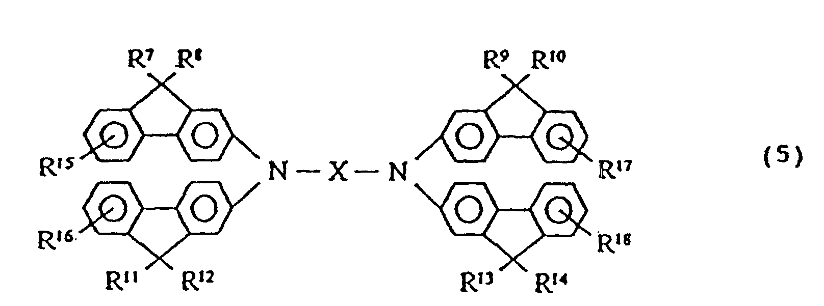
- R 7 , R 8 , R 9 , R 10 , R 11 , R 12 , R 13 , and R 14 are each independently a hydrogen or halogen atom, or a substituted or unsubstituted alkyl, alkoxyl, or aryl group, and examples of such atoms and groups are the same as in R 1 , R 2 , R 3 , and R 4 .
- Each of R 15 , R 16 , R 17 , and R 18 is independently a hydrogen or halogen atom, a nitro or cyano group, or a substituted or unsubstituted alkyl, alkoxyl, aryl, amino or carbonyl group, and examples of such atoms and groups are the same as in R 5 and R 6 .
- An organic compound represented by the formula (1) is synthesized by reaction of an iodine compound with an amine compound.
- the reaction is preferably performed in the presence of a metallic catalyst, for example, a copper catalyst.
- a compound represented by the formula (2) is allowed to react with a compound represented by the formula (3): I-X-I wherein X is a substituted or unsubstituted arylene group, or a substituted or unsubstituted heterocyclic group; wherein Ar and Ar' are each a substituted or unsubstituted fluorenyl group or a substituted or unsubstituted aryl group.
- the organic compound represented by the general formula (1) is thereby prepared: wherein each of at least two groups among Ar 1 , Ar 2 , Ar 3 , and Ar 4 is a substituted or unsubstituted fluorenyl group, and the remainder represents a substituted or unsubstituted aryl group.
- the present invention also includes an electroluminescent device.
- the electroluminescent device in accordance with the present invention comprises a pair of electrodes and an organic layer composed of the organic compound represented by the formula (1) displaced between the electrodes.
- the organic compound is formed between the positive and negative electrodes by a vacuum evaporation or solution coating process.
- the thickness of the organic layer is preferably 2 ⁇ m or less, more preferably 0.5 ⁇ m or less, and most preferably 1 nm to 500 nm.
- a plurality of layers may be provided between the two electrodes.
- at least one layer among these layers is composed of the compound represented by the formula (1).
- the luminescent color of the electroluminescent device can be determined by selecting the compound represented by the formula (1).
- Fig. 1 is a schematic cross-sectional view of an embodiment of the electroluminescent device in accordance with the present invention.
- a positive electrode 2, a luminescent layer 3 and a negative electrode 4 are formed on a substrate 1 in that order.
- the luminescent layer 3 may be composed of a single compound having hole transportability, electron transportability and luminescence, or a mixture of compounds each having one of these properties.
- Fig. 2 is a schematic cross-sectional view of another embodiment of the electroluminescent device in accordance with the present invention.
- a positive electrode 2, a hole transport layer 5, an electron transport layer 6 and a negative electrode 4 are formed on a substrate 1 in that order.
- the hole transport layer 5 and the electron transport layer 6 function as a luminescent, layer 3.
- the hole transport layer 5 may be composed of a luminescent material having hole transportability or a mixture including such a material and a non-luminescent material having hole transportability.
- the luminescent and non-luminescent materials may also have electron transportability.
- the electron transport layer 6 may be composed of a luminescent material having electron transportability or a mixture including such a material and a non-luminescent material having electron transportability.
- the luminescent and non-luminescent materials may also have hole transportability.
- Fig. 3 is a schematic cross-sectional view of a further embodiment of the electroluminescent device in accordance with the present invention.
- a positive electrode 2, a hole transport layer 5, a luminescent layer 3, an electron transport layer 6 and a negative electrode 4 are formed on a substrate 1 in that order.
- carrier transport and luminescence are performed in the individual layers.
- Such a configuration permits a wide variety of combinations of a material having excellent hole transportability, a material having excellent electron transportability and a material having excellent luminescence.
- the configuration permits the use of various compounds emitting light with different wavelengths; hence the hue of the luminescent light can be controlled within a wide range. Trapping effectively holes and electrons (or excimers) in the central luminescent layer will increase the luminescent efficiency.
- Fig. 4 is a schematic cross-sectional view of a still further embodiment of the electroluminescent device in accordance with the present invention.
- a positive electrode 2, a hole injection/transport layer 7, a hole transport layer 5, an electron transport layer 6 and a negative electrode 4 are formed on a substrate 1 in that order.
- the organic compound in accordance with the present invention represented by the formula (1) has excellent luminescence compared to known compounds, and can be used for the electroluminescent devices shown in Figs. 1 to 4.
- the organic compound represented by the formula (1) has hole transportability and/or carrier transportability depending on the types of the substituent groups.
- An organic compound or a combination of different organic compounds may be used in all the configurations shown in Figs. 1 to 4.
- another layer or other layers composed of other materials other than the compound represented by the formula (1) can be provided in addition to at least one organic compound layer.
- the organic compound represented by the formula (1) is used as a constituent in the luminescent layer or a charge transport layer.
- These layers may further include various compounds used in electrophotographic photosensitive members and the like.
- the compounds include hole transport materials, luminescent hole transport materials (for example, compounds shown in Tables 1 to 5), electron transport materials, and luminescent electron transport materials (for example, compounds shown in Tables 6 to 9).
- Table 10 illustrates examples of dopant dyes. The addition of a trace amount of dopant dye in the luminescent layer will significantly increase the luminescent efficiency or will change the luminescent color.
- each layer on the substrate is formed by a vacuum evaporation process or a coating process using a combination of the relevant compound and a suitable binding resin.
- Non-limiting examples of the binding resins include polyvinyl carbazole resins, polycarbonate resins, polyester resins, polyarylate resins, butyral resins, polystyrene resins, polyvinyl acetal resins, diallyl phthalate resins, acrylate resins, methacrylate resins, phenol resins, epoxy resins, silicon resins, polysulfone resins, and urea resins.
- binding resins can be used alone or in combination.
- Materials for the positive electrode have preferably large work functions.
- preferred materials include nickel, gold, platinum, palladium, selenium, rhenium, and iridium, alloys thereof, tin oxide, indium tin oxide (ITO), and copper iodide.
- conductive polymers such as poly(3-methylthiophene), polyphenylene sulfide and polypyrrole, can be used.
- Preferred materials for the negative electrode have small work functions. Examples of such materials include silver, lead, tin, magnesium, aluminum, calcium, manganese, indium and chromium, and alloys thereof.
- At least one of the materials for the positive and negative electrodes has a transmittance of at least 50% at the wavelength range of the light emerging from the electroluminescent device.
- Examples of transparent substrates used in the present invention include glass plates and plastic films.
- the product had a melting point (Tm) of ranging from 309.0 °C to 310.5 °C and a glass transition temperature (Tg) of 186 °C which were determined by a differential scanning calorimeter made by Perkin-Elmer Corporation. An infrared spectrum of the product was taken with a JASCO FT-IR spectrometer. The spectrum is shown in Fig. 5.
- the product had a melting point (Tm) ranging from 267.0 °C to 268.5 °C and a glass transition temperature (Tg) of 120.5 °C which were determined as in Example 1.
- Tm melting point
- Tg glass transition temperature
- An electroluminescent device was prepared to determine the luminance.
- ITO indium tin oxide
- An organic layer with a thickness of 65 nm composed of Compound 13 was formed on the transparent substrate, and an aluminum quinolinol layer with a thickness of 65 nm was formed thereon.
- a direct current of 11 V was applied between the ITO positive electrode and the Mg/Ag negative electrode of the device.
- a current flow of 37 mA/cm 2 and a green luminescence having a luminance of 2,130 cd/m 2 were observed.
- a voltage with a current density of 4.7 mA/cm 2 was applied to the device for 100 hours in a nitrogen stream. The luminance was 180 cd/m 2 at the start and slightly changed to 155 cd/m 2 at the end.
- Electroluminescent devices were prepared and evaluated as in Example 3 using Compound 8, 38, 48, 51 and 52 instead of the Compound 13.
- An electroluminescent device was prepared and evaluated as in Example 3 using the following compound instead of the Compound 13.
- a direct current of 15 V was applied between the ITO positive electrode and the Mg/Ag negative electrode.
- a current flow of 15 mA/cm 2 and a green luminescence having a luminance of 35 cd/m 2 were observed.
- a voltage with a current density of 27 mA/cm 2 was applied to the device for 100 hours in a nitrogen stream. The luminance was 100 cd/m 2 at the start and significantly decreased to 8 cd/m 2 at the end.
- An electroluminescent device having a configuration as shown in Fig. 4 was produced.
- a transparent glass substrate 1 provided with an ITO positive electrode 2 having a thickness of 100 nm deposited by a sputtering process was washed.
- a hole injection/transfer layer 7 with a thickness of 20 nm was formed using Compound 53 on the transparent substrate, and then a hole transport layer 5 of 50 nm was formed thereon using a hole transport compound TPD represented by the following formula.
- An electron transport layer 6 of 65 nm was formed thereon using an electron transport compound (Alq 3 ) represented by the following formula, and then an aluminum negative electrode 4 of 150 nm was formed.
- a direct current of 15 V was applied between the ITO positive electrode and the Al negative electrode.
- a current flow of 230 mA/cm 2 and a green luminescence having a luminance of 23,000 cd/m 2 were observed.
- a voltage with a current density of 4.3 mA/cm 2 was applied to the sample for 100 hours in a nitrogen stream. The luminance was 200 cd/m 2 at the start and slightly decreased to 185 cd/m 2 at the end.
- a transparent glass substrate provided with an ITO layer having a thickness of 100 nm deposited by a sputtering process was washed.
- a hole transfer layer 5 with a thickness of 60 nm was formed using Compound 46 on the transparent substrate, and then a luminescent layer 3 of 10 nm was formed thereon using a fluorescent dye DCM represented by the following formula.
- An electron transport layer 6 of 65 nm was formed thereon using the above-mentioned electron transport compound (Alq 3 ), and then an aluminum negative electrode 4 of 150 nm was formed.
- An electroluminescent device having a configuration as shown in Fig. 3 was thereby formed.
- a direct current of 17 V was applied between the ITO positive electrode and the Al negative electrode.
- a current flow of 150 mA/cm 2 and an orange luminescence having a luminance of 3.170 cd/m 2 were observed.
- a voltage with a current density of 5.1 mA/cm 2 was applied to the sample for 100 hours in a nitrogen stream. The luminance was 100 cd/m 2 at the start and slightly decreased to 85 cd/m 2 at the end.
- a transparent glass substrate provided with an ITO layer having a thickness of 100 nm deposited by a sputtering process was washed.
- 0.10 g of Compound 17 and 0.01 g of an oxadiazole compound (OXD-7) represented by the formula below, and a polycarbonate resin having a weight average molecular weight of 35,000 were dissolved into 25 ml of tetrahydrofuran to prepare a coating solution.
- the coating solution was applied onto the transparent substrate by a dip coating process to form a coating layer with a thickness of 120 nm as a luminescent layer.
- a Mg/In metallic electrode with a thickness of 150 nm was deposited thereon to form a device having the configuration shown in Fig. 1.
- a direct current of 12 V was applied between the ITO positive electrode and the Mg/In negative electrode.
- a current flow of 25 mA/cm 2 and a bluish green luminescence having a luminance of 250 cd/m 2 were observed.
- a voltage with a current density of 10 mA/cm 2 was applied to the sample for 100 hours. The luminance was 130 cd/m 2 at the start and slightly decreased to 95 cd/m 2 at the end.
- a direct current of 15 V was applied between the ITO positive electrode the Mg/Ag negative electrode.
- a current flow of 20 mA/cm 2 and a green luminescence having a luminance of 41 cd/m 2 were observed.
- a voltage with a current density of 15 mA/cm 2 was applied to the sample for 100 hours. The luminance was 30 cd/m 2 at the start and changed to less than 1 cd/m 2 at the end.
Landscapes
- Chemical & Material Sciences (AREA)
- Engineering & Computer Science (AREA)
- Materials Engineering (AREA)
- Physics & Mathematics (AREA)
- Spectroscopy & Molecular Physics (AREA)
- Organic Chemistry (AREA)
- Electroluminescent Light Sources (AREA)
Claims (18)
- Organische Verbindung, dargestellt durch die nachfolgende allgemeine Formel (1):worin X eine substituierte oder unsubstituierte Arylengruppe oder eine substituierte oder unsubstituierte heterozyklische Gruppe ist, wobei jede von mindestens zwei Gruppen aus Ar1, Ar2, Ar3 und Ar4 eine substituierte oder unsubstituierte Fluorenylgruppe ist und das Übrige eine substituierte oder unsubstituierte Arylgruppe darstellt.

- Verbindung nach Anspruch 1, wobei die Arylengruppe eine Phenylen-, Biphenylen-, Terphenylen-, Napthylen-, Fluorenylen-, Pyrenylen- oder Stilben-Gruppe ist.
- Verbindung nach Anspruch 1, wobei die heterozyklische Gruppe aus divalenten Struktureinheiten der Verbindungen ausgewählt ist, die aus Carbazol, Dibenzofuran, Dibenzothiophen, Fluorenon, Oxazol, Oxadiazol, und Thiadiazol bestehen.
- Organische Verbindung gemäß irgendeinem der vorangehenden Ansprüche, wobei jede der Substituenten-Gruppen aus Halogenatomen, Alkylgruppen, Alkoxygruppen, Aralkylgruppen, einer Nitrogruppe, einer Cyanogruppe, Aminogruppen, Arylgruppen und heterozyklischen Gruppen ausgewählt ist.
- Verbindung gemäß irgendeinem der vorangehenden Ansprüche, wobei die Arylgruppe aus Phenylgruppen und polyzyklischen Arylgruppen und heterozyklischen Arylgruppen ausgewählt ist.
- Verbindung nach Anspruch 5, wobei die Arylgruppe einen Substituenten besitzt, der aus Halogenatomen, Alkylgruppen, Alkoxylgruppen, Aralkylgruppen, einer Nitrogruppe, einer Cyanogruppe, Aminogruppen, Arylgruppen und heterozyklischen Gruppen ausgewählt ist.
- Verbindung gemäß irgendeinem der vorangehenden Ansprüche, wobei jede der einen Gruppe von Ar1 und Ar3 und der einen Gruppe von Ar2 und Ar4 eine substituierte oder unsubstituierte Fluorenylgruppe umfasst.
- Verbindung gemäß irgendeinem der Ansprüche 1 bis 6, wobei jede der Ar1- und Ar3- Gruppen eine substituierte oder unsubstituierte Fluorenylgruppe umfasst.
- Verbindung gemäß irgendeinem der Ansprüche 1 bis 6, wobei jede der Ar2 - und Ar4 -Gruppen eine substituierte oder unsubstituierte Fluorenylgruppe umfasst.
- Organische Verbindung gemäß irgendeinem der Ansprüche 1 bis 6, wobei jede der einen Gruppe von Ar1 und Ar3 und beide Gruppen Ar2 und Ar4 eine substituierte oder unsubstituierte Fluorenylgruppe umfasst.
- Verbindung gemäß irgendeinem der Ansprüche 1 bis 6, wobei jede Gruppe von Ar1, Ar2, Ar3 und Ar4 eine substituierte oder unsubstituierte Fluorenylgruppe umfasst.
- Verbindung gemäß irgendeinem der Ansprüche 1 bis 6, wobei jede von einer Gruppe von Ar2 und Ar4 und beide Gruppen Ar1 und Ar3 eine substituierte oder unsubstituierte Fluorenylgruppe umfasst.
- Verbindung gemäß irgendeinem der Ansprüche 1 bis 4, dargestellt durch Formel (4):worin X eine substituierte oder unsubstituierte Arylengruppe oder eine substituierte oder unsubstituierte heterozyklische Gruppe ist; Ar1 und Ar2 jeweils eine substituierte oder unsubstituierte Arylgruppe ist; R1, R2, R3, und R4 jeweils unabhängig voneinander ein Wasserstoff- oder Halogenatom oder eine substituierte oder unsubstituierte Alkyl-, Alkoxyl- oder Aryl-Gruppe ist; und R5 und R6 jeweils unabhängig voneinander ein Wasserstoff- oder Halogenatom, eine Nitro- oder Cyanogruppe oder eine substituierte oder unsubstituierte Alkyl-, Alkoxyl-, Aryl-, Amino- oder Carbonylgruppe ist.

- Verbindung gemäß irgendeinem der Ansprüche 1 bis 4, dargestellt durch die Formel (5):worin X eine substituierte oder unsubstituierte Arylengruppe oder eine substituierte oder unsubstituierte heterozyklische Gruppe ist; R7, R8, R9, R10, R11, R12, R13 und R14 jeweils unabhängig voneinander ein Wasserstoff- oder Halogenatom oder eine substituierte oder unsubstituierte Alkyl-, Alkoxyl- oder Arylgruppe ist; und jede Gruppe von R15, R16, R17, R18 unabhängig voneinander ein Wasserstoff- oder Halogenatom, eine Nitro- oder Cyanogruppe oder eine substituierte oder unsubstituierte Alkyl-, Alkoxyl-, Aryl-, Amino- oder Carbonylgruppe ist.
- Verfahren zum Herstellen irgendeiner der Verbindungen der Ansprüche 1 bis 14, welches das Umsetzen einer Verbindung der Formel (2):worin Ar und Ar' jeweils eine substituierte oder unsubstituierte Fluorenylgruppe oder eine substituierte oder unsubstituierte Arylgruppe ist, umfasst.

- Elektrolumineszenzvorrichtung, umfassend ein Elektrodenpaar und eine zwischen den Elektroden gelagerte Schicht einer organischen Verbindung, wobei die Schicht der organischen Verbindung eine organische Verbindung wie in irgendeinem der Ansprüche 1 bis 14 beansprucht umfasst.
- Vorrichtung gemäß Anspruch 16, wobei die Schicht der organischen Verbindung ferner ein Material zum Transport von Löchern, ein Material zum Transport von Elektronen oder ein Material zum Transport von Lumineszenzlöchern oder Elektronen umfasst.
- Vorrichtung gemäß Anspruch 16 oder 17, wobei die Schicht der organischen Verbindung ferner einen Dotierfarbstoff umfasst.
Applications Claiming Priority (3)
| Application Number | Priority Date | Filing Date | Title |
|---|---|---|---|
| JP14295897 | 1997-05-19 | ||
| JP14295897 | 1997-05-19 | ||
| JP142958/97 | 1997-05-19 |
Publications (3)
| Publication Number | Publication Date |
|---|---|
| EP0879868A2 EP0879868A2 (de) | 1998-11-25 |
| EP0879868A3 EP0879868A3 (de) | 1999-01-07 |
| EP0879868B1 true EP0879868B1 (de) | 2002-04-03 |
Family
ID=15327621
Family Applications (1)
| Application Number | Title | Priority Date | Filing Date |
|---|---|---|---|
| EP98303790A Expired - Lifetime EP0879868B1 (de) | 1997-05-19 | 1998-05-14 | Organisches Material und elektrolumineszente Vorrichtung dasselbe nutzend |
Country Status (3)
| Country | Link |
|---|---|
| US (2) | US6517957B1 (de) |
| EP (1) | EP0879868B1 (de) |
| DE (1) | DE69804529T2 (de) |
Cited By (1)
| Publication number | Priority date | Publication date | Assignee | Title |
|---|---|---|---|---|
| US7241512B2 (en) | 2002-04-19 | 2007-07-10 | 3M Innovative Properties Company | Electroluminescent materials and methods of manufacture and use |
Families Citing this family (160)
| Publication number | Priority date | Publication date | Assignee | Title |
|---|---|---|---|---|
| US6387544B1 (en) * | 1998-04-10 | 2002-05-14 | The Trustees Of Princeton University | OLEDS containing thermally stable glassy organic hole transporting materials |
| DE69914523T2 (de) * | 1998-04-28 | 2005-02-03 | Canon K.K. | Triarylaminverbindungen und lumineszente Vorrichtung |
| US6833200B2 (en) | 1998-04-28 | 2004-12-21 | Canon Kabushiki Kaisha | Luminescent device with a triarylamine compound |
| JP4838969B2 (ja) * | 2000-09-01 | 2011-12-14 | 出光興産株式会社 | 新規スチリル化合物及び有機エレクトロルミネッセンス素子 |
| JP3998903B2 (ja) | 2000-09-05 | 2007-10-31 | 出光興産株式会社 | 新規アリールアミン化合物及び有機エレクトロルミネッセンス素子 |
| JP2002208474A (ja) * | 2001-01-11 | 2002-07-26 | Tohoku Pioneer Corp | 有機elディスプレイ |
| WO2002104080A1 (fr) | 2001-06-15 | 2002-12-27 | Canon Kabushiki Kaisha | Dispositif a electroluminescence organique |
| GB0117377D0 (en) * | 2001-07-17 | 2001-09-05 | Opsys Ltd | "Tertiary diamines containing heterocyclic groups and their use in organic electroluminescent devices" |
| JP3848262B2 (ja) * | 2002-03-27 | 2006-11-22 | キヤノン株式会社 | オリゴフルオレニレン化合物及び有機発光素子 |
| US7282275B2 (en) | 2002-04-19 | 2007-10-16 | 3M Innovative Properties Company | Materials for organic electronic devices |
| US20040062947A1 (en) * | 2002-09-25 | 2004-04-01 | Lamansky Sergey A. | Organic electroluminescent compositions |
| US7094902B2 (en) | 2002-09-25 | 2006-08-22 | 3M Innovative Properties Company | Electroactive polymers |
| JP2004262761A (ja) * | 2003-01-16 | 2004-09-24 | Idemitsu Kosan Co Ltd | 芳香族アミン誘導体及びそれを用いた有機エレクトロルミネッセンス素子 |
| EP1604974A4 (de) * | 2003-03-20 | 2007-11-14 | Idemitsu Kosan Co | Aromatische aminderivate und unter verwendung dieser hergestelltes organisches elektrolumineszentes element |
| US7271406B2 (en) | 2003-04-15 | 2007-09-18 | 3M Innovative Properties Company | Electron transport agents for organic electronic devices |
| US7192657B2 (en) | 2003-04-15 | 2007-03-20 | 3M Innovative Properties Company | Ethynyl containing electron transport dyes and compositions |
| JP4464070B2 (ja) | 2003-05-15 | 2010-05-19 | 出光興産株式会社 | アリールアミン化合物及びそれを用いた有機エレクトロルミネッセンス素子 |
| US7651746B2 (en) * | 2003-11-14 | 2010-01-26 | Sumitomo Chemical Company, Limited | Halogenated bisdiarylaminopolycyclic aromatic compounds and polymers thereof |
| WO2005073337A1 (en) * | 2004-01-30 | 2005-08-11 | Sk Corporation | Organic electroluminescent polymer having 9,9-di(fluorenyl)-2,7-fluorenyl unit and organic electroluminescent device manufactured using the same |
| US7960587B2 (en) * | 2004-02-19 | 2011-06-14 | E.I. Du Pont De Nemours And Company | Compositions comprising novel compounds and electronic devices made with such compositions |
| US7365230B2 (en) * | 2004-02-20 | 2008-04-29 | E.I. Du Pont De Nemours And Company | Cross-linkable polymers and electronic devices made with such polymers |
| CN101002506B (zh) | 2004-03-31 | 2014-06-25 | E.I.内穆尔杜邦公司 | 用作电荷传输物质的三芳胺化合物 |
| US8188315B2 (en) * | 2004-04-02 | 2012-05-29 | Samsung Mobile Display Co., Ltd. | Organic light emitting device and flat panel display device comprising the same |
| KR100573137B1 (ko) * | 2004-04-02 | 2006-04-24 | 삼성에스디아이 주식회사 | 플루오렌계 화합물 및 이를 이용한 유기 전계 발광 소자 |
| KR100787425B1 (ko) * | 2004-11-29 | 2007-12-26 | 삼성에스디아이 주식회사 | 페닐카바졸계 화합물 및 이를 이용한 유기 전계 발광 소자 |
| EP1762562A4 (de) * | 2004-06-28 | 2007-10-31 | Idemitsu Kosan Co | Aromatisches aminderivat und organisches elektrolumineszentes element, bei dem dieses verwendet wird |
| US8021765B2 (en) * | 2004-11-29 | 2011-09-20 | Samsung Mobile Display Co., Ltd. | Phenylcarbazole-based compound and organic electroluminescent device employing the same |
| US8950328B1 (en) | 2004-12-29 | 2015-02-10 | E I Du Pont De Nemours And Company | Methods of fabricating organic electronic devices |
| KR101239462B1 (ko) * | 2005-01-05 | 2013-03-06 | 이데미쓰 고산 가부시키가이샤 | 방향족 아민 유도체 및 이를 이용한 유기 전기발광 소자 |
| KR101425423B1 (ko) | 2005-05-30 | 2014-08-01 | 시바 홀딩 인크 | 전계발광 장치 |
| JP4848152B2 (ja) * | 2005-08-08 | 2011-12-28 | 出光興産株式会社 | 芳香族アミン誘導体及びそれを用いた有機エレクトロルミネッセンス素子 |
| US7656575B2 (en) * | 2005-08-31 | 2010-02-02 | Padilla Patrick T | Printable pixel structure with carbon fiber emitters |
| JP5268247B2 (ja) * | 2005-12-20 | 2013-08-21 | キヤノン株式会社 | 4−アミノフルオレン化合物及び有機発光素子 |
| JP4653061B2 (ja) * | 2005-12-20 | 2011-03-16 | キヤノン株式会社 | アミン化合物および有機発光素子および青色有機発光素子 |
| JP2007186461A (ja) * | 2006-01-13 | 2007-07-26 | Idemitsu Kosan Co Ltd | 芳香族アミン誘導体及びそれを用いた有機エレクトロルミネッセンス素子 |
| CN101395106B (zh) * | 2006-04-20 | 2013-02-06 | 佳能株式会社 | 二苯并蒽化合物和具有该化合物的有机发光器件 |
| US8623522B2 (en) | 2006-04-26 | 2014-01-07 | Idemitsu Kosan Co., Ltd. | Aromatic amine derivative and electroluminescence device using the same |
| KR101453109B1 (ko) * | 2006-04-26 | 2014-10-27 | 이데미쓰 고산 가부시키가이샤 | 방향족 아민 유도체 및 그들을 이용한 유기 전기 발광 소자 |
| JP5153127B2 (ja) * | 2006-11-28 | 2013-02-27 | キヤノン株式会社 | アミン化合物及び有機発光素子 |
| JP5121848B2 (ja) | 2006-12-08 | 2013-01-16 | エージェンシー フォー サイエンス, テクノロジー アンド リサーチ | アリールアミン化合物および電子素子 |
| DE102006059215A1 (de) * | 2006-12-13 | 2008-07-10 | Sensient Imaging Technologies Gmbh | Arylaminsubstituierte Divinylfluorene und ihre Nutzung für elektrofotografische Anwendungen und für OLEDS (Organic Light Emitting Devices) |
| JP2008162911A (ja) * | 2006-12-27 | 2008-07-17 | Canon Inc | ジアザフルオレン化合物 |
| US8626643B2 (en) * | 2007-05-03 | 2014-01-07 | Orion Energy Systems, Inc. | System and method for a utility financial model |
| EP2213693A4 (de) * | 2007-11-20 | 2011-11-09 | Idemitsu Kosan Co | Polymerverbindung und organisches elektrolumineszenzelement damit |
| KR100974139B1 (ko) * | 2007-12-24 | 2010-08-04 | 주식회사 두산 | 아릴 아민 유도체 및 이를 이용한 유기 전계 발광 소자 |
| KR20100097182A (ko) * | 2007-12-28 | 2010-09-02 | 이데미쓰 고산 가부시키가이샤 | 방향족 다이아민 유도체 및 그것을 이용한 유기 전기발광 소자 |
| KR101121703B1 (ko) | 2007-12-28 | 2012-03-13 | 이데미쓰 고산 가부시키가이샤 | 방향족 아민 유도체 및 그것을 이용한 유기 전기발광 소자 |
| KR100964223B1 (ko) * | 2008-02-11 | 2010-06-17 | 삼성모바일디스플레이주식회사 | 유기 발광 소자 및 이를 구비한 평판 표시 장치 |
| KR101042954B1 (ko) * | 2008-07-30 | 2011-06-20 | 삼성모바일디스플레이주식회사 | 아민계 화합물, 이를 포함한 유기 발광 소자 및 이러한유기 발광 소자를 구비한 평판 표시 장치 |
| KR101050459B1 (ko) * | 2008-09-03 | 2011-07-20 | 삼성모바일디스플레이주식회사 | 플루오렌 화합물 및 이를 이용한 유기 전계 발광 장치 |
| EP2423206B1 (de) | 2009-04-24 | 2014-01-08 | Idemitsu Kosan Co., Ltd. | Aromatische aminderivate und deren verwendung in organischen elektrolumineszenzelementen |
| TWI471309B (zh) | 2009-06-03 | 2015-02-01 | Fujifilm Corp | 光電變換元件及其製造方法、光感測器與攝像元件及它們的驅動方法 |
| CN102482215B (zh) | 2009-08-19 | 2015-04-15 | 出光兴产株式会社 | 芳胺衍生物及使用该芳胺衍生物的有机电致发光元件 |
| JP2013508380A (ja) | 2009-10-19 | 2013-03-07 | イー・アイ・デュポン・ドウ・ヌムール・アンド・カンパニー | 電子用途用のトリアリールアミン化合物 |
| WO2011049904A2 (en) | 2009-10-19 | 2011-04-28 | E. I. Du Pont De Nemours And Company | Triarylamine compounds for electronic applications |
| US8642190B2 (en) | 2009-10-22 | 2014-02-04 | Semiconductor Energy Laboratory Co., Ltd. | Fluorene derivative, light-emitting element, light-emitting device, electronic device, and lighting device |
| US20120319091A1 (en) * | 2010-01-21 | 2012-12-20 | Idemitsu Kosan Co., Ltd. | Aromatic amine derivative, and organic electroluminescent element comprising same |
| GB201200619D0 (en) | 2012-01-16 | 2012-02-29 | Cambridge Display Tech Ltd | Polymer |
| JP6158542B2 (ja) | 2012-04-13 | 2017-07-05 | 株式会社半導体エネルギー研究所 | 発光素子、発光装置、電子機器、および照明装置 |
| JP6382193B2 (ja) * | 2012-07-23 | 2018-08-29 | メルク パテント ゲーエムベーハー | 化合物および有機エレクトロルミッセンス素子 |
| TWI587557B (zh) | 2012-08-03 | 2017-06-11 | 半導體能源研究所股份有限公司 | 發光元件、發光裝置、顯示裝置、電子裝置及照明設備 |
| US10043982B2 (en) | 2013-04-26 | 2018-08-07 | Semiconductor Energy Laboratory Co., Ltd. | Light-emitting element, light-emitting device, display device, electronic device, and lighting device |
| US20160131985A1 (en) * | 2014-11-11 | 2016-05-12 | Canon Kabushiki Kaisha | Electrophotographic photosensitive member, process cartridge, and electrophotographic apparatus |
| EP3247765B1 (de) * | 2015-01-20 | 2018-11-07 | cynora GmbH | Azole zur verwendung in optoelektronischen bauelementen |
| US9929361B2 (en) | 2015-02-16 | 2018-03-27 | Universal Display Corporation | Organic electroluminescent materials and devices |
| US11056657B2 (en) | 2015-02-27 | 2021-07-06 | University Display Corporation | Organic electroluminescent materials and devices |
| US9859510B2 (en) | 2015-05-15 | 2018-01-02 | Universal Display Corporation | Organic electroluminescent materials and devices |
| US10418568B2 (en) | 2015-06-01 | 2019-09-17 | Universal Display Corporation | Organic electroluminescent materials and devices |
| US11127905B2 (en) | 2015-07-29 | 2021-09-21 | Universal Display Corporation | Organic electroluminescent materials and devices |
| WO2017038613A1 (ja) | 2015-08-28 | 2017-03-09 | 住友化学株式会社 | 組成物及びそれを用いた発光素子 |
| US10361381B2 (en) | 2015-09-03 | 2019-07-23 | Universal Display Corporation | Organic electroluminescent materials and devices |
| KR20170075122A (ko) | 2015-12-22 | 2017-07-03 | 삼성디스플레이 주식회사 | 유기 발광 소자 |
| KR102579752B1 (ko) | 2015-12-22 | 2023-09-19 | 삼성디스플레이 주식회사 | 유기 발광 소자 |
| KR102579753B1 (ko) * | 2015-12-22 | 2023-09-19 | 삼성디스플레이 주식회사 | 유기 발광 소자 |
| KR20170075114A (ko) | 2015-12-22 | 2017-07-03 | 삼성디스플레이 주식회사 | 유기 발광 소자 |
| US20170229663A1 (en) | 2016-02-09 | 2017-08-10 | Universal Display Corporation | Organic electroluminescent materials and devices |
| US10236456B2 (en) | 2016-04-11 | 2019-03-19 | Universal Display Corporation | Organic electroluminescent materials and devices |
| KR102018682B1 (ko) * | 2016-05-26 | 2019-09-04 | 덕산네오룩스 주식회사 | 유기전기소자용 화합물, 이를 이용한 유기전기소자 및 그 전자 장치 |
| US11482683B2 (en) | 2016-06-20 | 2022-10-25 | Universal Display Corporation | Organic electroluminescent materials and devices |
| US10672997B2 (en) | 2016-06-20 | 2020-06-02 | Universal Display Corporation | Organic electroluminescent materials and devices |
| US10862054B2 (en) | 2016-06-20 | 2020-12-08 | Universal Display Corporation | Organic electroluminescent materials and devices |
| US10608186B2 (en) | 2016-09-14 | 2020-03-31 | Universal Display Corporation | Organic electroluminescent materials and devices |
| US10680187B2 (en) | 2016-09-23 | 2020-06-09 | Universal Display Corporation | Organic electroluminescent materials and devices |
| CN106478566A (zh) * | 2016-09-27 | 2017-03-08 | 上海道亦化工科技有限公司 | 基于二苯并呋喃的有机电致发光化合物及其有机电致发光器件 |
| US11196010B2 (en) | 2016-10-03 | 2021-12-07 | Universal Display Corporation | Organic electroluminescent materials and devices |
| US11011709B2 (en) | 2016-10-07 | 2021-05-18 | Universal Display Corporation | Organic electroluminescent materials and devices |
| US12317745B2 (en) | 2016-11-09 | 2025-05-27 | Universal Display Corporation | Organic electroluminescent materials and devices |
| US10680188B2 (en) | 2016-11-11 | 2020-06-09 | Universal Display Corporation | Organic electroluminescent materials and devices |
| CN106674026B (zh) * | 2016-12-28 | 2019-06-21 | 上海天马有机发光显示技术有限公司 | 一种空穴传输材料、包含其的oled显示面板和电子设备 |
| US11780865B2 (en) | 2017-01-09 | 2023-10-10 | Universal Display Corporation | Organic electroluminescent materials and devices |
| US10844085B2 (en) | 2017-03-29 | 2020-11-24 | Universal Display Corporation | Organic electroluminescent materials and devices |
| US10944060B2 (en) | 2017-05-11 | 2021-03-09 | Universal Display Corporation | Organic electroluminescent materials and devices |
| US12098157B2 (en) | 2017-06-23 | 2024-09-24 | Universal Display Corporation | Organic electroluminescent materials and devices |
| US11228010B2 (en) | 2017-07-26 | 2022-01-18 | Universal Display Corporation | Organic electroluminescent materials and devices |
| US11744142B2 (en) | 2017-08-10 | 2023-08-29 | Universal Display Corporation | Organic electroluminescent materials and devices |
| KR20190038254A (ko) * | 2017-09-29 | 2019-04-08 | 덕산네오룩스 주식회사 | 유기전기 소자용 화합물, 이를 이용한 유기전기소자 및 그 전자 장치 |
| KR102477890B1 (ko) | 2017-11-08 | 2022-12-15 | 덕산네오룩스 주식회사 | 유기전기소자용 화합물을 이용한 유기전기소자 및 그 전자 장치 |
| US12180230B2 (en) | 2017-11-28 | 2024-12-31 | University Of Southern California | Carbene compounds and organic electroluminescent devices |
| EP3492480B1 (de) | 2017-11-29 | 2021-10-20 | Universal Display Corporation | Organische elektrolumineszente materialien und vorrichtungen |
| US11937503B2 (en) | 2017-11-30 | 2024-03-19 | Universal Display Corporation | Organic electroluminescent materials and devices |
| US11542289B2 (en) | 2018-01-26 | 2023-01-03 | Universal Display Corporation | Organic electroluminescent materials and devices |
| US11165028B2 (en) | 2018-03-12 | 2021-11-02 | Universal Display Corporation | Organic electroluminescent materials and devices |
| KR20190140549A (ko) | 2018-06-11 | 2019-12-20 | 삼성디스플레이 주식회사 | 아민 화합물 및 이를 포함한 유기 발광 소자 |
| WO2020017552A1 (ja) * | 2018-07-17 | 2020-01-23 | 保土谷化学工業株式会社 | 有機エレクトロルミネッセンス素子 |
| KR102757332B1 (ko) | 2018-07-27 | 2025-01-21 | 삼성디스플레이 주식회사 | 아민 화합물 및 이를 포함한 유기 발광 소자 |
| US12453279B2 (en) | 2018-08-22 | 2025-10-21 | Universal Display Corporation | Organic electroluminescent materials and devices |
| KR102696821B1 (ko) * | 2018-11-06 | 2024-08-21 | 삼성디스플레이 주식회사 | 아민계 화합물 및 이를 포함한 유기 발광 소자 |
| US11737349B2 (en) | 2018-12-12 | 2023-08-22 | Universal Display Corporation | Organic electroluminescent materials and devices |
| CN109651174B (zh) * | 2019-01-23 | 2022-12-06 | 苏州久显新材料有限公司 | 有机电致发光化合物、发光材料及有机电致发光器件 |
| US11780829B2 (en) | 2019-01-30 | 2023-10-10 | The University Of Southern California | Organic electroluminescent materials and devices |
| US12477890B2 (en) | 2019-02-01 | 2025-11-18 | Universal Display Corporation | Organic electroluminescent materials and devices |
| JP2020158491A (ja) | 2019-03-26 | 2020-10-01 | ユニバーサル ディスプレイ コーポレイション | 有機エレクトロルミネセンス材料及びデバイス |
| CN110256358B (zh) | 2019-07-12 | 2020-03-17 | 长春海谱润斯科技有限公司 | 一种胺类衍生物及其有机电致发光器件 |
| US12281128B2 (en) | 2019-07-30 | 2025-04-22 | Universal Display Corporation | Organic electroluminescent materials and devices |
| US12139501B2 (en) | 2019-08-16 | 2024-11-12 | Universal Display Corporation | Organic electroluminescent materials and devices |
| US20210135130A1 (en) | 2019-11-04 | 2021-05-06 | Universal Display Corporation | Organic electroluminescent materials and devices |
| US12538698B2 (en) | 2020-01-06 | 2026-01-27 | Universal Display Corporation | Organic electroluminescent materials and devices |
| KR102326512B1 (ko) * | 2020-01-14 | 2021-11-16 | 덕산네오룩스 주식회사 | 유기전기소자용 화합물, 이를 이용한 유기전기소자 및 그 전자 장치 |
| US12426495B2 (en) | 2020-01-28 | 2025-09-23 | Universal Display Corporation | Organic electroluminescent materials and devices |
| EP3937268B1 (de) | 2020-07-10 | 2025-05-07 | Universal Display Corporation | Plasmonische oleds und vertikale dipolstrahler |
| CN114181167B (zh) * | 2020-09-14 | 2025-09-26 | 东进世美肯株式会社 | 新型覆盖层用化合物以及包含所述覆盖层用化合物的有机发光元件 |
| US12187748B2 (en) | 2020-11-02 | 2025-01-07 | Universal Display Corporation | Organic electroluminescent materials and devices |
| US20220158096A1 (en) | 2020-11-16 | 2022-05-19 | Universal Display Corporation | Organic electroluminescent materials and devices |
| US12325717B2 (en) | 2020-11-24 | 2025-06-10 | Universal Display Corporation | Organic electroluminescent materials and devices |
| US20220165967A1 (en) | 2020-11-24 | 2022-05-26 | Universal Display Corporation | Organic electroluminescent materials and devices |
| US12575316B2 (en) | 2021-02-03 | 2026-03-10 | Universal Display Corporation | Organic electroluminescent materials and devices |
| EP4060758A3 (de) | 2021-02-26 | 2023-03-29 | Universal Display Corporation | Organische elektrolumineszente materialien und vorrichtungen |
| EP4059915B1 (de) | 2021-02-26 | 2025-12-24 | Universal Display Corporation | Organische elektrolumineszente materialien und vorrichtungen |
| US12624055B2 (en) | 2021-03-01 | 2026-05-12 | Universal Display Corporation | Organic electroluminescent materials and devices |
| US12606582B2 (en) | 2021-03-05 | 2026-04-21 | Universal Display Corporation | Organic electroluminescent materials and devices |
| US12428599B2 (en) | 2021-03-09 | 2025-09-30 | Universal Display Corporation | Organic electroluminescent materials and devices |
| US20220298190A1 (en) | 2021-03-12 | 2022-09-22 | Universal Display Corporation | Organic electroluminescent materials and devices |
| US12421262B2 (en) | 2021-03-15 | 2025-09-23 | Universal Display Corporation | Organic electroluminescent materials and devices |
| US20220340607A1 (en) | 2021-04-05 | 2022-10-27 | Universal Display Corporation | Organic electroluminescent materials and devices |
| US12480042B2 (en) | 2021-04-09 | 2025-11-25 | Universal Display Corporation | Organic electroluminescent materials and devices |
| EP4075531A1 (de) | 2021-04-13 | 2022-10-19 | Universal Display Corporation | Plasmonische oleds und vertikale dipolstrahler |
| US20220352478A1 (en) | 2021-04-14 | 2022-11-03 | Universal Display Corporation | Organic eletroluminescent materials and devices |
| US20230006149A1 (en) | 2021-04-23 | 2023-01-05 | Universal Display Corporation | Organic electroluminescent materials and devices |
| US20220407020A1 (en) | 2021-04-23 | 2022-12-22 | Universal Display Corporation | Organic electroluminescent materials and devices |
| US20230133787A1 (en) | 2021-06-08 | 2023-05-04 | University Of Southern California | Molecular Alignment of Homoleptic Iridium Phosphors |
| US12550611B2 (en) | 2021-08-03 | 2026-02-10 | Universal Display Corporation | Organic electroluminescent materials and devices |
| EP4151699A1 (de) | 2021-09-17 | 2023-03-22 | Universal Display Corporation | Organische elektrolumineszente materialien und vorrichtungen |
| US12473318B2 (en) | 2021-10-08 | 2025-11-18 | Universal Display Corporation | Organic electroluminescent materials and devices |
| US12509628B2 (en) | 2021-12-16 | 2025-12-30 | Universal Display Corporation | Organic electroluminescent materials and devices |
| EP4231804A3 (de) | 2022-02-16 | 2023-09-20 | Universal Display Corporation | Organische elektrolumineszente materialien und vorrichtungen |
| US20230292592A1 (en) | 2022-03-09 | 2023-09-14 | Universal Display Corporation | Organic electroluminescent materials and devices |
| US20230337516A1 (en) | 2022-04-18 | 2023-10-19 | Universal Display Corporation | Organic electroluminescent materials and devices |
| US20230389421A1 (en) | 2022-05-24 | 2023-11-30 | Universal Display Corporation | Organic electroluminescent materials and devices |
| EP4293001A1 (de) | 2022-06-08 | 2023-12-20 | Universal Display Corporation | Organische elektrolumineszente materialien und vorrichtungen |
| WO2023247416A1 (en) | 2022-06-21 | 2023-12-28 | Dottikon Es Holding Ag | Tetraarylbenzidine type compounds and their use in organic electronics |
| US20240016051A1 (en) | 2022-06-28 | 2024-01-11 | Universal Display Corporation | Organic electroluminescent materials and devices |
| US20240107880A1 (en) | 2022-08-17 | 2024-03-28 | Universal Display Corporation | Organic electroluminescent materials and devices |
| US20240188419A1 (en) | 2022-10-27 | 2024-06-06 | Universal Display Corporation | Organic electroluminescent materials and devices |
| US20240180025A1 (en) | 2022-10-27 | 2024-05-30 | Universal Display Corporation | Organic electroluminescent materials and devices |
| US20240188319A1 (en) | 2022-10-27 | 2024-06-06 | Universal Display Corporation | Organic electroluminescent materials and devices |
| US20240196730A1 (en) | 2022-10-27 | 2024-06-13 | Universal Display Corporation | Organic electroluminescent materials and devices |
| US20240188316A1 (en) | 2022-10-27 | 2024-06-06 | Universal Display Corporation | Organic electroluminescent materials and devices |
| US20240247017A1 (en) | 2022-12-14 | 2024-07-25 | Universal Display Corporation | Organic electroluminescent materials and devices |
| US20250204238A1 (en) | 2023-12-15 | 2025-06-19 | Universal Display Corporation | Organic electroluminscent materials and devices |
| US20250204239A1 (en) | 2023-12-15 | 2025-06-19 | Universal Display Corporation | Organic electroluminescent materials and devices |
Citations (2)
| Publication number | Priority date | Publication date | Assignee | Title |
|---|---|---|---|---|
| EP0880304A2 (de) * | 1997-05-19 | 1998-11-25 | Canon Kabushiki Kaisha | Lumineszente Vorrichtung |
| EP0934992A1 (de) * | 1997-03-17 | 1999-08-11 | Toyo Ink Manufacturing Co., Ltd. | Leuchtemittierender Stoff für organische Elektrolumineszensvorrichtung und organische Elektrolumineszensvorrichtung |
Family Cites Families (17)
| Publication number | Priority date | Publication date | Assignee | Title |
|---|---|---|---|---|
| US3172862A (en) | 1960-09-29 | 1965-03-09 | Dow Chemical Co | Organic electroluminescent phosphors |
| US3173050A (en) | 1962-09-19 | 1965-03-09 | Dow Chemical Co | Electroluminescent cell |
| US3710167A (en) | 1970-07-02 | 1973-01-09 | Rca Corp | Organic electroluminescent cells having a tunnel injection cathode |
| US4356429A (en) | 1980-07-17 | 1982-10-26 | Eastman Kodak Company | Organic electroluminescent cell |
| US4539507A (en) | 1983-03-25 | 1985-09-03 | Eastman Kodak Company | Organic electroluminescent devices having improved power conversion efficiencies |
| JPS6219875A (ja) * | 1985-07-18 | 1987-01-28 | Canon Inc | 電子写真感光体 |
| JPS6219876A (ja) * | 1985-07-18 | 1987-01-28 | Canon Inc | 電子写真感光体 |
| US4720432A (en) | 1987-02-11 | 1988-01-19 | Eastman Kodak Company | Electroluminescent device with organic luminescent medium |
| JP2814435B2 (ja) | 1987-03-02 | 1998-10-22 | イーストマン・コダック・カンパニー | 改良薄膜発光帯をもつ電場発光デバイス |
| US4853308A (en) * | 1987-11-09 | 1989-08-01 | Xerox Corporation | Photoresponsive imaging members with fluorene hole transporting layers |
| US5118986A (en) | 1989-06-30 | 1992-06-02 | Ricoh Company, Ltd. | Electroluminescent device |
| JPH03163188A (ja) | 1989-08-18 | 1991-07-15 | Ricoh Co Ltd | 電界発光素子 |
| JP3065130B2 (ja) | 1991-07-22 | 2000-07-12 | 三井化学株式会社 | 有機電界発光素子 |
| US5415962A (en) * | 1992-04-23 | 1995-05-16 | Canon Kabushiki Kaisha | Electrophotographic photosensitive member, electrophotographic apparatus using same and device unit using same |
| JP3269300B2 (ja) * | 1994-12-22 | 2002-03-25 | 東洋インキ製造株式会社 | 正孔輸送材料およびその用途 |
| EP0765106B1 (de) * | 1995-09-25 | 2002-11-27 | Toyo Ink Manufacturing Co., Ltd. | Leuchtemittierender Stoff für organische Elektrolumineszensvorrichtung, und organische Elektrolumineszensvorrichtung mit diesem leuchtemittierendem dafür geeignetem Stoff |
| JP3856550B2 (ja) * | 1997-12-05 | 2006-12-13 | 三井化学株式会社 | 有機電界発光素子 |
-
1998
- 1998-05-14 EP EP98303790A patent/EP0879868B1/de not_active Expired - Lifetime
- 1998-05-14 DE DE69804529T patent/DE69804529T2/de not_active Expired - Lifetime
- 1998-05-14 US US09/078,570 patent/US6517957B1/en not_active Expired - Lifetime
-
2002
- 2002-10-09 US US10/266,602 patent/US6858325B2/en not_active Expired - Lifetime
Patent Citations (2)
| Publication number | Priority date | Publication date | Assignee | Title |
|---|---|---|---|---|
| EP0934992A1 (de) * | 1997-03-17 | 1999-08-11 | Toyo Ink Manufacturing Co., Ltd. | Leuchtemittierender Stoff für organische Elektrolumineszensvorrichtung und organische Elektrolumineszensvorrichtung |
| EP0880304A2 (de) * | 1997-05-19 | 1998-11-25 | Canon Kabushiki Kaisha | Lumineszente Vorrichtung |
Cited By (2)
| Publication number | Priority date | Publication date | Assignee | Title |
|---|---|---|---|---|
| US7241512B2 (en) | 2002-04-19 | 2007-07-10 | 3M Innovative Properties Company | Electroluminescent materials and methods of manufacture and use |
| US7442421B2 (en) | 2002-04-19 | 2008-10-28 | 3M Innovative Properties Company | Electroluminescent materials and methods of manufacture and use |
Also Published As
| Publication number | Publication date |
|---|---|
| US6858325B2 (en) | 2005-02-22 |
| DE69804529D1 (de) | 2002-05-08 |
| DE69804529T2 (de) | 2002-10-02 |
| EP0879868A2 (de) | 1998-11-25 |
| EP0879868A3 (de) | 1999-01-07 |
| US20030157364A1 (en) | 2003-08-21 |
| US6517957B1 (en) | 2003-02-11 |
Similar Documents
| Publication | Publication Date | Title |
|---|---|---|
| US6517957B1 (en) | Organic compound and electroluminescent device using the same | |
| JP3508984B2 (ja) | 有機化合物及び該有機化合物を用いた発光素子 | |
| JP3816969B2 (ja) | 有機el素子 | |
| EP0611148B1 (de) | Trisarylaminobenzolderivate, Verbindungen für ein organisches elektrolumineszierendes Element und organisches elektrolumineszierendes Element | |
| EP0666298A2 (de) | Organisches elektrolumineszentes Element und darin gebrauchte Verbindung | |
| US6761981B2 (en) | Cyclic tertiary amine compound and organic electroluminescent device containing the compound | |
| KR20020062940A (ko) | 신규 아릴아민 화합물 및 유기 전기발광 소자 | |
| JP3965800B2 (ja) | トリアリールアミン誘導体を用いた有機電界発光素子 | |
| JP2003146951A (ja) | アントラセン系化合物、その製造方法および有機電界発光素子 | |
| WO2004101491A1 (ja) | アリールアミン化合物及びそれを用いた有機エレクトロルミネッセンス素子 | |
| JPH10265773A (ja) | 有機エレクトロルミネッセンス素子用正孔注入材料およびそれを使用した有機エレクトロルミネッセンス素子 | |
| JP2000086595A (ja) | トリフェニルアミン誘導体とそれを用いた有機エレクトロルミネッセンス素子 | |
| EP0953624B1 (de) | Triarylaminverbindungen und lumineszente Vorrichtung | |
| JP4545243B2 (ja) | ジアミノナフタレン誘導体、及びそれを用いた有機電界発光素子 | |
| US6534198B1 (en) | Silicon compound, method for making the same, and electroluminescent device using the same | |
| US6833200B2 (en) | Luminescent device with a triarylamine compound | |
| JP2982699B2 (ja) | 多層型有機エレクトロルミネッセンス素子の電子注入層形成用材料 | |
| KR20010031273A (ko) | 아민 유도체 및 이를 사용한 유기 전계발광 소자 | |
| JP2000016973A (ja) | 新規なトリアリ―ルアミン化合物及び該化合物を用いた発光素子 | |
| JP3642606B2 (ja) | 有機el素子 | |
| JP4069505B2 (ja) | トリナフチルベンゼン誘導体、及びそれを用いた有機電界発光素子 | |
| JP3726316B2 (ja) | 電界発光素子 | |
| JP3858278B2 (ja) | 電界発光素子 | |
| KR100505785B1 (ko) | 신규한 트리아릴실릴에티닐기를 갖는 유기실란계 화합물,이를 이용한 유기 el 소자 | |
| JPH10321370A (ja) | 電界発光素子 |
Legal Events
| Date | Code | Title | Description |
|---|---|---|---|
| PUAI | Public reference made under article 153(3) epc to a published international application that has entered the european phase |
Free format text: ORIGINAL CODE: 0009012 |
|
| PUAL | Search report despatched |
Free format text: ORIGINAL CODE: 0009013 |
|
| AK | Designated contracting states |
Kind code of ref document: A2 Designated state(s): DE FR GB NL |
|
| AX | Request for extension of the european patent |
Free format text: AL;LT;LV;MK;RO;SI |
|
| AK | Designated contracting states |
Kind code of ref document: A3 Designated state(s): AT BE CH CY DE DK ES FI FR GB GR IE IT LI LU MC NL PT SE |
|
| AX | Request for extension of the european patent |
Free format text: AL;LT;LV;MK;RO;SI |
|
| 17P | Request for examination filed |
Effective date: 19990519 |
|
| AKX | Designation fees paid |
Free format text: DE FR GB NL |
|
| 17Q | First examination report despatched |
Effective date: 20000721 |
|
| GRAG | Despatch of communication of intention to grant |
Free format text: ORIGINAL CODE: EPIDOS AGRA |
|
| GRAG | Despatch of communication of intention to grant |
Free format text: ORIGINAL CODE: EPIDOS AGRA |
|
| GRAH | Despatch of communication of intention to grant a patent |
Free format text: ORIGINAL CODE: EPIDOS IGRA |
|
| RIN1 | Information on inventor provided before grant (corrected) |
Inventor name: URAKAWA, SHINICHI Inventor name: MASHIMO, SEIJI Inventor name: UENO, KAZUNORI Inventor name: HASHIMOTO, YUICHI Inventor name: TOSHIDA, YOMISHI Inventor name: SENOO, AKIHIRO |
|
| REG | Reference to a national code |
Ref country code: GB Ref legal event code: IF02 |
|
| GRAH | Despatch of communication of intention to grant a patent |
Free format text: ORIGINAL CODE: EPIDOS IGRA |
|
| GRAA | (expected) grant |
Free format text: ORIGINAL CODE: 0009210 |
|
| AK | Designated contracting states |
Kind code of ref document: B1 Designated state(s): DE FR GB NL |
|
| REF | Corresponds to: |
Ref document number: 69804529 Country of ref document: DE Date of ref document: 20020508 |
|
| ET | Fr: translation filed | ||
| RIN2 | Information on inventor provided after grant (corrected) |
Free format text: SENOO, AKIHIRO * TOSHIDA, YOMISHI * UENO, KAZUNORI * MASHIMO, SEIJI |
|
| PLBE | No opposition filed within time limit |
Free format text: ORIGINAL CODE: 0009261 |
|
| STAA | Information on the status of an ep patent application or granted ep patent |
Free format text: STATUS: NO OPPOSITION FILED WITHIN TIME LIMIT |
|
| 26N | No opposition filed |
Effective date: 20030106 |
|
| PGFP | Annual fee paid to national office [announced via postgrant information from national office to epo] |
Ref country code: NL Payment date: 20100517 Year of fee payment: 13 |
|
| REG | Reference to a national code |
Ref country code: NL Ref legal event code: V1 Effective date: 20111201 |
|
| PG25 | Lapsed in a contracting state [announced via postgrant information from national office to epo] |
Ref country code: NL Free format text: LAPSE BECAUSE OF NON-PAYMENT OF DUE FEES Effective date: 20111201 |
|
| REG | Reference to a national code |
Ref country code: FR Ref legal event code: PLFP Year of fee payment: 19 |
|
| PGFP | Annual fee paid to national office [announced via postgrant information from national office to epo] |
Ref country code: GB Payment date: 20160525 Year of fee payment: 19 Ref country code: DE Payment date: 20160531 Year of fee payment: 19 |
|
| PGFP | Annual fee paid to national office [announced via postgrant information from national office to epo] |
Ref country code: FR Payment date: 20160526 Year of fee payment: 19 |
|
| REG | Reference to a national code |
Ref country code: DE Ref legal event code: R119 Ref document number: 69804529 Country of ref document: DE |
|
| GBPC | Gb: european patent ceased through non-payment of renewal fee |
Effective date: 20170514 |
|
| REG | Reference to a national code |
Ref country code: FR Ref legal event code: ST Effective date: 20180131 |
|
| PG25 | Lapsed in a contracting state [announced via postgrant information from national office to epo] |
Ref country code: DE Free format text: LAPSE BECAUSE OF NON-PAYMENT OF DUE FEES Effective date: 20171201 Ref country code: GB Free format text: LAPSE BECAUSE OF NON-PAYMENT OF DUE FEES Effective date: 20170514 |
|
| PG25 | Lapsed in a contracting state [announced via postgrant information from national office to epo] |
Ref country code: FR Free format text: LAPSE BECAUSE OF NON-PAYMENT OF DUE FEES Effective date: 20170531 |