EP0875855B1 - Graphics processing system - Google Patents
Graphics processing system Download PDFInfo
- Publication number
- EP0875855B1 EP0875855B1 EP98303363A EP98303363A EP0875855B1 EP 0875855 B1 EP0875855 B1 EP 0875855B1 EP 98303363 A EP98303363 A EP 98303363A EP 98303363 A EP98303363 A EP 98303363A EP 0875855 B1 EP0875855 B1 EP 0875855B1
- Authority
- EP
- European Patent Office
- Prior art keywords
- instruction
- data
- memory
- processor
- address
- Prior art date
- Legal status (The legal status is an assumption and is not a legal conclusion. Google has not performed a legal analysis and makes no representation as to the accuracy of the status listed.)
- Expired - Lifetime
Links
Images


Classifications
-
- G—PHYSICS
- G06—COMPUTING; CALCULATING OR COUNTING
- G06T—IMAGE DATA PROCESSING OR GENERATION, IN GENERAL
- G06T15/00—3D [Three Dimensional] image rendering
- G06T15/005—General purpose rendering architectures
-
- G—PHYSICS
- G06—COMPUTING; CALCULATING OR COUNTING
- G06F—ELECTRIC DIGITAL DATA PROCESSING
- G06F17/00—Digital computing or data processing equipment or methods, specially adapted for specific functions
- G06F17/10—Complex mathematical operations
- G06F17/14—Fourier, Walsh or analogous domain transformations, e.g. Laplace, Hilbert, Karhunen-Loeve, transforms
- G06F17/147—Discrete orthonormal transforms, e.g. discrete cosine transform, discrete sine transform, and variations therefrom, e.g. modified discrete cosine transform, integer transforms approximating the discrete cosine transform
-
- G—PHYSICS
- G06—COMPUTING; CALCULATING OR COUNTING
- G06F—ELECTRIC DIGITAL DATA PROCESSING
- G06F9/00—Arrangements for program control, e.g. control units
- G06F9/06—Arrangements for program control, e.g. control units using stored programs, i.e. using an internal store of processing equipment to receive or retain programs
- G06F9/30—Arrangements for executing machine instructions, e.g. instruction decode
- G06F9/38—Concurrent instruction execution, e.g. pipeline, look ahead
- G06F9/3877—Concurrent instruction execution, e.g. pipeline, look ahead using a slave processor, e.g. coprocessor
- G06F9/3879—Concurrent instruction execution, e.g. pipeline, look ahead using a slave processor, e.g. coprocessor for non-native instruction execution, e.g. executing a command; for Java instruction set
-
- G—PHYSICS
- G06—COMPUTING; CALCULATING OR COUNTING
- G06F—ELECTRIC DIGITAL DATA PROCESSING
- G06F9/00—Arrangements for program control, e.g. control units
- G06F9/06—Arrangements for program control, e.g. control units using stored programs, i.e. using an internal store of processing equipment to receive or retain programs
- G06F9/30—Arrangements for executing machine instructions, e.g. instruction decode
- G06F9/38—Concurrent instruction execution, e.g. pipeline, look ahead
- G06F9/3885—Concurrent instruction execution, e.g. pipeline, look ahead using a plurality of independent parallel functional units
- G06F9/3893—Concurrent instruction execution, e.g. pipeline, look ahead using a plurality of independent parallel functional units controlled in tandem, e.g. multiplier-accumulator
- G06F9/3895—Concurrent instruction execution, e.g. pipeline, look ahead using a plurality of independent parallel functional units controlled in tandem, e.g. multiplier-accumulator for complex operations, e.g. multidimensional or interleaved address generators, macros
- G06F9/3897—Concurrent instruction execution, e.g. pipeline, look ahead using a plurality of independent parallel functional units controlled in tandem, e.g. multiplier-accumulator for complex operations, e.g. multidimensional or interleaved address generators, macros with adaptable data path
-
- G—PHYSICS
- G06—COMPUTING; CALCULATING OR COUNTING
- G06T—IMAGE DATA PROCESSING OR GENERATION, IN GENERAL
- G06T1/00—General purpose image data processing
- G06T1/20—Processor architectures; Processor configuration, e.g. pipelining
-
- G—PHYSICS
- G11—INFORMATION STORAGE
- G11C—STATIC STORES
- G11C7/00—Arrangements for writing information into, or reading information out from, a digital store
- G11C7/10—Input/output [I/O] data interface arrangements, e.g. I/O data control circuits, I/O data buffers
- G11C7/1075—Input/output [I/O] data interface arrangements, e.g. I/O data control circuits, I/O data buffers for multiport memories each having random access ports and serial ports, e.g. video RAM
-
- H—ELECTRICITY
- H04—ELECTRIC COMMUNICATION TECHNIQUE
- H04N—PICTORIAL COMMUNICATION, e.g. TELEVISION
- H04N19/00—Methods or arrangements for coding, decoding, compressing or decompressing digital video signals
- H04N19/42—Methods or arrangements for coding, decoding, compressing or decompressing digital video signals characterised by implementation details or hardware specially adapted for video compression or decompression, e.g. dedicated software implementation
-
- G—PHYSICS
- G06—COMPUTING; CALCULATING OR COUNTING
- G06T—IMAGE DATA PROCESSING OR GENERATION, IN GENERAL
- G06T2200/00—Indexing scheme for image data processing or generation, in general
- G06T2200/28—Indexing scheme for image data processing or generation, in general involving image processing hardware
-
- H—ELECTRICITY
- H04—ELECTRIC COMMUNICATION TECHNIQUE
- H04N—PICTORIAL COMMUNICATION, e.g. TELEVISION
- H04N19/00—Methods or arrangements for coding, decoding, compressing or decompressing digital video signals
- H04N19/90—Methods or arrangements for coding, decoding, compressing or decompressing digital video signals using coding techniques not provided for in groups H04N19/10-H04N19/85, e.g. fractals
Definitions
- the present invention relates to computer architectures and particularly those architectures dedicated to the creation of graphical images for printing or displaying.
- the creation and printing out of complex images normally proceeds via a description of the image in a page description language (PDL) such as Postscript (trade mark).
- PDL page description language
- the page description language normally describes how to construct the output image from a number of primitives and compositing operators.
- a major advantage of utilizing a page description language is device independence in that the same description can be utilized on multiple output devices taking advantage of those features within the device which can provide advantageous effects.
- Other advantages include the ability to easily edit or amend portions of the page. Further, optimizations on the PDL can be implemented thereby speeding up the rendering process.
- the process of taking a page description and creating a corresponding page for printing from the description is known as rasterization and is often quite taxing of computer resources.
- the software interpreter is likely to take up a substantial amount of the CPU resource in the creation of each page such that the main host CPU has little time to do anything else. Additionally, the software interpreter is likely to take an excessively long time where each pixel in an image must be decompressed and/or colour converted.
- the type of output device such as a printer or display upon which an image is to be created can be highly variable in its requirements for displaying an image.
- Some printer devices once undertaking the printing of a page, require pixel information in respect of the whole page to be provided in advance of printing or within predetermined time periods and are unable to be stopped at any time during the printing of a page.
- Other output devices operate in a "banded" manner in that one band of the image is printed at a time and an arbitrary time period can occur between bands.
- Other output devices are able to receive updated pixel information in an arbitrary manner.
- the result can be very susceptible to perceived faults. For example, in some video applications where an image is being continually refreshed, if the new data is not supplied in sufficient time, the old data can be re-displayed and no fault is perceived by the viewer. However, in other video applications, the old image is discarded at the refresh rate and thus if the new image is not available an obvious blank or void is present. With printing, because the resulting image is permanent, any minor defect in the image data often produces a glaring fault. Further, as mentioned above, depending on the nature of the printer, the data must be supplied not only in perfect form but in excess of a predetermined speed. However, with printing a delay before the final image is output can be tolerated.
- Virtual memory computer architectures have become increasingly popular in modern times. This popularity has increased to extent that even most microprocessor/personal computer systems now utilise virtual memory. Virtual memory has known significant advantages in simplifying the software production process.
- EP-A-0,475,422 discloses a multifunction cogenerator or graphics processor for use in a graphics rendering processor.
- the graphics processor comprises dual graphics engines operating in parallel, with one of the engines having higher operating priority than the other.
- the graphics processor comprises a conics, vector, and area fill generator, a symbol generator, a bit block transfer operator, and a block texturing and complex clip mask processor synchronously controlled by a multi-process scheduler. Included in the graphics processor is a large display memory for receiving and storing program instructions and data generated by an external host processor, internal generators and processors, and a bit mapped memory of a graphics display.
- the graphics processor provides hardware specific graphics functions and externally programmable general purpose processing.
- a substantial advantage is gained in hardware rasterization by means of utilization of two independent instruction streams by a hardware accelerator.
- the first instruction stream can be preparing a current page for printing
- a subsequent instruction stream can be preparing the next page for printing.
- a high utilization of hardware resources is available especially where the hardware accelerator is able to work at a speed substantially faster than the speed of the output device.
- the preferred embodiment describes an arrangement utilising two instruction streams. However, arrangements having further instruction streams can be provided where the hardware trade-offs dictate that substantial advantages can be obtained through the utilization of further streams.
- the utilization of two streams allows the hardware resources of the raster image co-processor to be kept fully engaged in preparing subsequent pages or bands, strips, etc., depending on the output printing device while a present page, band, etc is being forwarded to a print device.
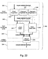
- the arrangement 201 includes a standard host computer system which takes the form of a host CPU 202 interconnected to its own memory store (RAM) 203 via a bridge 204.
- the host computer system provides all the normal facilities of a computer system including operating systems programs, applications, display of information, etc.
- the host computer system is connected to a standard PCI bus 206 via a PCI bus interface 207.
- the PCI standard is a well known industry standard and most computer systems sold today, particularly those running Microsoft Windows (trade mark) operating systems, normally come equipped with a PCI bus 206.
- the PCI bus 206 allows the arrangement 201 to be expanded by means of the addition of one or more PCI cards, eg. 209, each of which contain a further PCI bus interface 210 and other devices 211 and local memory 212 for utilization in the arrangement 201.
- a raster image accelerator card 220 to assist in the speeding up of graphical operations expressed in a page description language.
- the raster image accelerator card 220 (also having a PCI bus interface 221) is designed to operate in a loosely coupled, shared memory manner with the host CPU 202 in the same manner as other PCI cards 209. It is possible to add further image accelerator cards 220 to the host computer system as required.
- the raster image accelerator card is designed to accelerate those operations that form the bulk of the execution complexity in raster image processing operations. These can include:
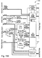
- the raster image accelerator card 220 further includes its own local memory 223 connected to a raster image co-processor 224 which operates the raster image accelerator card 220 generally under instruction from the host CPU 202.
- the co-processor 224 is preferably constructed as an Application Specific Integrated Circuit (ASIC) chip.
- ASIC Application Specific Integrated Circuit
- the raster image co-processor 224 includes the ability to control at least one printer device 226 as required via a peripheral interface 225.
- the image accelerator card 220 may also control any input/output device, including scanners. Additionally, there is provided on the accelerator card 220 a generic external interface 227 connected with the raster image co-processor 224 for its monitoring and testing.
- the host CPU 202 sends, via PCI bus 206, a series of instructions and data for the creation of images by the raster image co-processor 224.
- the data can be stored in the local memory 223 in addition to a cache 230 in the raster image co-processor 224 or in registers 229 also located in the co-processor 224.
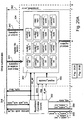
- the co-processor 224 is responsible for the acceleration of the aforementioned operations and consists of a number of components generally under the control of an instruction controller 235.
- a local memory controller 236 for communications with the local memory 223 of Fig. 1.
- a peripheral interface controller 237 is also provided for the communication with printer devices utilising standard formats such as the Centronics interface standard format or other video interface formats.
- the peripheral interface controller 237 is interconnected with the local memory controller 236. Both the local memory controller 236 and the external interface controller 238 are connected with an input interface switch 252 which is in turn connected to the instruction controller 235.
- the input interface switch 252 is also connected to a pixel organizer 246 and a data cache controller 240.
- the input interface switch 252 is provided for switching data from the external interface controller 238 and local memory controller 236 to the instruction controller 235, the data cache controller 240 and the pixel organizer 246 as required.
- the external interface controller 238 is provided in the raster image co-processor 224 and is connected to the instruction controller 235. There is also provided a miscellaneous module 239 which is also connected to the instruction controller 235 and which deals with interactions with the co-processor 224 for purposes of test diagnostics and the provision of clocking and global signals.
- the data cache 230 operates under the control of the data cache controller 240 with which it is interconnected.
- the data cache 230 is utilized in various ways, primarily to store recently used values that are likely to be subsequently utilized by the co-processor 224.
- the aforementioned acceleration operations are carried out on plural streams of data primarily by a JPEG coder/decoder 241 and a main data path unit 242.
- the units 241. 242 are connected in parallel arrangement to all of the pixel organizer 246 and two operand organizers 247, 248.
- the processed streams from units 241, 242 are forwarded to a results organizer 249 for processing and reformatting where required. Often, it is desirable to store intermediate results close at hand. To this end.
- a multi-used value buffer 250 is provided. interconnected between the pixel organizer 246 and the result organizer 249. for the storage of intermediate data.
- the result organizer 249 outputs to the external interface controller 238. the local memory controller 236 and the peripheral interface controller 237 as required.
- a further (third) data path unit 243 can, if required be connected "in parallel" with the two other data paths in the form of JPEG coder/decoder 241 and the main data path unit 242.
- the extension to 4 or more data paths is achieved in the same way. Although the paths are "parallel" connected, they do not operate in parallel. Instead only one path at a time operates.
- the first step was the realization that in image manipulation often repetitive calculations of the same basic type were required to be carried out.
- a calculating unit could be configured to carry out a specific type of calculation, a long stream of data processed and then the calculating unit could be reconfigured for the next type of calculation step required. If the data streams were reasonably long, then the time required for reconfiguration would be negligible compared to the total calculation time and thus throughput would be enhanced.
- the provision of plural data processing paths means that in the event that one path is being reconfigured whilst the other path is being used, then there is substantially no loss of calculating time due to the necessary reconfiguration.
- the main data path unit 242 carries out a more general calculation and the other data path(s) carry out more specialized calculation such as JPEC coding and decoding as in unit 241 or, if additional unit 243 is provided, it can provide entropy and/or Huffman coding/decoding.
- the fetching and presenting of data to the calculating unit can be proceeding. This process can be further speeded up, and hardware resources better utilized, if the various types of data are standardized or normalized in some way. Thus the total overhead involved in fetching and despatching data can be reduced.
- the co-processor 224 operates under the control of host CPU 202 (Fig. 1).
- the instruction controller 235 is responsible for the overall control of the co-processor 224.
- the instruction controller 235 operates the co-processor 224 by means of utilising a control bus 231, hereinafter known as the CBus.
- the CBus 231 is connected to each of the modules 236-250 inclusive to set registers (231 of Fig. 1) within each module so as to achieve overall operation of the co-processor 224.
- the interconnection of the control bus 231 to each of the modules 236-250 is omitted from Fig 2.
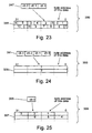
- FIG. 3 there is illustrated a schematic layout 260 of the available module registers.
- the layout 260 includes registers 261 dedicated to the overall control of the co-processor 224 and its instruction controller 235.
- the co-processor modules 236-250 include similar registers 262.
- Modern computer systems typically require some method of memory management to provide for dynamic memory allocation.
- some method is necessary to synchronize between the dynamic allocation of memory and the use of that memory by a co-processor.
- a computer hardware configuration has both a CPU and a specialized co-processor, each sharing a bank of memory.
- the CPU is the only entity in the system capable of allocating memory dynamically. Once allocated by the CPU for use by the co-processor, this memory can be used freely by the co-processor until it is no longer required, at which point it is available to be freed by the CPU. This implies that some form of synchronization is necessary between the CPU and the co-processor in order to ensure that the memory is released only after the co-processor is finished using it. There are several possible solutions to this problem but each has undesirable performance implications.
- statically allocated memory avoids the need for synchronization, but prevents the system from adjusting its memory resource usage dynamically. Similarly, having the CPU block and wait until the co-processor has finished performing each operation is possible, but this substantially reduces parallelism and hence reduces overall system performance.
- interrupts to indicate completion of operations by the co-processor is also possible but imposes significant processing overhead if co-processor throughput is very high.
- Fig. 4 the preferred arrangement for synchronising the (host) CPU and the co-processor is illustrated in Fig. 4 where the reference numerals used are those already utilized in the previous description of Fig. 1.
- the CPU 202 is responsible for all memory management in the system. It allocates memory 203 both for its own uses, and for use by the co-processor 224.
- the co-processor 224 has its own graphics-specific instruction set, and is capable of executing instructions 1022 from the memory 203 which is shared with the host processor 202. Each of these instructions can also write results 1024 back to the shared memory 203, and can read operands 1023 from the memory 203 as well.
- the amount of memory 203 required to store operands 1023 and results 1024 of co-processor instructions varies according to the complexity and type of the particular operation.
- the CPU 202 is also responsible for generating the instructions 1022 executed by the co-processor 224. To maximize the degree of parallelism between the CPU 202 and the co-processor 224, instructions generated by the CPU 202 are queued as indicated at 1022 for execution by the co-processor 224. Each instruction in the queue 1022 can reference operands 1023 and results 1024 in the shared memory 203, which has been allocated by the host CPU 202 for use by the co-processor 224.
- the method utilizes an interconnected instruction generator 1030, memory manager 1031 and queue manager 1032, as shown in Fig. 5. All these modules execute in a single process on the host CPU 202.
- Instructions for execution by the co-processor 224 are generated by the instruction generator 1030, which uses the services of the memory manager 1031 to allocate space for the operands 1023 and results 1024 of the instructions being generated.
- the instruction generator 1030 also uses the services of the queue manager 1032 to queue the instructions for execution by the co-processor 224.
- the CPU 202 can free the memory which was allocated by the memory manager 1031 for use by the operands of that instruction.
- the result of one instruction can also become an operand for a subsequent instruction, after which its memory can also be freed by the CPU.
- the system frees the resources needed by each instruction via a cleanup function which runs at some stage after the co-processor 224 has completed the instruction. The exact time at which these cleanups occur depends on the interaction between the memory manager 1031 and the queue manager 1032, and allows the system to adapt dynamically according to the amount of system memory available and the amount of memory required by each co-processor instruction.
- Fig. 6 schematically illustrates the implementation of the co-processor instruction queue 1022. Instructions are inserted into a pending instruction queue 1040 by the host CPU 202, and are read by the co-processor 224 for execution. After execution by the co-processor 224. the instructions remain on a cleanup queue 1041. so that the CPU 202 can release the resources that the instructions required after the co-processor 224 has finished executing them.
- the instruction queue 1022 itself can be implemented as a fixed or dynamically sized circular buffer.
- the instruction queue 1022 decouples the generation of instructions by the CPU 202 from their execution by the co-processor 224.
- Operand and result memory for each instruction is allocated by the memory manager 1031 (Fig. 5) in response to requests from the instruction generator 1030 during instruction generation. It is the allocation of this memory for newly generated instructions which triggers the interaction between the memory manager 1031 and the queue manager 1032 described below, and allows the system to adapt automatically to the amount of memory available and the complexity of the instructions involved.
- the instruction queue manager 1032 is capable of waiting for the co-processor 224 to complete the execution of any given instruction which has been generated by the instruction generator 1030.
- the instruction queue manager 1032 by providing a sufficiently large instruction queue 1022 and sufficient memory 203 for allocation by the memory manager 1031, it becomes possible to avoid having to wait for the co-processor 224 at all, or at least until the very end of the entire instruction sequence, which can be several minutes on a very large job.
- peak memory usage can easily exceed the memory available, and at this point the interaction between the queue manager 1032 and the memory manager 1031 comes into play.
- the instruction queue manager 1032 can be instructed at any time to "cleanup" the completed instructions by releasing the memory that was dynamically allocated for them. If the memory manager 1031 detects that available memory is either running low or is exhausted, its first recourse is to instruct the queue manager 1032 to perform such a cleanup in an attempt to release some memory which is no longer in use by the co-processor 224. This can allow the memory manager 1031 to satisfy a request from the instruction generator 1030 for memory required by a newly generated instruction, without the CPU 202 needing to wait for, or synchronize with, the co-processor 224.
- the memory manager 1031 can request that the queue manager 1032 wait for a fraction, say half, of the outstanding instructions on the pending instruction queue 1040 to complete. This will cause the CPU 202 processing to block until some of the co-processor 224 instructions have been completed, at which point their operands can be freed, which can release sufficient memory to satisfy the request. Waiting for only a fraction of the outstanding instructions ensures that the co-processor 224 is kept busy by maintaining at least some instructions in its pending instruction queue 1040. In many cases the cleanup from the fraction of the pending instruction queue 1040 that the CPU 202 waits for, releases sufficient memory for the memory manager 1031 to satisfy the request from the instruction generator 1030.
- the final recourse of the memory manager 1031 is to wait until all pending co-processor instructions have completed. This should release sufficient resources to satisfy the request of the instruction generator 1030, except in the case of extremely large and complex jobs which exceed the system's present memory capacity altogether.
- the system effectively tunes itself to maximize throughput for the given amount of memory 203 available to the system. More memory results in less need for synchronization and hence greater throughput. Less memory requires the CPU 202 to wait more often for the co-processor 224 to finish using the scarce memory 203, thereby yielding a system which still functions with minimal memory available, but at a lower performance.
- the steps taken by the memory manager 1031 when attempting to satisfy a request from the instruction generator 1030 are summarized below. Each step is tried in sequence, after which the memory manager 1031 checks to see if sufficient memory. 203 has been made available to satisfy the request. If so, it stops because the request can be satisfied; otherwize it proceeds to the next step in a more aggressive attempt to satisfy the request:
- Fig. 7 in addition to the interaction between the memory manager 1031 and the queue manager 1032. the queue manager 1032 can also initiate a synchronization with the co-processor 224 in the case where space in a fixed-length instruction queue buffer 1050 is exhausted. Such a situation is depicted in Fig. 7.
- the pending instructions queue 1040 is ten instructions in length. The latest instruction to be added to the queue 1040 has the highest occupied number. Thus where space is exhausted the latest instruction is located at position 9. The next instruction to be input to the co-processor 224 is waiting at position zero.
- the queue manager 1032 will also wait for, say, half the pending instructions to be completed by the co-processor 224. This delay normally allows sufficient space in the instruction queue 1040 to be freed for new instructions to be inserted by the queue manager 1032.
- the method used by the queue manager 1032 when scheduling new instructions is as follows:
- the method used by the queue manager 1032 when asked to wait for a given instruction is as follows:
- the method used by the instruction generator 1030 when issuing new instructions is as follows:
- the co-processor 224 maintains various registers 261 for the execution of each instruction stream.
- Table 1 sets out the name, type and description of each of the registers utilized by the co-processor 224.
- Table 1 Register Description NAME TYPE DESCRIPTION External Interface Controller Registers eic_cfg Config2 Configuration eic_stat Status Status eic_err_int Interrupt Error and Interrupt Status eic_err_int_en Config2 Error and Interrupt Enable eic_test Config2 Test modes eic_gen_pob Config2 Generic bus programmable output bits elc_high_addr Config1 Dual address cycle offset etc_wtlb_v Control2 Virtual address and operation bits for TLB Invalidate/Write elc_wtlb_p Config2 Physical address and control bits for TLB Write eic_mmu_v Status Most recent MMU virtual address translated, and current LRU location.
- eic_mmu_v Status Most recent page table physical address fetched by MMU.
- eic_ip_addr Status Physical address for most recent IBus access to the PCI Bus.
- eic_rp_addr Status Physical address for most recent RBus access to the PCI Bus.
- eic_ig_addr Status Address for most recent IBus access to the Generic Bus.
- eic_rg_data Status Address for most recent RBus access to the Generic Bus.
- pci_external_cfg Status 32-bit field downloaded at reset from an external serial ROM. Has no influence on coprocessor operation.
- the co-processor 224 in order to maximize the utilization of its resources and to provide for rapid output on any external peripheral device, executes one of two independent instruction streams.
- one instruction stream is associated with a current output page required by an output device in a timely manner, while the second instruction stream utilizes the modules of the co-processor 224 when the other instruction stream is dormant.
- the overriding imperatives are to provide the required output data in a timely manner whilst simultaneously attempting to maximize the use of resources for the preparation of subsequent pages, bands, etc.
- the co-processor 224 is therefore designed to execute two completely independent but identically implemented instruction streams (hereafter termed A and B).
- the instructions are preferably generated by software running on the host CPU 202 (Fig.
- One of the instruction streams (stream A) operates at a higher priority than the other instruction stream (stream B) during normal operation.
- the stream or queue of instructions is written into a buffer or list of buffers within the host RAM 203 (Fig. 1) by the host CPU 202.
- the buffers are allocated at start-up time and locked into the physical memory of the host 203 for the duration of the application.
- Each instruction is preferably stored in the virtual memory environment of the host RAM 203 and the raster image co-processor 224 utilizes a virtual to physical address translation scheme to determine a corresponding physical address with the in-host RAM 203 for the location of a next instruction.
- These instructions may alternatively be stored in the co-processors 224 local memory.
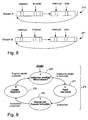
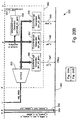
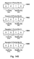
- FIG. 8 there is illustrated the format of two instruction streams A and B 270, 271 which are stored within the host RAM 203.
- the format of each of the streams A and B is substantially identical.
- the execution model for the co-processor 224 consists of:
- the instruction controller 235 is responsible for implementing the co-processor's instruction execution model maintaining overall executive control of the co-processor 224 and fetching instructions from the host RAM 203 when required. On a per instruction basis, the instruction controller 235 carries out the instruction decoding and configures the various registers within the modules via CBus 231 to force the corresponding modules to carry-out that instruction.
- the instruction execution cycle consists of four main stages 276-279.
- the first stage 276 is to determine if an instruction is pending on any instruction stream. If this is the case, an instruction is fetched 277, decoded and executed 278 by means of updating registers 279.
- the instruction controller 235 will "spin" or idle until a pending instruction is found.
- the Instruction Controller 235 fetches the instruction using the address in the corresponding instruction pointer register (ic_ipa or ic_ipb). However, the Instruction Controller 235 does not fetch an instruction if a valid instruction already exists in a prefetch buffer stored within the instruction controller 235.
- a valid instruction is in the prefetch buffer if ⁇
- the validity of the contents of the prefetch buffer is indicated by a prefetch bit in the ic_stat register, which is set on a successful instruction prefetch. Any external write to any of the registers of the instruction controller 235 causes the contents of the prefetch buffer to be invalidated.
- the instruction controller 235 decodes it and configures the registers 229 of the co-processor 224 to execute the instruction.
- the instruction format utilized by the raster image co-processor 224 differs from traditional processor instruction sets in that the instruction generation must be carried out instruction by instruction by the host CPU 202 and as such is a direct overhead for the host. Further, the instructions should be as small as possible as they must be stored in host RAM 203 and transferred over the PCI bus 206 of Fig. 1 to the co-processor 224. Preferably, the co-processor 224 can be set up for operation with only one instruction. As much flexibility as possible should be maintained by the instruction set to maximize the scope of any future changes. Further, preferably any instruction executed by the co-processor 224 applies to a long stream of operand data to thereby achieve best performance.
- the co-processor 224 employs an instruction decoding philosophy designed to facilitate simple and fast decoding for "typical instructions” yet still enable the host system to apply a finer control over the operation of the co-processor 224 for "atypical" operations.
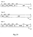
- FIG. 10 there is illustrated the format of a single instruction 280 which comprizes eight words each of 32 bits.
- Each instruction includes an instruction word or opcode 281, and an operand or result type data word 282 setting out the format of the operands.
- the addresses 283-285 of three operands A. B and C are also provided, in addition to a result address 286 Further, an area 287 is provided for use by the host CPU 202 for storing information relevant to the instruction.
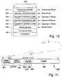
- the structure 290 of an instruction opcode 281 of an instruction is illustrated in Fig. 11.
- the instruction opcode is 32 bits long and includes a major opcode 291, a minor opcode 292, an interrupt (I) bit 293, a partial decode (Pd) bit 294, a register length (R) bit 295, a lock (L) bit 296 and a length 297.
- a description of the fields in the instruction word 290 is as provided by the following table.
- the instruction can be coded such that instruction execution sets an interrupt and pause on completion of that instruction. This interrupt is called an "instruction completed interrupt".
- the partial decode bit 294 provides for a partial decode mechanism such that when the bit is set and also enabled in the ic_cfg register, the various modules can be micro coded prior to the execution of the instruction in a manner which will be explained in more detail hereinafter.
- the lock bit 296 can be utilized for operations which require more than one instruction to set up. This can involve setting various registers prior to an instruction and provides the ability to "lock" in the current instruction stream for the next instruction.
- the length field 297 has a natural definition for each instruction and is defined in terms of the number of "input data items” or the number of "output data items” as required.
- the length field 297 is only 16 bits long. For instructions operating on a stream of input data items greater than 64,000 items the R-bit 295 can be set, in which case the input length is taken from a po_len register within the pixel organizer 246 of Fig. 2. This register is set immediately before such an instruction.
- Table 3 Operand Types Instruction Class Length defined by # of operands Compositing input pixels 3 General Color Space Conversion input pixels 3 JPEG decompression/compression input bytes 2 other decompression/compression input bytes 2 Image Transformations and Convolutions output bytes 2 Matrix Multiplication input pixels 2 Halftoning input pixels, bytes 2 Memory Copying input pixels, bytes 1 Hierarchial Image Decompression input pixels, bytes 1 or 2 Flow Control fixed fixed fixed fixed fixed fixed fixed 4
- Fig. 12 there is illustrated, firstly, the data word format 300 of the data word or operand descriptor 282 of Fig. 10 for three operand instructions and, secondly, the data word format 301 for two operand instructions.
- the co-processor 224 is set up to fetch, or otherwize calculate, one internal data item, and use this item for the length of the instruction for that operand.
- the co-processor 224 is set up to cycle through a small set of data producing a "tiling effect". When the L-bit of an operand descriptor is zero then the data is immediate, ie. the data items appear literally in the operand word.
- each of the operand and result words 283-286 contains either the value of the operand itself or a 32-bit virtual address to the start of the operand or result where data is to be found or stored.
- the instruction controller 235 of Fig. 2 proceeds to decode the instruction in two stages. It first checks to see whether the major opcode of the instruction is valid, raising an error if the major opcode 291 (Fig. 11) is invalid. Next, the instruction is executed by the instruction controller 235 by means of setting the various registers via CBus 231 to reflect the operation specified by the instruction. Some instructions can require no registers to be set.
- the registers for each module can be classified into types based on their behavior. Firstly, there is the status register type which is "read only” by other modules and “read/write” by the module including the register. Next, a first type of configuration register, hereinafter called “config1 ", is “read/write” externally by the modules and “read only” by the module including the register. These registers are normally used for holding larger type configuration information, such as address values. A second type of configuration register, herein known as “config2”, is readable and writable by any module but is read only by the module including the register. This type of register is utilized where bit by bit addressing of the register is required.
- control1 registers A number of control type registers are provided.
- a first type hereinafter known as “control1” registers, is readable and writable by all modules (including the module which includes the register).
- the control1 registers are utilized for holding large control information such as address values.
- control2 a second type of control register, hereinafter known as “control2”, which can be set on a bit by bit basis.
- a final type of register known as an interrupt register has bits within the register which are settable to 1 by the module including the register and resettable to zero externally by writing a "1" to the bit that has been set. This type of register is utilized for dealing with the interrupts/errors flagged by each of the modules.
- Each of the modules of the co-processor 224 sets a c_active line on the CBus 231 when it is busy executing an instruction.
- the instruction controller 235 can then determine when instructions have been completed by "OR-ing" the c_active lines coming from each of the modules over the CBus 231.
- the local memory controller module 236 and the peripheral interface controller module 237 are able to execute overlapped instructions and include a c_background line which is activated when they are executing an overlapped instruction.
- the overlapped instructions are "local DMA" instructions transferring data between the local memory interface and the peripheral interface.
- the execution cycle for an overlapped local DMA instruction is slightly different from the execution cycle of other instructions. If an overlapped instruction is encountered for execution, the instruction controller 235 checks whether there is already an overlapped instruction executing. If there is, or overlapping is disabled, the instruction controller 235 waits for that instruction to finish before proceeding with execution of that instruction. If there is not, and overlapping is enabled, the instruction controller 235 immediately decodes the overlapped instruction and configures the peripheral interface controller 237 and local memory controller 236 to carry out the instruction. After the register configuration is completed, the instruction controller 235 then goes on to update its registers (including finished register, status register, instruction pointer, etc.) without waiting for the instruction to "complete" in the conventional sense. At this moment, if the finished sequence number equals the interrupt sequence number, 'the overlapped instruction completed' interrupt is primed rather than raising the interrupt immediately. The overlapped instruction completed' interrupt is raized when the overlapped instruction has fully completed.
- the instruction controller attempts to prefetch the next instruction while the current instruction is executing. Most instructions take considerably longer to execute than they will to fetch and decode.
- the instruction controller 235 prefetches an instruction if all of the following conditions are met:
- the instruction controller 235 determines that prefetching is possible it requests the next instruction, places it in a prefetch buffer and then validates the buffer. At this point there is nothing more for the instruction controller 235 to do until the currently executing instruction has completed.
- the instruction controller 235 determines the completion of an instruction by examining the c_active and c_background lines associated with the CBus 231.
- the instruction controller 235 Upon completion of an instruction, the instruction controller 235 updates its registers to reflect the new state. This must be done atomically to avoid problems with synchronising with possible external accesses. This atomic update process involves:
- the Register Access Semaphore is a mechanism that provides atomic accesses to multiple instruction controller registers.
- the registers that can require atomic access are as follows:
- External agents can read all registers safely at any time. External agents are able to write any registers at any time, however to ensure that the Instruction Controller 235 does not update values in these registers, the external agent must first obtain the Register Access Semaphore. The Instruction Controller does not attempt to update any values in the abovementioned registers if the Register Access Semaphore is claimed externally. The instruction controller 235 updates all of the above mentioned registers in one clock cycle to ensure atomicity.
- each instruction has associated with it a 32 bit "sequence number”. Instruction sequence numbers increment wrapping through from OxFFFFFF to 0x00000000.
- External agents can set any of the interrupt primed bits (bits a_primed, a_ol_primed. b_primed or b_ol_primed) in the status register to activate or de-activate this interrupt mechanism independently.
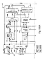
- the instruction controller 235 includes an execution controller 305 which implements the instruction execution cycle as well as maintaining overall executive control of the co-processor 224.
- the functions of the execution controller 305 include maintaining overall executive control of the instruction controller 235, determining instructing sequencing, instigating instruction fetching and prefetching, initiating instructing decoding and updating the instruction controller registers.
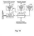
- the instruction controller further includes an instruction decoder 306.
- the instruction decoder 306 accepts instructions from a prefetch buffer controller 307 and decodes them according the aforementioned description.
- the instruction decoder 306 is responsible for configuring registers in the other co-processor modules to execute the instruction.
- the prefetch buffer controller 307 manages the reading and writing to a prefetch buffer within the prefetch buffer controller and manages the interfacing between the instruction decoder 306 and the input interface switch 252 (Fig. 2).
- the prefetch buffer controller 307 is also responsible for managing the updating of the two instruction pointer registers (ic_ipa and ic_ipb).
- Access to the CBus 231 (Fig. 2) by the instruction controller 235, the miscellaneous module 239 (Fig. 2) and the external interface controller 238 (Fig. 2) is controlled by a "CBus" arbitrator 308 which arbitrates between the three modules' request for access.
- the requests are transferred by means of a control bus (CBus) 231 to the register units of the various modules.
- CBus control bus
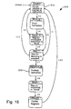
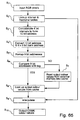
- Fig. 14 there is illustrated the execution controller 305 of Fig. 13 in more detail.
- the execution controller is responsible for implementing the instruction execution cycle 275 of Fig. 9 and, in particular, is responsible for:
- the execution controller includes a large core state machine 310 hereinafter known as "the central brain" which implements the overall instruction execution cycle.
- the execution controller includes an instruction prefetch logic unit 311. This unit is responsible for determining whether there is an outstanding instruction to be executed and which instruction stream the instruction belongs to.
- the start 312 and prefetch 313 states of the transition diagram of Fig. 15 utilize this information in obtaining instructions.
- a register management unit 317 of Fig. 14 is responsible for monitoring the register access semaphores on both instruction streams and updating all necessary registers in each module.
- the register management unit 317 is also responsible for comparing the finished register (ic_fna or ic_fnb) with the interrupt register (ic_inta or ic_intb) to determine if a "sequence number compieted" interrupt is due.
- the register management unit 317 is also responsible for interrupt priming.
- An overlapped instructions unit 318 is responsible for managing the finishing off of an overlapped instruction through management of the appropriate status bits in the ic_stat register.
- the execution controller also includes a decoder interface unit 319 for interfacing between the central brain 310 and the instruction decoder 306 of Fig. 13.
- the instruction decoder 306 is responsible for configuring the co-processor to execute the instructions residing in the prefetch buffer.
- the instruction decoder 306 includes an instruction decoder sequencer 321 which comprizes one large state machines broken down into many smaller state machines.
- the instruction sequencer 321 communicates with a CBus dispatcher 312 which is responsible for setting the registers within each module.
- the instruction decoder sequencer 321 also communicates relevant information to the execution controller such as instruction validity and instruction overlap conditions.
- the instruction validity check being to check that the instruction opcode is not one of the reserved opcodes.
- the instruction dispatch sequencer 321 includes a overall sequencing control state machine 324 and a series of per module configuration sequencer state machines, eg. 325, 326.
- One per module configuration sequencer state machine is provided for each module to be configured.
- Collectively the state machines implement the co-processor's microprogramming of the modules.
- the state machines, eg. 325 instruct the CBus dispatcher to utilize the global CBus to set various registers so as to configure the various modules for processing.
- a side effect of writing to particular registers is that the instruction execution commences. Instruction execution typically takes much longer than the time it takes for the sequencer 321 to configure the co-processor registers for execution.
- the Instruction Decode Sequencer 321 does not configure all of the modules within the co-processor for every instruction.
- the table below shows the ordering of module configuration for each class of instruction with the module configured including the pixel organizer 246 (PO), the data cache controller 240 (DCC), the operand organizer B 247 (OOB), the operand organizer C 248 (OOC), main data path 242 (MDP), results organizer 249 (RO), and JPEG encoder 241 (JC).
- Some of the modules are never configured during the course of instruction decoding. These modules are the External Interface Controller 238 (EIC), the Local Memory Controller 236 (LMC), the Instruction Controller 235 itself (IC), the Input Interface Switch 252 (IIS) and the Miscellaneous Module (MM).
- Module Setup Order Instruction Class Module Configuration Sequence Sequence ID Compositing PO, DCC, OOB, OOC, MDP, RO 1 CSC PO, DCC, OOB, OOC, MDP, RO 2 JPEG coding PO, DCC, OOB, OOC, JC, RO 3 Data coding PO, DCC, OOB, OOC, JC, RO 3 Transformations and Convolutions PO, DCC, OOB, OOC, MDP, RO 2 Matrix Multiplication PO, DCC, OOB, OOC, MDP, RO 2 Halftoning PO, DCC, OOB, MDP, RO 4 General memory copy PO, JC, RO 8 Peripheral DMA PIC 5 Hierarchial Image - Horizontal Interpolation PO, DCC, OOB, OOC, MDP, RO 6 Hierarchial Image - others PO, DCC, OOB, OOC, MDP, RO 4 Internal access RO, RO, RO, RO, RO 7 others - - -
- each of the module configuration sequencers, eg. 325 is responsible for carrying out the required register access operations to configure the particular module.
- the overall sequencing control state machine 324 is responsible for overall operation of the module configuration sequencer in the aforementioned order.
- Fig. 18. there is illustrated 330 the state transition diagram for the overall sequencing control unit which basically activates the relevant module configuration sequencer in accordance with the above table.
- Each of the modules configuration sequencers is responsible for controlling the CBus dispatcher to alter register details in order to set the various registers in operation of the modules.
- the prefetch buffer controller consists of a prefetch buffer 335 for the storage of a single co-processor instruction (six times 32 bit words).
- the prefetch buffer includes one write port controlled by a IBus sequencer 336 and one read port which provides data to the instruction decoder, execution controller and the instruction controller CBus interface.
- the IBus sequencer 336 is responsible for observing bus protocols in the connection of the prefetch buffer 335 to the input interface switch.
- An address manager unit 337 is also provided which deals with address generation for instruction fetching.
- the address manager unit 337 performs the functions of selecting one of ic_ipa or ic_ipb to place on the bus to the input interface switch, incrementing one of ic_ipa or ic_ipb based on which stream the last instructions was fetched from and channelling jump target addresses back to the ic_ipa and ic_ipb register.
- a PBC controller 339 maintains overall control of the prefetched buffer controller 307.
- each module including the instruction controller module itself, has an internal set of registers 304 as previously defined in addition to a CBus interface controller 303 as illustrated in Fig. 20 and which is responsible for receiving CBus requests and updating internal registers in light of those requests.
- the module is controlled by writing registers 304 within the module via a CBus interface 302.
- a CBus arbitrator 308 (Fig. 13) is responsible for determining which module of the instruction controller 235, the external interface controller or the miscellaneous module is able to control the CBus 309 for acting as a master of the CBus and for the writing or reading of registers.
- Fig. 20 illustrates, in more detail, the standard structure of a CBus interface 303 as utilized by each of the modules.
- the standard CBus interface 303 accepts read and write requests from the CBus 302 and includes a register file 304 which is utilized 341 and updated on 341 by the various submodules within a module. Further, control lines 344 are provided for the updating of any submodule memory areas including reading of the memory areas.
- the standard CBus interface 303 acts as a destination on the CBus, accepting read and write requests for the register 304 and memory objects inside other submodules.
- a "c_reset” signal 345 sets every register inside the Standard CBus interface 103 to their default states. However, “c_reset” will not reset the state machine that controls the handshaking of signals between itself and the CBus Master, so even if “c_reset” is asserted in the middle of a CBus transaction, the transaction will still finish, with undefined effects.
- the signals "c_sdata_in” 345 and “c_svalid_in” are data and valid signals from the previous module in a daisy chain of modules.
- the signals “c_sdata_out” and “c_svalid_out” 350 are data and valid signals going to the next module in the daisy chain.
- the functionality of the Standard CBus interface 303 includes:
- the Standard CBus Interface 303 accepts register read/write and bit set requests that appears on the CBus. There are two types of CBus instructions that Standard CBus Interface handles:
- Type A operations allow other modules to read or write 1, 2, 3, or 4 bytes into any register inside Standard CBus Interface 303.
- the data cycle occurs in the clock cycle immediately after the instruction cycle. Note that the type field for register write and read are "1000" and "1001" respectively.
- the Standard CBus Interface 303 decodes the instruction to check whether the instruction is addressed to the module, and whether it is a read or write operation. For read operation, the Standard CBus Interface 303 uses the "reg" field of the CBus transaction to select which register output is to put into the "c_sdata" bus 350. For write operations, the Standard CBus Interface 303 uses the “reg” and “byte” fields to write the data into the selected register. After read operation is completed, the Standard CBus Interface returns the data and asserts "c_svalid" 350 at the same time. After write operations are completed, the Standard CBus Interface 303 asserts "c_svalid" 350 to acknowledge.
- Type C operations allow other modules to write one or more bits in one of the bytes in one of the registers. Instruction and data are packed into one word.
- the Standard CBus Interface 303 decodes the instruction to check whether the instruction is addressed to the module. It also decodes "reg", "byte” and “enable” fields to generate the required enable signals. It also latches the data field of the instruction, and distributes it to all four bytes of a word so the required bit(s) are written in every enabled bit(s) in every enabled byte(s). No acknowledgment is required for this operation.
- the Standard CBus Interface 303 accepts memory read and memory write requests that appears on the CBus. While accepting a memory read/write request, the Standard CBus Interface 303 checks whether the request is addressed to the module. Then, by decoding the address field in the instruction, the Standard CBus Interface generates the appropriate address and address strobe signals 344 to the submodule which a memory read/write operation is addressed to. For write operations the Standard CBus Interface also passes on the byte enable signals from the instruction to the submodules.
- the operation of the standard CBus interface 303 is controlled by a read/write controller 352 which decodes the type field of a CBus instruction from the CBus 302 and generates the appropriate enable signals to the register file 304 and output selector 353 so that the data is latched on the next cycle into the register file 304 or forwarded to other submodules 344. If the CBus instruction is a register read operation, the read/write controller 352 enables the output selector 353 to select the correct register output going onto the "c_sdata bus" 345. If the instruction is a register write operation, the read/write controller 352 enables the register file 304 to select the data in the next cycle.
- the register file 304 contains four parts, being a register select decoder 355. an output selector 353, interrupt 356. error 357 and exception 358 generators, unmasked error generator 359 and the register components 360 which make up the registers of that particular module.
- the register select decoder 355 decodes the signal "ref_en” (register file enable), "write” and “reg” from the read/write controller 352 and generates the register enable signals for enabling the partictilar register of interest.
- the output selector 353 selects the correct register data to be output on c_sdata_out lines 350 for register read operations according to the signal "reg" output from the read/write controller 352.
- the exception generators 356-359 generate an output error signal, eg. 347-349. 362 when an error is detected on their inputs.
- the formula for calculating each output error is as aforementioned.
- the register components 360 can be defined to be of a number of types in accordance with requirements as previously discussed when describing the structure of the register set with reference to Table 5.
- the CBus (control bus) is responsible for the overall control of each module by way transferring information for the setting of registers within each module's standard CBus interface. It will be evident from the description of the standard CBus interface that the CBus serves two main purposes:
- the CBus uses an instruction-address-data protocol to control modules by the setting configuration registers within the modules. In general, registers will be set on a per instruction basis but can be modified at any time.
- the CBus gathers status and other information, and accesses RAM and FIFO data from the various modules by requesting data
- the CBus is driven on a transaction by transaction basis either by:
- the driving module is considered to be the source module of the CBus, and all other modules possible destinations. Arbitration on this bus is carried out by the Instruction Controller.
- a CBus c_iad signal contains the addressing data and is driven by the controller in two distinct cycles:
- the data associated with an instruction is placed on the c_iad bus in the cycle directly following the instruction cycle.
- the target module of the read operation drives the c_sdata signal until the data cycle completes.
- the bus includes a 32 bit instruction-address-data field which can be one of three types 370-372:
- each instruction encodes the relevant CBus transaction type in accordance with the following table: Table 7: CBus Transaction Types c_iad.type value transaction type instruction format type 0000 no-op A, B, C 0001 reserved 0010 peripheral interface write B 0011 peripheral interface read B 0100 generic bus write B 0101 generic bus read B 0110 local memory write B 0111 local memory read B 1000 register write A 1001 register read A 1010 module memory write A 1011 module memory read A 1100 test mode write A 1101 test mode read A 1110 bit set C 1111 reserved
- the byte field is utilized for enabling bits within a register to be set.
- the module field sets out the particular module to which an instruction on the CBus is addressed.
- the register field sets out which of the registers within a module is to be updated.
- the address field is utilized for addressing memory portions where an operation is desired on those memory portions and can be utilized for addressing RAMs. FIFOs, etc.
- the enable field enables selected bits within a selected byte when a bit set instruction is utilized.
- the data field contains the bit wize data of the bits to be written to the byte selected for update.
- the CBus includes a c_active line for each module, which is asserted when ever a module has outstanding activity pending.
- the instruction controller utilizes these signals to determine when an instruction has completed.
- the CBus contains a c_background line for each module that can operate in a background mode in addition to any preset, error and interrupt lines, one for each module, for resetting, detecting errors and interrupts.
- a computer graphics processor having three main functional blocks: a data normalizer 1062 which may be implemented in each of the pixel organizer 246 and operand organizers B and C 247, 248, a central graphics engine in the form of the main data path 242 or JPEG units 241 and a programming agent 1064, in the form of an instruction controller 235.
- the operation of the data normalizer 1062 and the central graphics engine 1064 is determined by an instruction stream 1066 that is provided to the programming agent 1064.
- the programming agent 1064 For each instruction, the programming agent 1064 performs a decoding function and outputs internal control signals 1067 and 1068 to the other blocks in the system.
- the normalizer 1062 will format the data according to the current instruction and pass the result to the central graphics engine 1063, where further processing is performed.
- the data normalizer represents, in a simplified form, the pixel organizer and the operand organizers B and C. Each of these organizers implements the data normalization circuitry, thereby enabling appropriate normalization of the input data prior to it passing to the central graphics engine in the form of the JPEG coder or the main data path.
- the central graphics engine 1063 operates on data that is in a standard format, which in this case is 32-bit pixels.
- the normalizer is thus responsible for converting its input data to a 32-bit pixel format.
- the input data words 1069 to the normalizer are also 32 bits wide, but may take the form of either packed components or unpacked bytes.
- a packed component input stream consists of consecutive data objects within a data word, the data objects being 1,2,4,8 or 16 bits wide.
- an unpacked byte input stream consists of 32-bit words of which only one 8-bit byte is valid.
- the pixel data 11 produced by the normalizer may consist of 1,2,3 or 4 valid channels, where a channel is defined as being 8 bits wide.
- the data normalization unit 1062 is composed of the following circuits: a First-in-First-Out buffer (FIFO) 1073, a 32-bit input register (REG1) 1074, a 32-bit output register (REG2) 1076, normalization multiplexors 1075 and a control unit 1076.
- FIFO First-in-First-Out buffer
- REG1 32-bit input register
- REG2 32-bit output register
- Each input data word 1069 is stored in the FIFO 1073 and is subsequently latched into REG1 1074. where it remains until all its input bits have been converted into the desired output format.
- the normalization multiplexors 1075 consist of 32 combinatorial switches that produce pixels to be latched into REG2 by selecting bits from the value in REG1 1074 and the current output of the FIFO 1073.
- the normalization multiplexors 1075 receive two 32-bit input words 1077, 1078, denoted as x[63..32] and x[31..0].
- the control unit generates enable signals REG1_EN 20 and REG2_EN[3..0] 1081 for updating REG1 1074 and REG2 1076. respectively, as well as signals to control the FIFO 1073 and normalization multiplexors 1075.
- the programming agent 1064 in Fig. 49 provides the following configuration signals for the data normalizer 1062: a FIFO_WR 4 signal, a normalization factor n[2..0], a bit offset b[2..0]. a channel count c[1..0] and an external format (E).
- Input data is written into the FIFO 1073 by asserting the FIFO_WR signal 1085 for each clock cycle that valid data is present.
- the FIFO asserts a fifo_full status flag 1086 when there is no space available.
- the channel count encodes the maximum number of consecutive input objects to format per clock cycle in order to produce pixels with the desired number of valid bytes.
- c 1 yields pixels with only the least significant byte valid
- bit offset determines the position in x[31..0]. the value stored in REG1. from which to begin processing data.
- Corresponding equations may be used to generate output data bytes y[15..8]. y[23..16] and y[31..24].
- the above method may be generalized to produce an output array of any length by taking each component of the input stream and replicating it as many times as necessary to generate output objects of standard width.
- the order of processing each input component may be defined as little-endian or big-endian.
- the above example deals with big-endian component ordering since processing always begins from the most significant bit of an input byte. Little-endian ordering requires redefinition of the bit offset to be relative to the least significant bit of an input byte.
- output components are generated by truncating each input component, typically by removing a suitable number of the least significant bits.
- truncation of 16-bit input components to form 8-bit wide standard output is performed by selecting the most significant byte of each 16-bit data object
- the control unit of Fig. 50 performs the decoding of n[2..0] and c[1..0], and uses the result along with b[2..0] and E to provide the select signals for the normalization multiplexors and the enable signals for REG1 and REG2. Since the FIFO may become empty during the course of an instruction, the control unit also contains counters that record the current bit position in_bit[4..0], in REG1 from which to select input data, and the current byte, out_byte[1..0], in REG2 to begin writing output data. The control unit detects when it has completed processing each input word by comparing the value of in_bit[4..0] to the position of the final object in REG1.
- REG1_EN is asserted so that new data are captured into REG1.
- the circuit area occupied by the apparatus in Fig. 50 can be substantially reduced by applying a truncation function to the bit offset parameter, such that only a restricted set of offsets are used by the control unit and normalization multiplexors.
- each of the normalization multiplexors denoted in Fig. 50 by MUX0, MUX1 ... MUX31.
- MUX0, MUX1 ... MUX31 32-to-1 in size when no truncation is applied, to be a maximum size of 20-to-1 with bit offset truncation.
- the size reduction in turn leads to an improvement in circuit speed.
- the preferred embodiment provides an efficient circuit for the transformation of data into one of a few normalized forms.
- the pixel organizer 246 addresses and buffers data streams from the input interface switch 252.
- the input data is stored in the pixel organizer's internal memory or buffered to the MUV buffer 250. Any necessary data manipulation is performed upon the input stream before it is delivered to the main data path 242 or JPEG coder 241 as required.
- the operating modes of the pixel organizer are configurable by the usual CBus interface.
- the pixel organizer 246 operates in one of five modes, as specified by a PO_CFG control register. These modes include:
- the MUV buffer 250 is therefore utilized by the pixel organizer 246 for both main data path 242 and JPEG coder 241 operations.
- the MUV RAM 250 stores the interval and fractional tables and they are accessed as 36 bits of data (four color channels) x (4 bit interval values and 8 bit fractional values).
- the MUV RAM 250 stores matrix co-efficients and related configuration data.
- the co-efficient matrix is limited to 16 rows x 16 columns with each co-efficient being at a maximum 20 bits wide. Only one co-efficient per clock cycle is required from the MUV RAM 250.
- control information such as binary point, source start coordinates and sub-sample deltas must be passed to the main data path 242. This control information is fetched by the pixel organizer 246 before any of the matrix co-efficients are fetched.
- the MUV buffer 250 is utilized by the pixel organizer 246 to double buffer MCU's.
- the technique of double buffering is employed to increase the performance of JPEG compression.
- One half of the MUV RAM 250 is written to using data from the input interface switch 252 while the other half is read by the pixel organizer to obtain data to send to the JPEG coder 241.
- the pixel organizer 246 is also responsible for performing horizontal sub-sampling of color components where required and to pad MCU's where an input image does not have a size equal to an exact integral number of MCUs.
- the pixel organizer 246 is also responsible for formatting input data including byte lane swapping, normalization, byte substitution, byte packing and unpacking and replication operations.
- the operations are carried out as required by setting the pixel organizers registers.
- the pixel organizer 246 operates under the control of its own set of registers contained within a CBus interface controller 801 which is interconnected to the instruction controller 235 via the global CBus.
- the pixel organizer 246 includes an operand fetch unit 802 responsible for generating requests from the input interface switch 252 for operand data needed by the pixel organizer 246.
- the start address for operand data is given by the PO_SAID register which must be set immediately before execution.
- the PO_SAID register may also hold immediate data, as specified by the L bit in the PO_DMR register.
- the current address pointer in stored in the PO_CDP register and is incremented by the burst length of any input interface switch request.
- the current offset for data is concatenated with a base address for the MUV RAM 250 as given by the PL_MUV register.
- a FIFO 803 is utilized to buffer sequential input data fetched by the operand fetch unit 802.
- the data manipulation unit 804 is responsible for implementing various manipulations of the input data.
- the output of the data manipulation unit is passed to the MUV address generator 805 which is responsible for passing data to the MUV RAM 250, main data path 242 or JPEG coder 241 in accordance with configuration registers.
- a pixel organizer control unit 806 is a state machine that generates the required control signals for all the sub-modules in the pixel organizer 246. Included in these signals are those for controlling communication on the various Bus interfaces.
- the pixel organizer control unit outputs diagnostic information as required to the miscellaneous module 239 according to its status register settings.
- the operand fetch unit 802 includes an Instruction Bus address generator (IAG) 810 which contains a state machine for generating requests to fetch operand data. These requests are sent to a request arbiter 811 which arbitrates between requests from the address generator 810 and those from the MUV address generator 805 (Fig. 108) and sends the winning requests to the input (MAG) interface switch 252.
- the request arbiter 811 contains a state machine to handle requests. It monitors the state of the FIFO via FIFO count unit 814 to decide when it should dispatch the next request.
- a byte enable generator 812 takes information on the IAG 810 and generates byte enable patterns 816 specifying the valid bytes within each operand data word returned by the input interface switch 252. The byte enabled pattern is stored along with the associated operand data in the FIFO.
- the request arbiter 811 handles MAG requests before IAG requests when both requests arrive at the same time.
- the MUV address generator 805 operates in a number of different modes.
- a first of these modes is the JPEG (compression) mode.
- JPEG compression
- input data for JPEG compression is supplied by the data manipulation units 804 with the MUV buffer 250 being utilized as a double buffer.
- the MUV RAM 250 address generator 805 is responsible for generating the right addresses to the MUV buffer to store incoming data processed by the data manipulation unit 804.
- the MAG 805 is also responsible for generating read addresses to retrieve color component data from the stored pixels to form 8 x 8 blocks for JPEG compression.
- the MAG 805 is also responsible for dealing with the situation when a MCU lies partially on the image.
- Fig. 110 there is illustrated an example of a padding operation carried out by the MAG 805.
- the MAG 805 For normal pixel data, the MAG 805 stores the four color components at the same address within the MUV RAM 250 in four 8 bit rams. To facilitate retrieval of data from the same color channel simultaneously, the MCU data is barrel shifted to the left before it is stored in the MUV RAM 250. The number of bytes the data is shifted to the left is determined by the lowest two bits of the write address. For example, in Fig. 111 there is illustrated the data organization within the MUV RAM 250 for 32 bit pixel data when no sub-sampling is needed. Sub-sampling of input data maybe selected for three or four channel interleaved JPEG mode. In multichannel JPEG compression mode with subsampling operating, the MAG 805 (Fig.
- Fig. 112 there is illustrated an example of MCU data organization for multi-channel sub-sampling mode.
- the MAG treats all single channel unpacked data exactly the same as multi-channel pixel data.
- An example of single channel packed data as read from the MUV RAM is illustrated in Fig. 113.
- the reading process is reading 8 x 8 blocks out of the MUV RAM.
- the blocks are generated by the MAG 805 by reading the data for each channel sequentially, four co-efficients at the time.
- the stored data is organized as illustrated in Fig. 111. Therefore, to compose one 8 x 8 block of non-sampled pixel data, the reading process reads data diagonally from the MUV RAM.
- Fig. 114 shows the reading sequence for four channel data, the form of storage in the MUV RAM 250 assisting to read multiple values for the same channel simultaneously.
- the MUV RAM 250 When operating in color conversion mode, the MUV RAM 250 is used as a cache to hold the interval and fractional values and the MAG 805 operates as a cache controller.
- the MUV RAM 250 caches values for three color channels with each color channel containing 256 pairs of four bit interval and fractional values. For each pixel output via the DMU, the MAG 805 is utilized to get the values from the MUV RAM 250. Where the value is not available, the MAG 805 generates a memory read request to fetch the missing interval and fractional values. Instead of fetching one entry in each request, multiple entries are fetched simultaneously for better utilization of bandwidth.
- the MUV RAM 250 stores the matrix co-efficients for the MDP.
- the MAG cycles through all the matrix co-efficient stored in the MUV RAM 250.
- the MAG 805 At the start of an image transformation and convolution instruction, the MAG 805 generates a request to the operand fetch unit to fetch the kernal description "header" and the first matrix co-efficient in a burst request.
- the MAG 805 includes an IBus request module 820 which multiplexers IBus requests generated by an image transformation controller (ITX) 821 and a color space conversion (CSC) controller 822.
- the requests are sent to the operand fetch unit which services the request.
- the pixel organizer 246 is only operated either in image transformation or color space conversion mode. Hence, there is no arbitration required between the two controllers 821, 822.
- the IBus request module 820 derives the information for generating a request to the operand fetch unit including the burst address and burst length from the relevant pixel organizer registers.
- a JPEG controller 824 is utilized when operating in JPEG mode and comprizes two state machines being a JPEG write controller and a JPEG read controller. The two controllers operate simultaneously and synchronize with each other through the use of internal registers.
- the DMU In a JPEG compression operation, the DMU outputs the MCU data which is stored into the MUV RAM.
- the JPEG Write Controller is responsible for horizontal padding and control of pixel subsampling, while the JPEG Read Controller is responsible for vertical padding. Horizontal padding is achieved by stalling the DMU output, and vertical padding is achieved by reading the previously read 8x8 block line.
- the JPEG Write Controller keeps track of the position of the current MCU and DMU output pixel on the source image, and uses this information to decide when the DMU has to be stalled for horizontal padding.
- the JPEG Write Controller sets/resets a set of internal registers which indicates the MCU is on the right edge of the image, or is at the bottom edge of the image.
- the JPEG Read Controller then uses the content of these registers to decide if it is required to perform vertical padding, and if it has read the last MCU on the image.
- the JPEG Write Controller keeps track of DMU output data, and stores the DMU output data into the MUV RAM 250.
- the controller uses a set of registers to record the current position of the input pixel. This information is used to perform horizontally padding by stalling the DMU output.
- the controller When a complete MCU has been written into the MUV RAM 250, the controller writes the MCU information into JPEG-RW-IPC registers which is later used by the JPEG Read Controller.
- the controller enters the SLEEP state after the last MCU has been written into the MUV RAM 250. The controller stays in this state until the current instruction completes.
- the JPEG Read Controller read the 8x8 blocks from the MCUs stored in the MUV RAM 250. For multi-channel pixels, the controller reads the MCU several times, each time extractins a different byte from each pixel stored in the MUV RAM.
- the controller detects if it needs to perform vertical padding using the information provided by the JPEG-RW-IPC. Vertical padding is achieved by rereading the last 8-bytes read from the MUV RAM 250.
- the Image Transformation Controller 821 is responsible for reading the kernel discriptor from the IBus and passes the kernel header to the MDP 242, and cycles through the matrix co-efficients as many times as specified in the po.len register. All data output by the PO 246 in an image transformation and Convolution instruction are fetched directly from the IBus and not passed through the DMU.
- the top eight bits of the first matrix co-efficient fetched immediately after the kernel header contains the number of remaining matrix co-efficients to be fetched.
- the kernel header is passed to the MDP directly without modifications, whilst the matrix co-efficients are sign extended before they are passed to the MDP.
- the pixel sub-sampler 825 comprizes two identical channel sub-samplers, each operating on a byte from the input word. When the relevant configuration register is not asserted, the pixel sub-sampler copies its input to its output. When the configuration register is asserted, the sub-sampler sub-samples the input data either by taking the average or by decimation.
- An MUV multiplexer module 826 selects the MUV read and write signals from the currently active controller. Internal multiplexers are used to select the read addresses output via the various controllers that utilize the MUV RAM 250. An MUV RAM write address is held in an 8 bit register in an MUV multiplexer module. The controllers utilising the MUV RAM 250, load the write address register in addition to providing control for determining a next MUV RAM address.
- a MUV valid access module 827 is utilized by the color space conversion controller to determine if the interval and fractional values for a current pixel output by the data manipulation unit is available in the MUV RAM 250. When one or more color channels are missing, the MUV valid access module 827 passes the relevant address to the IBus request module 820 for loading in burst mode, interval and fractional values. Upon servicing a cache miss, the MUV valid access module 827 sets internal validity bits which map the set of interval and fractional values fetched so far.
- a replicate module 829 replicates the incoming data, the number of times as specified by an internal pixel register. The input stream is stalled while the replication module is replicating the current input word.
- a PBus interface module 630 is utilized to re-time the output signals of the pixel organizer 246 to the main data path 242 and JPEG coder 241 and vice versa.
- a MAG controller 831 generates signals for initiating and shutting down the various sub-modules. It also performs multiplexing of incoming PBus signals from the main data path 242 and JPEG coder 241.
- the reconfigurable MUV buffer 250 is able to support a number of operating modes including the single lookup table mode (mode0), multiple lookup table mode (mode1), and JPEG mode (mode2).
- mode0 single lookup table mode
- mode1 multiple lookup table mode
- mode2 JPEG mode
- a different type of data object is stored in the buffer in each mode.
- the data objects that are stored in the buffer can be data words, values of a multiplicity of lookup tables, single channel data and multiple channel pixel data.
- the data objects can have different sizes
- the data objects stored in the reconfigurable MUV buffer 250 can be accessed in substantially different ways which is dependent on the operating mode of the buffer.
- the data objects are often encoded before they are stored.
- the coding scheme applied to a data object is determined by the size of the data object, the format that the data objects are to be presented, how the data objects are retrieved from the buffer, and also the organization of the memory modules that comprize the buffer.
- Fig. 116 is a block diagram of the components used to implement the reconfigurable MUV buffer 250.
- the reconfigurable MUV buffer 250 comprizes an encoder 1290, a storage device 1293, a decoder 1291, and a read address and rotate signal generator 1292.
- the data object may be encoded into an internal data format and placed on the encoded input data stream 1296 by the encoder 1290.
- the encoded data object is stored in the storage device 1293.
- an encoded data object is read out of the storage device via encoded output data stream 1297.
- the encoded data object in the encoded output data stream 1297 is decoded by a decoder 1291.
- the decoded data object is then presented at the output data stream 1298.
- the write addresses 1305 to the storage device 1293 are provided by the MAG 805 (Fig 108).
- the read addresses 1299, 1300 and 1301 are also provided by the MAG 805 (Fig 108), and translated and multiplexed to the storage device 1293 by the Read Address and Rotate Signal Generator 1292, which also generates input and output rotate control signals 1303 and 1304 to the encoder and decoder respectively.
- the write enable signals 1306 and 1307 are provided by an external source.
- An operating mode signal 1302 which is provided by means of the controller 801 (Fig 108), is connected to the encoder 1290, the decoder 1291, the Read Address and Rotate Signal Generator 1292, and the storage device 1293.
- An increment signal 1308 increments internal counter(s) in the read address and rotate signal generator and may be utilized in JPEG mode (mode2).
- the buffer behaves substantially like a single memory module.
- Data objects may be stored into and retrieved from the buffer in substantially the same way used to access memory modules.
- the buffer 250 When the reconfigurable MUV buffer 250 is operating in the multiple lookup table mode (mode 1), the buffer 250 is divided into a plurality of tables with up to three lookup tables may be stored in the storage device 1293.
- the lookup tables may be accessed separately and simultaneously. For instance, in one example, interval and fraction values are stored in the storage device 1293 in the multiple lookup table mode, and the tables are indexed utilizing the lower three bytes of the input data stream 1295. Each of the three bytes are issued to access a separate lookup table stored in the storage device 1293.
- the image When an image undergoes JPEG compression, the image is converted into an encoded data stream.
- the pixels are retrieved in the form of MCUs from the original image.
- the MCUs are read from left to right, and top to bottom from the image.
- Each MCU is decomposed into a number of single component 8x8 blocks.
- the number of 8x8 blocks that can be extracted from a MCU depends on several factors including: the number of color components in the source pixels, and for a multiple channel JPEG mode, whether subsampling is needed.
- the 8x8 blocks are then subjected to forward DCT (FDCT), quantization, and entropy encoding.
- FDCT forward DCT
- JPEG decompression the encoded data are read sequentially from a data stream.
- the data stream undergoes entropy decoding, dequantization and inverse DCT (IDCT).
- IDCT inverse DCT
- the output of the IDCT operation are 8x8 blocks.
- a number of single component 8x8 blocks are combined to reconstruct a MCU.
- the number of single component 8x8 blocks are dependent on the same factors mentioned above.
- the reconfigurable MUV buffer 250 may be used in the process to decompose MCUs into a multiplicity of single component 8x8 blocks, to reconstruct MCUs from a multiplicity of single component 8x8 blocks.
- the input data stream 1295 to the buffer 250 comprizes pixels for a JPEG compression operation, or single component data in a JPEG decompression operation.
- the output data stream 1298 of the buffer 250 comprizes single channel data blocks for a JPEG compression operation, or pixel data in a JPEG decompression operation.
- an input pixel may comprize up to four channels denoted Y. U. V and O.
- Each single component data block comprizes data from the like channel of each pixel stored in the buffer.
- up to four single component data blocks may be extracted from one pixel data block.
- a multiplicity of Minimum Coded Units (MCUs) each containing 64 single or 64 multiple channel pixels may be stored in the buffer, and a multiplicity of 64-byte long single channel component data blocks are extracted from each MCU stored in the buffer.
- the output data stream contains output pixels that have up to four components Y, U, V and O.
- Fig. 117 illustrates the encoder 1290 of Fig. 116 in more detail.
- each input data object is encoded using a byte-wize rotation before it is stored into the storage device 1293 (Fig. 129).
- the amount of rotation is specified by the input rotate control signal 1303.
- a 32-bit 4-to-1 multiplexer 1320 and output 1325 is used to select one of the four possible rotated versions of the input pixel. For example, if the four bytes in a pixel are labelled (3,2,1,0), the four possible rotated versions of this pixel are (3,2,1,0), (0,3,2,1), (1,0,3,2) and (2,1,0,3).
- the four encoded bytes are output 1296 for storage in the storage device.
- mode2 When the buffer is placed in an operating mode other than the JPEG mode (mode2), for example, single lookup table mode (mode0) and multiple lookup table mode (model), byte-wize rotation may not be necessary and may not be performed on the input data objects.
- the input data object is prevented from being rotated in the latter cases by overriding the input rotate control signal with a no-operation value.
- This value 1323 can be zero.
- a 2-to-1 multiplexer 1321 produces control signals 1326 by selecting between the input rotate control signal 1303 and the no-operation value 1323.
- the current operating mode 1302 is compared with the value assigned to the pixel block decomposition mode to produce the multiplexer select signal 1322.
- the 4-to-1 multiplexer 1320 which is controlled by signal 1326 selects one of the four rotated version of the input data object on the input data stream 1325, and produces an encoded input data object on the encoded input data stream 1326.
- Fig. 118 illustrates a schematic of a combinatorial circuit which implements the decoder 1291 for the decoding of the encoded output data stream 1297.
- the decoder 1321 operates in a substantially similar manner to the encoder. The decoder only operates on the data when the data buffer is in the JPEG mode (mode2). The lower 32-bit of an encoded output data object in the encoded output data stream 1297 is passed to the decoder. The data is decoded using a byte-wize rotation with an opposite sense of rotation to the rotation performed by the encoder 1290. A 32-bit 4-to-1 multiplexer 1330 is used to select one of the four possible rotated version of the encoded data.
- the four bytes in an input pixel are labelled (3,2,1,0)
- the four possible rotated version of this pixel are (3,2,1,0), (2,1,0,3), (1,0,3,2) and (0,3.2,1).
- the output rotate control signal 1304 is utilized only when the buffer is in a pixel block decomposition mode, and when overridden by a no-operation value in other operating modes.
- the no-operation value utilized 1333 is zero.
- a 2-to-1 multiplexer 1331 produces signal 1334 by selecting selects between the output rotate control signal 1304 and the no-operation value 1333.
- the current operating mode 1302 is compared with the value assigned to the pixel block decomposition mode to produce the multiplexer select signal 1332.
- the 4-to-1 multiplexer 1330 which is controlled by signal 1334, selects one of the four rotated version of the encoded output data object on the encoded output data stream 1297, and produces an output data object on the output data stream 1298.
- the method of internal read address generation used by the circuit is selected by the operating mode 1302 of the reconfigurable MUV buffer 250.
- the read addresses are provided by the MAG 805 (Fig 108) in the form of external read addresses 1299, 1300, and 1301.
- the memory modules 1380, 1381. 1382, 1383, 1384 and 1385 (Fig. 121) of the storage device 1293 operate together.
- the read address and the write address supplied to the memory modules 1380 to 1385 (Fig. 121) are substantially the same.
- the storage device 1293 only needs the external circuits to supply one read address and one write address, and uses internal logic to multiplex these addresses to the memory modules 1380 to 1385 (Fig. 121).
- the read address is supplied by the external read address 1299 (Fig. 116) and is multiplexed to the internal read address 1348 (Fig. 121) without substantial changes.
- the external read addresses 1300 and 1301 (Fig. 116), and the internal read addresses 1349, 1350 and 1351 (Fig. 121), are not used in mode0.
- the write address is supplied by the external write address 1305 (Fig. 116), and is connected to the write address of each memory module 1380 to 1385 (Fig. 121) without substantial modification.
- a design that provides three lookup tables in the multiple lookup table mode (mode 1) is presented.
- the encoded input data is written simultaneously into all memory modules 1380 to 1385 (Fig. 121), while the three tables are accessed independently, and thus require one index to each of the three tables.
- Three indices, that is, read addresses to the memory modules 1380 to 1385 (Fig. 121) are supplied to the storage device 1293. These read addresses are multiplexed to the appropriate memory modules 1380 to 1385 using internal logic.
- the write address supplied externally is connected to the write address of each of the memory modules 1380 to 1385 without substantial modifications.
- the external read addresses 1299. 1300 and 1311 are multiplexed to internal read addresses 1348, 1349 and 1350 respectively.
- the internal read address 1351 is not used in mode 1.
- the method of generating the internal read addresses need in the JPEG mode (mode 2) is different to the method described above.
- Fig. 119 illustrates a schematic of a combinatorial circuit which implements the read address and rotate control signals generation circuit 1292 (Fig. 116), for the reconfigurable data buffer operating in the JPEG mode (mode 2) for JPEG compression.
- the generator 1292 uses the output of a component block counter 1340 and the output of a data byte counter 1341 to compute the internal read addresses to the memory modules comprising the storage device 1293.
- the component block counter 1340 gives the number of component blocks extracted from a pixel data block, which is stored in the storage device. The number of like components extracted from the pixel data block is given by multiplying the output of the data byte counter 1341 by four.
- an internal read address 1348, 1349, 1350 or 1351 for the pixel data block decomposition mode is computed as follows.
- the output of the component block counter is used to generate an offset value 1343, 1344, 1345, 1346 or 1347, and the output of the data byte counter 1341 is used to generate a base read address 1354.
- the offset value 1343 is added 1358 to the base read address 1354 and the sum is an internal read address 1348 (or 1349, 1350 or 1351).
- the offset values for the memory modules are in general different for simultaneous read operations performed on multiple memory modules, but the offset value to each memory module is in general substantially the same during the extraction of one component data block.
- the base addresses 1354 used to compute the four internal read addresses in the pixel data block decomposition mode are substantially the same.
- the increment signal 1308 is used as the component byte counter increment signal.
- the counter is incremented after every successful read operation has been performed.
- a component block counter increment signal 1356 is used to increment the component block counter 1340, after a complete single component data block has been retrieved from the buffer.
- the output rotate control signal 1304 (Fig. 116) is derived from the output of the component block counter, and the output of the data byte counter, in substantially similar manner to the generation of an internal read address.
- the output of the component block counter is used to compute a rotation offset 1347.
- the output rotate control signal 1304 is given by the lowest two bits of the sum of the base read address 1354 and the rotation offset 1355.
- the input rotate control signal 1303 is simply given by the lowest two bytes of the external write addresses 1305 in this example of the address and rotate control signals generator.
- Fig. 120 shows another example of the address generator 1292 for reassembling multiple channel pixel data from single component data stored in the reconfigurable MUV buffer 250.
- the buffer is operating in the JPEG (mode2) for JPEG decompression operation.
- mode2 JPEG
- single component data blocks are stored in the buffer, and pixel data blocks are retrieved from the buffer.
- the write address to the memory modules are provided by the external write address 1305 without substantial changes.
- the single component blocks are stored in contiguous memory locations.
- the input rotate control signal 1303 in this example is simply set to the lowest two bits of the write address.
- a pixel counter 1360 is used to keep track of the number of pixels extracted from the single component blocks stored in the buffer.
- the output of the pixel counter is used to generate the read addresses 1348, 1349. 1350 and 1351, and the output rotate control signal 1304.
- the read addresses are in general different for each memory module that comprize the storage device 1293.
- a read address comprizes two parts, a single component block index 1362. 1363, 1364 or 1365. and a byte index 1361.
- An offset is added to bit 3 and 4 of the output of the pixel counter to calculate the single component block index for a particular block.
- the offsets 1366, 1367, 1368 and 1369 are in general different for each read address. Bit 2 to bit 0 of the output of the pixel counter are used as the byte index 1361 of a read address.
- a read address is the result of the concatenation of a single component block index 1362, 1363, 1364 or 1365 and a byte index 1361, as illustrated in Fig. 120.
- the output rotate control signal 1304 is generated using bit 4 and bit 3 of the output of the pixel counter without substantial change.
- the increment signal 1308 is used as the pixel counter increment signal to increment the pixel counter 1360.
- the pixel counter 1360 is incremented after a pixel has been successfully retrieved from the buffer.
- Fig. 121 illustrates an example of a structure of the storage device 1293.
- the storage device 1293 can comprize three 4-bit wide memory modules 1383, 1384 and 1385, and three 8-bit wide memory modules 1380, 1381 and 1382.
- the memory modules can be combined together to store 36-bit words in the single lookup table mode (mode0), 3x12-bit words in the multiple lookup table mode (mode1), and 32-bit pixels or 4x8-bit single component data in JPEG mode (mode2).
- mode0 single lookup table mode
- mode1 3x12-bit words in the multiple lookup table mode
- mode2 32-bit pixels or 4x8-bit single component data in JPEG mode
- each memory module is associated with a different part of the encoded input and output data streams (1296 and 1297).
- memory module 1380 has its data input port connected to bit 0 to bit 7 of the encoded input data stream 1296, and its data output port connected to bit 0 to bit 7 of the encoded output data stream 1297.
- the write addresses to all the memory modules are connected together, and share substantially the same value.
- the read addresses 1386, 1387, 1388, 1389. 1390 and 1391 to the memory modules of the example illustrated in Fig. 121 are supplied by the read address generator 1292, and are in general different.
- a common write enable signal is used to provide the write enable signals to all three 8-bit memory modules
- a second common write enable signal is used to provide the write enable signals to all three 4-bit memory modules.
- Fig. 122 illustrates a schematic of a combinatorial circuit used for generating read addresses 1386, 1387. 1388, 1389, 1390 and 1391 for accessing to the memory modules contained in a storage device 1293.
- Each encoded input data object is broken up into parts, and each part is stored into a separate memory module in the storage device.
- the write addresses to all memory modules for all operating modes are substantially the same and thus substantially no logic is required to compute the write address to the memory modules.
- the read addresses in this example are typically different for different operations, and are also different to each memory module within each operating mode.
- All bytes in the output data stream 1298 of the reconfigurable MUV buffer 250 must contain single component data extracted from the pixel data stored in the buffer in the JPEG mode (mode2) for JPEG compression, or pixel data extracted from the single component data blocks stored in the buffer in the JPEG mode for JPEG decomposition.
- the requirements on the output data stream are achieved by providing four read addresses 1348, 1349, 1350 and 1351 to the buffer.
- mode1 up to three lookup tables are stored in the buffer, and thus only up to three read addresses 1348, 1349 and 1350 are needed to index the three lookup tables.
- the read addresses to all memory modules are substantially the same in the single lookup table mode (mode0), and only read address 248 is used in this mode.
- the example controller circuit shown in Fig. 122 uses the operating mode signals to the buffer, and up to four read addresses, to compute the read address 1386 - 1391 to each of the six memory modules comprising the storage device 1293.
- the read address generator 1292 takes, as its inputs, the external read addresses 1299, which comprizes external address buses 1348, 1349, 1350 and 1351, and generates the internal read addresses 1386, 1387, 1388, 1389, 1390 and 1391 to the memory modules that comprize the storage device 1293. No manipulation on the external write addresses 1305 is required in the operation of this example.
- Fig. 123 illustrates a representation of an example of how 20-bit matrix coefficients may be stored in the buffer 250 when the buffer 250 is operating in single lookup table mode (mode0).
- mode0 single lookup table mode
- the matrix coefficients are stored in the 8-bit memory modules 1380, 1381 and 1382. Bit 7 to bit 0 of the matrix coefficient are stored in memory module 1380, bit 15 to bit 8 of the matrix coefficient are stored in memory module 1381, and bit 19 to bit 16 of the matrix coefficient are stored in the lower 4 bits of memory module 1382.
- the data objects stored in the buffer may be retrieved as many times as required for the rest of the instruction.
- the write and read addresses to all memory modules involved in the single lookup table mode are substantially the same.
- Fig. 124 illustrates a representation of how the table entries are stored in the buffer in the multiple lookup table mode (mode1).
- mode1 multiple lookup table mode
- up to three lookup tables may be stored in the buffer, and each lookup table entry comprizes a 4-bit interval value and an 8-bit fraction value.
- the interval values are stored in the 4-bit memory modules, and the fraction values are stored in the 8-bit memory modules.
- the three lookup tables 1410, 1411 and 1412 are stored in the memory banks 1380 and 1383, 1381 and 1384, 1382 and 1385 in the example.
- the separate write enable control signals 1306 and 1307 (Fig. 121) allow the interval values to be written into the storage device 1293 without affecting the fraction values already stored in the storage device. In substantially the same manner, the fraction values may be written into storage device without affecting the interval values already stored in the storage device.
- Fig. 125 illustrates a representation of how pixel data is stored in the reconfigurable MUV buffer 250 when the JPEG mode (mode2) for decomposing pixel data blocks into single component data blocks.
- the storage device 1293 is organized as four 8-bit memory banks, which comprizes the memory modules 1380, 1381, 1382, 1383 and 1384, with 1383 and 1384 used together to operate substantially in the same manner as an 8-bit memory module.
- Memory module 1385 is not used in the JPEG mode (mode2).
- a 32-bit encoded pixel is broken up into four bytes, and each is stored into a different 8-bit memory module.
- Fig. 126 illustrates a representation of how the single component data blocks are stored in the storage device 1293 in single component mode.
- the storage device 1293 is organized as four 8-bit memory banks, which comprizes the memory modules 1380, 1381, 1382, 1383 and 1384, with 1383 and 1384 used together to operate substantially in the same manner as an 8-bit memory module.
- a single component block in this example comprizes 64 bytes.
- a different amount of byte rotation can be applied to each single component block when it is written into the buffer.
- a 32-bit encoded pixel data is retrieved by reading from the different single component data block stored in the buffer.
- a reconfigurable data buffer may be used to handle data involved in different instructions.
- a reconfigurable data buffer that provides three operating modes has been disclosed. Different address generation techniques may be needed in each operating mode of the buffer.
- the single look-up table mode (mode0) may be used to store matrix coefficients in the buffer for an image transformation operation.
- the multiple look-up table mode (mode1) may be used to store a multiplicity of interval and fraction lookup tables in the buffer in a multiple channel color space conversion (CSC) operation.
- the JPEG mode (mode2) may be used either to decompose MCU data into single component 8x8 blocks, or to reconstruct MCU data from single-component 8x8 blocks, in JPEG compression and decompression operation respectively.
- the MUV buffer 250 is also utilized by the result organizer 249.
- the result organizer 249 buffers and formats the data stream from either the main data path 242 or the JPEG coder 241.
- the result organizer 249 also is responsible for data packing and unpacking, denormalization, byte lane swapping and realignment of result data.
- result organizer 249 transmits its results to the external interface controller 238, the local memory controller 236, and the peripheral interface controller 237 as required.
- the results organizer 249 When operating in JPEG decompression mode, the results organizer 249 utilizes the MUV RAM 250 to double buffer image data produced by the JPEG coder 241. Double buffering increases the performance of the JPEG decompression by allowing data from the JPEG coder 241 to be written to one half of the MUV RAM 250 while at the same time image data presently in the other half of the MUV RAM 250 is output to a desired destination.
- the 1, 3 and 4 channel image data is passed to the result organizer 249 during JPEG decompression in a form of 8 x 8 blocks with each block consisting of 8 bit components from the same channel.
- the result organizer stores these blocks in the MUV RAM 250 in the order provided and then for multi-channel interleaved images, meshing of the channels in performed when reading data from the MUV RAM 250.
- the JPEG coder 241 outputs three 8 x 8 blocks, the first consisting of Y components, the second made of the U components and the third made up of the V components.
- Meshing is accomplished by taking one component from each block and constructing the pixel in the form of (YUVX) where X represents an unused channel.
- Byte swapping may be applied to each output to swap the channels as desired.
- the result organizer 249 must also do any required sub-sampling to reconstruct chroma-data from decompressed output. This can involve replicating each program channel to produce and an one.
- Fig. 127 there is illustrated the result organizer 249 of Fig. 2 in more detail.
- the result organizer 249 is based around the usual standard CBus interface 840 which includes a register file of registers to be set for operation of the result organizer 249.
- the operation of the result organizer 249 is similar to that of the pixel organizer 246, however the reverse data manipulation operations take place.
- a data manipulation unit 842 performs byte lane swapping, component substitution, component deselection and denormalization operations on data provided by the MUV address generator (MAG) 805.
- the operations carried out operate in accordance with various fields set in internal registers.
- the FIFO queue 843 provides buffering of output data before it is output via RBus control unit 844.
- the RBus control unit 844 is composed of an address decoder and state machines for address generation.
- the address for the destination module is stored in an internal register in addition to data on the number of output bytes required.
- an internal RO CUT register specifies how many output bytes to discard before sending a byte stream on the output bus.
- a RO_LMT register specifies the maximum number of data items to be output with subsequent data bytes after the output limit being ignored.
- the MAG 805 generates addresses, for the MUV RAM 250 during JPEG decompression.
- the MUV RAM 250 is utilized to double buffer output from the JPEG decoder.
- the MAG 805 performs any appropriate meshing of components in the MUV RAM 250 in accordance with an internal configuration register and outputs single channel, three channel or four channel interleaved pixels.
- the data obtained from the MUV RAM 250 is then passed through the data manipulation unit 842, since byte lane swapping may need to be applied before pixel data is sent to the appropriate destination.
- the MAG 805 simply forwards data from the PBus receiver 845 straight through to the data manipulation unit 842.
- the two identical operand organizers 247, 248 perform the function of buffering data from the data cache control 240 and forwarding the data to the JPEG coder 241 or the main data path 242.
- the operand organizers 247, 248 are operated in a number of modes:
- An internal length register specifies the number of items to be generated by individual operand organizers 247, 248 when operated in sequential/titling/constant mode.
- Each operand organizer 247, 248 keeps account of the number of data items processed so far and stops when the count reaches the value specified in its internal register.
- Each operand organizer is further responsible for formatting input data via byte lane swapping, component substitution, packed/unpacked and normalization functions. The desired operations are configured utilising internal registers. Further, each operand organizer 247, 248 may also be configured to constrict data items.
- the operand organizer 247, 248 includes the usual standard CBus interface and registers 850 responsible for the overall control of the operand organizer. Further, an OBus control unit 851 is provided for connection to the data cache controller 240 and is responsible for performing address generation for sequential/tile/ constant modes, generating control signals to enable communications on the OBus interface to each operand organizer 247, 248 and controlling data manipulation unit operations such as normalization and replication, that require the state to be saved from previous clock cycles of the input stream. When an operand organizer 247, 248 is operating in sequential or tiling mode, the OBus control unit 851 sends requests for data to the data cache controller 240, the addresses being determined by internal registers.
- Each operand organizer further contains a 36 bit wide FIFO buffer 852 used to buffer data from the data cache controller 240 in various modes of operation.
- a data manipulation unit 853 performs the same functions as the corresponding data manipulation unit 804 of the pixel organizer 246.
- a main data path/JPEG coder interface 854 multiplexer address and data to and from the main data path and JPEG coder modules 242, 241 in normal operating mode.
- the MDP/JC interface 854 passes input data from the data manipulation units 853 to the main data path and in the process may be configured to replicate this data.
- the units 851, 854 are bypassed in order to ensure high speed access to the data cache controller 240 and the color conversion tables.
- the main data path unit 242 performs all data manipulation operations and instructions other than JPEG data coding. These instructions include compositing, color space conversion, image transformations, convolution, matrix multiplication, halftoning, memory copying and hierarchial image format decompression.
- the main data path 242 receives pixel and operand data from the pixel organizer 246, and operand organizers 247, 248 and feeds the resultant output to the result organizer 249.
- Fig.129 illustrates a block diagram of the main data path unit 242.
- the main data path unit 242 is a general image processor and includes input interface 1460, image data processor 1462. instruction word register 1464, instruction word decoder 1468, control signal register 1470, register file 1472, and a ROM 1475.
- the instruction controller 235 transfers instruction words to the instruction word register 1464 via bus 1454. Each instruction word contains information such as the kind of image processing operation to be executed, and flags to enable or disable various options in that image processing operation.
- the instruction word is then transferred to the instruction word decoder 1468 via bus 1465. Instruction controller 235 can then indicate to the instruction word decoder 1468 to decode the instruction word. Upon receiving that indication, the instruction decoder 1468 decodes the instruction word into control signals. These control signals are then transferred via bus 1469 to the control signal register 1470. The output of the control signal register is then connected to the input interface 1460 and image data processor 1462 via bus 1471.
- the instruction controller 235 can also write into the control signal register 1470. This allows anyone who is familiar with the structure of the main data path unit 242 to micro-configure the main data path unit 242 so that the main data path unit 242 will execute image processing operations that are not be described by any instruction word.
- the instruction controller 235 can write all the other information necessary to perform the desired image processing operation into some of the selected registers in register file 1472.
- the information is then transferred to the input interface 1460 and the image data processor 1462 via bus 1473.
- the input interface 1460 may update the contents of selected registers in the register file 1472 to reflect the current status of the main data path unit 242. This feature helps the instruction controller 235 to find out what the problem is when there is a problem in executing an image processing operation.
- the instruction controller 235 can indicate to the main data path unit 242 to start performing the desired image processing operation.
- the input interface 1460 begins to accept data objects coming from bus 1451. Depending on the kind of image processing operation performed, the input interface 1460 may also begins to accept operand data coming from operand bus 1452 and/or operand bus 1453, or generates addresses for operand data and receive operand data from operand bus 1452 and/or operand bus 1453. The input interface 1460 then stores and rearranges the incoming data in accordance with the output of the control signal register 1470. The input interface 1460 also generates coordinates to be fetched via buses 1452 and 1453 when calculating such functions as affine image transformation operations and convolution.
- the image data processor 1462 performs the major arithmetic operations on the rearranged data objects from the input interface 1460.
- the image processor 1462 can: interpolate between two data objects with a provided interpolation factor; multiply two data objects and divide the product by 255; multiply and add two data objects in general; round off fraction parts of a data object which may have various resolutions: clamp overflow of a data object to some maximum value and underflow of a data object to some minimum value; and perform scaling and clamping on a data object.
- the control signals on bus 1471 control which of the above arithmetic operations are performed on the data objects, and the order of the operations.
- a ROM 1475 contains the dividends of 255/x, where x is from 0 to 255, rounded in 8.8 format.
- the ROM 1475 is connected to the input interface 1460 and the image data processor 1462 via bus 1476.
- the ROM 1475 is used to generate blends of short lengths and multiply one data object by 255 and dividing the product by another data object.
- the number of operand buses eg 1452 is limited to 2, which is sufficient for most image processing operations.
- Fig. 130 illustrates the input interface 1460 in further detail.
- Input interface 1460 includes data object interface unit 1480, operand interface units 1482 and 1484, address generation state machine 1486, blend generation state machine 1488, matrix multiplication state machine 1490, interpolation state machine 1490, data synchronizer 1500, arithmetic unit 1496. miscellaneous register 1498, and data distribution logic 1505.
- Data object interface unit 1480 and operand interface units 1482 and 1484 are responsible to receive data objects and operands from outside. These interface units 1482, 1484 are all configured by control signals from control bus 1515. These interface units 1482, 1484 have data registers within them to contain the data objects/operands that they have just received, and they all produce a VALID signal which is asserted when the data within the data register is valid. The outputs of the data registers in these interface units 1482, 1484 are connected to data bus 1505. The VALID signals of these interface units 1482, 1484 are connected to flow bus 1510.
- operand interface units 1482 and 1484 When configured to fetch operands, operand interface units 1482 and 1484 accept addresses from arithmetic unit 1496, matrix multiplication state machine 1490 and/or the output of data register in data object interface unit 1480, and select amongst them the required address in accordance with the control signals from control bus 1515.
- the data registers in operand interface units 1482 and 1484 can be configured to store data from the output of data register in data object interface unit 1480 or arithmetic unit 1496. especially when they are not needed to accept and store data from outside.
- Address generation state machine 1486 is responsible for controlling arithmetic unit 1496 so that it calculates the next coordinates to be accessed in the source image in affine image transformation operations and convolution operations.
- the address generation state machine 1486 waits for START signal on control bus 1515 to be set. When the START signal on control bus 1515 is set, address generation state machine 1486 then de-asserts the STALL signal to data object interface unit 1480, and waits for data objects to arrive. It also sets a counter to be the number of data objects in a kernel descriptor that address generation state machine 1486 needs to fetch. The output of the counter is decoded to become enable signals for data registers in operand interface units 1482 and 1484 and miscellaneous register 1498. When the VALID signal from data object interface unit 1480 is asserted, address generation state machine 1486 decrements the counter, so the next piece of data object is latched into a different register.
- address generation state machine 1486 tells operand interface unit 1482 to start fetching index table values and pixels from operand interface unit 1484. Also, it loads two counters, one with the number of rows, another with the number of columns. At every clock edge, when it is not paused by STALL signals from the operand interface unit 1482 or others, the counters are decremented to give the remaining rows and columns, and the arithmetic unit 1496 calculates the next coordinates to be fetched from. When both counters have reached zero, the counters reload themselves with the number of rows and columns again, and arithmetic unit 1496 is configured to find the top left hand corner of the next matrix.
- address generation state machine 1486 decrements the number of rows and columns after every second clock cycle. This is implemented using a 1-bit counter, with the output used as the enable of the row and column counter. After the matrix is traversed around once, the state machine sends a signal to decrement the count in the length counter. When the counter reaches 1, and the final index table address is sent to the operand interface unit 1482, the state machine asserts a final signal, and resets the start bit.
- Blend generation state machine 1488 is responsible for controlling arithmetic unit 1496 to generate a sequence of numbers from 0 to 255 for the length of a blend. This sequence of numbers is then used as the interpolation factor to interpolate between the blend start value and blend end value.
- Blend generation state machine 1488 determines which mode it should run in (jump mode or step mode). If the blend length is less than or equal to 256, then jump mode is used, otherwize step mode is used.
- the blend generation state machine 1488 calculates the following and puts them in registers (reg0, reg1, reg2). If a blend ramp is in step mode for a predetermined length, then latch 511-length in reg0 (24 bits), 512 - 2*length in reg 1 (24 bits), and end-start in reg 2 (4x9 bits). If the ramp is in jump mode, then latch 0 into reg0. 255/(length-1) into reg1, and end-start into reg2 (4x9 bits).
- step mode the following operations are performed for every cycle:
- reg0 If reg0 > 0, then add reg0 with reg 1 and store the result in reg0.
- the least 8 bits of the integer part of the incrementor is the ramp value.
- the ramp value, the output of reg2, and the blend start value is then fed into the image data processor 1462 to produce the ramp.
- Matrix multiplication state machine 1490 is responsible for performing linear color space conversion on input data objects using a conversion matrix.
- the conversion matrix is of the dimension 4X5. The first four columns multiply with the 4 channels in the data object, while the last column contains constant coefficients to be added to the sum of products.
- matrix multiplication state machine does the following:
- Interpolation state machine 1494 is responsible for performing horizontal interpolation of data objects. During horizontal interpolation, main data path unit 242 accepts a stream of data objects from bus 1451, and interpolates between adjacent data objects to output a stream of data objects which is twice or 4 times as long as the original stream. Since the data objects can be packed bytes or pixels, interpolation state machine 1494 operates differently in each case to maximize the throughput. Interpolation state machine 1494 does the following:
- Arithmetic unit 1496 contains circuitry for performing arithmetic calculations. It is configured by control signals on control bus 1515. It is used by two instructions only: affine image transformation and convolution, and blend generation in compositing.
- arithmetic unit 1496 is responsible for:
- arithmetic unit 1496 does the following:
- Miscellaneous register 1498 provides extra storage space apart from the data registers in data object interface unit 1480 and operand interface units 1482 and 1484. It is usually used to store internal variables or as a buffer of past data objects from data object interface unit 1480. It is configured by control signals on control bus 1515.
- Data synchronizer 1500 is configured by control signals on control bus 1515. It provides STALL signals to data object interface unit 1480 and operand interface units 1482 and 1484 so that if one of the interface units receives a piece of data object others have not, that interface unit is stalled until all the other interface units have received their pieces of data.
- Data distribution logic 1505 rearranges data objects from data bus 1510 and register file 1472 via bus 1530 in accordance with control signals on control bus 1515. including a MAT_SEL signal from matrix multiplication state machine 1490 and a INT_SEL signal from interpolation state machine 1494. The rearranged data is outputed onto bus 1461.
- Fig. 131 illustrates image data processor 1462 of Fig. 129 in further detail.
- Image data processor 1462 includes a pipeline controller 1540, and a number of color channel processors 1545, 1550, 1555 and 1560. All color channel processors accept inputs from bus 1565, which is driven by the input interface 1460 (Fig. 131). All color channel processors and pipeline controller 1540 are configured by control signals from control signal register 1470 via bus 1472. All the color channel processors also accept inputs from register file 1472 and ROM 1475 of Fig. 129 via bus 1580. The outputs of all the color channel processors and pipeline controller are grouped together to form bus 1570, which forms the output 1455 of image data processor 1462.
- Pipeline controller 1540 controls the flow of data objects within all the color channel processors by enabling and disabling registers within all the color channel processors.
- pipeline controller 1540 there is a pipeline of registers. The shape and depth of the pipeline is configured by the control signals from bus 1471, and the pipeline in pipeline controller 1540 has the same shape as the pipeline in the color channel processors.
- the Pipeline controller accepts VALID signals from bus 1565. For each pipeline stage within pipeline controller 1540, if the incoming VALID signal is asserted and the pipeline stage is not stalled, then the pipeline stage asserts the register enable signals to all color channel processors, and latch the incoming VALID signal. The output of the latch then a VALID signal going to the next pipeline stage. In this way the movement of data objects in the pipeline is simulated and controlled, without storage of any data.
- Color channel processors 1545, 1550, 1555 and 1560 perform the main arithmetic operations on incoming data objects, with each of them responsible for one of the channels of the output data object.
- the number of color channel processors is limited to 4, since most pixel data objects have a maximum of 4 channels.
- One of the color channel processors processes the opacity channel of a pixel.
- There is additional circuitry (not shown in Fig. 131), connected to the control bus 1471, which transforms the control signals from the control bus 1471 so that the color channel processor processes the opacity channel correctly, as for some image processing operations the operations on the opacity channel is slightly different from the operations on the color channels.
- Fig. 132 illustrates color channel processor 1545, 1550, 1555 or 1560 (generally denoted by 1600 in Fig. 132) in further detail.
- Each color channel processor 1545, 1550. 1555 or 1560 includes processing block A 1610, processing block B 1615, big adder 1620, fraction rounder 1625, clamp-or-wrapper 1630, and output multiplexer 1635.
- the color channel processor 1600 accepts control signals from control signal register 1470 via bus 1602. enable signals from pipeline controller 1540 via bus 1604, information from register file 1472 via bus 1605. data objects from other color channel processor via bus 1603, and data objects from input interface 1460 via bus 1601.
- Processing block A 1610 performs some arithmetic operations on the data objects from bus 1601, and produces partially computed data objects on bus 1611. The following illustrates what processing block A 1610 does for designated image processing operations.
- processing block A 1610 pre-multiplies data objects from data object bus 1451 with opacity, interpolates between a blend start value and a blend end value with an interpolation factor from input interface 1460 in Fig. 129, pre-multiplies operands from operand bus 1452 in Fig. 129 or multiplies blend color by opacity, and attenuates multiplication on pre-multiplied operand or blend color data.
- the processing block A 1610 interpolates between 4 color table values using two fraction values from bus 1451 in Fig. 129.
- the processing block A 1610 pre-multiplies the color of the source pixel by opacity, and interpolates between pixels on the same row using the fraction part of current x-coordinate.
- the processing block A 1610 pre-multiplies color of the source pixel by opacity, and multiplies pre-multiplied color data with conversion matrix coefficients.
- the processing block A 1610 interpolates between two data objects.
- the processing block A 1610 adds two data objects.
- Processing block A 1610 includes a number of multifunction blocks 1640 and processing block A glue logic 1645.
- the multifunction blocks 1640 are configured by control signals, and may perform any one of the following functions:
- Processing block A glue logic 1645 accepts data objects from bus 1601 and data objects from bus 1603, and the outputs of some of the multifunction blocks 1640, and routes them to inputs of other selected multifunction blocks 1640. Processing block A glue logic 1645 is also configured by control signals from bus 1602.
- Processing block B 1615 performs arithmetic operations on the data objects from bus 1601, and partially computed data objects from bus 1611, to produce partially computed data objects on bus 1616.
- the following description illustrates what processing block B 1615 does for designated image processing operations.
- the processing block B 1615 multiplies pre-processed data objects from data object bus 1451 and operands from operand bus 1452 with compositing multiplicands from bus 1603, and multiplies clamped/wrapped data objects by output of the ROM, which is 255/opacity in 8.8 format.
- the processing block B 1615 adds two pre-processed data objects. In the opacity channel, it also subtracts 255 from the sum, multiplies an offset with the difference, and divides the product by 255.
- the processing block B 1615 interpolates between 4 color table values using 2 of the fraction values from bus 1451, and interpolates between partially interpolated color value from processing block A 1610 and the result of the previous interpolation using the remaining fraction value.
- the processing block B 1615 interpolates between partially interpolated pixels using the fraction part of current y-coordinate, and multiplies interpolated pixels with coefficients in a sub-sample weight matrix.
- the processing block B 1615 pre-multiplies the color of the source pixel by opacity, and multiplies pre-multiplied color with conversion matrix coefficients.
- Processing block B 1615 again includes a number of multifunction blocks and processing block B glue logic 1650.
- the multifunction blocks are exactly the same as those in processing block A 1610, but the processing block B glue logic 1650 accepts data objects from buses 1601, 1603. 1611, 1631 and the outputs of selected multifunction blocks and routes them to the inputs of selected multifunction blocks.
- Processing block B glue logic 1650 is also configured by control signals from bus 1602.
- Big adder 1620 is responsible for combining some of the partial results from processing block A 1610 and processing block B 1615. It accepts inputs from input interface 1460 via bus 1601, processing block A 1610 via bus 1611, processing block B 1615 via bus 1616, and register file 1472 via bus 1605, and it produces the combined result on bus 1621. It is also configured by control signals on bus 1602.
- big adder 1620 may be configured differently. The following description illustrates its operation during designated image processing operations.
- the big adder 1620 adds two partial products from processing block B 1615 together.
- the bis adder 1620 subtracts the sum of pre-processed data objects with offset from the opacity channel, if an offset enable is on.
- the big adder 1620 accumulates the products from processing block B 1615
- the big adder adds the two matrix coefficients/data object products and the constant coefficient together.
- the second cycle adds the sum of last cycle with another two matrix coefficients/data object products together.
- Fraction rounder 1625 accepts input from the big adder 1620 via bus 1621 and rounds off the fraction part of the output.
- the number of bits representing the fraction part is described by a BP signal on bus 1605 from register file 1472.
- the following table shows how the BP signal is interpreted.
- the rounded output is provided on bus 1626.
- Table 8 Fraction Table bp field Meaning 0 Bottom 26 bits are fractions. 1 Bottom 24 bits are fractions. 2 Bottom 22 bits are fractions. 3 Bottom 20 bits are fractions. 4 Bottom 18 bits are fractions. 5 Bottom 16 bits are fractions. 6 Bottom 14 bits are fractions. 7 Bottom 12 bits are fractions.
- fraction rounder 1625 also does two things:
- Clamp-or-wrapper 1630 accepts inputs from fraction rounder 1625 via bus 1626 and does the following in the order described:
- Output multiplexer 1635 selects the final output from the output of processing block B on bus 1616 and the output of clamp-or-wrapper on bus 1631. It also performs some final processing on the data object. The following description illustrates its operation for designated image processing operations.
- the multiplexer 1635 combines some of the outputs of processing block B 1615 to form the un-pre-multiplied data object.
- the multiplexer 1635 passes on the output of clamp-or-wrapper 1630.
- the multiplexer 1635 combines some of the outputs of processing block B 1630 to form resultant data object.
- the multiplexer 1635 applies the translate-and-clamp function on the output data object.
- the multiplexer 1635 passes on the output of clamp-or-wrapper 1630.
- Multifunction block 1640 includes mode detector 1710, two addition operand logic units 1660 and 1670, 3 multiplexing logic units 1680, 1685 and 1690, a 2-input adder 1675, a 2-input multiplier with 2 addends 1695, and register 1705.
- Mode detector 1710 accepts one input from control signal register 1470. in Fig. 129 the MODE signal 1711, and two inputs from input interface 1460, in Fig. 129 SUB signal 1712 and SWAP signal 1713. Mode detector 1710 decodes these signals into control signals going to addition operand logic units 1660 and 1670, and multiplexing logic units 1680, 1685 and 1690, and these control signals configure multifunction block 1640 to perform various operations. There are 8 modes in multifunction block 1640:
- Addition operand logic units 1660 and 1670 find one's complement of the input on demand, so that the adder can do subtraction as well.
- Adder 1675 adds the outputs of addition operand logic 1660 and 1670 in buses 1662 and 1672 together, and outputs the sum in bus 1677
- Multiplexing logic 1680, 1685 and 1690 select suitable multiplicands and addends to implement, a desired function. They are all configured by control signals on bus 1714 from mode detector 1710.
- Multiplier with two addends 1695 multiplies input from bus 1677 with input from bus 1682, then adds the products to the sum of inputs from buses 1687 and 1692.
- Adder 1700 adds the least significant 8 bits of the output of multiplier 1695 with the most significant 8 bits of the output of multiplier 1695.
- the carryout of adder 1700 is latched in INC register 1701.
- INC register 1701 is enabled by signal 1702.
- Register 1705 stores the product from multiplier 1695. It is also enabled by signal 1702.
- Fig. 134 illustrates a block diagram for the compositing operations.
- the compositing operation accepts three input streams of data:
- Pixel data typically consists of four channels. Three of these channels make up the color of the pixel. The remaining channel is the opacity of the pixel. Pixel data can be pre-multiplied or normal. When pixel data is pre-multiplied, each of the color channels are multiplied with the opacity. Since equations for compositing operators are simple with pre-multiplied pixels, usually pixel data is pre-multiplied before it is composited with another pixel.
- the compositing operators implemented in the preferred embodiments are shown in Table 1.
- Each operator works on pre-multiplied data.
- (a CO , a O ) refers to a pre-multiplied pixel of color a C and opacity a O
- r is the "offset" value
- wc() is the wrapping/clamping operator the reverse operator of each of the over, in, out, atop operators in Table 1 is also implemented, and the compositing model has the accumulator on the left.
- Composite block 1760 in Fig. 134 comprizes three color sub-blocks and a opacity sub-block. Each color sub-block operates on one color channel, and opacity channel of the input pixels to obtain the color of the output pixel. The following pseudo code shows how this is done.
- Block 1765 in Fig. -134 is responsible for clamping or wrapping the output of block 1760.
- block 1765 When block 1765 is configured to clamp, it forces all values less than the minimum allowable value to the minimum allowed value, and all values more than the maximum allowed value to the maximum allowed value.
- block 1765 If block 1765 is configured to wrap, it calculates the following equation: ( ( x - min ) mod ( max - min ) ) + min . whereby min and max are the minimum and maximum allowed value of the color respectively. Preferably the minimum value for a color is 0, and the maximum value is 255.
- Block 1770 in Fig. 134 is responsible for un-pre-multiplying the result from block 1765. It un-pre-muluplies a pixel by multiplying the pre-multiplied color value with 255/o, where o is the opacity after composition.
- the value 255/o is obtained from a ROM inside the compositing engine.
- the value stored in the ROM is in the format of 8.8 and the rest of the fraction is rounded.
- the result of multiplication is stored in the format of 16.8. The result would be rounded to 8 bits to produce the un-pre-multiplied pixel.
- Blend generator 1721 generates a blend of a specified length with specified start and end values. Blend generation is done in two stages:
- the compositing engine In ramp generation, the compositing engine generates a linearly increasing number sequence from 0 to 255 over the length of the instruction.
- the mode is determined by examining the 24 most significant bits of the length.
- the jump mode the ramp value increases by at least one in every clock period.
- the step mode the ramp value increases by at most one in every clock period.
- the compositing engine uses the ROM to find out the step value 255/(length-1), in 8.8 format. This value is then added to a 16-bit accumulator. The output of the accumulator is rounded to 8 bits to form the number sequence.
- the compositing engine uses an algorithm similar to Bresenham's line drawing algorithm, as described by the following pseudo code.
- Blend ( ( end - start ) ⁇ ramp / 255 ) + start
- GCSC Generalized Color Space Conversion
- GCSC uses piecewize tri-linear interpolation to find out the output color value.
- conversion is from a three dimensional input space to one or four dimensional output space.
- image transformation the source image is scaled, rotated, or skewed to form the destination image.
- convolution the source image pixels are sampled with a convolution matrix to provide the destination image. To construct a scanline in the destination image, the following steps are required:
- Fig. 136 shows a block diagram of the steps required to calculate the value for a destination pixel.
- the computation-intensive part is the bi-linear interpolation.
- the block diagram in Fig. 136 assumes that all the necessary source image pixels are available.
- the final step in calculating a destination pixel is to add together all the possibly bi-linearly interpolated sub-samples from the source image. These values are given different weights.
- Fig. 137 illustrates a block diagram of the image transformation engine that can be derived from suitable settings within the main data path unit 242.
- Image transformation engine 1830 includes address generator 1831, pre-multiplier 1832, interpolator 1833, accumulator 1834, and logic for rounding, clamping and finding absolute value 1835.
- Address generator 1831 is responsible for generating x and y coordinates of the source image which are needed to construct a destination pixel. It also generates addresses to obtain index offsets from an input index table 1815 and pixels from image 1810. Before address generator 1831 begins generating x and y coordinates in the source image, it reads in a kernel descriptor. These are two formats of kernel descriptors. They are shown in Fig. 138. The kernel descriptor describes:
- address generator 1831 After address generator 1831 is configured, it calculates the current coordinates. It does this in two different ways, depending on the dimensions of the subsample matrix. If the dimensions of the subsample matrix are 1 x 1, address generator 1831 adds the horizontal delta to the current coordinates until it has generated enough coordinates.
- address generator 1831 adds the horizontal delta to the current coordinates until one row of the matrix is finished. After that, address generator 1831 adds the vertical delta to the current coordinates to find the coordinates on the next row. After that, address generator 1831 subtracts the horizontal delta from the current coordinates to find the next coordinates, until one more row is finished. After that, address generator 1831 adds the vertical delta to the current coordinates and the procedure is repeated again.
- Top diagram in Fig. 150 illustrates this method of accessing the matrix.
- the matrix is traversed in a zig-zag way, and fewer registers are required since the current x and y coordinates are calculated using the above method, the accumulation matrix coefficients must be listed in the kernel descriptor in the same order.
- the address generator 1831 After generating the current coordinates, the address generator 1831 adds the y coordinate to the index table base address to get the address to the index table. (In case when source pixels are interpolated, address generator 1831 needs to obtain the next index table entry as well.) The index table base address should point to the index table entry for y + 0. After obtaining the index offset from the index table, the address generator 1831 adds that to the x coordinate. The sum is used to get 1 pixel from the source image (or 2 if source pixels are interpolated). In case when source pixels are interpolated, the address generator 1831 adds the x coordinates to the next index offset, and two more pixels are obtained.
- Convolution uses a similar method to generate coordinates to image transformation. The only difference is that in convolution, the start coordinates of the matrix for the next output pixel is one horizontal delta away from the starting coordinates of the matrix for the previous pixel. In image transformation, the starting coordinates of the matrix for the next pixel is one horizontal delta away from the coordinates of the top right pixel in the matrix for the previous output pixel.
- Pre-multiplier 1832 multiplies the color channels with the opacity channel of the pixel if required.
- Interpolator 1832 interpolates between source pixels to find the true color of the pixel required. It gets two pixels from the source image memory at all times. Then it interpolates between those two pixels using the fraction part of the current x coordinate and puts the result in a register. After that, it obtains the two pixels on the next row from the source image memory. Then it interpolates between those two pixels using the same x fraction. After that, interpolator 1833 uses the fraction part of the current y coordinate to interpolate between this interpolated result and the last interpolated result.
- the accumulator 1834 can be initialized with 0 or a special value on a channel-by-channel- basis.
- Block 1835 rounds the output of accumulator 1834, then clamps any underflows or overflows to the maximum and minimum values if required, and finds the absolute value of the output if required.
- the location of the binary point within the output of the accumulator is specified by the bp field in the kernel descriptor.
- the bp field indicates the number of leading bits in the accumulated result to discard. This is shown in the bottom diagram of Fig. 139. Note that the accumulated value is treated as a signed two's complement number.
- Matrix Multiplication is used for color space conversion where an affine relationship exists between the two spaces. This is distinct from General Color Space Conversion (based on tri-linear interpolation).
- Fig. 140 illustrates a block diagram of the multiplier-adders that perform the matrix multiplication in the main data path unit 242. It includes multipliers to multiply the matrix coefficients with the pixel channels, adders to add the products together, and logic to clamp and find the absolute value of the output if required.
- the complete matrix multiplication takes 2 clock cycles to complete. At each cycle the multiplexers are configured differently to select the right data for the multipliers and adders.
- the least significant 2 bytes of the pixel are selected by the multiplexers 1851, 1852. They then multiply the coefficients on the left 2 columns of the matrix, i.e. the matrix coefficients on line 0 in the cache. The results of the multiplication, and the constant term in the matrix, are then added together and stored.
- the more significant 2 bytes of the pixel are selected by the top multiplexers. They then multiply the coefficients on the right 2 columns of the matrix.
- the result of the multiplication is then added 1854 to the result of the last cycle.
- the sum of the adder is then rounded 1855 to 8 bits.
- the 'operand logic' 1856 rearranges the outputs of the multipliers to form four of the inputs of the adder 1854. It rearranges the outputs of the multipliers so that they can be added together to form the true product of the 24-bit coefficient and 8-bit pixel component.
- the 'AC (Absolute value-clamp/wrap) logic' 1855 firstly rounds off the bottom 12 bits of the adder output. It then finds the absolute value of the rounded result if it is set to do so. After that it clamps or wraps the result according to how it is set up. If the 'AC logic' is set to clamp, it forces all values less than 0 to 0 and all values more than 255 to 255. If the 'AC logic' is set to wrap, the lower 8 bits of the integer part is passed to the output.
- main data path unit 242 can be configured to perform other operations.
- the foregoing description provides a computer architecture that is capable of performing various image processing operations at high speed, while the cost is reduced by design reuse.
- the computer architecture described is also highly flexible, allowing any external programming agent with intimate knowledge of the architecture to configure it to perform image processing operations that were not initially expected. Also, as the core of the design mainly comprizes a number of those multifunction blocks, the design effort is reduced significantly.
- the data cache controller 240 maintains a four-kilobyte read data cache 230 within the coprocessor 224.
- the data cache 230 is arranged as a direct mapped RAM cache, where any one of a group of lines of the same length in external memory can be mapped directly to the same line of the same length in cache memory 230 (Fig 2). This line in cache memory is conunonly referred to as a cache-line.
- the cache memory comprizes a multiple number of such cache-lines.
- the data cache controller 240 services data requests from the two operand organizers 247, 248. It first checks to see if the data is resident in cache 230. If not, data will be fetched from external memory.
- the data cache controller 240 has a programmable address generator, which enables the data cache controller 240 to operate in a number of different addressing modes. There are also special addressing modes where the address of the data requested is generated by the data cache controller 240. The modes can also involve supplying up to eight words (256 bits) of data to the operand organizers 247, 248 simultaneously.
- the cache RAM is organized as 8 separately addressable memory banks. This is needed for some of the special addressing modes where data from each bank (which is addressed by a different line address) is retrieved and packed into 256 bits. This arrangement also allows up to eight 32-bits requests to be serviced simultaneously if they come from different banks.
- the cache operates in the following modes, which will be discussed in more detail later. Preferably, it is possible to automatically fill the entire cache if this is desired.
- Fig. 141 shows the address, data and control flow of the data cache controller 240 and data cache 230 shown in figure 2.
- the data cache 230 consists of a direct mapped cache of the type previously discussed.
- the data cache controller 240 consists of a tag memory 1872 having a tag entry for each cache-line, which tag entry comprizes the most significant part of the external memory address that the cache-line is currently mapped to There is also a line valid status memory 1873 to indicate whether the current cache-line is valid. All cache-lines are initially invalid.
- the data cache controller 240 can service data requests from operand organizer B 247 (Fig 2) and operand organizer C 248 (Fig. 2) simultaneously via the operand bus interface 1875.
- one or both of the operand organizers 247 or 248 (Fig. 2) supplies an index 1874 and asserts a data request signal 1876.
- the address generator 1881 generates one or more complete external addresses 1877 in response to the index 1874.
- a cache controller 1878 determines if the requested data is present in cache 230 by checking the tag memory 1872 entries for the tag addresses of the generated addresses 1877 and checking the line valid status memory 1873 for the validity of the relevant cache-line(s).
- an acknowledgment signal 1879 is supplied to the relevant operand organizer 247 or 248 together with the requested data 1880. If the requested data is not present in the cache 230, the requested data 1870 is fetched from external memory, via an input bus interface 1871 and the input interface switch 252 (Fig. 2). The data 1870 is fetched by asserting a request signal 1882 and supplying the generated address(es) 1877 of the requested data 1870. An acknowledgement signal 1883 and the requested data 1870 are then sent to the cache controller 1878 and the cache memory 230 respectively. The relevant cache-line(s) of the cache memory 230 are then updated with the new data 1870.
- the tag addresses of the new cache-line(s) are also written into tag memory 1872, and the line valid status 1873 for the new cache-line(s) are asserted.
- An acknowledgment signal 1879 is then sent to the relevant operand organizer 247 or 248 (Fig 2) together with the data 1870.
- the data cache 230 is arranged as a direct mapped cache with 128 cache-lines C0,...,C127 and a cache-line length of 32 bytes.
- the cache RAM consists of 8 separately addressable memory banks B0....,B7, each having 128 bank-lines of 32 bits, with each cache-line Ci consisting of the corresponding 8 bank-lines B0i,...,B7i of the 8 memory banks B0,...B7.
- the composition of the generated complete external memory address is shown in Fig. 143.
- the generated address is a 32-bit word having a 20-bit tag address, a 7-bit line address, a 3-bit bank address and a 2-bit byte address.
- the 20-bit tag address is used for comparing the tag address with the tag stored in the tag memory 1872.
- the 7-bit line address is used for addressing the relevant cache-line in the cache memory 1870.
- the 3-bit bank address is used for addressing the relevant bank of the memory banks of the cache memory 1870.
- the 2-bit byte address is used for addressing the relevant byte in the 32-bit bank line.
- a 128 by 256 bit RAM makes up the cache memory 230, and as noted previously is organized as 8 separately addressable memory banks of 128 by 32 bits.
- This RAM has a common write enable port (write), a common write address port (write_addr) and a common write data port (write_data).
- the RAM also has a read enable port (read), eight read address ports (read_addr) and eight read data output ports (read_data).
- a write enable signal is generated by the cache controller block 1878 for supply to the common write enable port (write) for simultaneously enabling writing to all of the memory banks of the cache memory 230.
- the data cache 230 is updated by one or more lines of data from external memory via the common write data port (write_data).
- a line of data is written utilizing the 8:1 multiplexer MUX supplying the line address to the write address port (write_addr).
- the 8:1 multiplexer MUX selects the line address from the generated external addresses under the control of the data cache controller (addr_select).
- a read enable signal is generated by the cache controller block 1878 for supply to the common read port (read) for simultaneously enabling reading of all the memory banks of cache memory 230. In this way, eight different bank-lines of data can be simultaneously read from eight read data ports (read_data) in response to respective line addresses supplied on the eight read address ports (read_addr) of the memory banks of the cache memory 230.
- Each bank of the cache memory 230 has its own programmable address generator 1881. This allows eight different locations to be simultaneously accessed from the respective eight banks of memory.
- Each address generator 1881 has a dcc-mode input for setting the mode of operation of the address generator 1881, an index-packet input, a base-address input and an address output.
- the modes of operation of the programmable address generator 1881 include
- the eight address generators 1881 consist of eight different combinational logic circuits each having as their inputs; a base-address, a dcc-mode and an index and each having a complete external memory address as an output.
- a base-address register 1885 stores the current base address that is combined with the index packet and a dcc-mode register 1888 stores the current operational mode (dcc-mode) of the data cache controller 240.
- the tag memory 1872 comprizes one block of 128 by 20 bit, multi- port RAM.
- This RAM has one write port (update-line-addr), one write enable port (write), eight read ports (read0line-addr,....,read7line-addr) and eight read output ports (tag0_data,...,tag7_data).
- This enables eight simultaneous lookups on the ports (read0line-addr,...,read7line-addr) by the eight address generators 1881 to determine, for each line address of the one or more generated memory addresses, the tag addresses currently stored for those lines.
- the current tag addresses for those lines are outputted on the ports (tag0-data,...tae7-data) to the tag comparator 1886.
- a tag write signal is generated by the cache controller block 1878 for supply to the write port (write) of the tag memory 1872 to enable writing to the tag memory 1872 on the port (update-line-addr).
- a 128-bit line valid memory 1873 contains the line valid status for each cache-line of the cache memory 230. This is 128 by 1 bit memory with one write port (update-line-addr), one write enable port (update), eight read ports (read0line-addr,...,read7line-addr) and eight read output ports (linevalid0,..,linevalid7). In a similar manner to the tag memory, this allows eight simultaneous lookups on the ports (read0line-addr,...,read7line-addr) by the eight address generators 1881 to determine, for each line address of the one or more generated memory addresses, the line valid status bits currently stored for those lines.
- the current line valid bits for those lines are outputted on the ports (Iinevalid0,...,linevalid7) to the tag comparator 1886.
- a write signal is generated by the cache controller block 1878 for supply to the write port (update) of the line valid status memory 1873 to enable writing to the line valid status memory 1873 on the port (update-line-addr).
- the tag comparator block 1886 consists of eight identical tag comparators having: tag_data inputs for respectively receiving the tag addresses currently stored in tag memory 1872 at those lines accessed by the line addresses of the currently generated complete external addresses, tag_addr inputs for respectively receiving the tag addresses of the currently generated complete external memory addresses, a dcc_input for receiving the current operational mode signal (dcc_mode) for setting the parts of the tag addresses to be compared, and a line_valid input for receiving the line valid status bits currently stored in the line valid status memory 1873 at those lines accessed by the line addresses of the currently generated complete external memory addresses.
- the comparator block 1886 has eight hit outputs for each of the eight address generators 1881.
- a hit signal is asserted when the tag address of the generated complete external memory address matches the contents of the tag memory 1872 at the location accessed by the line address of the generated complete external memory address, and the line valid status bit 1873 for that line is asserted.
- the data structures stored in external memory are small, and hence the most significant bits of the tag addresses are the same. Thus it is preferable to compare only those least significant bits of the tag addresses which may vary. This is achieved by the current operational mode signal (dcc_mode) setting the tag comparator 1886 for comparing those least significant bits of the tag addresses which may vary.
- the cache controller 1878 accepts a request (proc_req) 1876 from the operand B 247 or operand C 248 and acknowledges (proc_ack) 1879 this request if the data is available in cache memory 230.
- a request (proc_req) 1876 from the operand B 247 or operand C 248 and acknowledges (proc_ack) 1879 this request if the data is available in cache memory 230.
- up to eight differently addressed data items may be requested, one from each of the eight banks of cache memory 230.
- the requested data is available in cache memory 230 when the tag comparator 1886 asserts a hit for that line of memory.
- the cache controller 1878 in response to the asserted hit signal (hit0,....hit7) generates a read enable signal on the port (cache_read) for enabling reading of those cache-lines for which the hit signal has been asserted.
- a generated request (ext_req) 1890 is sent to the external memory together with the complete external memory address for that cache-line of data.
- This cache-line is written into the eight banks of cache memory 230 via the input (ext_data) when it is available from the external memory.
- the tag information is also written into the tag memory 1886 at that line address, and the line status bit 1873 for that line asserted.
- Data from the eight banks of cache memory 230 is then outputted through a series of multiplexers in a data organizer 1892, so that data is positioned in a predetermined manner in an output data packet 1894.
- the data organizer 1892 is able to select and output eight 8-bit words from the respective eight 32-bit words outputted from the eight memory banks by utilising the current operational mode signal (dcc_mode) and the byte addresses (byte_addr) of the current generated complete external memory addresses.
- the data organizer 1892 directly outputs the eight 32-bit words outputted from the eight memory banks. As noted previously, the data organizer arranges this data in a predetermined manner for output.
- all the modules (Fig 2) of the coprocessor 224 include a standard cBus interface 303 (Fig 20).
- the settings in the standard cBus interface registers for the data cache controller 240 and cache 230 control the operation of the data controller 240.
- Only two of these registers are shown in Figure 153, i.e. base_address and dcc_mode.
- the data cache controller 240 and data cache 230 are enabled, the data cache controller intially operates in the normal mode with all cache lines invalid. At the end of an instruction, the data cache controller 240 and cache 230 always reverts to the normal mode of operation. In all of the following modes except the "Invalidate” mode, there is an "Auto-fill and validate” option. By setting a bit in the dec_cfg2 register, it is possible to fill the entire cache starting at the address stored in the base address register. During this operation, the data requests from the operand organizers B and C 247,248 are locked out until the operation is complete. The cache is validated at the end of this operation.
- the two operand organizers supply the complete external memory addresses of the data requested.
- the address generator 1881 outputs the complete external memory addresses which are then checked independently using the internal tag. memory 1872 to see that if the data requested is resident in the memory cache 230. If both requested data items are not in cache 230, data will be requested from the input interface switch 252. Round Robin scheduling will be implemented to service persistent simultaneous requests.
- the request comes from operand organizer B in the form of a 12-bit byte address.
- the requested data items are 8-bit color output values.
- the 12-bit address is fed to the index_packet inputs of the address generators 1881 and the eight address generators 1881 generate eight different 32-bit complete external memory addresses of the format shown in figure 96.
- the external memory address is interpreted as eight 9-bit line and byte addresses, which are used to address a byte from each of the eight banks of RAM.
- the cache is accessed to obtain the eight byte values from each bank which are returned to the operand organizers for subsequent interpolation by the main data path 242.
- the single output color value table is able to fit entirely within the cache memory 230, it is preferable to load the entire single output color value table within the cache memory 230 prior to enabling the single color conversion mode.
- a 12-bit word address is received from operand organizer B 247.
- the requested data items are 32-bit color output values.
- the 12-bit address is fed to the index_packet inputs of the address generators 1881 and the eight address generators 1881 generate eight different 32-bit complete external memory addresses of the format shown in figure 96.
- the completed external memory address is interpreted as eight 9-bit addresses with the 9-bit address being decomposed into a 7-bit line address and a 2-bit tag address.
- the cache stalls while the appropriate data is loaded from the input interface switch 252 (Fig 2).
- the output data is returned to the operand organizers.
- the data cache is utilized for storing various Huffman tables.
- the cache is utilized to access 256 byte lines of data.
- the input interface switch 252 performs the function of arbitrating data requests from the pixel organizer 246, the data cache controller 240 and the instruction controller 235. Further, the input interface switch 252 transmits addresses and data as required to the external interface controller 238 and local memory controller 236.
- the input interface switch 252 stores in one of its configuration register the base address or the memory object in the host memory map. This is a virtual address that must be aligned on a page boundary, hence 20 address bits are required. For each request made by the pixel organizer, data cache controller, instruction controller, the input interface switch 252 first subtracts the co-processor's base address bits from the most significant 6 bits of the start address of the data. If the result is negative, or the most significant 6 bits of the result are non-zero, this indicates that the desired destination is the PCI bus.
- the input interface switch 252 then needs to check the next 3 bits to determine if the co-processor's location is legal or not.
- the PCI bus is the source of data corresponding to any addresses that map outside of the range occupied by the co-processor's memory object.
- An i-source signal is used by the input interface switch to indicate to the EIC whether requested data is to originate from the PCI bus or the Generic interface.
- the input interface switch 252 must arbitrate between three modules: the pixel organizer, data cache controller and instruction controller. All of these modules are able to request data simultaneously, but not all requests can be instantly met since there are only two physical resources.
- the arbitration scheme used by the input interface switch is priority-based and programmable. Control bits within a configuration register of the input interface switch specify the relative priorities of the instruction controller, data cache controller and pixel organizer. A request from the module with the lower priority is granted when neither of the other two modules are requesting access to the same resource as it is. Assigning the same priority to at least two of the requesters results in the use of a round robin scheme to deduce the new winners.
- the input interface switch needs to store the address, burst length and whether to prefetch data provided by each requester. For any given resource, the arbitration process only needs to determine a new winner when there is not an IBus transaction in progress.
- the switch 252 includes the standard CBus interface and register file 860 in addition to two IBus transceivers 861 and 862 between an address decoder 863 and arbiter 864.
- the address decoder 863 performs address decoding operations for requests received from the pixel organizer, data cache controller and instruction controller.
- the address decoder 863 checks the address is a legal one and performs any address remapping required.
- the arbiter 864 decides which request to pass from one IBus transceiver 661 to a second IBus transceiver 862.
- the priority system is programmable.
- the IBus transceivers 861, 862 contain all the necessary multiplexing/demultiplexing and tristate buffering to enable communication over the various interfaces to the input interface switch.
- the local memory controller 236 is responsible for all aspects of controlling the local memory and handling access requests between the local memory and modules within the co-processor.
- the local memory controller 236 responds to write requests from the result organizer 249 and read requests from the input interface switch 252. Additionally, it also responds to both read and write requests from the peripheral interface controller 237 and the usual global CBus input.
- the local memory controller utilizes a programmable priority system and further utilizes FIFO buffers to maximize throughput.
- a multi-port burst dynamic memory controller is utilized in addition to using First-In-First-Out (FIFO) buffers to de-couple the ports from a memory array.
- FIFO First-In-First-Out
- Fig. 146 depicts a block diagram of a four-port burst dynamic memory controller according to a first embodiment of the present invention.
- the circuit includes two write ports (A 1944 and B 1946) and two read ports (C 1948 and D 1950) that require access to a memory array 1910.
- the data paths from the two write ports pass through separate FIFOs 1920, 1922 and to the memory array 1910 via a multiplexer 1912, while the data paths of the read ports 1948, 1950 pass from the memory array 1910 via separate FIFOs 1936, 1938.
- a central controller 1932 coordinates all port accesses as well as driving all the control signals necessary to interface to the dynamic memory 1910.
- a refresh counter 1934 determines when dynamic memory refresh cycles for the memory array 1910 are required and coordinates these with the controller 1932.
- the data is read from and written to the memory array 1910 at twice the rate that data is transferred from the write ports 1944, 1946 to the FIFOs 1920, 1922 or from the FIFOs 1936, 1938 to the read ports 1948, 1950.
- Data is written into the memory array 1910 via either one of the write ports 1944, 1946.
- the circuits connected to the write ports 1944. 1946 see only a FIFO 1920, 1922 which are initially empty. Data transfers through the write ports 1944, 1946 proceed unimpeded until the FIFO 1920, 1922 is filled, or the burst is ended.
- the controller 1932 arbitrates with the other ports for the DRAM access. When access is granted, data is read out of the FIFO 1920, 1922 at the higher rate and written into the memory array 1910.
- a burst write cycle to DRAM 1910 is only initiated when a preset number of data words have been stored in the FIFO 1920, 1922, or when the burst from the write port ends.
- the burst to DRAM 1910 proceeds when granted and continue until the FIFO 1920, 1922 is emptied, or there is a cycle request from a higher priority port.
- data continues to be written into the FIFO 1920, 1922 from the write port without hindrance, until the FIFO is filled, or until the burst ends and a new burst is started.
- the new burst cannot proceed until the previous burst has been emptied from the FIFO 1920, 1922 and written to the DRAM 1910.
- the read ports 1948, 1950 operate in a converse fashion.
- a read port 1948, 1950 initiates a read request, a DRAM cycle is immediately requested.
- the memory array 1910 is read and data is written into the corresponding FIFO 1936, 1938.
- the first data word is written into the FIFO 1936, 1938, it is available for read-out by the read port 1948, 1950.
- DRAM reads will be terminated when a higher priority DRAM request is received, or if the read FIFO 1936. 1938 becomes full, or when the read port 1948, 1950 requires no more data. Once the read has been terminated in this way, it is not restarted until there is room in the FIFO 1936. 1938 for a preset number of data words. Once the read port terminates the cycle, any data remaining in the FIFO 1936, 1938 is discarded.
- Each of the access ports 1944. 1946, 1948. 1950 has an associated burst start address which is latched in a counter 1942 at the start of the burst. This counter holds the current address for transactions on that port so that, should the transfer be interrupted, it can be resumed at any time at the correct memory address.
- Only the address for the currently active DRAM cycle is selected by multiplexer 1940 and passed on to the row address counter 1916 and column address counter 1918. The low order N bits of address are inputted to the column counter 1918 while the higher order address bits are inputted to the row counter 1916.
- Multiplexer 1914 outputs row addresses from the row counter 1916 to the memory array 1910 during the row address time of the DRAM and passes column addresses from the column counter 1918 during column address time of the DRAM.
- the row address counter 1916 and the column address counter 1918 are loaded at the start of any burst to the memory array DRAM 1910. This is true both at the start of a port cycle and at the continuation of an interrupted burst.
- the column address counter 1918 is incremented after each transfer to memory has taken place while the row address counter 1916 is incremented when the column address counter 1918 rolls over to a count of zero. When the latter happens, the burst must be terminated and restarted at the new row address.
- memory array 1910 comprizes 4 x 8 bit byte lines making up a 32 bits per word. Further there is associated with each write port 1944, 1946 a set of four byte write enable signals 1950, 1952 which individually allow data to be written to each 8-bit portion of each 32-bit data word in the memory array 1910. Since it is possible to arbitrarily mask the writing of data to any byte within each word that is written to the memory array 1910, it is necessary to store the write enable information along with each data word in corresponding FIFOs 1926, 1928.
- FIFOs 1926, 1928 are controlled by the same signals that control the write FIFOs .1920, 1922 but are only 4 bits wide instead of the 32 bits required for the write data in FIFOs 1920, 1922.
- multiplexer 1930 is controlled in the same manner as the multiplexer 1912.
- the selected byte write enables are inputted to the controller 1932 which uses the information to selectively enable or disable writing to the addressed word in the memory array 1910 in synchronization with the write data being inputted to the memory array 1910 by way of multiplexer 1912.
- Fig. 147 is a state machine diagram depicting the detail of operation of the controller 1932 of Fig. 146.
- state machine After power up and at the completion of reset the state machine is forced into state IDLE 100 in which all DRAM control signals are driven inactive (high) and multiplexer 1914 drives row addresses to the DRAM array 1910.
- state IDLE 100 In which all DRAM control signals are driven inactive (high) and multiplexer 1914 drives row addresses to the DRAM array 1910.
- state RASDEL1 1962 When a refresh or cycle request is detected, the transition is made to state RASDEL1 1962. On the next clock edge the transition to state RASDEL2 1964 is made.
- state machine returns to state IDLE 1900, otherwize, when the DRAM tRP (RAS precharge timing constraint) period has been satisfied, the transition to state RASON 1966 is made at which time the row address strobe signal, RAS, is asserted low. After tRCD (RAS to CAS delay timing constraint) has been satisfied, the transition to state COL 1968 is made, in which the multiplexer 1914 is switched over to select column addresses for inputting to the DRAM array 1910. On the next clock edge the transition to state CASON 1970 is made and the DRAM column address strobe (CAS) signal is driven active low.
- DRAM tRP RAS precharge timing constraint
- CAS DRAM column address strobe
- the refresh counter 1934 of Fig. 146 is simply a counter that produces refresh request signals at a fixed rate of once per 15 microseconds, or other rate as determined by the particular DRAM manufacturer's requirements.
- a refresh request When a refresh request is asserted, it remains asserted until acknowledged by the state machine of Fig. 147. This acknowledgement is made when the state machine enters state RCASON 1980 and remains asserted until the state machine detects the refresh request has been de-asserted.
- Fig. 148 there is set out in pseudo code form, the operation of the arbitrator 1924 of Fig. 146. It illustrates the method of determining which of four cycle requesters is granted access to the memory array 1910, and also a mechanism for modifying the cycle requester priorities in order to maintain a fair access regime. The symbols used in this code are explained in Fig. 149.
- Each requester has 4 bits associated with it that represent that requester's priority.
- the two high order bits are preset to an overall priority by way of configuration values set in a general configuration register.
- the two low order bits of priority are held in a 2-bit counter that is updated by the arbitrator 24.
- the arbitrator 1924 simply compares the 4-bit values of each of the requesters and grants access to the requester with the highest value.
- a requester is granted a cycle its low order 2-bit priority count value is cleared to zero, while all other requesters with identical high order 2-bit priority values and whose low order 2-bit priority is less than the victor's low order 2-bit priority have their low order 2-bit priority counts incremented by one.
- the priority low order 2-bit value of other requesters with priority high order 2-bit value different to that of the winning requester are not affected.
- the high order two bits of priority determine the overall priority of a requester while the low order two bits instil a fair arbitration scheme among requesters with identical high order priority.
- This scheme allows a number of arbitration schemes to be implemented ranging from hard-wired fixed priority (high order two bits of each requester unique) through part rotating and part hard-wired (some high order 2-bit priorities different to others, but not all) to strictly fair and rotating (all priority high order 2-bit fields the same).
- Fig. 149 depicts the structure of the priority bits associated with each requester and how the bits are utilized. It also defines the symbols used in Fig. 148.
- the various FIFOs 1920, 1922, 1938 and 1936 are 32 bits wide and 32 words deep. This particular depth provides a good compromise between efficiency and circuit area consumed. However, the depth may be altered, with a corresponding change in performance, to suit the needs of any particular application.
- the four port arrangement shown is merely a preferred embodiment. Even the provision of a single FIFO buffer between the memory array and either a read or write port will provide some benefits. However, the use of multiple read and write ports provides the greatest potential speed increase.
- the miscellaneous module 239 provides clock generation and selection for the operation of the co-processor 224, reset synchronization, multiplexing of error and interrupt signals by routing of internal diagnostic signals to external pins as required, interfacing between the internal and external form of the CBus and multiplexing of internal and generic Bus signals onto a generic/external CBus output pins.
- the operation of the miscellaneous module 239 varies in accordance with clocking requirements and implementation details depending on the ASIC technology utilized.
- the external interface controller (EIC) 238 provides the co-processors interface to the PCI Bus and to a generic Bus. It also provides memory management to translate between the co-processor's internal virtual address space and the host system physical address space.
- the external interface controller 238 acts as a master on the PCI Bus when reading the data from the host memory in response to a request from the input interface switch 252 and when writing data to host memory in response to a request from the result organizer 249.
- the PCI Bus access is implemented in accordance the well known standard with "PCI Local Bus specification, draft 2.1", PCI special interest group, 1994.
- the external interface controller 238 arbitrates between simultaneous requests for PCI transactions from the input interface switch 252 and the result organizer 249.
- the arbitration is preferably configurable.
- the types of requests received include transactions for reading less than one cache line of the host co-processor at a time, reading between one and two cache lines of the host and reading two or more cache lines of the host.
- Unlimited length write transactions are also implemented by the external interface controller 238. Further, the external interface controller 238 optionally also performs prefetching of data.
- the construction of the external interface controller 238 includes a memory management unit which provides virtual to physical address mapping of host memory accesses for all of the co-processor's internal modules. This mapping is completely transparent to the module requesting the access.
- the external interface controller 238 receives a request for host memory access, it initiates a memory management unit operation to translate the requested address. Where the memory management unit is unable to translate the address, in some cases this results in one or more PCI Bus transaction to complete the address translation. This means that the memory management unit itself can be another source of transaction requests on the PCI Bus. If a requested burst from the input interface switch 252 or results organizer 249 crosses the boundary of a virtual page, the external interface controller 238 automatically generates a memory management unit operation to correctly map all virtual addresses.
- the memory management unit (MMU) (915 of Fig. 150) is based around a 16 entry translation look aside buffer (TLB).
- TLB acts as a cache of virtual to physical address mappings. The following operations are possible on the TLB:
- Entries within the TLB have the format shown in Fig. 151. Each valid entry consists of a 20-bit virtual address 670, a 20-bit physical address 671, and a flag which indicates whether the corresponding physical page is writable.
- the entries allow for page sizes as small as 4kB.
- a register in the MMU can be used to mask off up to 10 bits of the addresses used in the comparison. This allows the TLB to support pages up to 4MB. As there is only one mask register, all TLB entries refer to pages of the same size.
- the TLB uses a "least-recently-used" (LRU) replacement algorithm.
- LRU "least-recently-used"
- Fig. 152 shows the flow of a successful TLB compare operation.
- the incoming virtual address 880 is divided into 3 parts 881 - 883.
- the lower 12 bits 881 are always part of the offset inside a page and so are passed directly on to the corresponding physical address bits 885.
- the next 10 bits 882 are either part of the offset, or part of the page number, depending on the page size, as set by the mask bits.
- a zero in the mask register 887 indicates that the bit is part of the page offset, and should not be used for TLB comparisons.
- the 10 address bits are logically "ANDED" with the 10 mask bits to give the lower 10 bits of the virtual page number 889 for TLB lookups.
- the upper 10 bits 883 of the virtual address are used directly as the upper 10 bits of the virtual page number 889.
- the 20-bit virtual page number thus generated is driven into the TLB. If it matches one of the entries, the TLB returns the corresponding physical page number 872, and the number of the matched location.
- the physical address 873 is generated from the physical page number using the mask register 887 again.
- the top 10 bits of physical page number 872 are used directly as the top 10 bits of the physical address 873.
- the next 10 bits of physical address 872 are chosen 875 from either the physical page number (if the corresponding mask bit is 1), or the virtual address (if the mask bit is 0).
- the lower 12 bits 885 of physical address come directly from the virtual address.
- the LRU buffer 876 is updated to reflect the use of the matched address.
- a TLB miss occurs when the input interface switch 252 or the results organizer 249 requests an access to a virtual address which is not in the TLB 872.
- the MMU must fetch the required virtual-to-physical translation from the page table in host memory 203 and write it into the TLB before proceeding with the requested access.
- the page table is a hash table in the hosts main memory. Each page table entry consists of two 32-bit words, with the format shown in Fig. 153. The second word comprizes the upper 20 bits for the physical address and the lower 12 bits are reserved. The upper 20 bits of the corresponding virtual address are provided in the first word. The lower 12 bits include a valid (V) bit and writable (W) or a "read-only" bit, with the remaining 10 bits being reserved.
- the page table entry contains essentially the same information as the TLB entry. Further flags in the page table are reserved.
- the page table itself may be, and typically is, distributed over multiple pages in main memory 203, which in general are contiguous in virtual space but not physical space.
- the MMU contains a set of 16 page table pointers, setup by software, each of which is a 20-bit pointer to a 4kB memory region containing part of the page table.
- the page table pointers always reference a 4kB memory region, regardless of the page size used in the TLB.
- the TLB compare operation is then retried, and will succeed, and the originally requested host memory access can proceed.
- the LRU buffer 876 is updated when the new entry is written into the TLB.
- the MMU automatically selects the next page table pointer to continue the search at the correct physical memory location. This includes wrapping around from the end of the page table to the start.
- the page table always contains at least one invalid (null) entry, so that the search always terminates.
- the software Whenever the software replaces a page in host memory, it must add a page table entry for the new virtual page, and remove the entry corresponding to the page that has been replaced. It must also make sure that the old page table entry is not cached in the TLB on the co-processor 224. This is achieved by performing a TLB invalidation cycle in the MMU.
- An invalidation cycle is performed via a register write to the MMU, specifying the virtual page number to be invalidated, along with a bit that causes the invalidation operation to be done.
- This register write may be performed directly by the software, or via an instruction interpreted by the Instruction Decoder.
- An invalidation operation is performed on the TLB for the supplied virtual page number. If it matches a TLB entry, that entry is marked invalid, and the LRU table updated so that the invalidated location is used for the next replace operation.
- a pending invalidate operation has priority over any pending TLB compares.
- the MMU clears the invalidate bit, to signal that it can process another invalidation.
- the MMU fails to find a valid page table entry for a requested virtual address, this is termed a page fault.
- the MMU signals an error, and stores the virtual address that caused the fault in a software accessible register.
- the MMU goes to an idle state and waits until this error is cleared. When the interrupt is cleared, the MMU resumes from the next requested transaction.
- a page fault is also signalled if a write operation is attempted to a page that is (not marked writable) marked read only.
- the external interface controller (EIC) 238 can service transaction requests from the input interface switch 252 and the result organizer 249 that are addressed to the Generic bus. Each of the requesting modules indicates whether the current request is for the Generic Bus or the PCI bus. Apart from using common buses to communicate with the input interface switch 252 and the results organizer 249. the EIC's operation for Generic bus requests is entirely separate from its operation for PCI requests.
- the EIC 238 can also service CBus transaction types that address the Generic bus space directly.
- Fig. 150 shows the structure of the external interface controller 238.
- the IBus requests pass through a multiplexer 910, which directs the requests to the appropriate internal module, based on the destination of the request (PCI or Generic Bus).
- Requests to the Generic bus pass on to the generic bus controller 911, which also has RBus and CBus interfaces. Generic bus and PCI bus requests on the RBus use different control signals, so no multiplexer is required on this bus.
- IBus requests directed to the PCI bus are handled by an IBus Driver (IBD) 912.
- IBD IBus Driver
- RBR RBus Receiver
- MMU memory management unit
- the IBD, RBR and MMU can each request PCI transactions, which are generated and controlled by the PCI master mode controller (PMC) 917.
- the IBD and the MMU request only PCI read transactions, while the RBR requests only PCI write transactions.
- a separate PCI Target Mode Controller (PTC) 918 handles all PCI transactions addressed to the co-processor as a target. This drives CBus master mode signals to the instruction controller, allowing it to access all other modules. The PTC passes returned CBus data to be driven to the PCI bus via the PMC, so that control of the PCI data bus pins comes from a single source.
- PTC PCI Target Mode Controller
- CBus transactions addressed to EIC registers and module memory are dealt with by a standard CBus interface 7. All submodules receive some bits from control registers, and return some bits to status registers, which are located inside the standard CBus interface.
- Parity generation and checking for PCI bus transactions is handled by the parity generate and check (PGC) module 921, which operates under the control of the PMC and PTC. Generated parity is driven onto the PCI bus, as are parity error signals. The results of parity checking are also sent to the configuration registers section of the PTC for error reporting.
- PPC parity generate and check
- Fig. 155 illustrates the structure of the IBus driver 912 of Fig. 150.
- Incoming IBus address and control signals are latched 930 at the start of a cycle.
- An or-gate 931 detects the start of the cycle and generates a start signal to control logic 932.
- the top address bits of the latch 930, which form the virtual page number, are loaded into a counter 935.
- the virtual page number is passed to the MMU 915 (Fig. 150) which returns a physical page number which is latched 936.
- the physical page number and the lower virtual address bits are recombined according to the mask 937 and form the address 938 for PCI requests to the PMC 717 (Fig. 102).
- the burst count for the cycle is also loaded into a counter 939.
- Prefetch operations use another counter 941 and an address latch and compare circuit 943.
- Data returned from the PMC is loaded into a FIFO 944, along with a marker which indicates whether the data is part of a prefetch. As data becomes available at the front of the FIFO 944, it is clocked out by the read logic via synchronization latches 945,946. The read logic 946 also generates the IBus acknowledge signal.
- a central control block 932 including state machines, controls the sequencing of all of the address and data elements, and the interface to the PMC.
- the virtual page number counter 935 is loaded at the start of an IBus transaction with the page number bits from the IBus address.
- the top 10 bit of this 20-bit counter always come from the incoming address.
- each bit is loaded from the incoming address if the corresponding mask bit 937 is set to 1; otherwize, the counter bit is set to 1.
- the 20-bit value is forwarded to the MMU interface.
- the virtual page number is not used after the initial address translation. However, if the IBD detects that the burst has crossed a page boundary, the virtual page counter is incremented, and another translation is performed. Since the low order bits that are not part of the virtual page number are set to 1 when the counter is loaded, a simple increment on the entire 20-bit value always causes the actual page number field to increment. The mask bits 937 are used again after an increment to set up the counter for any subsequent increments.
- the physical address is latched 936 whenever the MMU returns a valid physical page number after translation.
- the mask bits are used to correctly combine the returned physical page number with the original virtual address bits.
- the physical address counter 938 is loaded from the physical address latch 936. It is incremented each time a word is returned from the PMC. The count is monitored as it increments, to determine whether the transaction is about to cross a page boundary. The mask bits are used to determine which bits of the counter should be used for the comparison.
- the control logic 932 When the counter detects that there are two or less words remaining in the page, it signals the control logic 932. which the terminates the current PCI request after two more data transfers, and requests a new address translation if required. The counter is reloaded after the new address translation, and PCI requests resumed.
- the burst counter 939 is a 6-bit down counter which is loaded with the IBus burst value at the beginning of a transaction. It is decremented every time a word is returned from the PMC. When the counter value is two or less, it signals to the control logic 932, which can then terminate the PCI transaction correctly with two more data transfers (unless prefetching is enabled).
- the prefetch address register 943 is loaded with the physical address of the first word of any prefetch.
- the prefetch counter indicates that at least one word was successfully prefetched
- the first physical address of the transaction is compared to the value in the prefetch address latch. If it matched, the prefetch data is used to satisfy the IBus transaction, and any PCI transaction requests start at the address after the last prefetched word.
- the prefetch counter 941 is a four bit counter which is incremented whenever a word is returned by the PMC during a prefetch operation, up to a maximum count equal to the depth of the input FIFO.
- the prefetch count is added to the address counter, and subtracted from the burst counter, so that PCI requests can start at the required location.
- the requested burst length is subtracted from the prefetch count, and added to the latched prefetch address, and the remaining prefetch data is retained to satisfy further requests.
- the Data FIFO 944 is a 8 word by 33 bit asynchronous fall through FIFO. Data from the PMC is written into the FIFO, along with a bit indicating whether the data is part of a prefetch. Data from the front of the FIFO is read out and driven onto the IBus as soon as it becomes available. The logic that generates the data read signals operates synchronously to clk, and generates the IBus acknowledge output. If the transaction is to be satisfied using prefetched data, signals from the control logic tell the read logic how many words of prefetched data should be read out of the FIFO.
- Fig. 156 illustrates the structure of the RBus Receiver 914 of Fig. 150. Control is split between two state machines 950, 951.
- the Write state machine 951 controls the interface to the RBus.
- the input address 752 is latched at the start of an RBus burst. Each data word of the burst is written in a FIFO 754, along with its byte enables. If the FIFO 954 become full r-ready is deasserted by the write logic 951 to prevent the results organiser from attempting to write any more words.
- the write logic 951 notifies the main state machine 950 of the start of an RBus burst via a resynchronized start signal to prevent the results organizer from trying to write any more words.
- the top address bits, which form the virtual page number, are loaded into a counter 957.
- the virtual page number is passed to the MMU, which returns a physical page number 958.
- the physical page number and the lower bits of the virtual address are recombined according to the mask, and loaded into a counter 960, to provide the address for PCI requests to the PMC.
- Data and byte enables for each word of the PCI request are clocked out of the FIFO 954 by the main control logic 950, which also handles all PMCM interface control signals.
- the main state machine indicates that it is active via a busy signal, which is resynchronized and returned to the write state machine.
- the write state machine 951 detects the end of an RBus burst using r-final. It stops loading data into the FIFO 954, and signals the main state machine that the RBus burst has finished. The main state machine continues the PCI requests until the Data FIFO has been emptied. It then deasserts busy, allowing the write state machine to start the next RBus burst.
- the memory management unit 915 is responsible for translating virtual page numbers into physical page numbers for the IBus driver (IBD) 912 and the RBus receiver (IBR) 914.
- IBD IBus driver
- IBR RBus receiver
- Fig. 157 there is illustrated the memory management unit in further detail.
- a 16 entry translation lookaside buffer (TLB) 970 takes its inputs from, and drives its outputs to, the TLB address logic 971.
- the TLB control logic 972. which contains a state machine, receives a request, buffered in the TLB address logic, from the RBR or IBD. It selects the source of the inputs, and selects the operation to be performed by the TLB.
- Valid TLB operations are compare, invalidate, invalidate all, write and read.
- Sources of TLB input addresses are the IBD and RBR interfaces (for compare operations), the page table entry buffer 974 (for TLB miss services) or registers within the TLB address logic.
- the TLB returns the status of each operation to the TLB control logic. Physical page numbers from successful compare operations are driven back to the IBD and RBR.
- the TLB maintains a record of its least recently used (LRU) location, which is available to the TLB address logic for use as a location for write operations.
- LRU least recently used
- the TLB control logic 972 signals the page table access control logic 976 to start a PCI request.
- the page table address generator 977 generates the PCI address based on the virtual page number, using its internal page table pointer registers. Data returned from the PCI request is latched in the page table entry buffer 974.
- the physical page number is driven to the TLB address logic 977 and the page table access control logic 976 signals that the page table access is complete.
- the TLB control logic 972 then writes the new entry into the TLB, and retries the compare operation.
- Register signals to and from the SCI are resynchronized 980 in both directions.
- the signals go to and from all other submodules.
- a module memory interface 981 decodes access from the Standard CBus Interface to the TLB and page table pointer memory elements. TLB access are read only, and use the TLB control logic to obtain the data.
- the page table pointers are read/write, and are accessed directly by the module memory interface. These paths also contain synchronization circuits.
- Fig. 158 there is illustrated one form of peripheral interface controller (PIC) 237 of Fig. 2 in more detail.
- PIC peripheral interface controller
- the PIC 237 works in one of a number of modes to transfer data to or from an external peripheral device.
- the basic modes are:
- the PIC 237 decouples the protocol of the external interface from the internal data sources or destination in accordance with requirements.
- Internal data sources write data into a single stream of output data, which is then transferred to the external peripheral according to the selected mode.
- all data from an external peripheral is written into a single input data stream, which is available to satisfy a requested transaction to either of the possible internal data destinations.
- the PIC 237 responds to transactions from these data sources one at a time - a complete transaction is completed from one source before another source is considered. In general, only one source of data should be active at any time. If more than one source is active, they are served with the following priority - CBus, then ABus, then RBus.
- the module operates under the control of the standard CBus interface 990 which includes the PIC's internal registers.
- a CBus data interface 992 is provided for accessing and controlling peripheral devices via the co-processor 224.
- An ABus interface 991 is also provided for handling memory interactions with the local memory controller.
- Both the ABus interface 991 and CBus data interface 992 in addition to the result organizer 249 send data to an output data path 993 which includes a byte - wide FIFO. Access to the output data path is controlled by an arbiter which keeps track of which source has priority or ownership of the output stream.
- the output data path in turn interfaces with a video output controller 994 and centronics control 997 depending on which of these is enabled.
- Each of the modules 994, 997 reads one byte at a time from the output data path's internal FIFO.
- the centronics controller 997 implements the centronics data interfacing standard for controlling peripheral devices.
- the video output controller includes logic to control output pads according to the desired video output protocols.
- a video input controller 998 includes logic to control any implemented video input standard.
- the video input controller 998 outputs to an input data path unit 999 which again comprizes a byte wide input FIFO with data being written into the FIFO asynchronously, one byte at a time, by either the video input controller 998 or centronics controller 997.
- a data timer 996 contains various counters utilized to monitor the current state of FIFO's within output data paths 993 and input data path 999.
- the co-processor can be utilized to execute dual streams of instructions for the creation of multiple images or multiple portions of a single image simultaneously.
- a primary instruction stream can be utilized to derive an output image for a current page while a secondary instruction stream can be utilized, during those times when the primary instruction stream is idle, to begin the rendering of a subsequent page.
- the image for a current page is rendered and then compressed utilising the JPEG coder 241.
- the co-processor 241 decompresses the JPEG encoded image, again utilising the JPEG coder 241.
- instructions can be carried out for the compositing of a subsequent page or band. This process generally accelerates the rate at which images are produced due to the overlap operating of the co-processor.
- the co-processor 224 can be utilized to substantial benefit in the speeding up of image processing operations for printing out by a printer attached to the co-processor such that rendering speeds will be substantially increased.
Applications Claiming Priority (42)
| Application Number | Priority Date | Filing Date | Title |
|---|---|---|---|
| AUPO6487/97 | 1997-04-30 | ||
| AUPO6486A AUPO648697A0 (en) | 1997-04-30 | 1997-04-30 | Decoder of variable length codes |
| AUPO648497 | 1997-04-30 | ||
| AUPO6491/97 | 1997-04-30 | ||
| AUPO6484A AUPO648497A0 (en) | 1997-04-30 | 1997-04-30 | A fast dct apparatus |
| AUPO6491A AUPO649197A0 (en) | 1997-04-30 | 1997-04-30 | Multi-instruction stream processor |
| AUPO6492/97 | 1997-04-30 | ||
| AUPO6485A AUPO648597A0 (en) | 1997-04-30 | 1997-04-30 | Reconfigurable data cache controller |
| AUPO6489/97 | 1997-04-30 | ||
| AUPO6483A AUPO648397A0 (en) | 1997-04-30 | 1997-04-30 | Improvements in multiprocessor architecture operation |
| AUPO6488A AUPO648897A0 (en) | 1997-04-30 | 1997-04-30 | Data normalization technique |
| AUPO6482A AUPO648297A0 (en) | 1997-04-30 | 1997-04-30 | Reconfigurable data buffer |
| AUPO6483/97 | 1997-04-30 | ||
| AUPO649197 | 1997-04-30 | ||
| AUPO6489A AUPO648997A0 (en) | 1997-04-30 | 1997-04-30 | Instruction encoding format |
| AUPO648097 | 1997-04-30 | ||
| AUPO6481A AUPO648197A0 (en) | 1997-04-30 | 1997-04-30 | Data normalisation circuit |
| AUPO6479/97 | 1997-04-30 | ||
| AUPO6490/97 | 1997-04-30 | ||
| AUPO647997 | 1997-04-30 | ||
| AUPO6486/97 | 1997-04-30 | ||
| AUPO6479A AUPO647997A0 (en) | 1997-04-30 | 1997-04-30 | Memory controller architecture |
| AUPO648997 | 1997-04-30 | ||
| AUPO648197 | 1997-04-30 | ||
| AUPO6482/97 | 1997-04-30 | ||
| AUPO6485/97 | 1997-04-30 | ||
| AUPO648897 | 1997-04-30 | ||
| AUPO6480/97 | 1997-04-30 | ||
| AUPO648397 | 1997-04-30 | ||
| AUPO648597 | 1997-04-30 | ||
| AUPO6492A AUPO649297A0 (en) | 1997-04-30 | 1997-04-30 | Register setting-micro programming system |
| AUPO649297 | 1997-04-30 | ||
| AUPO649097 | 1997-04-30 | ||
| AUPO6488/97 | 1997-04-30 | ||
| AUPO648797 | 1997-04-30 | ||
| AUPO6490A AUPO649097A0 (en) | 1997-04-30 | 1997-04-30 | Cached colour conversion method and apparatus |
| AUPO648697 | 1997-04-30 | ||
| AUPO6484/97 | 1997-04-30 | ||
| AUPO6480A AUPO648097A0 (en) | 1997-04-30 | 1997-04-30 | General image processor |
| AUPO6487A AUPO648797A0 (en) | 1997-04-30 | 1997-04-30 | Page table pointers for co-processor virtual memory systems |
| AUPO6481/97 | 1997-04-30 | ||
| AUPO648297 | 1997-04-30 |
Publications (3)
| Publication Number | Publication Date |
|---|---|
| EP0875855A2 EP0875855A2 (en) | 1998-11-04 |
| EP0875855A3 EP0875855A3 (en) | 2003-05-28 |
| EP0875855B1 true EP0875855B1 (en) | 2006-08-02 |
Family
ID=27584624
Family Applications (5)
| Application Number | Title | Priority Date | Filing Date |
|---|---|---|---|
| EP98303364A Expired - Lifetime EP0875859B1 (en) | 1997-04-30 | 1998-04-29 | Method and apparatus for decoding data |
| EP98303362A Withdrawn EP0875854A3 (en) | 1997-04-30 | 1998-04-29 | Reconfigurable image processing pipeline |
| EP98303352A Withdrawn EP0875853A3 (en) | 1997-04-30 | 1998-04-29 | Graphics processor architecture |
| EP98303363A Expired - Lifetime EP0875855B1 (en) | 1997-04-30 | 1998-04-29 | Graphics processing system |
| EP05075007A Ceased EP1553523A3 (en) | 1997-04-30 | 1998-04-29 | Compression using Discrete Cosine Transform (DCT) |
Family Applications Before (3)
| Application Number | Title | Priority Date | Filing Date |
|---|---|---|---|
| EP98303364A Expired - Lifetime EP0875859B1 (en) | 1997-04-30 | 1998-04-29 | Method and apparatus for decoding data |
| EP98303362A Withdrawn EP0875854A3 (en) | 1997-04-30 | 1998-04-29 | Reconfigurable image processing pipeline |
| EP98303352A Withdrawn EP0875853A3 (en) | 1997-04-30 | 1998-04-29 | Graphics processor architecture |
Family Applications After (1)
| Application Number | Title | Priority Date | Filing Date |
|---|---|---|---|
| EP05075007A Ceased EP1553523A3 (en) | 1997-04-30 | 1998-04-29 | Compression using Discrete Cosine Transform (DCT) |
Country Status (2)
| Country | Link |
|---|---|
| US (5) | US6272257B1 (US06272257-20010807-P00020.png) |
| EP (5) | EP0875859B1 (US06272257-20010807-P00020.png) |
Cited By (1)
| Publication number | Priority date | Publication date | Assignee | Title |
|---|---|---|---|---|
| CN103885587A (zh) * | 2014-02-21 | 2014-06-25 | 联想(北京)有限公司 | 一种信息处理方法及电子设备 |
Families Citing this family (220)
| Publication number | Priority date | Publication date | Assignee | Title |
|---|---|---|---|---|
| US6336180B1 (en) | 1997-04-30 | 2002-01-01 | Canon Kabushiki Kaisha | Method, apparatus and system for managing virtual memory with virtual-physical mapping |
| US20060015780A1 (en) * | 1995-10-25 | 2006-01-19 | Cityu Research Limited | Specifying data timeliness requirement and trap enabling on instruction operands of a processor |
| US7266725B2 (en) | 2001-09-03 | 2007-09-04 | Pact Xpp Technologies Ag | Method for debugging reconfigurable architectures |
| DE19651075A1 (de) | 1996-12-09 | 1998-06-10 | Pact Inf Tech Gmbh | Einheit zur Verarbeitung von numerischen und logischen Operationen, zum Einsatz in Prozessoren (CPU's), Mehrrechnersystemen, Datenflußprozessoren (DFP's), digitalen Signal Prozessoren (DSP's) oder dergleichen |
| DE19654595A1 (de) * | 1996-12-20 | 1998-07-02 | Pact Inf Tech Gmbh | I0- und Speicherbussystem für DFPs sowie Bausteinen mit zwei- oder mehrdimensionaler programmierbaren Zellstrukturen |
| DE19654846A1 (de) * | 1996-12-27 | 1998-07-09 | Pact Inf Tech Gmbh | Verfahren zum selbständigen dynamischen Umladen von Datenflußprozessoren (DFPs) sowie Bausteinen mit zwei- oder mehrdimensionalen programmierbaren Zellstrukturen (FPGAs, DPGAs, o. dgl.) |
| EP1329816B1 (de) * | 1996-12-27 | 2011-06-22 | Richter, Thomas | Verfahren zum selbständigen dynamischen Umladen von Datenflussprozessoren (DFPs) sowie Bausteinen mit zwei- oder mehrdimensionalen programmierbaren Zellstrukturen (FPGAs, DPGAs, o.dgl.) |
| US6542998B1 (en) | 1997-02-08 | 2003-04-01 | Pact Gmbh | Method of self-synchronization of configurable elements of a programmable module |
| US6311258B1 (en) | 1997-04-03 | 2001-10-30 | Canon Kabushiki Kaisha | Data buffer apparatus and method for storing graphical data using data encoders and decoders |
| US6674536B2 (en) | 1997-04-30 | 2004-01-06 | Canon Kabushiki Kaisha | Multi-instruction stream processor |
| AU707898B2 (en) * | 1997-08-29 | 1999-07-22 | Canon Kabushiki Kaisha | Load balancing and image rendering system |
| US8686549B2 (en) | 2001-09-03 | 2014-04-01 | Martin Vorbach | Reconfigurable elements |
| DE19861088A1 (de) * | 1997-12-22 | 2000-02-10 | Pact Inf Tech Gmbh | Verfahren zur Reparatur von integrierten Schaltkreisen |
| US6408421B1 (en) * | 1998-09-15 | 2002-06-18 | The Trustees Of Columbia University | High-speed asynchronous decoder circuit for variable-length coded data |
| JP4001461B2 (ja) * | 1999-01-25 | 2007-10-31 | 三菱電機株式会社 | プログラマブルコントローラの周辺装置 |
| US6449679B2 (en) * | 1999-02-26 | 2002-09-10 | Micron Technology, Inc. | RAM controller interface device for RAM compatibility (memory translator hub) |
| WO2000056024A2 (en) * | 1999-03-17 | 2000-09-21 | Broadcom Corporation | Network switch |
| US7643481B2 (en) * | 1999-03-17 | 2010-01-05 | Broadcom Corporation | Network switch having a programmable counter |
| US6499028B1 (en) * | 1999-03-31 | 2002-12-24 | International Business Machines Corporation | Efficient identification of candidate pages and dynamic response in a NUMA computer |
| JP2003505753A (ja) | 1999-06-10 | 2003-02-12 | ペーアーツェーテー インフォルマツィオーンステヒノロギー ゲゼルシャフト ミット ベシュレンクテル ハフツング | セル構造におけるシーケンス分割方法 |
| US6449619B1 (en) | 1999-06-23 | 2002-09-10 | Datamirror Corporation | Method and apparatus for pipelining the transformation of information between heterogeneous sets of data sources |
| JP3934290B2 (ja) * | 1999-09-30 | 2007-06-20 | 株式会社東芝 | 離散コサイン変換処理装置、逆離散コサイン変換処理装置及び離散コサイン変換処理装置・逆離散コサイン変換処理装置 |
| US6848029B2 (en) * | 2000-01-03 | 2005-01-25 | Dirk Coldewey | Method and apparatus for prefetching recursive data structures |
| JP4251748B2 (ja) * | 2000-03-09 | 2009-04-08 | コニカミノルタビジネステクノロジーズ株式会社 | 色変換装置 |
| US7106347B1 (en) * | 2000-05-31 | 2006-09-12 | Intel Corporation | Transforming pixel data and addresses |
| US6870523B1 (en) | 2000-06-07 | 2005-03-22 | Genoa Color Technologies | Device, system and method for electronic true color display |
| JP2004506261A (ja) | 2000-06-13 | 2004-02-26 | ペーアーツェーテー イクスペーペー テクノロジーズ アクチエンゲゼルシャフト | パイプラインctプロトコルおよびct通信 |
| US8058899B2 (en) | 2000-10-06 | 2011-11-15 | Martin Vorbach | Logic cell array and bus system |
| US7352488B2 (en) * | 2000-12-18 | 2008-04-01 | Genoa Color Technologies Ltd | Spectrally matched print proofer |
| US6510506B2 (en) * | 2000-12-28 | 2003-01-21 | Intel Corporation | Error detection in cache tag array using valid vector |
| JP4791637B2 (ja) * | 2001-01-22 | 2011-10-12 | キヤノンアネルバ株式会社 | Cvd装置とこれを用いた処理方法 |
| US9037807B2 (en) * | 2001-03-05 | 2015-05-19 | Pact Xpp Technologies Ag | Processor arrangement on a chip including data processing, memory, and interface elements |
| US7444531B2 (en) * | 2001-03-05 | 2008-10-28 | Pact Xpp Technologies Ag | Methods and devices for treating and processing data |
| US20090300262A1 (en) * | 2001-03-05 | 2009-12-03 | Martin Vorbach | Methods and devices for treating and/or processing data |
| US7844796B2 (en) * | 2001-03-05 | 2010-11-30 | Martin Vorbach | Data processing device and method |
| WO2005045692A2 (en) * | 2003-08-28 | 2005-05-19 | Pact Xpp Technologies Ag | Data processing device and method |
| US7581076B2 (en) * | 2001-03-05 | 2009-08-25 | Pact Xpp Technologies Ag | Methods and devices for treating and/or processing data |
| US20070299993A1 (en) * | 2001-03-05 | 2007-12-27 | Pact Xpp Technologies Ag | Method and Device for Treating and Processing Data |
| US6816276B2 (en) | 2001-03-08 | 2004-11-09 | Electronics For Imaging, Inc. | Efficiently scheduled multiple raster image processors |
| US20020184612A1 (en) * | 2001-06-01 | 2002-12-05 | Hunt Joseph R. | Runtime configurable caching for component factories |
| EP2239725B1 (en) * | 2001-06-07 | 2013-10-23 | Genoa Color Technologies Ltd. | System and method of data conversion for wide gamut displays |
| US8289266B2 (en) | 2001-06-11 | 2012-10-16 | Genoa Color Technologies Ltd. | Method, device and system for multi-color sequential LCD panel |
| EP1419497A4 (en) | 2001-06-11 | 2005-11-16 | Genoa Color Technologies Ltd | DEVICE, SYSTEM AND METHOD FOR COLOR DISPLAY |
| US7714824B2 (en) * | 2001-06-11 | 2010-05-11 | Genoa Color Technologies Ltd. | Multi-primary display with spectrally adapted back-illumination |
| WO2002103532A2 (de) * | 2001-06-20 | 2002-12-27 | Pact Xpp Technologies Ag | Verfahren zur bearbeitung von daten |
| US7107464B2 (en) | 2001-07-10 | 2006-09-12 | Telecom Italia S.P.A. | Virtual private network mechanism incorporating security association processor |
| WO2003007074A1 (en) * | 2001-07-12 | 2003-01-23 | Genoa Technologies Ltd. | Sequential projection color display using multiple imaging panels |
| US7486413B2 (en) * | 2001-07-23 | 2009-02-03 | Genoa Color Technologies Ltd. | System and method for displaying an image |
| US7996827B2 (en) * | 2001-08-16 | 2011-08-09 | Martin Vorbach | Method for the translation of programs for reconfigurable architectures |
| KR100935586B1 (ko) * | 2001-08-27 | 2010-01-07 | 코닌클리케 필립스 일렉트로닉스 엔.브이. | 캐시 방법 |
| US7434191B2 (en) * | 2001-09-03 | 2008-10-07 | Pact Xpp Technologies Ag | Router |
| JP3620521B2 (ja) * | 2001-09-14 | 2005-02-16 | 日本電気株式会社 | 画像処理装置、画像伝送装置、画像受信装置及び画像処理方法 |
| US8686475B2 (en) | 2001-09-19 | 2014-04-01 | Pact Xpp Technologies Ag | Reconfigurable elements |
| CA2358048A1 (en) * | 2001-09-25 | 2003-03-25 | Luis Rueda | A cryptosystem for data security |
| TW594743B (en) * | 2001-11-07 | 2004-06-21 | Fujitsu Ltd | Memory device and internal control method therefor |
| JP3916953B2 (ja) * | 2001-12-28 | 2007-05-23 | 日本テキサス・インスツルメンツ株式会社 | 可変時分割多重伝送システム |
| EP1461665A4 (en) * | 2002-01-07 | 2006-11-02 | Genoa Color Technologies Ltd | ELECTRONIC COLOR DISPLAY USED FOR THE PRODUCTION OF A SCREEN TEST |
| US20050132344A1 (en) * | 2002-01-18 | 2005-06-16 | Martin Vorbach | Method of compilation |
| US8281108B2 (en) * | 2002-01-19 | 2012-10-02 | Martin Vorbach | Reconfigurable general purpose processor having time restricted configurations |
| WO2003081454A2 (de) * | 2002-03-21 | 2003-10-02 | Pact Xpp Technologies Ag | Verfahren und vorrichtung zur datenverarbeitung |
| US8914590B2 (en) * | 2002-08-07 | 2014-12-16 | Pact Xpp Technologies Ag | Data processing method and device |
| JP2003296724A (ja) * | 2002-04-05 | 2003-10-17 | Hitachi Ltd | 画像処理システム及びその方式 |
| WO2003088203A1 (en) * | 2002-04-11 | 2003-10-23 | Genoa Color Technologies Ltd. | Color display devices and methods with enhanced attributes |
| US7086034B2 (en) * | 2002-06-28 | 2006-08-01 | Canon Kabushiki Kaisha | Method, program, and storage medium for acquiring logs |
| JP2005309474A (ja) * | 2002-06-28 | 2005-11-04 | Nokia Corp | 離散コサイン変換(dct)を実行するために用いるdctプロセッサ |
| EP1540639A4 (en) * | 2002-07-24 | 2006-05-17 | Genoa Color Technologies Ltd | DISPLAY WITH BROAD RANGE OF COLORS AND HIGH LUMINANCE |
| US20110238948A1 (en) * | 2002-08-07 | 2011-09-29 | Martin Vorbach | Method and device for coupling a data processing unit and a data processing array |
| WO2004021176A2 (de) * | 2002-08-07 | 2004-03-11 | Pact Xpp Technologies Ag | Verfahren und vorrichtung zur datenverarbeitung |
| US7657861B2 (en) * | 2002-08-07 | 2010-02-02 | Pact Xpp Technologies Ag | Method and device for processing data |
| WO2004038599A1 (de) | 2002-09-06 | 2004-05-06 | Pact Xpp Technologies Ag | Rekonfigurierbare sequenzerstruktur |
| GB2395307A (en) * | 2002-11-15 | 2004-05-19 | Quadrics Ltd | Virtual to physical memory mapping in network interfaces |
| SG110006A1 (en) * | 2002-12-05 | 2005-04-28 | Oki Techno Ct Singapore Pte | A method of calculating internal signals for use in a map algorithm |
| US7191318B2 (en) * | 2002-12-12 | 2007-03-13 | Alacritech, Inc. | Native copy instruction for file-access processor with copy-rule-based validation |
| US7254696B2 (en) * | 2002-12-12 | 2007-08-07 | Alacritech, Inc. | Functional-level instruction-set computer architecture for processing application-layer content-service requests such as file-access requests |
| US7093099B2 (en) * | 2002-12-12 | 2006-08-15 | Alacritech, Inc. | Native lookup instruction for file-access processor searching a three-level lookup cache for variable-length keys |
| US7460252B2 (en) * | 2003-01-13 | 2008-12-02 | Axiohm Transaction Solutions, Inc. | Graphical printing system and method using text triggers |
| KR20050094883A (ko) | 2003-01-28 | 2005-09-28 | 코닌클리즈케 필립스 일렉트로닉스 엔.브이. | 디스플레이 |
| US7133553B2 (en) * | 2003-02-18 | 2006-11-07 | Avago Technologies Sensor Ip Pte. Ltd. | Correlation-based color mosaic interpolation adjustment using luminance gradients |
| US20040164101A1 (en) * | 2003-02-20 | 2004-08-26 | Valois Sas | Fluid dispenser |
| US7366352B2 (en) * | 2003-03-20 | 2008-04-29 | International Business Machines Corporation | Method and apparatus for performing fast closest match in pattern recognition |
| US7412569B2 (en) * | 2003-04-10 | 2008-08-12 | Intel Corporation | System and method to track changes in memory |
| US7149867B2 (en) * | 2003-06-18 | 2006-12-12 | Src Computers, Inc. | System and method of enhancing efficiency and utilization of memory bandwidth in reconfigurable hardware |
| WO2006082091A2 (en) * | 2005-02-07 | 2006-08-10 | Pact Xpp Technologies Ag | Low latency massive parallel data processing device |
| US7417799B2 (en) * | 2003-08-04 | 2008-08-26 | Genoa Color Technologies Ltd. | Multi-primary color display |
| TWI221966B (en) * | 2003-08-28 | 2004-10-11 | Sunplus Technology Co Ltd | Device for encrypting/protecting program with protection bit codes |
| US20050122532A1 (en) * | 2003-12-04 | 2005-06-09 | Realtek Semiconductor Corp. | Apparatus for color processing and method thereof |
| US7162092B2 (en) * | 2003-12-11 | 2007-01-09 | Infocus Corporation | System and method for processing image data |
| EP1704555A4 (en) | 2003-12-15 | 2009-03-11 | Genoa Color Technologies Ltd | MULTIPLE PRIMARY LIQUID CRYSTAL DISPLAY |
| US7495722B2 (en) | 2003-12-15 | 2009-02-24 | Genoa Color Technologies Ltd. | Multi-color liquid crystal display |
| US20050182884A1 (en) * | 2004-01-22 | 2005-08-18 | Hofmann Richard G. | Multiple address two channel bus structure |
| US20050188172A1 (en) * | 2004-02-20 | 2005-08-25 | Intel Corporation | Reduction of address aliasing |
| US20050196055A1 (en) * | 2004-03-04 | 2005-09-08 | Sheng Zhong | Method and system for codifying signals that ensure high fidelity reconstruction |
| US7636489B2 (en) * | 2004-04-16 | 2009-12-22 | Apple Inc. | Blur computation algorithm |
| US7664173B2 (en) * | 2004-06-07 | 2010-02-16 | Nahava Inc. | Method and apparatus for cached adaptive transforms for compressing data streams, computing similarity, and recognizing patterns |
| US7278122B2 (en) * | 2004-06-24 | 2007-10-02 | Ftl Systems, Inc. | Hardware/software design tool and language specification mechanism enabling efficient technology retargeting and optimization |
| US20060015648A1 (en) * | 2004-06-30 | 2006-01-19 | Nokia Inc. | Chaining control marker data structure |
| US7167971B2 (en) | 2004-06-30 | 2007-01-23 | International Business Machines Corporation | System and method for adaptive run-time reconfiguration for a reconfigurable instruction set co-processor architecture |
| US7589738B2 (en) * | 2004-07-14 | 2009-09-15 | Integrated Device Technology, Inc. | Cache memory management system and method |
| US7126613B2 (en) * | 2004-08-05 | 2006-10-24 | Destiny Technology Corporation | Graphic processing method |
| US7151709B2 (en) * | 2004-08-16 | 2006-12-19 | Micron Technology, Inc. | Memory device and method having programmable address configurations |
| US20060041609A1 (en) * | 2004-08-20 | 2006-02-23 | Pellar Ronald J | System and method for multi-dimensional lookup table interpolation |
| US7340105B2 (en) * | 2004-09-10 | 2008-03-04 | Marvell International Technology Ltd. | Method and apparatus for image processing |
| US7957016B2 (en) * | 2004-09-20 | 2011-06-07 | Marvell International Technology Ltd. | Method and apparatus for image processing |
| US7340582B2 (en) * | 2004-09-30 | 2008-03-04 | Intel Corporation | Fault processing for direct memory access address translation |
| US7508397B1 (en) * | 2004-11-10 | 2009-03-24 | Nvidia Corporation | Rendering of disjoint and overlapping blits |
| TW200625097A (en) * | 2004-11-17 | 2006-07-16 | Sandbridge Technologies Inc | Data file storing multiple date types with controlled data access |
| FR2882185A1 (fr) * | 2005-02-14 | 2006-08-18 | St Microelectronics Sa | Procede et dispositif de traitement d'image |
| US8380686B2 (en) * | 2005-03-14 | 2013-02-19 | International Business Machines Corporation | Transferring data from a primary data replication appliance in a primary data facility to a secondary data replication appliance in a secondary data facility |
| US7873947B1 (en) * | 2005-03-17 | 2011-01-18 | Arun Lakhotia | Phylogeny generation |
| US7499060B2 (en) * | 2005-03-21 | 2009-03-03 | Microsoft Corporation | Robust interactive color editing |
| CN1882103B (zh) * | 2005-04-04 | 2010-06-23 | 三星电子株式会社 | 实现改进的色域对映演算的系统及方法 |
| US7802028B2 (en) * | 2005-05-02 | 2010-09-21 | Broadcom Corporation | Total dynamic sharing of a transaction queue |
| TWI266542B (en) * | 2005-05-27 | 2006-11-11 | Via Tech Inc | Digital video decoding apparatus and method thereof |
| US7793040B2 (en) * | 2005-06-01 | 2010-09-07 | Microsoft Corporation | Content addressable memory architecture |
| US7856523B2 (en) * | 2005-06-01 | 2010-12-21 | Microsoft Corporation | Random Access Memory (RAM) based Content Addressable Memory (CAM) management |
| US7707387B2 (en) | 2005-06-01 | 2010-04-27 | Microsoft Corporation | Conditional execution via content addressable memory and parallel computing execution model |
| US7539916B2 (en) | 2005-06-28 | 2009-05-26 | Intel Corporation | BIST to provide phase interpolator data and associated methods of operation |
| US7903306B2 (en) * | 2005-07-22 | 2011-03-08 | Samsung Electronics Co., Ltd. | Sensor image encoding and/or decoding system, medium, and method |
| US8587621B2 (en) * | 2005-11-28 | 2013-11-19 | Genoa Color Technologies Ltd. | Sub-pixel rendering of a multiprimary image |
| US7716100B2 (en) * | 2005-12-02 | 2010-05-11 | Kuberre Systems, Inc. | Methods and systems for computing platform |
| US8593474B2 (en) * | 2005-12-30 | 2013-11-26 | Intel Corporation | Method and system for symmetric allocation for a shared L2 mapping cache |
| US7564466B2 (en) * | 2006-01-10 | 2009-07-21 | Kabushiki Kaisha Toshiba | System and method for managing memory for color transforms |
| US20070162531A1 (en) * | 2006-01-12 | 2007-07-12 | Bhaskar Kota | Flow transform for integrated circuit design and simulation having combined data flow, control flow, and memory flow views |
| WO2007082730A1 (de) * | 2006-01-18 | 2007-07-26 | Pact Xpp Technologies Ag | Hardwaredefinitionsverfahren |
| US7522173B1 (en) * | 2006-02-23 | 2009-04-21 | Nvidia Corporation | Conversion of data in an sRGB format to a compact floating point format |
| JP4409620B2 (ja) * | 2006-02-27 | 2010-02-03 | 富士通株式会社 | 演算処理装置、キャッシュメモリ制御装置及び制御方法 |
| US7549022B2 (en) * | 2006-07-21 | 2009-06-16 | Microsoft Corporation | Avoiding cache line sharing in virtual machines |
| US8189683B2 (en) * | 2006-11-28 | 2012-05-29 | General Instrument Corporation | Method and system for providing single cycle context weight update leveraging context address look ahead |
| JP2008140124A (ja) * | 2006-12-01 | 2008-06-19 | Matsushita Electric Ind Co Ltd | データ処理装置 |
| US7639263B2 (en) * | 2007-01-26 | 2009-12-29 | Microsoft Corporation | Fast filtered YUV to RGB conversion |
| US20080215849A1 (en) * | 2007-02-27 | 2008-09-04 | Thomas Scott | Hash table operations with improved cache utilization |
| TWI336567B (en) * | 2007-03-07 | 2011-01-21 | Ind Tech Res Inst | A variable length decoder and decoding method therefor |
| US20080247459A1 (en) * | 2007-04-04 | 2008-10-09 | General Instrument Corporation | Method and System for Providing Content Adaptive Binary Arithmetic Coder Output Bit Counting |
| US8213499B2 (en) * | 2007-04-04 | 2012-07-03 | General Instrument Corporation | Method and apparatus for context address generation for motion vectors and coefficients |
| JP4874162B2 (ja) * | 2007-04-27 | 2012-02-15 | ルネサスエレクトロニクス株式会社 | データ展開装置及びデータ展開方法 |
| US8432572B2 (en) * | 2007-06-29 | 2013-04-30 | Konica Minolta Laboratory U.S.A., Inc. | Systems and methods of trapping for print devices |
| US8051124B2 (en) * | 2007-07-19 | 2011-11-01 | Itt Manufacturing Enterprises, Inc. | High speed and efficient matrix multiplication hardware module |
| US8819095B2 (en) | 2007-08-28 | 2014-08-26 | Qualcomm Incorporated | Fast computation of products by dyadic fractions with sign-symmetric rounding errors |
| US7996620B2 (en) * | 2007-09-05 | 2011-08-09 | International Business Machines Corporation | High performance pseudo dynamic 36 bit compare |
| US7936917B2 (en) * | 2007-11-30 | 2011-05-03 | Xerox Corporation | Systems and methods for image data encoding and decoding |
| AU2007249117B2 (en) * | 2007-12-19 | 2010-11-18 | Canon Kabushiki Kaisha | Variable-length encoding for image data compression |
| US7979470B2 (en) * | 2008-03-19 | 2011-07-12 | International Business Machines Corporation | Data manipulation process method and system |
| US7979451B2 (en) * | 2008-03-19 | 2011-07-12 | International Business Machines Corporation | Data manipulation command method and system |
| US7903286B2 (en) * | 2008-03-27 | 2011-03-08 | Konica Minolta Systems Laboratory, Inc. | Systems and methods for color conversion |
| US8570340B2 (en) | 2008-03-31 | 2013-10-29 | Konica Minolta Laboratory U.S.A., Inc. | Systems and methods for data compression |
| JP5173547B2 (ja) * | 2008-04-15 | 2013-04-03 | キヤノン株式会社 | 画像復号装置及びその制御方法 |
| US8699042B2 (en) * | 2008-06-12 | 2014-04-15 | Konica Minolta Laboratory U.S.A., Inc. | Systems and methods for multi-mode color blending |
| DE102008052421A1 (de) * | 2008-10-21 | 2010-04-22 | Giesecke & Devrient Gmbh | Vorrichtung und Verfahren zum Bedrucken eines Banderolenstreifens |
| US8335256B2 (en) * | 2008-11-14 | 2012-12-18 | General Instrument Corporation | Motion compensation in video coding |
| US8856463B2 (en) * | 2008-12-16 | 2014-10-07 | Frank Rau | System and method for high performance synchronous DRAM memory controller |
| US8099555B2 (en) * | 2009-01-23 | 2012-01-17 | Konica Minolta Laboratory U.S.A., Inc. | Systems and methods for memory management on print devices |
| JP2010198567A (ja) * | 2009-02-27 | 2010-09-09 | Fuji Xerox Co Ltd | 情報処理装置及びプログラム |
| GB2474250B (en) | 2009-10-07 | 2015-05-06 | Advanced Risc Mach Ltd | Video reference frame retrieval |
| CN102045559B (zh) * | 2009-10-22 | 2013-03-20 | 鸿富锦精密工业(深圳)有限公司 | 视频解码装置及视频解码方法 |
| KR20110070468A (ko) * | 2009-12-18 | 2011-06-24 | 삼성전자주식회사 | 인스트루먼테이션 실행 장치 및 방법 |
| US8400678B2 (en) * | 2010-04-16 | 2013-03-19 | Xerox Corporation | FIFO methods, systems and apparatus for electronically registering image data |
| CN101888405B (zh) * | 2010-06-07 | 2013-03-06 | 北京高森明晨信息科技有限公司 | 一种云计算的文件系统和数据处理方法 |
| US8650335B2 (en) | 2010-06-23 | 2014-02-11 | International Business Machines Corporation | Measurement facility for adapter functions |
| US9342352B2 (en) | 2010-06-23 | 2016-05-17 | International Business Machines Corporation | Guest access to address spaces of adapter |
| US8572635B2 (en) | 2010-06-23 | 2013-10-29 | International Business Machines Corporation | Converting a message signaled interruption into an I/O adapter event notification |
| US9195623B2 (en) | 2010-06-23 | 2015-11-24 | International Business Machines Corporation | Multiple address spaces per adapter with address translation |
| US9213661B2 (en) | 2010-06-23 | 2015-12-15 | International Business Machines Corporation | Enable/disable adapters of a computing environment |
| US8510599B2 (en) | 2010-06-23 | 2013-08-13 | International Business Machines Corporation | Managing processing associated with hardware events |
| US8549182B2 (en) | 2010-06-23 | 2013-10-01 | International Business Machines Corporation | Store/store block instructions for communicating with adapters |
| US8468284B2 (en) | 2010-06-23 | 2013-06-18 | International Business Machines Corporation | Converting a message signaled interruption into an I/O adapter event notification to a guest operating system |
| US8566480B2 (en) * | 2010-06-23 | 2013-10-22 | International Business Machines Corporation | Load instruction for communicating with adapters |
| US8626970B2 (en) | 2010-06-23 | 2014-01-07 | International Business Machines Corporation | Controlling access by a configuration to an adapter function |
| US8639858B2 (en) | 2010-06-23 | 2014-01-28 | International Business Machines Corporation | Resizing address spaces concurrent to accessing the address spaces |
| US8635430B2 (en) | 2010-06-23 | 2014-01-21 | International Business Machines Corporation | Translation of input/output addresses to memory addresses |
| US8615645B2 (en) | 2010-06-23 | 2013-12-24 | International Business Machines Corporation | Controlling the selectively setting of operational parameters for an adapter |
| US8621112B2 (en) | 2010-06-23 | 2013-12-31 | International Business Machines Corporation | Discovery by operating system of information relating to adapter functions accessible to the operating system |
| US8505032B2 (en) | 2010-06-23 | 2013-08-06 | International Business Machines Corporation | Operating system notification of actions to be taken responsive to adapter events |
| US8650337B2 (en) | 2010-06-23 | 2014-02-11 | International Business Machines Corporation | Runtime determination of translation formats for adapter functions |
| US8600159B2 (en) | 2010-08-31 | 2013-12-03 | Apple Inc. | Color converting images |
| CN102147766B (zh) * | 2010-12-17 | 2015-03-25 | 曙光信息产业股份有限公司 | 一种维护tcp流表结构和乱序缓冲区的方法 |
| JPWO2012108411A1 (ja) * | 2011-02-10 | 2014-07-03 | 日本電気株式会社 | 符号化/復号化処理プロセッサ、および無線通信装置 |
| US9378560B2 (en) | 2011-06-17 | 2016-06-28 | Advanced Micro Devices, Inc. | Real time on-chip texture decompression using shader processors |
| US20130027416A1 (en) * | 2011-07-25 | 2013-01-31 | Karthikeyan Vaithianathan | Gather method and apparatus for media processing accelerators |
| US8527849B2 (en) * | 2011-08-19 | 2013-09-03 | Stec, Inc. | High speed hard LDPC decoder |
| JP2013161376A (ja) * | 2012-02-07 | 2013-08-19 | Hakko Denki Kk | プログラマブル表示器、そのプログラム、表示/制御システム |
| JP5834997B2 (ja) * | 2012-02-23 | 2015-12-24 | 株式会社ソシオネクスト | ベクトルプロセッサ、ベクトルプロセッサの処理方法 |
| US20130311753A1 (en) * | 2012-05-19 | 2013-11-21 | Venu Kandadai | Method and device (universal multifunction accelerator) for accelerating computations by parallel computations of middle stratum operations |
| US9075735B2 (en) * | 2012-06-21 | 2015-07-07 | Breakingpoint Systems, Inc. | Systems and methods for efficient memory access |
| US9477473B2 (en) * | 2012-12-31 | 2016-10-25 | Cadence Design Systems, Inc. | Bit-level register file updates in extensible processor architecture |
| US9448801B2 (en) | 2012-12-31 | 2016-09-20 | Cadence Design Systems, Inc. | Automatic register port selection in extensible processor architecture |
| US9146808B1 (en) * | 2013-01-24 | 2015-09-29 | Emulex Corporation | Soft error protection for content addressable memory |
| US9262318B1 (en) * | 2013-03-13 | 2016-02-16 | Marvell International Ltd. | Serial flash XIP with caching mechanism for fast program execution in embedded systems |
| WO2014206480A1 (en) | 2013-06-28 | 2014-12-31 | Hewlett-Packard Development Company, L. P. | Color image processing |
| US10649775B2 (en) * | 2013-07-15 | 2020-05-12 | Texas Instrum Ents Incorporated | Converting a stream of data using a lookaside buffer |
| WO2015116148A2 (en) | 2014-01-31 | 2015-08-06 | Hewlett-Packard Development Company, L.P. | Groups of phase invariant codewords |
| US10423596B2 (en) * | 2014-02-11 | 2019-09-24 | International Business Machines Corporation | Efficient caching of Huffman dictionaries |
| US10181098B2 (en) * | 2014-06-06 | 2019-01-15 | Google Llc | Generating representations of input sequences using neural networks |
| US9785565B2 (en) * | 2014-06-30 | 2017-10-10 | Microunity Systems Engineering, Inc. | System and methods for expandably wide processor instructions |
| US9478312B1 (en) | 2014-12-23 | 2016-10-25 | Amazon Technologies, Inc. | Address circuit |
| US10222989B1 (en) | 2015-06-25 | 2019-03-05 | Crossbar, Inc. | Multiple-bank memory device with status feedback for subsets of memory banks |
| US10141034B1 (en) * | 2015-06-25 | 2018-11-27 | Crossbar, Inc. | Memory apparatus with non-volatile two-terminal memory and expanded, high-speed bus |
| US9921763B1 (en) | 2015-06-25 | 2018-03-20 | Crossbar, Inc. | Multi-bank non-volatile memory apparatus with high-speed bus |
| US10560608B2 (en) * | 2016-01-20 | 2020-02-11 | Hewlett-Packard Development Company, L.P. | Imaging pipeline processing |
| US10360177B2 (en) * | 2016-06-22 | 2019-07-23 | Ati Technologies Ulc | Method and processing apparatus for gating redundant threads |
| US20170366819A1 (en) * | 2016-08-15 | 2017-12-21 | Mediatek Inc. | Method And Apparatus Of Single Channel Compression |
| CN106773954B (zh) * | 2016-12-15 | 2019-05-28 | 深圳市博巨兴实业发展有限公司 | 一种微控制器芯片中的工作模式控制系统 |
| US10228937B2 (en) * | 2016-12-30 | 2019-03-12 | Intel Corporation | Programmable matrix processing engine |
| JP6821183B2 (ja) | 2017-02-23 | 2021-01-27 | 株式会社シキノハイテック | 画像復号化装置 |
| US11409692B2 (en) | 2017-07-24 | 2022-08-09 | Tesla, Inc. | Vector computational unit |
| US11893393B2 (en) | 2017-07-24 | 2024-02-06 | Tesla, Inc. | Computational array microprocessor system with hardware arbiter managing memory requests |
| US11157287B2 (en) | 2017-07-24 | 2021-10-26 | Tesla, Inc. | Computational array microprocessor system with variable latency memory access |
| US11157441B2 (en) | 2017-07-24 | 2021-10-26 | Tesla, Inc. | Computational array microprocessor system using non-consecutive data formatting |
| US10671349B2 (en) | 2017-07-24 | 2020-06-02 | Tesla, Inc. | Accelerated mathematical engine |
| CN111628845B (zh) * | 2017-09-01 | 2022-12-06 | 惠州市德赛西威汽车电子股份有限公司 | 一种提高数据传输效率的方法 |
| US11561791B2 (en) | 2018-02-01 | 2023-01-24 | Tesla, Inc. | Vector computational unit receiving data elements in parallel from a last row of a computational array |
| US20190265976A1 (en) * | 2018-02-23 | 2019-08-29 | Yuly Goryavskiy | Additional Channel for Exchanging Useful Information |
| JP7139719B2 (ja) * | 2018-06-26 | 2022-09-21 | 富士通株式会社 | 情報処理装置、演算処理装置及び情報処理装置の制御方法 |
| KR102576443B1 (ko) * | 2018-10-26 | 2023-09-07 | 삼성에스디에스 주식회사 | 연산 장치 및 그 잡 스케줄링 방법 |
| CN112559397A (zh) | 2019-09-26 | 2021-03-26 | 阿里巴巴集团控股有限公司 | 一种装置和方法 |
| US11379261B2 (en) | 2019-11-12 | 2022-07-05 | Tata Consultancy Services Limited | Systems and methods for automatically creating an image processing pipeline |
| US20210312325A1 (en) * | 2020-04-01 | 2021-10-07 | Samsung Electronics Co., Ltd. | Mixed-precision neural processing unit (npu) using spatial fusion with load balancing |
| US10915836B1 (en) * | 2020-07-29 | 2021-02-09 | Guy B. Olney | Systems and methods for operating a cognitive automaton |
| US20220100513A1 (en) * | 2020-09-26 | 2022-03-31 | Intel Corporation | Apparatuses, methods, and systems for instructions for loading data and padding into a tile of a matrix operations accelerator |
| TWI753732B (zh) * | 2020-12-31 | 2022-01-21 | 新唐科技股份有限公司 | 計數電路及操作系統 |
| CN117492702B (zh) * | 2023-12-29 | 2024-04-02 | 成都凯迪飞研科技有限责任公司 | 一种大小端数据流的转换方法 |
Family Cites Families (201)
| Publication number | Priority date | Publication date | Assignee | Title |
|---|---|---|---|---|
| US3883847A (en) | 1974-03-28 | 1975-05-13 | Bell Telephone Labor Inc | Uniform decoding of minimum-redundancy codes |
| US3971927A (en) | 1975-11-03 | 1976-07-27 | The United States Of America As Represented By The Secretary Of The Navy | Modular discrete cosine transform system |
| USRE31736E (en) | 1977-06-13 | 1984-11-13 | Rockwell International Corporation | Reactive computer system adaptive to a plurality of program inputs |
| US4330833A (en) | 1978-05-26 | 1982-05-18 | Vicom Systems, Inc. | Method and apparatus for improved digital image processing |
| US4385363A (en) | 1978-12-15 | 1983-05-24 | Compression Labs, Inc. | Discrete cosine transformer |
| US4296476A (en) | 1979-01-08 | 1981-10-20 | Atari, Inc. | Data processing system with programmable graphics generator |
| USRE32493E (en) | 1980-05-19 | 1987-09-01 | Hitachi, Ltd. | Data processing unit with pipelined operands |
| US4460958A (en) | 1981-01-26 | 1984-07-17 | Rca Corporation | Window-scanned memory |
| US4475174A (en) | 1981-09-08 | 1984-10-02 | Nippon Telegraph & Telephone Public Corporation | Decoding apparatus for codes represented by code tree |
| US4547849A (en) * | 1981-12-09 | 1985-10-15 | Glenn Louie | Interface between a microprocessor and a coprocessor |
| JPS6047623B2 (ja) | 1982-02-12 | 1985-10-22 | 株式会社日立製作所 | アドレス変換方式 |
| US4550368A (en) | 1982-07-02 | 1985-10-29 | Sun Microsystems, Inc. | High-speed memory and memory management system |
| US4622545A (en) | 1982-09-30 | 1986-11-11 | Apple Computer, Inc. | Method and apparatus for image compression and manipulation |
| WO1984002784A1 (en) | 1982-12-30 | 1984-07-19 | Ibm | Virtual memory address translation mechanism with controlled data persistence |
| US4680700A (en) | 1983-12-07 | 1987-07-14 | International Business Machines Corporation | Virtual memory address translation mechanism with combined hash address table and inverted page table |
| JPS60151789A (ja) | 1984-01-19 | 1985-08-09 | Hitachi Ltd | 多機能画像処理プロセツサ |
| US4587610A (en) | 1984-02-10 | 1986-05-06 | Prime Computer, Inc. | Address translation systems for high speed computer memories |
| FR2561011B1 (fr) | 1984-03-09 | 1986-09-12 | Cit Alcatel | Processeur de calcul d'une transformee discrete inverse du cosinus |
| FR2561010B1 (fr) | 1984-03-09 | 1986-09-12 | Cit Alcatel | Processeur de calcul d'une transformee discrete du cosinus |
| EP0164735A3 (en) | 1984-06-11 | 1988-11-09 | Nec Corporation | A microprocessor having a dynamic memory refresh circuit |
| US4535320A (en) | 1984-06-22 | 1985-08-13 | Digital Recording Research Limited Partnership | Method and apparatus for digital Huffman decoding |
| EP0184547B1 (en) | 1984-12-07 | 1991-11-21 | Dainippon Screen Mfg. Co., Ltd. | Processing method of image data and system therefor |
| JPS61159686A (ja) | 1985-01-07 | 1986-07-19 | 株式会社日立製作所 | 画像表示装置 |
| US4646061A (en) | 1985-03-13 | 1987-02-24 | Racal Data Communications Inc. | Data communication with modified Huffman coding |
| FR2581463B1 (fr) | 1985-05-03 | 1989-09-08 | Thomson Csf | Dispositifs de calcul de transformees cosinus, dispositif de codage et dispositif de decodage d'images comportant de tels dispositifs de calcul |
| EP0205712A3 (en) | 1985-05-31 | 1987-04-15 | Schlumberger Technologies, Inc. | Video stream processing system |
| FR2583184B1 (fr) | 1985-06-10 | 1989-06-02 | Commissariat Energie Atomique | Procede de traitement de signaux numerises representatifs d'une image origine |
| IT1182575B (it) | 1985-09-27 | 1987-10-05 | Elsag | Sistema per realizzare elaborazioni convolutive veloci su informazioni rappresentative di immagini |
| NL8502640A (nl) | 1985-09-27 | 1986-04-01 | Oce Nederland Bv | Front-end systeem. |
| US4718024A (en) | 1985-11-05 | 1988-01-05 | Texas Instruments Incorporated | Graphics data processing apparatus for graphic image operations upon data of independently selectable pitch |
| DE3650717T2 (de) | 1985-12-13 | 1999-09-16 | Canon Kk | Bildverarbeitungsgerät und -verfahren mit Blöcken von komprimierten Daten |
| JPS62256089A (ja) | 1986-04-30 | 1987-11-07 | Toshiba Corp | 画像処理装置 |
| US4797850A (en) | 1986-05-12 | 1989-01-10 | Advanced Micro Devices, Inc. | Dynamic random access memory controller with multiple independent control channels |
| US4720871A (en) | 1986-06-13 | 1988-01-19 | Hughes Aircraft Company | Digital image convolution processor method and apparatus |
| US4829465A (en) * | 1986-06-19 | 1989-05-09 | American Telephone And Telegraph Company, At&T Bell Laboratories | High speed cosine transform |
| US4920426A (en) | 1986-11-10 | 1990-04-24 | Kokusai Denshin Denwa Co., Ltd. | Image coding system coding digital image signals by forming a histogram of a coefficient signal sequence to estimate an amount of information |
| JP2695157B2 (ja) | 1986-12-29 | 1997-12-24 | 松下電器産業株式会社 | 可変パイプラインプロセッサ |
| DE274376T1 (de) | 1987-01-08 | 1989-01-05 | Ezel Inc., Tokio/Tokyo, Jp | Bildverarbeitungssystem. |
| IT1207346B (it) | 1987-01-20 | 1989-05-17 | Cselt Centro Studi Lab Telecom | Sformata coseno discreta a coeffi circuito per il calcolo della tra cienti quantizzati di campioni di segnale numerico |
| US4823286A (en) | 1987-02-12 | 1989-04-18 | International Business Machines Corporation | Pixel data path for high performance raster displays with all-point-addressable frame buffers |
| JPS63216170A (ja) | 1987-03-05 | 1988-09-08 | Mitsubishi Electric Corp | デイジタル信号処理プロセツサ |
| US4791598A (en) | 1987-03-24 | 1988-12-13 | Bell Communications Research, Inc. | Two-dimensional discrete cosine transform processor |
| NL8700843A (nl) | 1987-04-10 | 1988-11-01 | Philips Nv | Televisie-overdrachtsysteem met transformcoding. |
| US4853696A (en) | 1987-04-13 | 1989-08-01 | University Of Central Florida | Code converter for data compression/decompression |
| US4780761A (en) | 1987-06-02 | 1988-10-25 | Eastman Kodak Company | Digital image compression and transmission system visually weighted transform coefficients |
| US5317717A (en) | 1987-07-01 | 1994-05-31 | Digital Equipment Corp. | Apparatus and method for main memory unit protection using access and fault logic signals |
| US5283866A (en) | 1987-07-09 | 1994-02-01 | Ezel, Inc. | Image processing system |
| US4935821A (en) | 1987-08-13 | 1990-06-19 | Ricoh Company, Ltd. | Image processing apparatus for multi-media copying machine |
| JPH07120312B2 (ja) | 1987-10-07 | 1995-12-20 | 株式会社日立製作所 | バッファメモリ制御装置 |
| US4813056A (en) | 1987-12-08 | 1989-03-14 | General Electric Company | Modified statistical coding of digital signals |
| FR2625340B1 (fr) | 1987-12-23 | 1990-05-04 | Labo Electronique Physique | Systeme graphique avec controleur graphique et controleur de dram |
| US4983958A (en) | 1988-01-29 | 1991-01-08 | Intel Corporation | Vector selectable coordinate-addressable DRAM array |
| ES2011327A6 (es) | 1988-03-30 | 1990-01-01 | Alcatel Standard Electrica | Metodo y aparato para la obtencion en tiempo real de la transformada discreta de coseno bidimensional. |
| DE3886203T2 (de) | 1988-04-02 | 1994-05-19 | Ibm | Prozessor-Prozessor-Synchronisierung. |
| JPH0786870B2 (ja) | 1988-04-15 | 1995-09-20 | 株式会社日立製作所 | コプロセツサのデータ転送制御方法およびその回路 |
| US4956771A (en) | 1988-05-24 | 1990-09-11 | Prime Computer, Inc. | Method for inter-processor data transfer |
| JPH01297764A (ja) | 1988-05-25 | 1989-11-30 | Nec Corp | プロセッサ |
| JPH02161571A (ja) | 1988-06-09 | 1990-06-21 | Ezel Inc | 画像処理方法 |
| JPH0769958B2 (ja) | 1988-09-20 | 1995-07-31 | 沖電気工業株式会社 | 画像変換処理方法 |
| KR0136594B1 (ko) * | 1988-09-30 | 1998-10-01 | 미다 가쓰시게 | 단일칩 마이크로 컴퓨터 |
| US4982343A (en) | 1988-10-11 | 1991-01-01 | Next, Inc. | Method and apparatus for displaying a plurality of graphic images |
| US4937774A (en) | 1988-11-03 | 1990-06-26 | Harris Corporation | East image processing accelerator for real time image processing applications |
| US5051840A (en) | 1988-12-14 | 1991-09-24 | Fuji Photo Film Co., Ltd. | Device for coding a picture signal by compression |
| US5029122A (en) | 1988-12-27 | 1991-07-02 | Kabushiki Kaisha Toshiba | Discrete cosine transforming apparatus |
| US5163103A (en) | 1988-12-27 | 1992-11-10 | Kabushiki Kaisha Toshiba | Discrete cosine transforming apparatus |
| US5151794A (en) | 1989-01-30 | 1992-09-29 | Ezel Inc. | Image processing method |
| CA1325288C (en) | 1989-02-03 | 1993-12-14 | Ricky C. Hetherington | Method and apparatus for controlling the conversion of virtual to physical memory addresses in a digital computer system |
| CA2009848C (en) | 1989-02-14 | 1995-11-21 | Masahiro Fukuda | Method and system for writing and reading coded data |
| US5060242A (en) | 1989-02-24 | 1991-10-22 | General Electric Company | Non-destructive lossless image coder |
| JP2520306B2 (ja) | 1989-05-24 | 1996-07-31 | 三菱電機株式会社 | 変換符号化装置 |
| JPH04500419A (ja) | 1989-06-16 | 1992-01-23 | イーストマン・コダック・カンパニー | ディジタル画像補間器 |
| US5185694A (en) | 1989-06-26 | 1993-02-09 | Motorola, Inc. | Data processing system utilizes block move instruction for burst transferring blocks of data entries where width of data blocks varies |
| JPH0711793B2 (ja) | 1989-07-13 | 1995-02-08 | 株式会社東芝 | マイクロプロセッサ |
| IT8921420V0 (it) | 1989-07-13 | 1989-07-13 | Telettra Spa | Sistema e circuito per il calcolo di trasformata discreta bidimensionale. |
| US5388216A (en) | 1989-08-17 | 1995-02-07 | Samsung Electronics Co., Ltd. | Circuit for controlling generation of an acknowledge signal and a busy signal in a centronics compatible parallel interface |
| US5125085A (en) | 1989-09-01 | 1992-06-23 | Bull Hn Information Systems Inc. | Least recently used replacement level generating apparatus and method |
| US5109496A (en) | 1989-09-27 | 1992-04-28 | International Business Machines Corporation | Most recently used address translation system with least recently used (LRU) replacement |
| US5261064A (en) | 1989-10-03 | 1993-11-09 | Advanced Micro Devices, Inc. | Burst access memory |
| US5345577A (en) | 1989-10-13 | 1994-09-06 | Chips & Technologies, Inc. | Dram refresh controller with improved bus arbitration scheme |
| US5053985A (en) | 1989-10-19 | 1991-10-01 | Zoran Corporation | Recycling dct/idct integrated circuit apparatus using a single multiplier/accumulator and a single random access memory |
| US5175863A (en) * | 1989-10-23 | 1992-12-29 | International Business Machines Corporation | Signal data processing system having independently, simultaneously operable alu and macu |
| US5142380A (en) | 1989-10-23 | 1992-08-25 | Ricoh Company, Ltd. | Image data processing apparatus |
| US5450557A (en) | 1989-11-07 | 1995-09-12 | Loral Aerospace Corp. | Single-chip self-configurable parallel processor |
| EP0432075B1 (en) | 1989-11-09 | 1997-02-26 | International Business Machines Corporation | Multiprocessor with relatively atomic instructions |
| US5041848A (en) | 1989-11-13 | 1991-08-20 | Gilbert John M | Non-gary scale anti-aliasing method for laser printers |
| US5197140A (en) * | 1989-11-17 | 1993-03-23 | Texas Instruments Incorporated | Sliced addressing multi-processor and method of operation |
| JP2646778B2 (ja) | 1990-01-17 | 1997-08-27 | 日本電気株式会社 | ディジタル信号処理装置 |
| US5270832A (en) | 1990-03-14 | 1993-12-14 | C-Cube Microsystems | System for compression and decompression of video data using discrete cosine transform and coding techniques |
| US5253078A (en) | 1990-03-14 | 1993-10-12 | C-Cube Microsystems, Inc. | System for compression and decompression of video data using discrete cosine transform and coding techniques |
| US5196946A (en) | 1990-03-14 | 1993-03-23 | C-Cube Microsystems | System for compression and decompression of video data using discrete cosine transform and coding techniques |
| US5341318A (en) | 1990-03-14 | 1994-08-23 | C-Cube Microsystems, Inc. | System for compression and decompression of video data using discrete cosine transform and coding techniques |
| US5185856A (en) | 1990-03-16 | 1993-02-09 | Hewlett-Packard Company | Arithmetic and logic processing unit for computer graphics system |
| US5216516A (en) | 1990-04-27 | 1993-06-01 | Ricoh Company, Inc. | Orthogonal transformation arithmetic unit |
| US5303349A (en) | 1990-06-06 | 1994-04-12 | Valitek, Inc. | Interface for establishing a number of consecutive time frames of bidirectional command and data block communication between a Host's standard parallel port and a peripheral device |
| US5237655A (en) | 1990-07-05 | 1993-08-17 | Eastman Kodak Company | Raster image processor for all points addressable printer |
| US5453786A (en) | 1990-07-30 | 1995-09-26 | Mpr Teltech Ltd. | Method and apparatus for image data processing |
| JPH0490268A (ja) | 1990-08-01 | 1992-03-24 | Hitachi Ltd | 画像信号復号化方式 |
| US5509115A (en) | 1990-08-08 | 1996-04-16 | Peerless Systems Corporation | Method and apparatus for displaying a page with graphics information on a continuous synchronous raster output device |
| DE69117112T2 (de) | 1990-08-08 | 1996-06-27 | Peerless Group | Verfahren und Vorrichtung zur Bildwiedergabe |
| US5195050A (en) | 1990-08-20 | 1993-03-16 | Eastman Kodak Company | Single chip, mode switchable, matrix multiplier and convolver suitable for color image processing |
| KR930003964B1 (ko) | 1990-08-31 | 1993-05-17 | 삼성전자 주식회사 | 화상신호의 전송 및 저장시 데이타의 감축 효율을 높이기 위한 부호화방식 |
| US5276798A (en) * | 1990-09-14 | 1994-01-04 | Hughes Aircraft Company | Multifunction high performance graphics rendering processor |
| US5337319A (en) | 1990-10-10 | 1994-08-09 | Fuji Xerox Co., Ltd. | Apparatus and method for reconfiguring an image processing system to bypass hardware |
| US5303058A (en) | 1990-10-22 | 1994-04-12 | Fujitsu Limited | Data processing apparatus for compressing and reconstructing image data |
| GB9024692D0 (en) | 1990-11-13 | 1991-01-02 | Int Computers Ltd | Virtual memory system |
| JPH04229768A (ja) | 1990-11-30 | 1992-08-19 | Hitachi Ltd | 符号化画像記録装置およびこれを用いたファクシミリ装置,光ファイル装置並びにこれらの通信システム |
| JP2945487B2 (ja) | 1990-12-26 | 1999-09-06 | 株式会社日立製作所 | 行列乗算器 |
| US5253053A (en) | 1990-12-31 | 1993-10-12 | Apple Computer, Inc. | Variable length decoding using lookup tables |
| JP2678527B2 (ja) | 1991-01-08 | 1997-11-17 | 三菱電機株式会社 | キャッシュメモリ装置 |
| GB2252002B (en) | 1991-01-11 | 1995-01-04 | Sony Broadcast & Communication | Compression of video signals |
| DE4102340A1 (de) | 1991-01-26 | 1992-07-30 | Bayer Ag | Lichtleitfasern und verfahren zu ihrer herstellung |
| US5530944A (en) | 1991-02-27 | 1996-06-25 | Vlsi Technology, Inc. | Intelligent programmable dram interface timing controller |
| JP2866754B2 (ja) | 1991-03-27 | 1999-03-08 | 三菱電機株式会社 | 演算処理装置 |
| JPH06163851A (ja) | 1991-06-07 | 1994-06-10 | Texas Instr Japan Ltd | 半導体装置及びその製造方法 |
| US5659797A (en) | 1991-06-24 | 1997-08-19 | U.S. Philips Corporation | Sparc RISC based computer system including a single chip processor with memory management and DMA units coupled to a DRAM interface |
| DE69224887T2 (de) | 1991-07-08 | 1998-07-23 | Seiko Epson Corp | Single-chip seitendrucker-steuerschaltung |
| US5351067A (en) | 1991-07-22 | 1994-09-27 | International Business Machines Corporation | Multi-source image real time mixing and anti-aliasing |
| US5243414A (en) | 1991-07-29 | 1993-09-07 | Tektronix, Inc. | Color processing system |
| US5254991A (en) | 1991-07-30 | 1993-10-19 | Lsi Logic Corporation | Method and apparatus for decoding Huffman codes |
| JP3027445B2 (ja) | 1991-07-31 | 2000-04-04 | 株式会社高取育英会 | メモリーコントロールデバイス |
| US5349348A (en) | 1991-08-15 | 1994-09-20 | International Business Machines Corporation | Multi-mode data stream generator |
| US5313577A (en) | 1991-08-21 | 1994-05-17 | Digital Equipment Corporation | Translation of virtual addresses in a computer graphics system |
| US5321806A (en) | 1991-08-21 | 1994-06-14 | Digital Equipment Corporation | Method and apparatus for transmitting graphics command in a computer graphics system |
| GB9118312D0 (en) * | 1991-08-24 | 1991-10-09 | Motorola Inc | Real time cache implemented by dual purpose on-chip memory |
| US5185661A (en) | 1991-09-19 | 1993-02-09 | Eastman Kodak Company | Input scanner color mapping and input/output color gamut transformation |
| US5227789A (en) | 1991-09-30 | 1993-07-13 | Eastman Kodak Company | Modified huffman encode/decode system with simplified decoding for imaging systems |
| US5349549A (en) | 1991-09-30 | 1994-09-20 | Sony Corporation | Forward transform processing apparatus and inverse processing apparatus for modified discrete cosine transforms, and method of performing spectral and temporal analyses including simplified forward and inverse orthogonal transform processing |
| GB9121203D0 (en) | 1991-10-04 | 1991-11-20 | D2B Systems Co Ltd | Local communication bus system and apparatus for use in such a system |
| US5452101A (en) * | 1991-10-24 | 1995-09-19 | Intel Corporation | Apparatus and method for decoding fixed and variable length encoded data |
| US5436734A (en) | 1991-11-18 | 1995-07-25 | Fuji Xerox Co., Ltd. | Image-edit processing apparatus |
| US5258941A (en) | 1991-12-13 | 1993-11-02 | Edward Newberger | Apparatus for utilizing a discrete fourier transformer to implement a discrete cosine transformer |
| US5241222A (en) | 1991-12-20 | 1993-08-31 | Eastman Kodak Company | Dram interface adapter circuit |
| US5485589A (en) | 1991-12-31 | 1996-01-16 | Dell Usa, L.P. | Predictive addressing architecture |
| US5786908A (en) * | 1992-01-15 | 1998-07-28 | E. I. Du Pont De Nemours And Company | Method and apparatus for converting image color values from a first to a second color space |
| US5204830A (en) | 1992-02-13 | 1993-04-20 | Industrial Technology Research Institute | Fast pipelined matrix multiplier |
| US5233348A (en) | 1992-03-26 | 1993-08-03 | General Instrument Corporation | Variable length code word decoder for use in digital communication systems |
| EP0566184A3 (en) * | 1992-04-13 | 1994-11-17 | Philips Electronics Nv | Image transformer as well as television system comprising a transmitter and a receiver provided with a transformer. |
| US5530823A (en) | 1992-05-12 | 1996-06-25 | Unisys Corporation | Hit enhancement circuit for page-table-look-aside-buffer |
| US5307451A (en) | 1992-05-12 | 1994-04-26 | Apple Computer, Inc. | Method and apparatus for generating and manipulating graphical data for display on a computer output device |
| US5262968A (en) | 1992-06-25 | 1993-11-16 | The United States Of America As Represented By The Secretary Of The Air Force | High performance architecture for image processing |
| US5325092A (en) | 1992-07-07 | 1994-06-28 | Ricoh Company, Ltd. | Huffman decoder architecture for high speed operation and reduced memory |
| GB2269289B (en) | 1992-07-13 | 1995-10-25 | Sony Broadcast & Communication | Serial data decoding |
| JPH06105160A (ja) | 1992-08-04 | 1994-04-15 | Matsushita Electric Ind Co Ltd | イメージコントローラ |
| JPH06103301A (ja) | 1992-09-17 | 1994-04-15 | Sony Corp | 8x8離散コサイン変換回路および8x8離散コサイン逆変換回路 |
| JP3136796B2 (ja) | 1992-09-24 | 2001-02-19 | ソニー株式会社 | 可変長符号デコーダ |
| EP0920136B1 (en) | 1992-10-13 | 2002-08-28 | Nec Corporation | Huffman code decoding circuit |
| US5513335A (en) | 1992-11-02 | 1996-04-30 | Sgs-Thomson Microelectronics, Inc. | Cache tag memory having first and second single-port arrays and a dual-port array |
| US5539865A (en) | 1992-11-10 | 1996-07-23 | Adobe Systems, Inc. | Method and apparatus for processing data for a visual-output device with reduced buffer memory requirements |
| EP0600112A1 (de) | 1992-11-30 | 1994-06-08 | Siemens Nixdorf Informationssysteme Aktiengesellschaft | Datenverarbeitungsanlage mit virtueller Speicheradressierung und schlüsselgesteuertem Speicherzugriff |
| US5528764A (en) | 1992-12-24 | 1996-06-18 | Ncr Corporation | Bus system with cache snooping signals having a turnaround time between agents driving the bus for keeping the bus from floating for an extended period |
| US5502824A (en) | 1992-12-28 | 1996-03-26 | Ncr Corporation | Peripheral component interconnect "always on" protocol |
| JPH06217274A (ja) | 1993-01-18 | 1994-08-05 | Matsushita Electric Ind Co Ltd | 画像信号圧縮装置 |
| US5561772A (en) | 1993-02-10 | 1996-10-01 | Elonex Technologies, Inc. | Expansion bus system for replicating an internal bus as an external bus with logical interrupts replacing physical interrupt lines |
| JPH06295285A (ja) | 1993-02-15 | 1994-10-21 | Tokyo Electric Co Ltd | インターフェース装置及びこのインターフェース装置を使用したプリンタ |
| US5424733A (en) | 1993-02-17 | 1995-06-13 | Zenith Electronics Corp. | Parallel path variable length decoding for video signals |
| US5561761A (en) | 1993-03-31 | 1996-10-01 | Ylsi Technology, Inc. | Central processing unit data entering and interrogating device and method therefor |
| US5557733A (en) | 1993-04-02 | 1996-09-17 | Vlsi Technology, Inc. | Caching FIFO and method therefor |
| EP0623799A1 (de) | 1993-04-03 | 1994-11-09 | SECOTRON ELEKTROGERÄTEBAU GmbH | Interaktives Videosystem |
| US5450532A (en) * | 1993-04-29 | 1995-09-12 | Hewlett-Packard Company | Cache memory system for a color ink jet printer |
| EP0626661A1 (en) | 1993-05-24 | 1994-11-30 | Societe D'applications Generales D'electricite Et De Mecanique Sagem | Digital image processing circuitry |
| US5544342A (en) | 1993-06-30 | 1996-08-06 | International Business Machines Corporation | System and method for prefetching information in a processing system |
| KR960010199B1 (ko) * | 1993-07-16 | 1996-07-26 | 배순훈 | 디지탈 신호처리 칩 제어장치 |
| US5483475A (en) | 1993-09-15 | 1996-01-09 | Industrial Technology Research Institute | Fast pipelined 2-D discrete cosine transform architecture |
| US5485568A (en) | 1993-10-08 | 1996-01-16 | Xerox Corporation | Structured image (Sl) format for describing complex color raster images |
| US5446854A (en) | 1993-10-20 | 1995-08-29 | Sun Microsystems, Inc. | Virtual memory computer apparatus and address translation mechanism employing hashing scheme and page frame descriptor that support multiple page sizes |
| US5471412A (en) | 1993-10-27 | 1995-11-28 | Winbond Electronic Corp. | Recycling and parallel processing method and apparatus for performing discrete cosine transform and its inverse |
| US5528238A (en) | 1993-11-24 | 1996-06-18 | Intel Corporation | Process, apparatus and system for decoding variable-length encoded signals |
| US5488570A (en) | 1993-11-24 | 1996-01-30 | Intel Corporation | Encoding and decoding video signals using adaptive filter switching criteria |
| KR970002483B1 (ko) * | 1993-11-29 | 1997-03-05 | 대우전자 주식회사 | 고속의 가변길이 복호화장치 |
| JPH07152895A (ja) | 1993-11-29 | 1995-06-16 | Canon Inc | 画像処理方法及び装置 |
| JP3406929B2 (ja) | 1993-11-30 | 2003-05-19 | キヤノン株式会社 | 画像通信装置 |
| US5479527A (en) | 1993-12-08 | 1995-12-26 | Industrial Technology Research Inst. | Variable length coding system |
| US5583803A (en) * | 1993-12-27 | 1996-12-10 | Matsushita Electric Industrial Co., Ltd. | Two-dimensional orthogonal transform processor |
| US5481487A (en) | 1994-01-28 | 1996-01-02 | Industrial Technology Research Institute | Transpose memory for DCT/IDCT circuit |
| KR950024594A (ko) * | 1994-01-28 | 1995-08-21 | 모리시타 요이찌 | 가변길이부호복호회로 |
| US5535291A (en) | 1994-02-18 | 1996-07-09 | Martin Marietta Corporation | Superresolution image enhancement for a SIMD array processor |
| EP0895161A3 (en) | 1994-03-24 | 1999-02-10 | Discovision Associates | Method for addressing variable width memory data |
| JPH07273914A (ja) | 1994-03-30 | 1995-10-20 | Canon Inc | 画像記録装置 |
| US5550765A (en) * | 1994-05-13 | 1996-08-27 | Lucent Technologies Inc. | Method and apparatus for transforming a multi-dimensional matrix of coefficents representative of a signal |
| KR100186915B1 (ko) | 1994-07-13 | 1999-05-01 | 모리시다 요이치 | 디지털 부호화 장치 및 디지털 부호 복호화 장치 |
| JPH0856292A (ja) * | 1994-08-12 | 1996-02-27 | Fuji Xerox Co Ltd | 画像処理装置 |
| WO1996007139A1 (en) | 1994-09-01 | 1996-03-07 | Mcalpine Gary L | A multi-port memory system including read and write buffer interfaces |
| US5825676A (en) * | 1994-09-30 | 1998-10-20 | Canon Kabushiki Kaisha | Orthogonal converting apparatus |
| DE69533870T2 (de) | 1994-10-19 | 2005-05-25 | Matsushita Electric Industrial Co., Ltd., Kadoma | Vorrichtung zur Bilddekodierung |
| DE4441293C2 (de) | 1994-11-21 | 1999-01-21 | Sican Gmbh | Verfahren und Schaltungsanordnung zum Lesen von Codewörtern variabler Länge aus einem Datenspeicher mit fester Wortlänge |
| KR100209877B1 (ko) | 1994-11-26 | 1999-07-15 | 윤종용 | 복수개의 허프만부호테이블을 이용한 가변장부호화장치 및 복호화장치 |
| JPH08205027A (ja) * | 1995-01-31 | 1996-08-09 | Sony Corp | 多点補間回路 |
| GB2301203B (en) * | 1995-03-18 | 2000-01-12 | United Microelectronics Corp | Real time two dimensional discrete cosine transform/inverse discrete cosine transform circuit |
| US5737756A (en) * | 1995-04-28 | 1998-04-07 | Unisys Corporation | Dual bus computer network using dual busses with dual spy modules enabling clearing of invalidation queue for processor with store through cache while providing retry cycles for incomplete accesses to invalidation queue |
| US5694141A (en) * | 1995-06-07 | 1997-12-02 | Seiko Epson Corporation | Computer system with double simultaneous displays showing differing display images |
| GB2302743B (en) * | 1995-06-26 | 2000-02-16 | Sony Uk Ltd | Processing apparatus |
| KR0180169B1 (ko) * | 1995-06-30 | 1999-05-01 | 배순훈 | 가변길이 부호기 |
| US5701263A (en) * | 1995-08-28 | 1997-12-23 | Hyundai Electronics America | Inverse discrete cosine transform processor for VLSI implementation |
| KR100207385B1 (ko) * | 1995-08-31 | 1999-07-15 | 전주범 | 가변 길이 복호화 장치 |
| US5710905A (en) * | 1995-12-21 | 1998-01-20 | Cypress Semiconductor Corp. | Cache controller for a non-symetric cache system |
| US5686915A (en) * | 1995-12-27 | 1997-11-11 | Xerox Corporation | Interleaved Huffman encoding and decoding method |
| US5999958A (en) * | 1996-04-24 | 1999-12-07 | National Science Council | Device for computing discrete cosine transform and inverse discrete cosine transform |
| US5818364A (en) * | 1996-06-19 | 1998-10-06 | Hewlett-Packard Company | High bit-rate huffman decoding |
| US5895487A (en) * | 1996-11-13 | 1999-04-20 | International Business Machines Corporation | Integrated processing and L2 DRAM cache |
| US5860158A (en) * | 1996-11-15 | 1999-01-12 | Samsung Electronics Company, Ltd. | Cache control unit with a cache request transaction-oriented protocol |
| US6043804A (en) * | 1997-03-21 | 2000-03-28 | Alliance Semiconductor Corp. | Color pixel format conversion incorporating color look-up table and post look-up arithmetic operation |
-
1998
- 1998-02-18 US US09/025,613 patent/US6272257B1/en not_active Expired - Lifetime
- 1998-02-18 US US09/025,506 patent/US6195674B1/en not_active Expired - Lifetime
- 1998-02-18 US US09/025,770 patent/US6507898B1/en not_active Expired - Fee Related
- 1998-02-18 US US09/025,194 patent/US6349379B2/en not_active Expired - Lifetime
- 1998-02-18 US US09/025,771 patent/US6246396B1/en not_active Expired - Lifetime
- 1998-04-29 EP EP98303364A patent/EP0875859B1/en not_active Expired - Lifetime
- 1998-04-29 EP EP98303362A patent/EP0875854A3/en not_active Withdrawn
- 1998-04-29 EP EP98303352A patent/EP0875853A3/en not_active Withdrawn
- 1998-04-29 EP EP98303363A patent/EP0875855B1/en not_active Expired - Lifetime
- 1998-04-29 EP EP05075007A patent/EP1553523A3/en not_active Ceased
Cited By (1)
| Publication number | Priority date | Publication date | Assignee | Title |
|---|---|---|---|---|
| CN103885587A (zh) * | 2014-02-21 | 2014-06-25 | 联想(北京)有限公司 | 一种信息处理方法及电子设备 |
Also Published As
| Publication number | Publication date |
|---|---|
| EP0875859A2 (en) | 1998-11-04 |
| EP0875859B1 (en) | 2006-09-13 |
| US6246396B1 (en) | 2001-06-12 |
| US6272257B1 (en) | 2001-08-07 |
| AU6369598A (en) | 1998-11-19 |
| EP0875859A3 (en) | 2000-10-18 |
| AU717168B2 (en) | 2000-03-16 |
| EP0875855A2 (en) | 1998-11-04 |
| EP1553523A3 (en) | 2010-10-06 |
| EP0875854A3 (en) | 2003-08-13 |
| EP0875854A2 (en) | 1998-11-04 |
| US6507898B1 (en) | 2003-01-14 |
| US20010021971A1 (en) | 2001-09-13 |
| US6349379B2 (en) | 2002-02-19 |
| EP0875853A3 (en) | 2003-05-28 |
| EP0875855A3 (en) | 2003-05-28 |
| EP0875853A2 (en) | 1998-11-04 |
| EP1553523A2 (en) | 2005-07-13 |
| US6195674B1 (en) | 2001-02-27 |
Similar Documents
| Publication | Publication Date | Title |
|---|---|---|
| EP0875855B1 (en) | Graphics processing system | |
| US6336180B1 (en) | Method, apparatus and system for managing virtual memory with virtual-physical mapping | |
| US6707463B1 (en) | Data normalization technique | |
| US6259456B1 (en) | Data normalization techniques | |
| US6414687B1 (en) | Register setting-micro programming system | |
| US6118724A (en) | Memory controller architecture | |
| US6289138B1 (en) | General image processor | |
| US6237079B1 (en) | Coprocessor interface having pending instructions queue and clean-up queue and dynamically allocating memory | |
| US7522171B1 (en) | On-the-fly reordering of 32-bit per component texture images in a multi-cycle data transfer | |
| TWI437507B (zh) | 具有多線程執行單元之繪圖處理裝置及其記憶體存取方法 | |
| JP4101253B2 (ja) | 圧縮装置及びその方法 | |
| JP4227218B2 (ja) | 動的メモリ管理装置及びその制御方法 | |
| AU739533B2 (en) | Graphics processor architecture | |
| JP4298006B2 (ja) | 画像プロセッサ及びその画像処理方法 | |
| US7489315B1 (en) | Pixel stream assembly for raster operations | |
| AU728882B2 (en) | Compression | |
| AU727990B2 (en) | Graphics processing system | |
| AU766467B2 (en) | Graphics processing system | |
| AU760297B2 (en) | Memory controller architecture | |
| AU717336B2 (en) | Graphics processor architecture | |
| JPH11167627A (ja) | 画像処理装置及びその方法 | |
| DE69835392T2 (de) | Graphisches Verarbeitungssystem |
Legal Events
| Date | Code | Title | Description |
|---|---|---|---|
| PUAI | Public reference made under article 153(3) epc to a published international application that has entered the european phase |
Free format text: ORIGINAL CODE: 0009012 |
|
| AK | Designated contracting states |
Kind code of ref document: A2 Designated state(s): AT BE CH CY DE DK ES FI FR GB GR IE IT LI LU MC NL PT SE |
|
| AX | Request for extension of the european patent |
Free format text: AL;LT;LV;MK;RO;SI |
|
| RAP1 | Party data changed (applicant data changed or rights of an application transferred) |
Owner name: CANON KABUSHIKI KAISHA |
|
| RIC1 | Information provided on ipc code assigned before grant |
Free format text: 7G 06T 1/20 A, 7G 06F 9/38 B |
|
| PUAL | Search report despatched |
Free format text: ORIGINAL CODE: 0009013 |
|
| AK | Designated contracting states |
Designated state(s): AT BE CH CY DE DK ES FI FR GB GR IE IT LI LU MC NL PT SE |
|
| AX | Request for extension of the european patent |
Extension state: AL LT LV MK RO SI |
|
| 17P | Request for examination filed |
Effective date: 20031009 |
|
| AKX | Designation fees paid |
Designated state(s): DE FR GB |
|
| 17Q | First examination report despatched |
Effective date: 20040206 |
|
| GRAP | Despatch of communication of intention to grant a patent |
Free format text: ORIGINAL CODE: EPIDOSNIGR1 |
|
| GRAS | Grant fee paid |
Free format text: ORIGINAL CODE: EPIDOSNIGR3 |
|
| GRAA | (expected) grant |
Free format text: ORIGINAL CODE: 0009210 |
|
| AK | Designated contracting states |
Kind code of ref document: B1 Designated state(s): DE FR GB |
|
| REG | Reference to a national code |
Ref country code: GB Ref legal event code: FG4D |
|
| REF | Corresponds to: |
Ref document number: 69835392 Country of ref document: DE Date of ref document: 20060914 Kind code of ref document: P |
|
| ET | Fr: translation filed | ||
| PLBE | No opposition filed within time limit |
Free format text: ORIGINAL CODE: 0009261 |
|
| STAA | Information on the status of an ep patent application or granted ep patent |
Free format text: STATUS: NO OPPOSITION FILED WITHIN TIME LIMIT |
|
| 26N | No opposition filed |
Effective date: 20070503 |
|
| PGFP | Annual fee paid to national office [announced via postgrant information from national office to epo] |
Ref country code: GB Payment date: 20130418 Year of fee payment: 16 Ref country code: DE Payment date: 20130430 Year of fee payment: 16 |
|
| PGFP | Annual fee paid to national office [announced via postgrant information from national office to epo] |
Ref country code: FR Payment date: 20130517 Year of fee payment: 16 |
|
| REG | Reference to a national code |
Ref country code: DE Ref legal event code: R119 Ref document number: 69835392 Country of ref document: DE |
|
| GBPC | Gb: european patent ceased through non-payment of renewal fee |
Effective date: 20140429 |
|
| REG | Reference to a national code |
Ref country code: FR Ref legal event code: ST Effective date: 20141231 |
|
| REG | Reference to a national code |
Ref country code: DE Ref legal event code: R119 Ref document number: 69835392 Country of ref document: DE Effective date: 20141101 |
|
| PG25 | Lapsed in a contracting state [announced via postgrant information from national office to epo] |
Ref country code: DE Free format text: LAPSE BECAUSE OF NON-PAYMENT OF DUE FEES Effective date: 20141101 Ref country code: GB Free format text: LAPSE BECAUSE OF NON-PAYMENT OF DUE FEES Effective date: 20140429 |
|
| PG25 | Lapsed in a contracting state [announced via postgrant information from national office to epo] |
Ref country code: FR Free format text: LAPSE BECAUSE OF NON-PAYMENT OF DUE FEES Effective date: 20140430 |