EP0858669B1 - Batterie-anordnung von fotovoltaischen zellen und herstellungsverfahren - Google Patents
Batterie-anordnung von fotovoltaischen zellen und herstellungsverfahren Download PDFInfo
- Publication number
- EP0858669B1 EP0858669B1 EP95934259A EP95934259A EP0858669B1 EP 0858669 B1 EP0858669 B1 EP 0858669B1 EP 95934259 A EP95934259 A EP 95934259A EP 95934259 A EP95934259 A EP 95934259A EP 0858669 B1 EP0858669 B1 EP 0858669B1
- Authority
- EP
- European Patent Office
- Prior art keywords
- layer
- electrically conducting
- porous
- electrically
- porous layer
- Prior art date
- Legal status (The legal status is an assumption and is not a legal conclusion. Google has not performed a legal analysis and makes no representation as to the accuracy of the status listed.)
- Expired - Lifetime
Links
- 238000000034 method Methods 0.000 title claims description 14
- 230000008569 process Effects 0.000 title claims description 10
- 238000004519 manufacturing process Methods 0.000 title claims description 7
- 239000000758 substrate Substances 0.000 claims abstract description 33
- 239000004020 conductor Substances 0.000 claims abstract description 21
- 239000003792 electrolyte Substances 0.000 claims abstract description 20
- 239000011148 porous material Substances 0.000 claims abstract description 8
- GWEVSGVZZGPLCZ-UHFFFAOYSA-N Titan oxide Chemical compound O=[Ti]=O GWEVSGVZZGPLCZ-UHFFFAOYSA-N 0.000 claims description 27
- 239000002245 particle Substances 0.000 claims description 14
- 239000000463 material Substances 0.000 claims description 11
- 239000011521 glass Substances 0.000 claims description 10
- 239000004408 titanium dioxide Substances 0.000 claims description 10
- OKTJSMMVPCPJKN-UHFFFAOYSA-N Carbon Chemical compound [C] OKTJSMMVPCPJKN-UHFFFAOYSA-N 0.000 claims description 9
- 239000004065 semiconductor Substances 0.000 claims description 9
- VYPSYNLAJGMNEJ-UHFFFAOYSA-N Silicium dioxide Chemical compound O=[Si]=O VYPSYNLAJGMNEJ-UHFFFAOYSA-N 0.000 claims description 8
- 229910052751 metal Inorganic materials 0.000 claims description 8
- 239000002184 metal Substances 0.000 claims description 8
- 239000000843 powder Substances 0.000 claims description 8
- 239000006229 carbon black Substances 0.000 claims description 7
- 239000011230 binding agent Substances 0.000 claims description 6
- 238000010438 heat treatment Methods 0.000 claims description 6
- 238000000059 patterning Methods 0.000 claims description 6
- BASFCYQUMIYNBI-UHFFFAOYSA-N platinum Chemical group [Pt] BASFCYQUMIYNBI-UHFFFAOYSA-N 0.000 claims description 6
- MCMNRKCIXSYSNV-UHFFFAOYSA-N ZrO2 Inorganic materials O=[Zr]=O MCMNRKCIXSYSNV-UHFFFAOYSA-N 0.000 claims description 5
- 230000003197 catalytic effect Effects 0.000 claims description 5
- RVTZCBVAJQQJTK-UHFFFAOYSA-N oxygen(2-);zirconium(4+) Chemical compound [O-2].[O-2].[Zr+4] RVTZCBVAJQQJTK-UHFFFAOYSA-N 0.000 claims description 5
- 238000005245 sintering Methods 0.000 claims description 5
- XOLBLPGZBRYERU-UHFFFAOYSA-N tin dioxide Chemical compound O=[Sn]=O XOLBLPGZBRYERU-UHFFFAOYSA-N 0.000 claims description 5
- 229910001887 tin oxide Inorganic materials 0.000 claims description 5
- IJGRMHOSHXDMSA-UHFFFAOYSA-N Atomic nitrogen Chemical compound N#N IJGRMHOSHXDMSA-UHFFFAOYSA-N 0.000 claims description 4
- 238000000151 deposition Methods 0.000 claims description 4
- 230000008021 deposition Effects 0.000 claims description 4
- 229920000620 organic polymer Polymers 0.000 claims description 4
- 235000012239 silicon dioxide Nutrition 0.000 claims description 4
- 239000000377 silicon dioxide Substances 0.000 claims description 4
- ATJFFYVFTNAWJD-UHFFFAOYSA-N Tin Chemical compound [Sn] ATJFFYVFTNAWJD-UHFFFAOYSA-N 0.000 claims description 3
- 238000000149 argon plasma sintering Methods 0.000 claims description 3
- 239000000919 ceramic Substances 0.000 claims description 3
- 229910052731 fluorine Inorganic materials 0.000 claims description 3
- 239000011737 fluorine Substances 0.000 claims description 3
- 229910002804 graphite Inorganic materials 0.000 claims description 3
- 239000010439 graphite Substances 0.000 claims description 3
- 229910003437 indium oxide Inorganic materials 0.000 claims description 3
- PJXISJQVUVHSOJ-UHFFFAOYSA-N indium(iii) oxide Chemical compound [O-2].[O-2].[O-2].[In+3].[In+3] PJXISJQVUVHSOJ-UHFFFAOYSA-N 0.000 claims description 3
- 230000008018 melting Effects 0.000 claims description 3
- 238000002844 melting Methods 0.000 claims description 3
- 238000007639 printing Methods 0.000 claims description 3
- VYZAMTAEIAYCRO-UHFFFAOYSA-N Chromium Chemical compound [Cr] VYZAMTAEIAYCRO-UHFFFAOYSA-N 0.000 claims description 2
- ZOKXTWBITQBERF-UHFFFAOYSA-N Molybdenum Chemical compound [Mo] ZOKXTWBITQBERF-UHFFFAOYSA-N 0.000 claims description 2
- RTAQQCXQSZGOHL-UHFFFAOYSA-N Titanium Chemical compound [Ti] RTAQQCXQSZGOHL-UHFFFAOYSA-N 0.000 claims description 2
- VXAUWWUXCIMFIM-UHFFFAOYSA-M aluminum;oxygen(2-);hydroxide Chemical compound [OH-].[O-2].[Al+3] VXAUWWUXCIMFIM-UHFFFAOYSA-M 0.000 claims description 2
- 229910052804 chromium Inorganic materials 0.000 claims description 2
- 239000011651 chromium Substances 0.000 claims description 2
- 238000010924 continuous production Methods 0.000 claims description 2
- 238000001704 evaporation Methods 0.000 claims description 2
- 239000007789 gas Substances 0.000 claims description 2
- 239000011733 molybdenum Substances 0.000 claims description 2
- 229910052750 molybdenum Inorganic materials 0.000 claims description 2
- 229910052757 nitrogen Inorganic materials 0.000 claims description 2
- TWNQGVIAIRXVLR-UHFFFAOYSA-N oxo(oxoalumanyloxy)alumane Chemical compound O=[Al]O[Al]=O TWNQGVIAIRXVLR-UHFFFAOYSA-N 0.000 claims description 2
- 229920000767 polyaniline Polymers 0.000 claims description 2
- 229920000128 polypyrrole Polymers 0.000 claims description 2
- 229920000123 polythiophene Polymers 0.000 claims description 2
- 239000002904 solvent Substances 0.000 claims description 2
- 239000010936 titanium Substances 0.000 claims description 2
- 229910052719 titanium Inorganic materials 0.000 claims description 2
- WFKWXMTUELFFGS-UHFFFAOYSA-N tungsten Chemical compound [W] WFKWXMTUELFFGS-UHFFFAOYSA-N 0.000 claims description 2
- 239000010937 tungsten Substances 0.000 claims description 2
- 229910052721 tungsten Inorganic materials 0.000 claims description 2
- 239000012777 electrically insulating material Substances 0.000 claims 6
- 239000011810 insulating material Substances 0.000 claims 6
- 239000011244 liquid electrolyte Substances 0.000 claims 3
- 239000000203 mixture Substances 0.000 claims 3
- 229910010293 ceramic material Inorganic materials 0.000 claims 2
- 229910044991 metal oxide Inorganic materials 0.000 claims 2
- 150000004706 metal oxides Chemical class 0.000 claims 2
- GNFTZDOKVXKIBK-UHFFFAOYSA-N 3-(2-methoxyethoxy)benzohydrazide Chemical compound COCCOC1=CC=CC(C(=O)NN)=C1 GNFTZDOKVXKIBK-UHFFFAOYSA-N 0.000 claims 1
- PXGOKWXKJXAPGV-UHFFFAOYSA-N Fluorine Chemical compound FF PXGOKWXKJXAPGV-UHFFFAOYSA-N 0.000 claims 1
- 229910052787 antimony Inorganic materials 0.000 claims 1
- WATWJIUSRGPENY-UHFFFAOYSA-N antimony atom Chemical compound [Sb] WATWJIUSRGPENY-UHFFFAOYSA-N 0.000 claims 1
- 239000010419 fine particle Substances 0.000 claims 1
- 239000006193 liquid solution Substances 0.000 claims 1
- 150000002739 metals Chemical class 0.000 claims 1
- YWCYJWYNSHTONE-UHFFFAOYSA-O oxido(oxonio)boron Chemical compound [OH2+][B][O-] YWCYJWYNSHTONE-UHFFFAOYSA-O 0.000 claims 1
- 229920000642 polymer Polymers 0.000 claims 1
- 238000000576 coating method Methods 0.000 description 10
- 239000006185 dispersion Substances 0.000 description 7
- 239000011248 coating agent Substances 0.000 description 6
- 239000012212 insulator Substances 0.000 description 6
- 238000007646 gravure printing Methods 0.000 description 4
- 238000007650 screen-printing Methods 0.000 description 4
- 230000015572 biosynthetic process Effects 0.000 description 3
- YCKRFDGAMUMZLT-UHFFFAOYSA-N Fluorine atom Chemical compound [F] YCKRFDGAMUMZLT-UHFFFAOYSA-N 0.000 description 2
- 230000009471 action Effects 0.000 description 2
- 239000000654 additive Substances 0.000 description 2
- 230000001464 adherent effect Effects 0.000 description 2
- 229910021417 amorphous silicon Inorganic materials 0.000 description 2
- 238000001035 drying Methods 0.000 description 2
- 230000000694 effects Effects 0.000 description 2
- 230000001235 sensitizing effect Effects 0.000 description 2
- 238000000926 separation method Methods 0.000 description 2
- 239000000126 substance Substances 0.000 description 2
- 229910052782 aluminium Inorganic materials 0.000 description 1
- XAGFODPZIPBFFR-UHFFFAOYSA-N aluminium Chemical compound [Al] XAGFODPZIPBFFR-UHFFFAOYSA-N 0.000 description 1
- QVGXLLKOCUKJST-UHFFFAOYSA-N atomic oxygen Chemical compound [O] QVGXLLKOCUKJST-UHFFFAOYSA-N 0.000 description 1
- 229910052810 boron oxide Inorganic materials 0.000 description 1
- 230000001427 coherent effect Effects 0.000 description 1
- 239000002322 conducting polymer Substances 0.000 description 1
- 229920001940 conductive polymer Polymers 0.000 description 1
- 238000005260 corrosion Methods 0.000 description 1
- 230000007797 corrosion Effects 0.000 description 1
- 239000013078 crystal Substances 0.000 description 1
- JKWMSGQKBLHBQQ-UHFFFAOYSA-N diboron trioxide Chemical compound O=BOB=O JKWMSGQKBLHBQQ-UHFFFAOYSA-N 0.000 description 1
- 238000009792 diffusion process Methods 0.000 description 1
- 230000008020 evaporation Effects 0.000 description 1
- 238000009413 insulation Methods 0.000 description 1
- 239000004922 lacquer Substances 0.000 description 1
- 230000031700 light absorption Effects 0.000 description 1
- 239000007788 liquid Substances 0.000 description 1
- 239000011159 matrix material Substances 0.000 description 1
- 230000004048 modification Effects 0.000 description 1
- 238000012986 modification Methods 0.000 description 1
- 239000000615 nonconductor Substances 0.000 description 1
- 239000001301 oxygen Substances 0.000 description 1
- 229910052760 oxygen Inorganic materials 0.000 description 1
- 239000004033 plastic Substances 0.000 description 1
- 229910052697 platinum Inorganic materials 0.000 description 1
- 230000009467 reduction Effects 0.000 description 1
- 230000003678 scratch resistant effect Effects 0.000 description 1
- 229920002379 silicone rubber Polymers 0.000 description 1
- 239000004945 silicone rubber Substances 0.000 description 1
- 238000001179 sorption measurement Methods 0.000 description 1
- 238000005507 spraying Methods 0.000 description 1
- 238000010345 tape casting Methods 0.000 description 1
Images
Classifications
-
- H—ELECTRICITY
- H01—ELECTRIC ELEMENTS
- H01G—CAPACITORS; CAPACITORS, RECTIFIERS, DETECTORS, SWITCHING DEVICES OR LIGHT-SENSITIVE DEVICES, OF THE ELECTROLYTIC TYPE
- H01G9/00—Electrolytic capacitors, rectifiers, detectors, switching devices, light-sensitive or temperature-sensitive devices; Processes of their manufacture
- H01G9/20—Light-sensitive devices
- H01G9/2068—Panels or arrays of photoelectrochemical cells, e.g. photovoltaic modules based on photoelectrochemical cells
- H01G9/2081—Serial interconnection of cells
-
- H—ELECTRICITY
- H01—ELECTRIC ELEMENTS
- H01G—CAPACITORS; CAPACITORS, RECTIFIERS, DETECTORS, SWITCHING DEVICES OR LIGHT-SENSITIVE DEVICES, OF THE ELECTROLYTIC TYPE
- H01G9/00—Electrolytic capacitors, rectifiers, detectors, switching devices, light-sensitive or temperature-sensitive devices; Processes of their manufacture
- H01G9/20—Light-sensitive devices
- H01G9/2027—Light-sensitive devices comprising an oxide semiconductor electrode
- H01G9/2031—Light-sensitive devices comprising an oxide semiconductor electrode comprising titanium oxide, e.g. TiO2
-
- H—ELECTRICITY
- H01—ELECTRIC ELEMENTS
- H01G—CAPACITORS; CAPACITORS, RECTIFIERS, DETECTORS, SWITCHING DEVICES OR LIGHT-SENSITIVE DEVICES, OF THE ELECTROLYTIC TYPE
- H01G9/00—Electrolytic capacitors, rectifiers, detectors, switching devices, light-sensitive or temperature-sensitive devices; Processes of their manufacture
- H01G9/20—Light-sensitive devices
- H01G9/2027—Light-sensitive devices comprising an oxide semiconductor electrode
- H01G9/2036—Light-sensitive devices comprising an oxide semiconductor electrode comprising mixed oxides, e.g. ZnO covered TiO2 particles
-
- Y—GENERAL TAGGING OF NEW TECHNOLOGICAL DEVELOPMENTS; GENERAL TAGGING OF CROSS-SECTIONAL TECHNOLOGIES SPANNING OVER SEVERAL SECTIONS OF THE IPC; TECHNICAL SUBJECTS COVERED BY FORMER USPC CROSS-REFERENCE ART COLLECTIONS [XRACs] AND DIGESTS
- Y02—TECHNOLOGIES OR APPLICATIONS FOR MITIGATION OR ADAPTATION AGAINST CLIMATE CHANGE
- Y02E—REDUCTION OF GREENHOUSE GAS [GHG] EMISSIONS, RELATED TO ENERGY GENERATION, TRANSMISSION OR DISTRIBUTION
- Y02E10/00—Energy generation through renewable energy sources
- Y02E10/50—Photovoltaic [PV] energy
- Y02E10/542—Dye sensitized solar cells
Definitions
- This invention concerns monolithic, series-connected, dye-sensitized photovoltaic modules consisting of dye-sensitized nanoporous semiconductor layers as photoelectrodes on an electrically conducting, transparent substrate, an electron transferring redox electrolyte and counterelectrodes.
- Single photovoltaic cells of this type have already been described [Journal of the American Chemical Society, vol. 115 (1993) pp. 6382-6390].
- Tin oxide coated glass as transparent, electrically conducting substrate is covered with a porous semiconductor layer of nanocrystalline titanium dioxide as photoelectrode and sensitized for visible light by adsorption of a dye. The dye is excited by absorption of light and injects an electron into the titanium dioxide.
- the electrons reach the external circuit where they may carry out electrical work.
- the oxidized dye is reduced by the electron transferring electrolyte, which fills the pores of photoelectrode and the space up to the counterelectrode.
- the counterelectrode usually consists of tin oxide coated glass as well, which is catalytically activated with platinum in order to transfer the electrons arriving from the external circuit back to the electrolyte.
- DE-A-4 225 576 describes a photovoltaic cell wherein series-connected elements are arranged as parallel elongated strips on a common electrically insulating transparent substrate.
- the present invention concerns a battery of photovoltaic cells as specified in claim 1.
- Particularly useful embodiments of the battery are specified in dependant claims 2 to 13.
- the invention also concerns a process for manufacturing the battery as specified in claim 14.
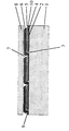
- the figure shows a schematical cross-section of an embodiment of the battery.
- the nanoporous photoelectrodes 4 are applied on a transparent conducting substrate 1, as in the original version of the dye-sensitized solar cell [Journal of the American Chemical Society, vol. 115 (1993) pp. 6382-6390], each on a predetermined area of the conducting coating 2. These areas form parallel strips of the required width for each solar cell separated by narrow insulating lines 3, where the conducting coating 2 of the substrate 1 has been removed.
- the photoelectrodes 4 are applied in such a way that each extends slightly over one edge of the corresponding conducting coating 2, while leaving bare the opposite edge.
- the photoelectrodes 4 are then covered with a porous layer of an electrical insulator 5.
- This layer is required to prevent short-circuiting in cases where the material of the counterelectrodes 6 would form ohmic contact with the photoelectrodes 4.
- the insulating layers 5 may at the same time act as a diffuse reflector that reflects light which has not yet been absorbed back into the photoelectrodes 4.
- Porous counterelectrodes 6 of any convenient electronically conducting material are now applied over the bare edge of each conducting strip 2 and the adjacent photoelectrode 4, thereby connecting the solar cells in series.
- the gaps 7 between the counterelectrodes 6 may be filled with a nonporous insulator to prevent electrical shunting through the electrolyte.
- the coatings 4 to 6 may be heat treated at any stage in order to remove undesired additives and make good electrical contacts by sintering.
- the sensitizing dye is then adsorbed through the porous counterelectrodes 6 and insulating layers 5 onto the nanoporous photoelectrodes 4. Finally the pores of layers 4 to 6 are filled with the electrolyte.
- the solar cell module is sealed by a top-cover 8, to prevent evaporation of the electrolyte and intrusion of humidity or oxygen.
- the top-cover 8 may at the same time serve to fill the gaps 7 between the counterelectrodes 6. Contacts are made at the first counterelectrode 9 and the last photoelectrode 10 of the series-connection.
- This new design of the dye-sensitized solar cell has the following advantages:
- the transparent conducting layer 2 e.g. fluorine doped tin oxide, tin doped indium oxide
- the insulating substrate 1 e.g. glass, plastic
- the transparent conducting layer 2 is scratched, etched or laser scribed in parallel lines 3 of the required separation (about 1 cm) in order to remove the conducting coating 2, thereby defining the area of each cell.
- a dispersion of nanocrystalline semiconductor powder e.g. titanium dioxide
- is applied e.g. by gravure printing or screen printing through a mask of appropriate geometry
- the photoelectrodes 4 (ca. 10 ⁇ m thick), each extending slightly over one edge of the corresponding conducting coating 2, while leaving bare the opposite edge.
- the photoelectrodes 4 may also be deposited over the whole surface first, e. g. by doctor blading, printing or spraying, and separated into parallel stripes subsequently, e. g. by mechanical, airjet, waterjet or laser scribing. This patterning may also be carried out after deposition of the insulating layers 5, by removing simultaneously the layers 4 and 5 at the required places.
- a dispersion of an insulator powder (e.g. glass or ceramics, such as aluminum oxide, silicon dioxide, titanium dioxide, zirconium dioxide) is now applied over the photoelectrodes 4 to create the porous insulating layers 5 (about 10 ⁇ m thick).
- an insulator powder e.g. glass or ceramics, such as aluminum oxide, silicon dioxide, titanium dioxide, zirconium dioxide
- the insulating layers 5 should contain particles of high refractive index (e.g. the rutile modification of titanium dioxide) and the appropriate size for strong light scattering (about 0,3 ⁇ m diameter in case of rutile).
- a binder that sinters at the temperature of heat treatment (below 550°C) may be required for the formation of well coherent and adherent layers 5.
- the binder may at the same time serve as insulator between the particles.
- the layers 5 may be obtained from a dispersion of rutile powder with a mean particle size around 0.3 ⁇ m and about 10% of its weight nanocrystalline zirconium dioxide powder with a particle size below 20 nm, which sinters on heat treatment below 550°C and forms a well insulating binder between the rutile particles.
- the rutile particles may be coated with a thin (several nanometer thick) film of an insulator (a low melting glass, silicon dioxide, aluminum dioxide, boron oxide, zirconium dioxide or a combination of these), which sinters on heat treatment below 550°C.
- the patterning of the insulating layers 5 may be achieved as described for the photoelectrodes 4 by techniques such as gravure printing or screen printing, or by mechanical, airjet, waterjet or laser scribing.
- a dispersion of a metal powder e.g. a platinum group metal, titanium, tungsten, molybdenum, chromium), graphite powder, carbon black, a conducting ceramic powder (e.g. fluorine doped tin oxide or tin doped indium oxide), optionally with a catalytic deposit of a platinum group metal, or a conducting polymer (e.g. polyaniline, polypyrrole, polythiophene) is applied for the counterelectrodes 6 (up to several 10 ⁇ m thick, depending on the required conductivity).
- a metal powder e.g. a platinum group metal, titanium, tungsten, molybdenum, chromium
- graphite powder e.g. fluorine doped tin oxide or tin doped indium oxide
- a conducting polymer e.g. polyaniline, polypyrrole, polythiophene
- Graphite powder has proven a good choice, because it combines sufficient conductivity and heat resistance as well as corrosion resistance and electrocatalytic activity with respect to the redox electrolyte.
- Graphite powder consists of platelike crystals which, on deposition from a liquid dispersion and drying, will preferentially align in the plane of the counterelectrodes 6, resulting in a high conductivity in this plane.
- the catalytic activity of the counterelectrodes 6 for reduction of the redox electrolyte as well as their conductivity may be considerably enhanced by adding about 20% of carbon black to the dispersion of graphite powder.
- the enhanced catalytic activity is due to the very high surface area of carbon black, while the improved conductivity results from the partial filling of large pores between the graphite flakes with smaller carbon black aggregates.
- photoelectrodes 4 patterning of the counterelectrodes 6 may be achieved by techniques such as gravure printing or screen printing through an appropriate mask or by mechanical, airjet, waterjet or laser scribing.
- the gaps 7 may be filled with a nonporous insulator (e.g. silicone rubber, a low melting glass frit or an organic polymer) to insulate adjacent counterelectrodes 6 from each other.
- a nonporous insulator e.g. silicone rubber, a low melting glass frit or an organic polymer
- Such an insulation is not necessary if just the pores of the coatings 4 to 6 are filled with electrolyte by capillary action later, such that the gaps 7 remain filled with air, nitrogen or another gas.
- the coatings 4 to 6 are heat treated at any stage to remove solvents and other undesired additives and to improve their mechanical strength and electrical properties by sintering.
- the coated substrate 1 is dipped into a dye solution to sensitize the photoelectrodes 4. After drying electrolyte is admitted in order to fill the pores of layers 4 to 6 by capillary action.
- the module is encapsulated with a top-cover 8 (e.g. glass, organic polymer, anodized aluminum, lacquer or any other insulator).
- the top-cover 8 may also, if necessary, serve to fill the gaps 7 between the counterelectrodes 6. Electrical contacts are made at the first counterelectrode 9 and the last photoelectrode 10 of the series-connected module.
Landscapes
- Engineering & Computer Science (AREA)
- Power Engineering (AREA)
- Microelectronics & Electronic Packaging (AREA)
- Chemical & Material Sciences (AREA)
- Chemical Kinetics & Catalysis (AREA)
- Electrochemistry (AREA)
- Photovoltaic Devices (AREA)
- Hybrid Cells (AREA)
Claims (20)
- Batterie aus photovoltaischen Zellen, die aus einer monolithischen Baugruppe aus mehreren in Reihe geschalteten photovoltaischen Elementen besteht, die als parallele, längliche Streifen auf einem gemeinsamen, elektrisch isolierenden transparenten Substrat (1) angeordnet sind, wobei jedes Element aus einer farbstoffsensibilisierten Photoanode, die aus einer porösen Schicht (4) aus einem polykristallinen Halbleiter hergestellt ist, einer Gegenelektrode, die aus einer porösen Schicht (6) aus einem elektrisch leitenden Material hergestellt ist und von der Photoanode durch eine dazwischenliegende poröse Schicht (5) eines elektrisch isolierenden Materials getrennt ist, wobei die Poren der Schichten (4, 5, 6) mindestens teilweise mit einem elektronenübertragenden Elektrolyten gefüllt sind, und einer dazwischenliegenden Schicht (2) aus einem transparenten, elektrisch leitenden Material, die zwischen dem Substrat (1) und der die Photoanode jedes Elements darstellenden Schicht (4) angeordnet ist, besteht, wobei die jeweiligen elektrisch leitenden dazwischenliegenden Schichten (2) zweier benachbarter Elemente voneinander durch eine durchgehende längliche Lücke (3) voneinander getrennt sind und die die Gegenelektrode des ersten Elements der Reihe darstellende Schicht (6) elektrisch mit einem ersten Anschluß (9) der Batterie verbunden ist, während die Schichten (6) der Gegenelektroden der anderen Elemente über die Lücke (3) elektrisch mit der dazwischenliegenden, elektrisch leitenden Schicht (2) eines benachbarten Elements verbunden ist, wobei sie voneinander elektrisch isoliert sind und die elektrisch leitende, dazwischenliegende Schicht (2) des letzten Elements der Reihe elektrisch mit einem zweiten Anschluß (10) der Batterie verbunden ist und die Baugruppe mit einer elektrisch isolierenden, flüssigkeitsdichten Abdeckung (8) abgedeckt ist.
- Batterie nach Anspruch 1, dadurch gekennzeichnet, daß die dazwischenliegende poröse Schicht (5) aus elektrisch isolierendem Material aus feinen Teilchen eines Glas- oder Keramikmaterials hergestellt ist.
- Batterie nach Anspruch 2, dadurch gekennzeichnet, daß das Material aus mindestens einem der folgenden Metalloxide besteht: Aluminiumoxid, Siliciumdioxid, Titandioxid und Zirconiumdioxid.
- Batterie nach Anspruch 2 oder 3, dadurch gekennzeichnet, daß die dazwischenliegende poröse Schicht (5) wenigstens teilweise aus mindestens einem Material mit einem hohen Brechungsindex in Form von Teilchen mit einer Größe hergestellt ist, die geeignet ist, ihnen stark lichtstreuende Eigenschaften zu geben.
- Batterie nach Anspruch 4, dadurch gekennzeichnet, daß das Material Titandioxid in Form von Rutil ist, wobei die Größe der Teilchen in der Größenordnung von 0,3 Mikrometern liegt.
- Batterie nach Anspruch 4 oder 5, dadurch gekennzeichnet, daß die dazwischenliegende poröse Schicht (5) aus einem Gemisch einer größeren Menge des Materials mit hohem Brechungsindex mit einer kleineren Menge eines elektrisch isolierenden Materials in Form von Teilchen mit einer Größe, die geeignet ist, ihnen die Eigenschaft zu geben, bei einer Temperatur unter 550°C zu sintern, besteht.
- Batterie nach Anspruch 6, dadurch gekennzeichnet, daß das elektrisch isolierende Material aus einem niedrigschmelzenden Glas oder mindestens einem der folgenden Metalloxide gewählt ist: Siliciumdioxid, Aluminiumdioxid, Bordioxid, Zirconiumdioxid oder einer Kombination mindestens zweier dieser Oxide.
- Batterie nach Anspruch 4 oder 5, dadurch gekennzeichnet, daß mindestens einige der Teilchen aus Material mit hohem Brechungsindex mit einem Film aus einem elektrisch isolierenden Material beschichtet sind, wobei der Film die Eigenschaft aufweist, bei einer Temperatur unter 550°C zu sintern.
- Batterie nach Anspruch 1, dadurch gekennzeichnet, daß die poröse Schicht (6) aus elektrisch leitendem Material aus einem Material hergestellt ist, das aus mindestens einem Metallpulver, mindestens einem elektrisch leitenden Keramikpulver, pulverförmigem Graphit, pulverförmigem Ruß, mindestens einem elektrisch leitenden organischen Polymer und Mischungen davon gewählt ist.
- Batterie nach Anspruch 9, dadurch gekennzeichnet, daß das Metall aus einem Metall der Platingruppe oder mindestens einem der folgenden Metalle gewählt ist: Titan, Wolfram, Molybdän und Chrom, wobei das elektrisch leitende Keramikmetall aus mit Fluor oder Antimon dotiertem Zinnoxid, mit Zinn dotiertem Indiumoxid gewählt ist und das elektrisch leitende organische Polymer ein Polymer auf der Basis von Polyanilin, Polypyrrol oder Polythiophen ist, wobei eine katalytische Abscheidung eines Metalls aus der Platingruppe mindestens die elektrochemisch aktive Oberfläche der von der porösen Schicht (6) gebildeten Gegenelektrode bedeckt.
- Batterie nach Anspruch 10, dadurch gekennzeichnet, daß die poröse Schicht (6) aus elektrisch leitendem Material aus einem Gemisch aus pulverförmigem Graphit, Ruß und mindestens einem Bindemittelmaterial in Form von Teilchen mit einer Größe, die sich eignet, ihnen die Eigenschaft zu geben, bei einer Temperatur unter 550°C zu sintern, hergestellt ist.
- Batterie nach Anspruch 11, dadurch gekennzeichnet, daß das Bindemittelmaterial Titandioxid mit einer Teilchengröße von unter 20 Nanometern ist.
- Batterie nach Anspruch 11 oder 12, dadurch gekennzeichnet, daß die poröse Schicht (6) aus etwa 65 Gew.-% Graphitpulver, 20 Gew.-% Ruß und 15 Gew.-% Titandioxid hergestellt ist.
- Verfahren zur Herstellung einer Batterie aus photovoltaischen Zellen nach Anspruch 1, das die folgenden Schritte umfaßt:a) Ausbilden mehrerer paralleler Streifen (2) aus einem transparenten, elektrisch leitenden Material auf der Oberfläche eines elektrisch isolierenden, transparenten Substrats (1), wobei die Streifen (2) voneinander durch eine durchgehende längliche Lücke (3) mit freier Oberfläche von Substrat (1) getrennt sind;b) Abdecken jedes der Streifen (2) mit einer porösen Schicht (4) aus einem polykristallinen Halbleiter;c) Abdecken der porösen Schicht (4) mit einer porösen Schicht (5) aus einem isolierenden Material, wobei die drei oben angegebenen Schritte a), b) und c) so durchgeführt werden, daß die porösen Schichten (4) und (5) den freiliegenden Bereich der Oberfläche des Substrats (1) in der länglichen Lücke (3) entlang einem Rand des Streifens (2) aus elektrisch leitendem Material abdecken und dabei mindestens einen Teil der Oberfläche des Streifens (2) entlang dem gegenüberliegenden Rand freilassen;d) Abdecken der porösen Schicht (5) aus isolierendem Material mit einer porösen Schicht (6) aus elektrisch leitendem Material, so daß letztere Schicht (6) die erstere Schicht (5) über ihrem, die Lücke (3) abdeckenden Teil überlappt und den freien Teil der Oberfläche des benachbarten Streifens (2) aus elektrisch leitendem Material kontaktiert und dabei an dem gegenüberliegenden Rand eine Lücke (7) läßt, wodurch eine Baugruppe aus mehreren in Reihe geschalteten Elementen gebildet wird;e) Kontaktieren der Baugruppe mit einer flüssigen Lösung aus einem Farbstoffsensibilisierer, so daß diese Lösung in die aus Halbleiter bestehende poröse Schicht (4) jedes Elements durch die poröse Schicht (6) aus elektrisch leitendem Material und die poröse Schicht (5) aus elektrisch isolierendem Material hindurch eingeführt wird;f) Verdampfen des Lösungsmittels der Lösung aus Farbstoffsensibilisierer, wobei der Farbstoff auf der Schicht (4) aus Halbleiter adsorbiert bleibt;g) Kontaktieren der Baugruppe mit einem flüssigen Elektrolyten, so daß dieser Elektrolyt die Poren der porösen Schichten (6, 5 und 4) füllt; undh) Ausbilden einer elektrischen ersten und zweiten Verbindung (9, 10) mit den Batterieanschlüssen, wobei die erste Verbindung (9) elektrisch mit der porösen Schicht (6) aus leitendem Material des ersten Elements der Batterie und die zweite Verbindung (10) elektrisch mit dem Streifen (2) aus elektrisch leitendem Material des letzten Elements verbunden ist, und Abdekken der auf diese Weise erhaltenen Baugruppe mit einer elektrisch isolierenden, flüssigkeitsdichten Abdeckung (8).
- Verfahren nach Anspruch 14, dadurch gekennzeichnet, daß die Schritte e), f) und g) miteinander verknüpft werden, indem in einem flüssigen Elektrolyten eine Lösung aus einem Farbstoffsensibilisierer verwendet wird.
- Verfahren nach Anspruch 14 oder 15, dadurch gekennzeichnet, daß es weiterhin folgenden Schritt umfaßt:i) elektrisches Isolieren der porösen Schichten (6) aus elektrisch leitendem Material aller Elemente voneinander durch Füllen der diese Schichten (6) trennenden Lücken (7) mit einem flüssigkeitsdichten isolierenden Material, wobei Schritt i) wahlweise mit dem letzten Vorgang von Schritt h) verknüpft wird.
- Verfahren nach Anspruch 14 oder 15, dadurch gekennzeichnet, daß der Schritt g) des Kontaktierens der Baugruppe mit einem flüssigen Elektrolyten derart durchgeführt wird, daß die Innenhohlräume der porösen Schichten (4, 5, 6) durch Kapillarität mit Elektrolyt gefüllt werden und daß in den Lücken (7), die die die Gegenelektrode bildenden porösen Schichten (6) trennen, ein isolierendes Gas wie beispielsweise Luft oder Stickstoff zurückbleibt.
- Verfahren nach Anspruch 14 oder 15, dadurch gekennzeichnet, daß die Schritte b), c) und d) durch geeignete Druckverfahren durchgeführt werden, um die porösen Schichten (4, 5 und 6) aus Halbleiter, isolierendem Material bzw. elektrisch leitendem Material in dem erforderlichen Muster aus parallelen Streifen auf dem Substrat (1) abzuscheiden.
- Verfahren nach Anspruch 14 oder 15, dadurch gekennzeichnet, daß die Schritte a), b) c) und d) durchgeführt werden, indem zunächst eine Schicht (2) aus transparentem, elektrisch leitendem Material auf die ganze Oberfläche des Substrats (1) aufgetragen wird, dann zum Ausbilden der Lücken (3) diese Schicht (2) an den entsprechenden Stellen entfernt wird, dann die porösen Schichten (4 und 5) aus Halbleiter bzw. isolierendem Material über die ganze Oberfläche des derart beschichteten Substrats (1) aufgetragen werden, dann zum Freilegen eines Rands jedes Streifens (2) aus transparentem, elektrisch leitenden Material diese Schichten (4 und 5) an den entsprechenden Stellen entfernt werden, dann auf die gesamte Oberfläche des derart beschichteten Substrats eine Schicht (6) aus porösem, elektrisch leitendem Material aufgetragen wird, dann zum Ausbilden der Lücken (7) diese Schicht (6), wahlweise zusammen mit den darunterliegenden porösen Schichten (4 und 5) an den entsprechenden Stellen entfernt wird.
- Verfahren nach Anspruch 18 oder 19, dadurch gekennzeichnet, daß die länglichen Lücken (3) und die porösen Schichten (4, 5, 6) in einem durchgehenden Verfahren gefertigt werden, und zwar nacheinander durch Strukturieren der Schicht (2) aus transparentem, elektrisch leitenden Material und Abscheiden, Strukturieren und Wärmbehandlung der die Photoanoden darstellenden Schicht (4), der Schicht (5) aus isolierendem Material und der Schicht (6) aus elektrisch leitendem Material auf dem Substrat (1) bei gleichzeitigem ständigem Transport von letzterem entlang der Länge der länglichen Lücken (3) durch mehrere Arbeitsstationen.
Applications Claiming Priority (1)
| Application Number | Priority Date | Filing Date | Title |
|---|---|---|---|
| PCT/IB1995/000936 WO1997016838A1 (en) | 1995-10-31 | 1995-10-31 | A battery of photovoltaic cells and process for manufacturing the same |
Publications (2)
| Publication Number | Publication Date |
|---|---|
| EP0858669A1 EP0858669A1 (de) | 1998-08-19 |
| EP0858669B1 true EP0858669B1 (de) | 1999-11-03 |
Family
ID=11004384
Family Applications (1)
| Application Number | Title | Priority Date | Filing Date |
|---|---|---|---|
| EP95934259A Expired - Lifetime EP0858669B1 (de) | 1995-10-31 | 1995-10-31 | Batterie-anordnung von fotovoltaischen zellen und herstellungsverfahren |
Country Status (6)
| Country | Link |
|---|---|
| US (1) | US6069313A (de) |
| EP (1) | EP0858669B1 (de) |
| JP (1) | JP4087445B2 (de) |
| AU (1) | AU728725B2 (de) |
| DE (1) | DE69513203T2 (de) |
| WO (1) | WO1997016838A1 (de) |
Cited By (1)
| Publication number | Priority date | Publication date | Assignee | Title |
|---|---|---|---|---|
| DE10249246B4 (de) * | 2002-10-23 | 2013-01-17 | Fraunhofer-Gesellschaft zur Förderung der angewandten Forschung e.V. | Farbstoffsensibilisierte photovoltaische Zelle, ein Verfahren zur Herstellung dieser photovoltaischen Zellen sowie deren Verwendung |
Families Citing this family (157)
| Publication number | Priority date | Publication date | Assignee | Title |
|---|---|---|---|---|
| AUPP931799A0 (en) * | 1999-03-18 | 1999-04-15 | Sustainable Technologies Australia Limited | Methods to implement interconnects in multi-cell regenerative photovoltaic photoelectrochemical devices |
| AUPP953999A0 (en) * | 1999-03-30 | 1999-04-29 | Sustainable Technologies Australia Limited | Methods to manufacture single cell and multi-cell regenerative photoelectrochemical devices |
| JP4414036B2 (ja) * | 1999-12-27 | 2010-02-10 | シャープ株式会社 | 色素増感型太陽電池の作製方法 |
| US6305073B1 (en) | 1999-12-29 | 2001-10-23 | Gm Nameplate, Inc. | One-sided electrode arrangement on an intermediate spacer for a touchscreen |
| US6949400B2 (en) * | 2002-01-25 | 2005-09-27 | Konarka Technologies, Inc. | Ultrasonic slitting of photovoltaic cells and modules |
| US7205473B2 (en) * | 2002-01-25 | 2007-04-17 | Konarka Technologies, Inc. | Photovoltaic powered multimedia greeting cards and smart cards |
| US20030192584A1 (en) * | 2002-01-25 | 2003-10-16 | Konarka Technologies, Inc. | Flexible photovoltaic cells and modules formed using foils |
| US20050284513A1 (en) * | 2002-08-08 | 2005-12-29 | Christoph Brabec | Chip card comprising an integrated energy converter |
| US6900382B2 (en) | 2002-01-25 | 2005-05-31 | Konarka Technologies, Inc. | Gel electrolytes for dye sensitized solar cells |
| US20030192585A1 (en) * | 2002-01-25 | 2003-10-16 | Konarka Technologies, Inc. | Photovoltaic cells incorporating rigid substrates |
| US6913713B2 (en) | 2002-01-25 | 2005-07-05 | Konarka Technologies, Inc. | Photovoltaic fibers |
| US7186911B2 (en) * | 2002-01-25 | 2007-03-06 | Konarka Technologies, Inc. | Methods of scoring for fabricating interconnected photovoltaic cells |
| US6706963B2 (en) * | 2002-01-25 | 2004-03-16 | Konarka Technologies, Inc. | Photovoltaic cell interconnection |
| US7414188B2 (en) * | 2002-01-25 | 2008-08-19 | Konarka Technologies, Inc. | Co-sensitizers for dye sensitized solar cells |
| US6919119B2 (en) * | 2000-05-30 | 2005-07-19 | The Penn State Research Foundation | Electronic and opto-electronic devices fabricated from nanostructured high surface to volume ratio thin films |
| SE521683C2 (sv) | 2000-06-14 | 2003-11-25 | Ivf Industriforskning Och Utve | Metod för tillverkning av förseglade monolitiska elektrokemiska system och förseglat monolitiskt elektrokemiskt system |
| AUPR174800A0 (en) * | 2000-11-29 | 2000-12-21 | Australian National University, The | Semiconductor processing |
| KR20030063469A (ko) * | 2000-12-26 | 2003-07-28 | (주)하야시바라 생물화학연구소 | 태양전지 |
| DE10120579C2 (de) * | 2001-04-26 | 2003-06-26 | Siemens Ag | Hochsensibler Feuchteindikator für Dünnfilmtechnologie |
| WO2003059570A1 (en) * | 2002-01-04 | 2003-07-24 | G.T. Equipment Technologies Inc. | Solar cell stringing machine |
| WO2003065472A2 (en) * | 2002-01-25 | 2003-08-07 | Konarka Technologies, Inc. | Structures and materials for dye sensitized solar cells |
| WO2003065393A2 (en) * | 2002-01-25 | 2003-08-07 | Konarka Technologies, Inc. | Displays with integrated photovoltaic cells |
| JP4644427B2 (ja) * | 2002-01-25 | 2011-03-02 | コナルカ テクノロジーズ インコーポレイテッド | 太陽電池に用いるための感光性ナノ粒子を低温で相互に結合させる方法及び該方法において用いられるポリマー連結剤溶液 |
| JP4392741B2 (ja) * | 2002-04-17 | 2010-01-06 | 日揮触媒化成株式会社 | 光電気セル |
| WO2004036683A1 (ja) | 2002-10-15 | 2004-04-29 | Sharp Kabushiki Kaisha | 色素増感型太陽電池及び色素増感型太陽電池モジュール |
| JP4161688B2 (ja) * | 2002-11-18 | 2008-10-08 | アイシン精機株式会社 | 湿式太陽電池 |
| US9682425B2 (en) | 2009-12-08 | 2017-06-20 | Baker Hughes Incorporated | Coated metallic powder and method of making the same |
| US9101978B2 (en) | 2002-12-08 | 2015-08-11 | Baker Hughes Incorporated | Nanomatrix powder metal compact |
| US8297364B2 (en) | 2009-12-08 | 2012-10-30 | Baker Hughes Incorporated | Telescopic unit with dissolvable barrier |
| US8327931B2 (en) * | 2009-12-08 | 2012-12-11 | Baker Hughes Incorporated | Multi-component disappearing tripping ball and method for making the same |
| US9109429B2 (en) | 2002-12-08 | 2015-08-18 | Baker Hughes Incorporated | Engineered powder compact composite material |
| US8403037B2 (en) * | 2009-12-08 | 2013-03-26 | Baker Hughes Incorporated | Dissolvable tool and method |
| US9079246B2 (en) | 2009-12-08 | 2015-07-14 | Baker Hughes Incorporated | Method of making a nanomatrix powder metal compact |
| US7078613B2 (en) * | 2002-12-11 | 2006-07-18 | General Electric Company | Structured micro-channel semiconductor electrode for photovoltaic cells |
| IL153895A (en) * | 2003-01-12 | 2013-01-31 | Orion Solar Systems Ltd | Solar cell device |
| US8586861B2 (en) * | 2003-01-12 | 2013-11-19 | 3Gsolar Photovoltaics Ltd. | Solar cell device |
| US7170001B2 (en) * | 2003-06-26 | 2007-01-30 | Advent Solar, Inc. | Fabrication of back-contacted silicon solar cells using thermomigration to create conductive vias |
| US7649141B2 (en) * | 2003-06-30 | 2010-01-19 | Advent Solar, Inc. | Emitter wrap-through back contact solar cells on thin silicon wafers |
| JP2005158470A (ja) * | 2003-11-25 | 2005-06-16 | Ngk Spark Plug Co Ltd | 色素増感型太陽電池 |
| JP3717506B2 (ja) | 2004-01-20 | 2005-11-16 | シャープ株式会社 | 色素増感型太陽電池モジュール |
| US7335555B2 (en) * | 2004-02-05 | 2008-02-26 | Advent Solar, Inc. | Buried-contact solar cells with self-doping contacts |
| US20050172996A1 (en) * | 2004-02-05 | 2005-08-11 | Advent Solar, Inc. | Contact fabrication of emitter wrap-through back contact silicon solar cells |
| US20060060238A1 (en) * | 2004-02-05 | 2006-03-23 | Advent Solar, Inc. | Process and fabrication methods for emitter wrap through back contact solar cells |
| US7144751B2 (en) * | 2004-02-05 | 2006-12-05 | Advent Solar, Inc. | Back-contact solar cells and methods for fabrication |
| WO2005083730A1 (en) * | 2004-02-19 | 2005-09-09 | Konarka Technologies, Inc. | Photovoltaic cell with spacers |
| US7781672B2 (en) * | 2004-06-01 | 2010-08-24 | Konarka Technologies, Inc. | Photovoltaic module architecture |
| JP4063802B2 (ja) * | 2004-08-04 | 2008-03-19 | シャープ株式会社 | 光電極 |
| AU2005270739B2 (en) * | 2004-08-11 | 2009-12-24 | Dyesol Ltd | Photoelectrochemical Photovoltaic Panel and method to manufacture thereof |
| KR101131834B1 (ko) * | 2004-08-11 | 2012-03-30 | 다이솔 엘티디 | 광전기화학 광전지 패널 및 그의 제조 방법 |
| US8309843B2 (en) * | 2004-08-19 | 2012-11-13 | Banpil Photonics, Inc. | Photovoltaic cells based on nanoscale structures |
| EP1917558B1 (de) * | 2005-08-22 | 2018-07-25 | Merck Patent GmbH | Anzeigen mit integrierten photovoltaischen zellen |
| US20070079867A1 (en) * | 2005-10-12 | 2007-04-12 | Kethinni Chittibabu | Photovoltaic fibers |
| US8314327B2 (en) * | 2005-11-06 | 2012-11-20 | Banpil Photonics, Inc. | Photovoltaic cells based on nano or micro-scale structures |
| GB2432723B (en) * | 2005-11-25 | 2010-12-08 | Seiko Epson Corp | Electrochemical cell and method of manufacture |
| GB2432721B (en) * | 2005-11-25 | 2011-06-22 | Seiko Epson Corp | Electrochemical cell structure and method of fabrication |
| GB2432722A (en) * | 2005-11-25 | 2007-05-30 | Seiko Epson Corp | Electrochemical cell and method of manufacture |
| US20070125419A1 (en) * | 2005-12-01 | 2007-06-07 | Gui John Y | Dye sensitized solar cells having blocking layers and methods of manufacturing the same |
| JP4523549B2 (ja) | 2006-01-18 | 2010-08-11 | シャープ株式会社 | 色素増感太陽電池および色素増感太陽電池モジュール |
| TWI346406B (en) * | 2006-02-16 | 2011-08-01 | Lg Chemical Ltd | Lithium secondary battery with enhanced heat-resistance |
| EP1840916A1 (de) * | 2006-03-27 | 2007-10-03 | IVF Industriforskning och Utveckling AB | Versiegeltes monolithisches photo-elektrochemisches System und Verfahren zur Herstellung versiegelter monolithischer photo-elektrochemischer Systeme |
| WO2008004556A1 (fr) | 2006-07-06 | 2008-01-10 | Sharp Kabushiki Kaisha | Module de cellule solaire sensible aux colorants et procédé de fabrication correspondant |
| US8933328B2 (en) | 2006-07-06 | 2015-01-13 | Sharp Kabushiki Kaisha | Dye-sensitized solar cell module and method of producing the same |
| CA2568136C (en) * | 2006-11-30 | 2008-07-29 | Tenxc Wireless Inc. | Butler matrix implementation |
| WO2008080160A1 (en) * | 2006-12-22 | 2008-07-03 | Advent Solar, Inc. | Interconnect technologies for back contact solar cells and modules |
| EP1936644A3 (de) * | 2006-12-22 | 2011-01-05 | Sony Deutschland Gmbh | Photovoltaische Zelle |
| WO2009053979A2 (en) * | 2007-10-24 | 2009-04-30 | 3Gsolar Ltd. | Monolithic dye cell assembly having reduced ion migration in intercell seals |
| WO2009001343A2 (en) * | 2007-06-24 | 2008-12-31 | 3Gsolar Ltd. | Dry cell having a sintered cathode layer |
| WO2008149811A1 (ja) * | 2007-06-06 | 2008-12-11 | Fujikura Ltd. | 色素増感太陽電池モジュールおよびその製造方法 |
| JP4488034B2 (ja) * | 2007-06-29 | 2010-06-23 | 株式会社日立製作所 | 色素増感太陽電池 |
| JP2009110796A (ja) * | 2007-10-30 | 2009-05-21 | Sony Corp | 色素増感光電変換素子モジュールおよびその製造方法ならびに電子機器 |
| US20090126786A1 (en) * | 2007-11-13 | 2009-05-21 | Advent Solar, Inc. | Selective Emitter and Texture Processes for Back Contact Solar Cells |
| KR20090051597A (ko) * | 2007-11-19 | 2009-05-22 | 한국전자통신연구원 | 전도성 섬유 전극을 사용하는 염료감응 태양전지 |
| BRPI0819601A2 (pt) * | 2007-11-27 | 2016-04-05 | 3Gsolar Ltd | célula fotovoltaica para converter uma fonte de luz em eletricidade, método de produção de uma célula fotovoltaica para converter uma fonte de luz em eletricidade. |
| JP5377327B2 (ja) | 2007-12-12 | 2013-12-25 | シャープ株式会社 | 光増感太陽電池モジュールおよびその製造方法 |
| JP2009146625A (ja) * | 2007-12-12 | 2009-07-02 | Sony Corp | 色素増感光電変換素子モジュールおよびその製造方法ならびに光電変換素子モジュールおよびその製造方法ならびに電子機器 |
| GB2456166B (en) * | 2008-01-04 | 2012-01-25 | Pv Systems Ltd | A photovoltaic panel |
| EP2085986A1 (de) | 2008-01-30 | 2009-08-05 | Swerea IVF AB | Versiegeltes monolithisches, elektrochemisches System |
| JP5351553B2 (ja) * | 2008-04-28 | 2013-11-27 | 株式会社フジクラ | 光電変換素子モジュール |
| KR20110008284A (ko) * | 2008-04-29 | 2011-01-26 | 어플라이드 머티어리얼스, 인코포레이티드 | 모놀리식 모듈 어셈블리 기술들을 이용하여 제조된 광전지 모듈들 |
| JP5273709B2 (ja) | 2008-07-02 | 2013-08-28 | シャープ株式会社 | 色素増感太陽電池、その製造方法および色素増感太陽電池モジュール |
| US20100006148A1 (en) * | 2008-07-08 | 2010-01-14 | Honeywell International Inc. | Solar cell with porous insulating layer |
| KR20110083607A (ko) * | 2008-08-29 | 2011-07-20 | 칠룸 베타일리공스 게젤샤프트 엠베하 운트 코. 파텐테 Ii 카게 | 태양광 흡수체용 층 시스템 |
| TW201013947A (en) * | 2008-09-23 | 2010-04-01 | Tripod Technology Corp | Electrochemical device and method of fabricating the same |
| JPWO2010044445A1 (ja) * | 2008-10-17 | 2012-03-15 | シャープ株式会社 | 色素増感太陽電池および色素増感太陽電池モジュール |
| WO2012037445A2 (en) | 2010-09-17 | 2012-03-22 | Drexel University | Novel applications for alliform carbon |
| EP2421084B1 (de) | 2009-04-15 | 2014-03-19 | Sharp Kabushiki Kaisha | Farbstoffsensibilisierte solarzelle und farbstoffsensibilisiertes solarzellenmodul |
| JP4683396B2 (ja) * | 2009-04-30 | 2011-05-18 | シャープ株式会社 | 多孔質電極、色素増感太陽電池、および色素増感太陽電池モジュール |
| JP2010278405A (ja) * | 2009-06-01 | 2010-12-09 | Smart Solar International Inc | 太陽光発電システム及び太陽光発電装置 |
| EP2312641A1 (de) * | 2009-10-13 | 2011-04-20 | Ecole Polytechnique Fédérale de Lausanne (EPFL) | Vorrichtung mit elektrischen Kontakten und deren Herstellungsverfahren |
| US20120211048A1 (en) | 2009-11-02 | 2012-08-23 | Norio Murofushi | Wet solar cell and wet solar cell module |
| US20110108102A1 (en) * | 2009-11-06 | 2011-05-12 | Honeywell International Inc. | Solar cell with enhanced efficiency |
| KR101108182B1 (ko) * | 2009-12-01 | 2012-01-31 | 삼성에스디아이 주식회사 | 염료감응 태양전지 |
| US10240419B2 (en) | 2009-12-08 | 2019-03-26 | Baker Hughes, A Ge Company, Llc | Downhole flow inhibition tool and method of unplugging a seat |
| US8425651B2 (en) | 2010-07-30 | 2013-04-23 | Baker Hughes Incorporated | Nanomatrix metal composite |
| US8573295B2 (en) | 2010-11-16 | 2013-11-05 | Baker Hughes Incorporated | Plug and method of unplugging a seat |
| US8528633B2 (en) | 2009-12-08 | 2013-09-10 | Baker Hughes Incorporated | Dissolvable tool and method |
| US9127515B2 (en) | 2010-10-27 | 2015-09-08 | Baker Hughes Incorporated | Nanomatrix carbon composite |
| US9227243B2 (en) | 2009-12-08 | 2016-01-05 | Baker Hughes Incorporated | Method of making a powder metal compact |
| US9243475B2 (en) | 2009-12-08 | 2016-01-26 | Baker Hughes Incorporated | Extruded powder metal compact |
| JP4761327B2 (ja) * | 2010-01-12 | 2011-08-31 | シャープ株式会社 | 湿式太陽電池および湿式太陽電池モジュール |
| JP5424259B2 (ja) | 2010-02-02 | 2014-02-26 | シャープ株式会社 | 太陽電池および太陽電池モジュール |
| US8424610B2 (en) | 2010-03-05 | 2013-04-23 | Baker Hughes Incorporated | Flow control arrangement and method |
| US9752932B2 (en) | 2010-03-10 | 2017-09-05 | Drexel University | Tunable electro-optic filter stack |
| JP4803305B2 (ja) * | 2010-03-30 | 2011-10-26 | 大日本印刷株式会社 | 色素増感型太陽電池 |
| JP5714005B2 (ja) | 2010-06-09 | 2015-05-07 | シャープ株式会社 | 湿式太陽電池および湿式太陽電池モジュール |
| US8563351B2 (en) * | 2010-06-25 | 2013-10-22 | Taiwan Semiconductor Manufacturing Co., Ltd. | Method for manufacturing photovoltaic device |
| US8776884B2 (en) | 2010-08-09 | 2014-07-15 | Baker Hughes Incorporated | Formation treatment system and method |
| JP6027008B2 (ja) * | 2010-10-10 | 2016-11-16 | ザ トラスティーズ オブ プリンストン ユニバーシテイ | 太陽電池用のグラフェン電極 |
| JP5758400B2 (ja) | 2010-10-18 | 2015-08-05 | シャープ株式会社 | 色素増感太陽電池モジュールおよびその製造方法 |
| US9090955B2 (en) | 2010-10-27 | 2015-07-28 | Baker Hughes Incorporated | Nanomatrix powder metal composite |
| WO2012070562A1 (ja) | 2010-11-24 | 2012-05-31 | シャープ株式会社 | 光電変換素子およびその製造方法 |
| JP5313278B2 (ja) * | 2011-02-28 | 2013-10-09 | シャープ株式会社 | 光電変換素子および光電変換素子モジュール |
| US8631876B2 (en) | 2011-04-28 | 2014-01-21 | Baker Hughes Incorporated | Method of making and using a functionally gradient composite tool |
| US9080098B2 (en) | 2011-04-28 | 2015-07-14 | Baker Hughes Incorporated | Functionally gradient composite article |
| JP5118233B2 (ja) | 2011-06-08 | 2013-01-16 | シャープ株式会社 | 光電変換素子および光電変換素子モジュール |
| US10916382B2 (en) | 2011-06-08 | 2021-02-09 | Sharp Kabushiki Kaisha | Photoelectric conversion element and photoelectric conversion element module |
| US9073937B2 (en) | 2011-06-16 | 2015-07-07 | Board Of Trustees Of The University Of Alabama | Organic photovoltaic-battery hybrid device |
| US9139928B2 (en) | 2011-06-17 | 2015-09-22 | Baker Hughes Incorporated | Corrodible downhole article and method of removing the article from downhole environment |
| US9707739B2 (en) | 2011-07-22 | 2017-07-18 | Baker Hughes Incorporated | Intermetallic metallic composite, method of manufacture thereof and articles comprising the same |
| US8783365B2 (en) | 2011-07-28 | 2014-07-22 | Baker Hughes Incorporated | Selective hydraulic fracturing tool and method thereof |
| US9643250B2 (en) | 2011-07-29 | 2017-05-09 | Baker Hughes Incorporated | Method of controlling the corrosion rate of alloy particles, alloy particle with controlled corrosion rate, and articles comprising the particle |
| US9833838B2 (en) | 2011-07-29 | 2017-12-05 | Baker Hughes, A Ge Company, Llc | Method of controlling the corrosion rate of alloy particles, alloy particle with controlled corrosion rate, and articles comprising the particle |
| US9057242B2 (en) | 2011-08-05 | 2015-06-16 | Baker Hughes Incorporated | Method of controlling corrosion rate in downhole article, and downhole article having controlled corrosion rate |
| US9033055B2 (en) | 2011-08-17 | 2015-05-19 | Baker Hughes Incorporated | Selectively degradable passage restriction and method |
| US9109269B2 (en) | 2011-08-30 | 2015-08-18 | Baker Hughes Incorporated | Magnesium alloy powder metal compact |
| US9090956B2 (en) | 2011-08-30 | 2015-07-28 | Baker Hughes Incorporated | Aluminum alloy powder metal compact |
| US9856547B2 (en) | 2011-08-30 | 2018-01-02 | Bakers Hughes, A Ge Company, Llc | Nanostructured powder metal compact |
| US9643144B2 (en) | 2011-09-02 | 2017-05-09 | Baker Hughes Incorporated | Method to generate and disperse nanostructures in a composite material |
| US9187990B2 (en) | 2011-09-03 | 2015-11-17 | Baker Hughes Incorporated | Method of using a degradable shaped charge and perforating gun system |
| US9347119B2 (en) | 2011-09-03 | 2016-05-24 | Baker Hughes Incorporated | Degradable high shock impedance material |
| US9133695B2 (en) | 2011-09-03 | 2015-09-15 | Baker Hughes Incorporated | Degradable shaped charge and perforating gun system |
| US9284812B2 (en) | 2011-11-21 | 2016-03-15 | Baker Hughes Incorporated | System for increasing swelling efficiency |
| US9010416B2 (en) | 2012-01-25 | 2015-04-21 | Baker Hughes Incorporated | Tubular anchoring system and a seat for use in the same |
| US9068428B2 (en) | 2012-02-13 | 2015-06-30 | Baker Hughes Incorporated | Selectively corrodible downhole article and method of use |
| SE537669C2 (sv) * | 2012-04-04 | 2015-09-29 | Exeger Sweden Ab | Färgämnessensiterad solcellsmodul med seriekopplad struktursamt sätt för framställning av solcellen |
| JPWO2013161557A1 (ja) | 2012-04-23 | 2015-12-24 | シャープ株式会社 | 光電変換素子モジュールおよびその製造方法 |
| JP2013232362A (ja) | 2012-05-01 | 2013-11-14 | Sharp Corp | 光電変換素子および光電変換モジュール |
| US9605508B2 (en) | 2012-05-08 | 2017-03-28 | Baker Hughes Incorporated | Disintegrable and conformable metallic seal, and method of making the same |
| EP2833427A4 (de) | 2012-05-09 | 2016-02-24 | Lg Chemical Ltd | Organische elektrochemische vorrichtung und verfahren zur herstellung davon |
| EP2879230A4 (de) * | 2012-07-27 | 2015-10-28 | Daicel Corp | Zusammensetzung mit einer schicht für fotoelektrische umwandlung und element für fotoelektrische umwandlung |
| WO2014017536A1 (ja) * | 2012-07-27 | 2014-01-30 | 株式会社ダイセル | 光電変換層用組成物および光電変換素子 |
| WO2014038570A1 (ja) | 2012-09-07 | 2014-03-13 | シャープ株式会社 | 光電変換素子、その製造方法、光電変換素子モジュールおよびその製造方法 |
| US10964486B2 (en) | 2013-05-17 | 2021-03-30 | Exeger Operations Ab | Dye-sensitized solar cell unit and a photovoltaic charger including the solar cell unit |
| ES2748174T3 (es) | 2013-05-17 | 2020-03-13 | Exeger Operations Ab | Una célula solar sensibilizada por colorante y un método para fabricar la célula solar |
| CN103441217B (zh) * | 2013-07-16 | 2015-11-04 | 华中科技大学 | 基于钙钛矿类吸光材料的介观太阳能电池及其制备方法 |
| US9816339B2 (en) | 2013-09-03 | 2017-11-14 | Baker Hughes, A Ge Company, Llc | Plug reception assembly and method of reducing restriction in a borehole |
| CA2936851A1 (en) | 2014-02-21 | 2015-08-27 | Terves, Inc. | Fluid activated disintegrating metal system |
| US11167343B2 (en) | 2014-02-21 | 2021-11-09 | Terves, Llc | Galvanically-active in situ formed particles for controlled rate dissolving tools |
| US10865465B2 (en) | 2017-07-27 | 2020-12-15 | Terves, Llc | Degradable metal matrix composite |
| EP2985799A1 (de) | 2014-08-11 | 2016-02-17 | Dyenamo AB | Festkörperlochleitermaterial |
| US9910026B2 (en) | 2015-01-21 | 2018-03-06 | Baker Hughes, A Ge Company, Llc | High temperature tracers for downhole detection of produced water |
| US10378303B2 (en) | 2015-03-05 | 2019-08-13 | Baker Hughes, A Ge Company, Llc | Downhole tool and method of forming the same |
| US10221637B2 (en) | 2015-08-11 | 2019-03-05 | Baker Hughes, A Ge Company, Llc | Methods of manufacturing dissolvable tools via liquid-solid state molding |
| US10016810B2 (en) | 2015-12-14 | 2018-07-10 | Baker Hughes, A Ge Company, Llc | Methods of manufacturing degradable tools using a galvanic carrier and tools manufactured thereof |
| AU2017230039B2 (en) | 2016-03-10 | 2021-09-02 | Exeger Operations Ab | A solar cell comprising grains of a doped semiconducting material and a method for manufacturing the solar cell |
| JP6104446B1 (ja) | 2016-10-07 | 2017-03-29 | 株式会社昭和 | 色素増感型太陽電池モジュール |
| DE102018132342A1 (de) * | 2018-12-14 | 2020-06-18 | Heliatek Gmbh | Stabilisierung laserstrukturierter organischer Photovoltaik |
Family Cites Families (7)
| Publication number | Priority date | Publication date | Assignee | Title |
|---|---|---|---|---|
| US4097655A (en) * | 1976-07-16 | 1978-06-27 | Optel Corporation | Photogalvanic cell using a transparent conducting electrode |
| US4754544A (en) * | 1985-01-30 | 1988-07-05 | Energy Conversion Devices, Inc. | Extremely lightweight, flexible semiconductor device arrays |
| US4968354A (en) * | 1987-11-09 | 1990-11-06 | Fuji Electric Co., Ltd. | Thin film solar cell array |
| CA2024662A1 (en) * | 1989-09-08 | 1991-03-09 | Robert Oswald | Monolithic series and parallel connected photovoltaic module |
| ES2080313T3 (es) * | 1990-04-17 | 1996-02-01 | Ecole Polytech | Celulas fotovoltaicas. |
| US5273911A (en) * | 1991-03-07 | 1993-12-28 | Mitsubishi Denki Kabushiki Kaisha | Method of producing a thin-film solar cell |
| DE4225576A1 (de) * | 1992-08-03 | 1994-02-10 | Abb Patent Gmbh | Photoelektrochemische Zelle |
-
1995
- 1995-10-31 DE DE69513203T patent/DE69513203T2/de not_active Expired - Lifetime
- 1995-10-31 WO PCT/IB1995/000936 patent/WO1997016838A1/en active IP Right Grant
- 1995-10-31 EP EP95934259A patent/EP0858669B1/de not_active Expired - Lifetime
- 1995-10-31 US US09/066,323 patent/US6069313A/en not_active Expired - Lifetime
- 1995-10-31 AU AU36719/95A patent/AU728725B2/en not_active Expired
- 1995-10-31 JP JP51717797A patent/JP4087445B2/ja not_active Expired - Lifetime
Cited By (1)
| Publication number | Priority date | Publication date | Assignee | Title |
|---|---|---|---|---|
| DE10249246B4 (de) * | 2002-10-23 | 2013-01-17 | Fraunhofer-Gesellschaft zur Förderung der angewandten Forschung e.V. | Farbstoffsensibilisierte photovoltaische Zelle, ein Verfahren zur Herstellung dieser photovoltaischen Zellen sowie deren Verwendung |
Also Published As
| Publication number | Publication date |
|---|---|
| EP0858669A1 (de) | 1998-08-19 |
| WO1997016838A1 (en) | 1997-05-09 |
| DE69513203D1 (de) | 1999-12-09 |
| US6069313A (en) | 2000-05-30 |
| AU728725B2 (en) | 2001-01-18 |
| DE69513203T2 (de) | 2000-07-20 |
| JP4087445B2 (ja) | 2008-05-21 |
| AU3671995A (en) | 1997-05-22 |
Similar Documents
| Publication | Publication Date | Title |
|---|---|---|
| EP0858669B1 (de) | Batterie-anordnung von fotovoltaischen zellen und herstellungsverfahren | |
| JPH11514787A (ja) | 光起電力セル電池及びその製造方法 | |
| US7145071B2 (en) | Dye sensitized solar cell having finger electrodes | |
| Matsui et al. | Application of an ionic liquid-based electrolyte to a 100mm× 100 mm sized dye-sensitized solar cell | |
| US20100132785A1 (en) | Dye-sensitized photoelectric conversion element module and a method of manufacturing the same, and photoelectric conversion element module and a method of manufacturing the same, and electronic apparatus | |
| EP2214249A1 (de) | Farbstoffempfindliches photoelektrisches wandlungsvorrichtungsmodul, verfahren zu seiner herstellung und elektronische vorrichtung | |
| Knödler et al. | Photoelectrochemical cells based on dye sensitized colloidal TiO2 layers | |
| WO2008139479A2 (en) | Photovoltaic cell | |
| EP0855726A1 (de) | Sonnenzelle und Verfahren für seine Herstellung | |
| JP4698028B2 (ja) | 多重セル再生型光起電光電気化学デバイスにおける導通路を設ける方法 | |
| JP2001160426A (ja) | 色素増感型太陽電池、その製造方法およびこれを用いた携帯用機器 | |
| Vesce et al. | Fabrication of spacer and catalytic layers in monolithic dye-sensitized solar cells | |
| JPH11266028A (ja) | 光電変換素子 | |
| US6652904B1 (en) | Methods to manufacture single cell and multi-cell regenerative photoelectrochemical devices | |
| US7078613B2 (en) | Structured micro-channel semiconductor electrode for photovoltaic cells | |
| DE4416247A1 (de) | Monolithische, serienverschaltete, farbstoffsensibilisierte photovoltaische Module | |
| AU3520795A (en) | Electrochemical photovoltaic cell | |
| JP2008204881A (ja) | 光電変換モジュール | |
| WO2010042170A2 (en) | Interconnection of adjacent devices | |
| JP4155431B2 (ja) | 光電変換素子 | |
| EP1543570A1 (de) | Fotovoltaische einrichtung mit einer 1,3,5-trisaminophenylbenzolverbindung | |
| WO1998036434A1 (en) | Method for the manufacture of photovoltaic cell | |
| EP2359406B1 (de) | Photovoltaische elemente | |
| JP2002353483A (ja) | 色素増感太陽電池、及びその製造方法 | |
| JP2003123855A (ja) | 光電変換素子用光電極 |
Legal Events
| Date | Code | Title | Description |
|---|---|---|---|
| PUAI | Public reference made under article 153(3) epc to a published international application that has entered the european phase |
Free format text: ORIGINAL CODE: 0009012 |
|
| 17P | Request for examination filed |
Effective date: 19980504 |
|
| AK | Designated contracting states |
Kind code of ref document: A1 Designated state(s): CH DE FR GB IT LI NL SE |
|
| GRAG | Despatch of communication of intention to grant |
Free format text: ORIGINAL CODE: EPIDOS AGRA |
|
| 17Q | First examination report despatched |
Effective date: 19990208 |
|
| GRAG | Despatch of communication of intention to grant |
Free format text: ORIGINAL CODE: EPIDOS AGRA |
|
| GRAH | Despatch of communication of intention to grant a patent |
Free format text: ORIGINAL CODE: EPIDOS IGRA |
|
| GRAH | Despatch of communication of intention to grant a patent |
Free format text: ORIGINAL CODE: EPIDOS IGRA |
|
| GRAA | (expected) grant |
Free format text: ORIGINAL CODE: 0009210 |
|
| AK | Designated contracting states |
Kind code of ref document: B1 Designated state(s): CH DE FR GB IT LI NL SE |
|
| REG | Reference to a national code |
Ref country code: CH Ref legal event code: EP |
|
| REF | Corresponds to: |
Ref document number: 69513203 Country of ref document: DE Date of ref document: 19991209 |
|
| REG | Reference to a national code |
Ref country code: CH Ref legal event code: NV Representative=s name: ABREMA AGENCE BREVETS ET MARQUES GANGUILLET & HUMP |
|
| ITF | It: translation for a ep patent filed |
Owner name: ST. DR. CAVATTONI ING. A. RAIMONDI |
|
| ET | Fr: translation filed | ||
| REG | Reference to a national code |
Ref country code: CH Ref legal event code: AEN Free format text: LE BREVET A ETE REACTIVE SELON LA DEMANDE DE POURSUITE DE LA PROCEDURE DU 11.02.2000 |
|
| PLBE | No opposition filed within time limit |
Free format text: ORIGINAL CODE: 0009261 |
|
| STAA | Information on the status of an ep patent application or granted ep patent |
Free format text: STATUS: NO OPPOSITION FILED WITHIN TIME LIMIT |
|
| 26N | No opposition filed | ||
| REG | Reference to a national code |
Ref country code: GB Ref legal event code: IF02 |
|
| PGFP | Annual fee paid to national office [announced via postgrant information from national office to epo] |
Ref country code: SE Payment date: 20141021 Year of fee payment: 20 Ref country code: CH Payment date: 20141103 Year of fee payment: 20 Ref country code: FR Payment date: 20141022 Year of fee payment: 20 Ref country code: DE Payment date: 20141022 Year of fee payment: 20 Ref country code: GB Payment date: 20141021 Year of fee payment: 20 |
|
| PGFP | Annual fee paid to national office [announced via postgrant information from national office to epo] |
Ref country code: NL Payment date: 20141021 Year of fee payment: 20 |
|
| PGFP | Annual fee paid to national office [announced via postgrant information from national office to epo] |
Ref country code: IT Payment date: 20141030 Year of fee payment: 20 |
|
| REG | Reference to a national code |
Ref country code: CH Ref legal event code: PL |
|
| REG | Reference to a national code |
Ref country code: DE Ref legal event code: R071 Ref document number: 69513203 Country of ref document: DE |
|
| REG | Reference to a national code |
Ref country code: NL Ref legal event code: MK Effective date: 20151030 |
|
| REG | Reference to a national code |
Ref country code: CH Ref legal event code: PL |
|
| REG | Reference to a national code |
Ref country code: GB Ref legal event code: PE20 Expiry date: 20151030 |
|
| PG25 | Lapsed in a contracting state [announced via postgrant information from national office to epo] |
Ref country code: GB Free format text: LAPSE BECAUSE OF EXPIRATION OF PROTECTION Effective date: 20151030 |