EP0849603A2 - Verbinder zur Prüfung von Flüssigkristallanzeigen und Verfahren zu seiner Herstellung - Google Patents
Verbinder zur Prüfung von Flüssigkristallanzeigen und Verfahren zu seiner Herstellung Download PDFInfo
- Publication number
- EP0849603A2 EP0849603A2 EP97121810A EP97121810A EP0849603A2 EP 0849603 A2 EP0849603 A2 EP 0849603A2 EP 97121810 A EP97121810 A EP 97121810A EP 97121810 A EP97121810 A EP 97121810A EP 0849603 A2 EP0849603 A2 EP 0849603A2
- Authority
- EP
- European Patent Office
- Prior art keywords
- circuit board
- electrode terminals
- lead wires
- connecting lead
- covering body
- Prior art date
- Legal status (The legal status is an assumption and is not a legal conclusion. Google has not performed a legal analysis and makes no representation as to the accuracy of the status listed.)
- Granted
Links
Images


Classifications
-
- G—PHYSICS
- G09—EDUCATION; CRYPTOGRAPHY; DISPLAY; ADVERTISING; SEALS
- G09G—ARRANGEMENTS OR CIRCUITS FOR CONTROL OF INDICATING DEVICES USING STATIC MEANS TO PRESENT VARIABLE INFORMATION
- G09G3/00—Control arrangements or circuits, of interest only in connection with visual indicators other than cathode-ray tubes
- G09G3/006—Electronic inspection or testing of displays and display drivers, e.g. of LED or LCD displays
Definitions
- the present invention relates to a connector for display inspection of a liquid crystal display panel or, more particularly, to a connector suitable for display inspection of a liquid crystal display panel having a driver IC (integrated circuit) chip directly mounted on a glass substrate for the liquid crystal display panel by the so-called COG (chip-on-glass) mounting as well as a method for the preparation thereof.
- a driver IC integrated circuit
- a liquid crystal display panel referred to as a display panel hereinafter
- the display inspection of a liquid crystal display panel by the COG mounting is conducted conventionally in the following manner.
- the glass substrate 31 is first inspected for the electric circuit, then a driver IC chip 32 is mounted on the glass substrate 31 with intervention of an anisotropically electroconductive film 33 therebetween by the COG mounting method, the electrode terminals 34, 34' of the driver IC chip 32 are connected to the delivery electrodes 35 for display input signals and the delivery electrodes 36 for display output signals, respectively, and the delivery electrodes 35 for display input signals are connected to the electrodes 38 of the FPC (flexible printed circuit) board 37 with intervention of an anisotropically electroconductive film 33' to establish a mounting condition simulating an actual product to which signals are supplied to effect the final display inspection of the display panel 39.
- FPC flexible printed circuit
- the present invention accordingly has an object, in view of the above described problems and disadvantages, to provide a novel connector for display inspection of display panels, by the use of which a display panel can be inspected in a condition corresponding to the actual mounting so as to improve the assemblage yield of the display panels as well as a method for the preparation thereof.
- the present invention provides a connector for display inspection of a liquid crystal display panel which comprises, as an assembly:
- the above defined connector for display inspection of a liquid crystal display panel can be prepared by a process which comprises the steps of:
- Figure 1 is an illustration of an assembly for display inspection of a liquid crystal display panel using a conventional connector for display inspection in COG mounting by a vertical cross sectional view.
- Figures 2A and 2B are a vertical cross sectional view and a schematic plan view, respectively, of the inventive connector for display inspection.
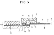
- Figure 3 is an illustration of an assembly under display inspection of a liquid crystal display panel using a connector for display inspection of the invention in COG mounting by a vertical cross sectional view.
- Figures 4A to 4E are each an illustration of one of the steps of the process for the preparation of an inventive connector for display inspection by a vertical cross sectional view.
- the connector for display inspection is an integral assembly which comprises, making reference to figures 2A and 2B illustrating the connector by a vertical cross sectional view and a schematic plan view, respectively:
- a circuit board 5 having input electrode terminals 2 and output electrode terminals 3 connected together with a wiring pattern 4 is mounted on and integrally bonded to a bonding base plate 21 having a larger dimension than the circuit board 5, in exact positioning (step (1a)).
- Each of the output electrode terminals 3 is connected to the bonding base plate by wire bonding by means of a connecting lead wire 6 taking an arch-wise bent configuration bridging the circuit board 5 and the bonding base plate 21 (step (1b)).
- the material of the circuit board 5 is not particularly limitative including various kinds of electrically insulating materials such as glass fiber-reinforced resins, e.g., epoxy resins and BT resins, ceramics, multilayered plates and FPC as well as lead frames, of which glass fiber-reinforced epoxy resin plates are preferred as the material of the circuit board 5 due to economical reasons.
- electrically insulating materials such as glass fiber-reinforced resins, e.g., epoxy resins and BT resins, ceramics, multilayered plates and FPC as well as lead frames, of which glass fiber-reinforced epoxy resin plates are preferred as the material of the circuit board 5 due to economical reasons.
- the metallic material of the connecting lead wires 6 is not particularly limitative including fine filaments of gold, gold-based alloys, copper, aluminum, aluminum-silicon alloys, beryllium copper, brass, nickel. molybdenum, tungsten and stainless steels, if desired,plated with gold or a gold-based alloy, of which gold filaments are preferred,
- the diameter of the connecting lead wires 6 is selected in consideration of the arrangement pitch of the electrode terminals on the liquid crystal display panels under inspection and other factors but is usually in the range from 18 to 50 ⁇ m or, preferably, from 20 to 30 ⁇ m.
- a rigid covering body 7 having an injection port 23 penetrating the upper wall thereof and a cavity or groove 22 on the lower end surface of the downwardly extending side portion thereof is mounted on and fixed to the circuit board 5 in such a fashion of bridging the circuit board 5 and the bonding base plate 21 (step (2a)).
- the connecting lead wires 6 are as a whole covered by and enveloped in the space below the covering body 7.
- the above mentioned void space below the covering body 7 is completely filled with a curable insulating liquid elastomer resin 8 injected thereinto through the injection port 23 in the upper wall of the covering body 7 so that the connecting lead wires 6 are completely embedded in the liquid curable resin 8, which is then subjected to curing, if necessary, by heating to encapsulate the connecting lead wires 6 as a whole (step (2b)).
- the material of the covering body 7 can be selected from various kinds of rigid materials including plastic resins, ceramic materials and metallic materials, of which metallic materials are preferred due to their high dimensional accuracy and mechanical strengths.
- curable liquid elastomer compositions can be used to fill the space below the covering body 7 including silicone rubbers, polybutadiene rubbers, natural rubber, polyisoprene rubbers, urethane rubbers, chloroprene rubbers and styrene-butadiene copolymeric rubbers as well as foamed porous bodies of these rubber materials.
- the rubber material is admixed with an internal priming agent with an object to improve the adhesive bonding between the cured rubbery body 8 and the connecting lead wires 6 embedded therein. It is important to select a rubbery material having adequate elasticity and hardness to facilitate conforming deformation with bending of the connecting lead wires 6 so that a good contacting condition can always be ensured between contact points.
- the above mentioned liquid elastomer resin injected into the space below the covering body 7 has a viscosity in the range from 5 to 1000 poise or, preferably, from 10 to 500 poise.
- a trouble would be caused due to undesired deformation or displacement of the connecting lead wires 6 each forming an arch, if not to mention the difficulty in completely filling the space below the covering body 7, while, when the viscosity of the liquid resin is too low, a trouble would eventually be caused due to leakage of the liquid resin out of the space below the covering body 7.
- the bonding base plate 21 is removed from the circuit board 5 by a suitable means depending on the material thereof such as chemical etching using an etching solution so as to expose the end portion of each of the connecting lead wires 6, which has been bonded in the preceding steps to the bonding base plate 21, out of the cured elastomer body 8 (step (3)).
- each of the connecting lead wires 6 is provided with a plating layer 9 of a metal with an object to improve the corrosion resistance of the end points of the connecting lead wires 6 and to ensure good contacting condition thereof with the electrode terminals of the liquid crystal display panels under inspection.
- the metallic material 9 for this plating is not particularly limitative provided that the above mentioned object can be accomplished including gold, silver, nickel, palladium, rhodium, tin and solder alloys as well as combinations thereof, of which gold is preferred in respect of the low contacting resistance and high corrosion resistance.
- the plating layer of the metal mentioned above has a thickness usually in the range from 1 to 100 ⁇ m or, preferably, from 10 to 50 ⁇ m. When the thickness of the plating layer is too small, desired good contacting condition with the electrode terminals on the display panel cannot be ensured while, when the thickness is too large, the plating layer would be subject to eventual falling or exfoliation.
- an insulating elastomer sheet 10 having a thickness of 0.1 to 2.0 mm or, preferably, 0.5 to 1.0 mm as a cushioning spacer is put into and adhesively bonded onto the bottom surface of the cavity or groove 22, which has a flat bottom surface in parallel to the circuit board 5, of the covering body 7, and a driver IC chip 12 having electrode terminals 11 is adhesively bonded to the cushioning spacer 10.
- the depth of the cavity or groove 22 is selected such that, after fixing the driver IC chip 12 to the cavity or groove 22, the electrode terminals 11 on the driver IC chip 12 and the plated end portions 9 of the connecting lead wires 6 are coplanar or, namely, on one and the same plane in order to ensure a good contacting condition between these contacting points and the electrode terminals on the liquid crystal display panel under inspection.
- FIG 3 is an illustration of a testing assembly in the COG mounting using the above described connector 1 for display inspection by a vertical cross sectional view.
- the connector 1 for display inspection is mounted on a liquid crystal display panel 15 in such a position that the electrode terminals 11 of the driver IC chip 12 are brought into a press-contacting condition with the display output signal delivery electrodes 17 on the glass substrate 16 of the display panel 15 while the end contacting points 9 of the connecting lead wires 6 are brought into a press-contacting condition with the display input signal delivery electrodes 18 on the glass substrate 16.
- display inspection of the liquid crystal display panel 15 can be easily and rapidly conducted by supplying testing signals to the input electrode terminals 2 of the circuit board 5.
- a connector 1 for display inspection of a liquid crystal display panel was prepared in the following manner.
- a circuit board 5 having input electrode terminals 2 and output electrode terminals 3 was mounted in an exactly specified position on a thin bonding base plate 21 of copper and the bonding areas of the bonding base plate 21 was plated with gold. As is illustrated in Figure 4A, the bonding area was selected on the flat bottom surface of a groove of small depth formed on the upper surface of the bonding base plate 21. The recessed bonding area was advantageous because the end portions of the connecting lead wires 6 could be at a level lower than the lower surface of the circuit board 5 to ensure a good contacting condition between contact points.
- a plurality of connecting lead wires 6 were each bonded, at one end, to one of the output electrode terminals 3 and, at the other end, to the gold-plated bonding area on the bonding base plate 21 by using a general-purpose wire bonding machine.
- each of the connecting lead wires 6 was bent in an arched configuration to bridge the output electrode terminal 3 on the circuit board 5 and the bonding area on the bonding base plate 21 as is shown in Figure 4A.
- a rigid covering body 7 of a metal was mounted on and fixed to the circuit board 5 and the bonding base plate 21 in such a fashion as to bridge the circuit board 5 and the bonding base plate 21 and to envelop the arch-wise bent connecting lead wires 6 within the space formed below the covering body 7.
- the covering body 7 was provided in the upper wall with an injection port 23 for injection of a curable liquid resin and an air escape.
- a cavity 22 having a flat bottom surface was formed in the lower end surface of the downwardly extended side portion of the covering body 7. The cavity 22 had plan dimensions just to fit the driver IC chip to be subsequently inserted thereinto.
- a curable liquid resin 8 was poured into the space below the covering body 7 through the injection port 23 in the covering body 7 so that the space was completely filled with the liquid resin.
- the arch-wise bent connecting lead wires 6 were completely embedded as a whole in the liquid resin.
- the curable liquid resin was subsequently cured by heating.
- the bonding base plate 21 was dissolved away by dipping the assembly in an aqueous etching solution containing iron(III) chloride so as to expose the lower surface of the circuit board 5 and the end portions 9 of the connecting lead wires 6 out of the cured elastomer body 8.
- an insulating elastomer sheet 10 coated on both surfaces with an adhesive was put on the bottom surface of the cavity 22 in the covering body 7 and further a driver IC chip 12 having bump-formed electrode terminals 11 was inserted with exact positioning into the cavity 22 so as to be adhesively bonded to the covering body 7 with the insulating elastomer sheet 10 as a cushioning spacer intervening therebetween to complete the connector for display inspection.
Landscapes
- Engineering & Computer Science (AREA)
- Computer Hardware Design (AREA)
- General Physics & Mathematics (AREA)
- Theoretical Computer Science (AREA)
- Physics & Mathematics (AREA)
- Liquid Crystal (AREA)
- Measuring Leads Or Probes (AREA)
- Coupling Device And Connection With Printed Circuit (AREA)
- Devices For Indicating Variable Information By Combining Individual Elements (AREA)
- Multi-Conductor Connections (AREA)
- Manufacturing Of Electrical Connectors (AREA)
- Testing Of Short-Circuits, Discontinuities, Leakage, Or Incorrect Line Connections (AREA)
- Testing Of Individual Semiconductor Devices (AREA)
Applications Claiming Priority (3)
| Application Number | Priority Date | Filing Date | Title |
|---|---|---|---|
| JP33996296 | 1996-12-19 | ||
| JP8339962A JPH10186393A (ja) | 1996-12-19 | 1996-12-19 | 液晶表示パネルの表示検査用コネクタ及びその製造方法 |
| JP339962/96 | 1996-12-19 |
Publications (3)
| Publication Number | Publication Date |
|---|---|
| EP0849603A2 true EP0849603A2 (de) | 1998-06-24 |
| EP0849603A3 EP0849603A3 (de) | 1999-07-21 |
| EP0849603B1 EP0849603B1 (de) | 2004-05-06 |
Family
ID=18332421
Family Applications (1)
| Application Number | Title | Priority Date | Filing Date |
|---|---|---|---|
| EP97121810A Expired - Lifetime EP0849603B1 (de) | 1996-12-19 | 1997-12-11 | Verbinder zur Prüfung von Flüssigkristallanzeigen und Verfahren zu seiner Herstellung |
Country Status (6)
| Country | Link |
|---|---|
| US (1) | US6091475A (de) |
| EP (1) | EP0849603B1 (de) |
| JP (1) | JPH10186393A (de) |
| CN (1) | CN1101065C (de) |
| DE (1) | DE69728956T2 (de) |
| TW (1) | TW353240B (de) |
Families Citing this family (44)
| Publication number | Priority date | Publication date | Assignee | Title |
|---|---|---|---|---|
| US6429120B1 (en) | 2000-01-18 | 2002-08-06 | Micron Technology, Inc. | Methods and apparatus for making integrated-circuit wiring from copper, silver, gold, and other metals |
| US6266119B1 (en) * | 1998-01-13 | 2001-07-24 | Canon Kabushiki Kaisha | Liquid crystal apparatus and production process thereof |
| US6509590B1 (en) * | 1998-07-20 | 2003-01-21 | Micron Technology, Inc. | Aluminum-beryllium alloys for air bridges |
| US6556268B1 (en) * | 1999-03-31 | 2003-04-29 | Industrial Technology Research Institute | Method for forming compact LCD packages and devices formed in which first bonding PCB to LCD panel and second bonding driver chip to PCB |
| US6420262B1 (en) | 2000-01-18 | 2002-07-16 | Micron Technology, Inc. | Structures and methods to enhance copper metallization |
| US7262130B1 (en) | 2000-01-18 | 2007-08-28 | Micron Technology, Inc. | Methods for making integrated-circuit wiring from copper, silver, gold, and other metals |
| US7211512B1 (en) | 2000-01-18 | 2007-05-01 | Micron Technology, Inc. | Selective electroless-plated copper metallization |
| US6423629B1 (en) | 2000-05-31 | 2002-07-23 | Kie Y. Ahn | Multilevel copper interconnects with low-k dielectrics and air gaps |
| US6674167B1 (en) | 2000-05-31 | 2004-01-06 | Micron Technology, Inc. | Multilevel copper interconnect with double passivation |
| JP4649706B2 (ja) * | 2000-06-08 | 2011-03-16 | ソニー株式会社 | 表示装置およびこれを用いた携帯端末 |
| JP2002196298A (ja) * | 2000-12-22 | 2002-07-12 | Fujitsu Ltd | 液晶表示ユニットとその製造方法 |
| US6944032B1 (en) | 2001-04-12 | 2005-09-13 | Rockwell Collins | Interconnect for flat panel displays |
| KR100805127B1 (ko) * | 2001-05-17 | 2008-02-21 | 삼성전자주식회사 | 램프 와이어 고정홈을 갖는 액정표시장치 |
| US7446261B2 (en) | 2001-09-06 | 2008-11-04 | Finisar Corporation | Flexible circuit boards with tooling cutouts for optoelectronic modules |
| US7439449B1 (en) | 2002-02-14 | 2008-10-21 | Finisar Corporation | Flexible circuit for establishing electrical connectivity with optical subassembly |
| US6685487B2 (en) * | 2002-06-12 | 2004-02-03 | Siemens Information & Communication Mobile Llc | Elastomeric connector assembly |
| US7526207B2 (en) * | 2002-10-18 | 2009-04-28 | Finisar Corporation | Flexible circuit design for improved laser bias connections to optical subassemblies |
| CN1316293C (zh) * | 2002-12-10 | 2007-05-16 | 统宝光电股份有限公司 | 平面显示器组装结构 |
| KR20040075377A (ko) * | 2003-02-20 | 2004-08-30 | 삼성전자주식회사 | 구동 아이씨 및 이를 갖는 디스플레이 장치 |
| US7378596B2 (en) * | 2003-04-18 | 2008-05-27 | Ibiden Co., Ltd. | Rigid-flex wiring board |
| US7311240B2 (en) | 2004-04-30 | 2007-12-25 | Finisar Corporation | Electrical circuits with button plated contacts and assembly methods |
| US7306377B2 (en) * | 2004-04-30 | 2007-12-11 | Finisar Corporation | Integrated optical sub-assembly having epoxy chip package |
| US7275937B2 (en) * | 2004-04-30 | 2007-10-02 | Finisar Corporation | Optoelectronic module with components mounted on a flexible circuit |
| US7425135B2 (en) * | 2004-04-30 | 2008-09-16 | Finisar Corporation | Flex circuit assembly |
| JP4536430B2 (ja) * | 2004-06-10 | 2010-09-01 | イビデン株式会社 | フレックスリジッド配線板 |
| US7629537B2 (en) * | 2004-07-09 | 2009-12-08 | Finisar Corporation | Single layer flex circuit |
| TWI288267B (en) * | 2004-09-03 | 2007-10-11 | Innolux Display Corp | Liquid crystal display panel and method of fabricating the circuit substrate of the liquid crystal display panel |
| JP4178417B2 (ja) * | 2005-07-25 | 2008-11-12 | セイコーエプソン株式会社 | 半導体装置の製造方法 |
| TW200719002A (en) * | 2005-11-07 | 2007-05-16 | Au Optronics Corp | Liquid crystal display panel module and flexible printed circuit board thereof |
| JP2007139912A (ja) * | 2005-11-15 | 2007-06-07 | Sharp Corp | 駆動素子実装表示装置 |
| JP4945140B2 (ja) * | 2006-02-01 | 2012-06-06 | テクダイヤ株式会社 | 波長可変光フィルター及びこれを用いた外部共振器型半導体レーザ装置 |
| TWI301201B (en) * | 2006-03-15 | 2008-09-21 | Au Optronics Corp | Display circuits |
| JP4884288B2 (ja) * | 2007-04-27 | 2012-02-29 | 三洋電機株式会社 | コネクタ装置およびその製造方法並びにそれを用いた電池パック |
| CN100451741C (zh) * | 2007-10-16 | 2009-01-14 | 华映视讯(吴江)有限公司 | Ic芯片安装方法、ic芯片安装架构以及液晶显示器 |
| JP2011059149A (ja) * | 2009-09-07 | 2011-03-24 | Hitachi Displays Ltd | 電子機器 |
| KR100991367B1 (ko) * | 2010-03-15 | 2010-11-02 | (주)아테코 | 표시장치용 검사 모듈 |
| CN101908520A (zh) * | 2010-08-03 | 2010-12-08 | 福建合顺微电子有限公司 | 一种引线框架塑胶复合体联接结构 |
| CN104576411A (zh) * | 2013-10-25 | 2015-04-29 | 飞思卡尔半导体公司 | 双角部顶部闸道模制 |
| JP6348759B2 (ja) * | 2014-04-16 | 2018-06-27 | オリンパス株式会社 | 半導体モジュール、接合用治具、および半導体モジュールの製造方法 |
| US20180188290A1 (en) * | 2015-07-03 | 2018-07-05 | Okins Electronics Co.,Ltd | Test socket, test socket manufacturing method, and jig assembly for test socket |
| JP6844455B2 (ja) * | 2017-07-04 | 2021-03-17 | 株式会社オートネットワーク技術研究所 | 回路装置 |
| CN107819447A (zh) * | 2017-09-11 | 2018-03-20 | 上海亚明照明有限公司 | 集线式滤波器 |
| WO2019123647A1 (ja) * | 2017-12-22 | 2019-06-27 | 堺ディスプレイプロダクト株式会社 | 表示装置および表示装置の製造方法 |
| WO2024262025A1 (ja) * | 2023-06-23 | 2024-12-26 | シャープディスプレイテクノロジー株式会社 | 表示装置及びその製造方法、並びにチップ保護体 |
Family Cites Families (17)
| Publication number | Priority date | Publication date | Assignee | Title |
|---|---|---|---|---|
| JPS5237744A (en) * | 1975-09-19 | 1977-03-23 | Seiko Epson Corp | Electronic desk computer with liquid crystal display |
| JPS60130721A (ja) * | 1983-12-19 | 1985-07-12 | Citizen Watch Co Ltd | 液晶表示装置 |
| JPS60238817A (ja) * | 1984-05-12 | 1985-11-27 | Citizen Watch Co Ltd | 液晶表示装置 |
| JPH0682765B2 (ja) * | 1985-12-25 | 1994-10-19 | 株式会社日立製作所 | 液晶表示素子 |
| KR940006185Y1 (ko) * | 1990-06-07 | 1994-09-10 | 가시오 게이상기 가부시끼가이샤 | Ic 모듈 |
| JP2801487B2 (ja) * | 1992-04-30 | 1998-09-21 | シャープ株式会社 | パネルの実装構造および実装方法並びに樹脂供給硬化方法 |
| US5429510A (en) * | 1993-12-01 | 1995-07-04 | Aehr Test Systems, Inc. | High-density interconnect technique |
| US5729316A (en) * | 1994-07-07 | 1998-03-17 | Samsung Electronics Co., Ltd. | Liquid crystal display module |
| US5822030A (en) * | 1994-09-16 | 1998-10-13 | Seiko Epson Corporation | Liquid crystal display device, its mounting structure and electronic device |
| TW378276B (en) * | 1995-01-13 | 2000-01-01 | Seiko Epson Corp | Liquid crystal display device and its fabrication method |
| WO1997001791A1 (en) * | 1995-06-29 | 1997-01-16 | Philips Electronics N.V. | Display device |
| JP2730536B2 (ja) * | 1995-12-27 | 1998-03-25 | 日本電気株式会社 | 液晶表示装置 |
| JPH09297318A (ja) * | 1996-03-06 | 1997-11-18 | Seiko Epson Corp | 液晶装置、液晶装置の製造方法および電子機器 |
| JP3423855B2 (ja) * | 1996-04-26 | 2003-07-07 | 株式会社デンソー | 電子部品搭載用構造体および電子部品の実装方法 |
| US5738530A (en) * | 1996-05-28 | 1998-04-14 | Packard Hughes Interconnect Company | Contact pad having metallically anchored elastomeric electrical contacts |
| US5860815A (en) * | 1997-02-21 | 1999-01-19 | Minnesota Mining And Manufacturing Company | Edge mount connector having location recesses for solder tail registration |
| US5777705A (en) * | 1997-05-30 | 1998-07-07 | International Business Machines Corporation | Wire bond attachment of a liquid crystal display tile to a tile carrier |
-
1996
- 1996-12-19 JP JP8339962A patent/JPH10186393A/ja active Pending
-
1997
- 1997-12-09 US US08/987,359 patent/US6091475A/en not_active Expired - Lifetime
- 1997-12-10 TW TW086118572A patent/TW353240B/zh not_active IP Right Cessation
- 1997-12-11 DE DE69728956T patent/DE69728956T2/de not_active Expired - Lifetime
- 1997-12-11 EP EP97121810A patent/EP0849603B1/de not_active Expired - Lifetime
- 1997-12-19 CN CN97129778A patent/CN1101065C/zh not_active Expired - Fee Related
Also Published As
| Publication number | Publication date |
|---|---|
| TW353240B (en) | 1999-02-21 |
| DE69728956T2 (de) | 2005-10-06 |
| JPH10186393A (ja) | 1998-07-14 |
| EP0849603A3 (de) | 1999-07-21 |
| EP0849603B1 (de) | 2004-05-06 |
| CN1101065C (zh) | 2003-02-05 |
| US6091475A (en) | 2000-07-18 |
| CN1193827A (zh) | 1998-09-23 |
| DE69728956D1 (de) | 2004-06-09 |
Similar Documents
| Publication | Publication Date | Title |
|---|---|---|
| EP0849603B1 (de) | Verbinder zur Prüfung von Flüssigkristallanzeigen und Verfahren zu seiner Herstellung | |
| US7501584B2 (en) | Circuit board device and method for board-to-board connection | |
| US5933018A (en) | Liquid crystal display panel inspection device and method for manufacturing same | |
| JPH0935789A (ja) | 異方導電性シートおよびその製造方法 | |
| EP0921401B1 (de) | Sonde und Verfahren zur Prüfung einer elektrischen Leiterplatte | |
| CN1175271C (zh) | 液晶显示屏的检验装置和检验方法及其制造方法 | |
| US4970780A (en) | Method for the assemblage of a semiconductor device | |
| JPH09274054A (ja) | プローバー | |
| KR20030037279A (ko) | 엘시디 검사용 프로브 카드 | |
| JPH031560A (ja) | 樹脂封止用回路基板 | |
| US11933837B2 (en) | Inspection jig, and inspection device | |
| JP2004212148A (ja) | プローブカード及びコンタクトプローブの接合固定方法 | |
| JP3163626B2 (ja) | 回路基板検査用アダプター装置の製造方法および回路基板検査用アダプター装置 | |
| JP2002350480A (ja) | 電気検査治具。 | |
| KR20050042563A (ko) | 프로브 카드의 프로브 핀 블록 | |
| CN223624751U (zh) | 一种垂直导电胶 | |
| KR200262944Y1 (ko) | 엘시디 검사용 프로브 카드 | |
| JP3039278U (ja) | 検査用プローブおよび検査用プローブユニット | |
| JPH02273725A (ja) | 液晶表示素子の接続構造体 | |
| JPH10229270A (ja) | 複合基板 | |
| JPS5826529Y2 (ja) | 固定プロ−ブボ−ド | |
| JP3822683B2 (ja) | コンタクトプローブおよびこれを用いたプローブ装置 | |
| JP3015654U (ja) | Qfp検査装置 | |
| JPH10301128A (ja) | 複数電極を有する表示素子及びその外部端子接続装置 | |
| JPH0662370U (ja) | 絶縁板貫通型狭間隔プローバー |
Legal Events
| Date | Code | Title | Description |
|---|---|---|---|
| PUAI | Public reference made under article 153(3) epc to a published international application that has entered the european phase |
Free format text: ORIGINAL CODE: 0009012 |
|
| AK | Designated contracting states |
Kind code of ref document: A2 Designated state(s): DE FR GB NL |
|
| AX | Request for extension of the european patent |
Free format text: AL;LT;LV;MK;RO;SI |
|
| PUAL | Search report despatched |
Free format text: ORIGINAL CODE: 0009013 |
|
| AK | Designated contracting states |
Kind code of ref document: A3 Designated state(s): AT BE CH DE DK ES FI FR GB GR IE IT LI LU MC NL PT SE |
|
| AX | Request for extension of the european patent |
Free format text: AL;LT;LV;MK;RO;SI |
|
| 17P | Request for examination filed |
Effective date: 19990909 |
|
| AKX | Designation fees paid |
Free format text: DE FR GB NL |
|
| GRAH | Despatch of communication of intention to grant a patent |
Free format text: ORIGINAL CODE: EPIDOS IGRA |
|
| GRAS | Grant fee paid |
Free format text: ORIGINAL CODE: EPIDOSNIGR3 |
|
| GRAA | (expected) grant |
Free format text: ORIGINAL CODE: 0009210 |
|
| AK | Designated contracting states |
Kind code of ref document: B1 Designated state(s): DE FR GB NL |
|
| REG | Reference to a national code |
Ref country code: GB Ref legal event code: FG4D |
|
| REF | Corresponds to: |
Ref document number: 69728956 Country of ref document: DE Date of ref document: 20040609 Kind code of ref document: P |
|
| ET | Fr: translation filed | ||
| PLBE | No opposition filed within time limit |
Free format text: ORIGINAL CODE: 0009261 |
|
| STAA | Information on the status of an ep patent application or granted ep patent |
Free format text: STATUS: NO OPPOSITION FILED WITHIN TIME LIMIT |
|
| 26N | No opposition filed |
Effective date: 20050208 |
|
| PGFP | Annual fee paid to national office [announced via postgrant information from national office to epo] |
Ref country code: NL Payment date: 20091216 Year of fee payment: 13 |
|
| PGFP | Annual fee paid to national office [announced via postgrant information from national office to epo] |
Ref country code: GB Payment date: 20091209 Year of fee payment: 13 Ref country code: FR Payment date: 20091221 Year of fee payment: 13 |
|
| PGFP | Annual fee paid to national office [announced via postgrant information from national office to epo] |
Ref country code: DE Payment date: 20091203 Year of fee payment: 13 |
|
| REG | Reference to a national code |
Ref country code: NL Ref legal event code: V1 Effective date: 20110701 |
|
| GBPC | Gb: european patent ceased through non-payment of renewal fee |
Effective date: 20101211 |
|
| REG | Reference to a national code |
Ref country code: FR Ref legal event code: ST Effective date: 20110831 |
|
| PG25 | Lapsed in a contracting state [announced via postgrant information from national office to epo] |
Ref country code: FR Free format text: LAPSE BECAUSE OF NON-PAYMENT OF DUE FEES Effective date: 20110103 |
|
| REG | Reference to a national code |
Ref country code: DE Ref legal event code: R119 Ref document number: 69728956 Country of ref document: DE Effective date: 20110701 |
|
| PG25 | Lapsed in a contracting state [announced via postgrant information from national office to epo] |
Ref country code: DE Free format text: LAPSE BECAUSE OF NON-PAYMENT OF DUE FEES Effective date: 20110701 Ref country code: GB Free format text: LAPSE BECAUSE OF NON-PAYMENT OF DUE FEES Effective date: 20101211 |
|
| PG25 | Lapsed in a contracting state [announced via postgrant information from national office to epo] |
Ref country code: NL Free format text: LAPSE BECAUSE OF NON-PAYMENT OF DUE FEES Effective date: 20110701 |