EP0814395A2 - Überstrommessungsvorrichtung für Leistungs-MOS-Feldeffekttransistor - Google Patents
Überstrommessungsvorrichtung für Leistungs-MOS-Feldeffekttransistor Download PDFInfo
- Publication number
- EP0814395A2 EP0814395A2 EP97109957A EP97109957A EP0814395A2 EP 0814395 A2 EP0814395 A2 EP 0814395A2 EP 97109957 A EP97109957 A EP 97109957A EP 97109957 A EP97109957 A EP 97109957A EP 0814395 A2 EP0814395 A2 EP 0814395A2
- Authority
- EP
- European Patent Office
- Prior art keywords
- mos transistor
- sensing
- overcurrent
- voltage
- source
- Prior art date
- Legal status (The legal status is an assumption and is not a legal conclusion. Google has not performed a legal analysis and makes no representation as to the accuracy of the status listed.)
- Withdrawn
Links
Images


Classifications
-
- G—PHYSICS
- G01—MEASURING; TESTING
- G01R—MEASURING ELECTRIC VARIABLES; MEASURING MAGNETIC VARIABLES
- G01R31/00—Arrangements for testing electric properties; Arrangements for locating electric faults; Arrangements for electrical testing characterised by what is being tested not provided for elsewhere
- G01R31/26—Testing of individual semiconductor devices
- G01R31/2607—Circuits therefor
- G01R31/2621—Circuits therefor for testing field effect transistors, i.e. FET's
-
- G—PHYSICS
- G01—MEASURING; TESTING
- G01R—MEASURING ELECTRIC VARIABLES; MEASURING MAGNETIC VARIABLES
- G01R19/00—Arrangements for measuring currents or voltages or for indicating presence or sign thereof
- G01R19/0092—Arrangements for measuring currents or voltages or for indicating presence or sign thereof measuring current only
-
- G—PHYSICS
- G01—MEASURING; TESTING
- G01R—MEASURING ELECTRIC VARIABLES; MEASURING MAGNETIC VARIABLES
- G01R31/00—Arrangements for testing electric properties; Arrangements for locating electric faults; Arrangements for electrical testing characterised by what is being tested not provided for elsewhere
- G01R31/26—Testing of individual semiconductor devices
- G01R31/2644—Adaptations of individual semiconductor devices to facilitate the testing thereof
-
- H—ELECTRICITY
- H03—ELECTRONIC CIRCUITRY
- H03K—PULSE TECHNIQUE
- H03K17/00—Electronic switching or gating, i.e. not by contact-making and –breaking
- H03K17/08—Modifications for protecting switching circuit against overcurrent or overvoltage
- H03K17/082—Modifications for protecting switching circuit against overcurrent or overvoltage by feedback from the output to the control circuit
- H03K17/0822—Modifications for protecting switching circuit against overcurrent or overvoltage by feedback from the output to the control circuit in field-effect transistor switches
-
- H—ELECTRICITY
- H02—GENERATION; CONVERSION OR DISTRIBUTION OF ELECTRIC POWER
- H02M—APPARATUS FOR CONVERSION BETWEEN AC AND AC, BETWEEN AC AND DC, OR BETWEEN DC AND DC, AND FOR USE WITH MAINS OR SIMILAR POWER SUPPLY SYSTEMS; CONVERSION OF DC OR AC INPUT POWER INTO SURGE OUTPUT POWER; CONTROL OR REGULATION THEREOF
- H02M1/00—Details of apparatus for conversion
- H02M1/0003—Details of control, feedback or regulation circuits
- H02M1/0009—Devices or circuits for detecting current in a converter
-
- H—ELECTRICITY
- H03—ELECTRONIC CIRCUITRY
- H03K—PULSE TECHNIQUE
- H03K2217/00—Indexing scheme related to electronic switching or gating, i.e. not by contact-making or -breaking covered by H03K17/00
- H03K2217/0027—Measuring means of, e.g. currents through or voltages across the switch
Definitions
- the present invention relates to a semiconductor device, and particularly to an overcurrent sensing circuit that senses an overcurrent flowing in a power MOS field effect transistor.
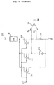
- Fig. 1 shows one example of such a circuit disclosed in US Patent No. 4, 553, 084.
- Power MOS transistor 30 is a transistor comprising 3,000 or more cell transistors, the gates, drains, and sources of each being connected in parallel, and has its source connected to ground 25 and its drain connected to power supply 29 by way of load 31.
- MOS transistors 24 and 27 are both of a single-cell structure and, similarly to the drain of MOS transistor 30, both have their drains connected to load 31. MOS transistors 24 and 27 also have their sources connected to ground 25, MOS transistor 24 by way of constant-current source 26 and MOS transistor 27 by way of sensing resistor 28.
- Comparator 33 has its first input terminal 34 connected to the source of MOS transistor 24 and its second input terminal 35 connected to the source of MOS transistor 27, and the output of comparator 33 is connected to output terminal 36.
- a gate drive (not shown) controls the gates of these MOS transistors 30, 24, and 27 in common by way of gate terminal 37.
- the current flowing through MOS transistor 27 is approximately 3 milliamperes, and accordingly, the voltage drop of sensing resistor 28 of approximately 100 millivolts is supplied to terminal 35 of comparator 33. Consequently, the current flowing in sensing resistor 28 is insignificant and its voltage drop is also small and has almost no effect on the load current. Moreover, the voltage drop of this sensing resistor 28 is proportional to the value of the current flowing, and this current value is proportional to the load current value flowing through power MOS transistor 30. Accordingly, the current flowing through sensing resistor 28 can be used for sensing the overcurrent of the load current flowing through power MOS transistor 30.
- Comparator 33 is used to detect whether or not the current is equal to the current flowing through constant-current source 26. When the current is equal to or below this value, the output of comparator 33 is 0. If the current of sensing resistor 28 exceeds the current of constant-current source 26, comparator 33 outputs a high-level signal warning of an overcurrent.
- the current of constant-current source 26 that serves as the alert standard can be set arbitrarily.
- Fig. 2 shows an equivalent circuit diagram of the principal components of a semiconductor device disclosed in Japanese Utility Model No. 32543/92.
- Power MOSFET 41 of this example of the prior art is composed of a large number of MOSFET elements arranged in parallel similar to power MOS transistor 30 of the first example of the prior art described hereinabove, and each of the sources, gates, and drains of the unit elements are coupled in parallel to form a source, gate, and drain as for a single element.
- This example is characterized by forming, within the same element as output power MOSFET 41, an overcurrent sensing circuit section that senses an overcurrent flowing through output power MOSFET 41 and load 47 by sensing the voltage drop across both ends of source wiring resistor 42 of this power MOSFET 41.
- the object of the present invention is to provide an overcurrent sensing circuit that enables free setting of the overcurrent sensing value, and moreover, allows a reduction of the influence of variations in characteristic that occur in manufacture.
- the overcurrent sensing circuit of the present invention senses overcurrent conditions of a power MOS transistor that has its drain connected to a power supply and that supplies electrical power to a load from its source.
- An MOS transistor for sensing overcurrent flowing through the power MOS transistor has its drain and gate connected to the drain and gate, respectively, of the power MOS transistor.
- a sensing resistor is connected between the source of the sensing MOS transistor and the source of the power MOS transistor and has a resistance value sufficiently greater than the ON resistance value of the sensing MOS transistor.
- a comparator having an offset voltage has its two input terminals connected to the two terminals of the sensing resistor, inputs from these input terminals a voltage drop value due to the sense current flowing through the sensing resistor, and outputs an overcurrent sensing signal when this voltage drop value exceeds an input offset voltage value that is set internally.
- a power MOS transistor is formed as a single MOS transistor in which the drains, sources, and gates of a large plurality of cell-unit transistors are connected in parallel; and the sensing MOS transistor is formed from a cell-unit transistor of the same cell-unit.
- a sufficiently great resistance value of the sensing resistor is a value such that a voltage drop can be obtained that is equal to the voltage across the drain and source of the power MOS transistor.
- the comparator having an offset voltage includes at least a differential input stage that takes as input the voltage drop of the sensing resistor, an output stage, and a bias circuit; and allows intentional setting of the input offset voltage by disrupting the balance in the size of paired transistors that make up the differential input stage.
- the sensing resistor has a resistance value that is sufficiently greater than the ON resistance of the sensing MOS transistor, and therefore, a voltage drop can be obtained that it is equal to the voltage across the drain and source of the power MOS transistor, which is the object of overcurrent sensing.
- the range of variation in the threshold voltage Vt of the power MOS transistor at manufacture is on the order of ⁇ 0.3 V, and by sufficiently impressing a voltage between the gate and source, variation in the ON resistance caused by variation in the threshold voltage can be ignored.
- Variation in the resistivity of the semiconductor substrate on which the power MOS transistor is formed is kept within the range of ⁇ 10%, and as a result, variation in the ON resistance is also on the order of ⁇ 10%, a value that is considerably lower than a diffused resistors, which has variation on the order of ⁇ 30%.
- variation in overcurrent sensing values between differing elements may be considered to be influenced only by variation in the resistance value that sets the value of the input offset voltage of the comparator, i.e., the constant current flowing through the bias circuit within the comparator.
- the input offset voltage of the comparator is proportional to the square root of the constant current value of the bias circuit, and as a result, this voltage is proportional to the square root of the resistance value of the bias circuit, thereby allowing a reduction in variation in the overcurrent sensing value of the power MOS transistor.
- Fig. 1 is a circuit diagram showing one example of an overcurrent sensing circuit of the prior art.
- Fig. 2 is a circuit diagram showing another example of an overcurrent sensing circuit of the prior art.
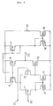
- Fig. 3 is a circuit diagram showing an embodiment of the overcurrent sensing circuit of the present invention.
- Fig. 4 is a equivalent circuit diagram showing an ordinary comparator.
- power MOS transistor 2 which is the object of overcurrent sensing, is constructed from a large number of cell-unit transistors having gates, drains, and sources connected in parallel, the sources are connected to ground 8 by way of load 7, and the drains are connected to power supply 4.
- the overcurrent sensing circuit is composed of sensing MOS transistor 3, sensing resistor 5, and offset voltage-added comparator 6; and sensing MOS transistor 3 is composed of one identical cell unit having its drain connected to power supply 4 and its source connected to the source of power MOS transistor 2 by way of sensing resistor 5.
- a gate drive (not shown) controls the gates of power MOS transistor 2 and sensing MOS transistor 3 by way of gate terminal 1.
- Offset voltage-added comparator 6 has its positive input terminal to one end of sensing resistor 5, its negative input terminal connected to the other end of sensing resistor 5, and outputs a sensing signal from output terminal 9.
- Sensing resistor 5 has a resistance value that is sufficiently greater than the ON resistance of sensing MOS transistor 3, a sufficiently greater resistance value being a value such that a voltage drop can be obtained that is equal to the voltage across the drain and source of power MOS transistor 2.
- sensing resistor 5 has a sufficiently large resistance value compared with the ON resistance of sensing MOS transistor 3, this voltage drop is substantially equal to the voltage across the drain and source of power MOS transistor 2. Accordingly, when power MOS transistor 2 enters an overcurrent state, the voltage across its drain and source changes, and when this voltage equals or exceeds the input offset voltage of offset voltage-added comparator 6, the sensing signal reverses.
- Fig. 4 is a circuit diagram showing the structure of an ordinary comparator.
- the comparator is made up of a differential input stage made up of MOS transistors 10, 11, 12, 13, and 14; an output stage made up of MOS transistors 15 and 16; and a bias circuit made up of MOS transistors 17, 18, and 19 and resistor 20.
- these circuits operate as one comparator that compares these voltages and outputs an output signal from output terminal 23.
- the bias circuit is the bias source for the differential input stage and output stage and constitutes a constant-current source.
- the bias current of this circuit determines the current value of MOS transistors 10 and 15. In other words, MOS transistors 10 and 15 are in a uniform operation state.
- an input offset voltage is set within the comparator beforehand instead of setting an offset voltage to the comparator from the outside as described hereinabove, and the level of the output terminal is reversed when the value of voltage inputted between the positive and negative input terminals exceeds this input offset voltage value.
- this method arrives at a setting by selecting input offset voltages by varying ratio A between W 11 /L 11 and W 12 /L 12 which are, the area ratio of paired transistors 11 and 12, respectively.
- the input offset voltage V OS increases in proportion to the square root of bias current I and therefore can increase to a greater degree than shown in Table 1.
- the input offset voltage of the comparator is established by equation (1), and input offset voltage originating in W is influenced by variation in the bias current I.
- Variation in the bias current depends on variation in the resistance of resistor 20 of the bias circuit. If variation is assumed to be 30% of the resistance value, the variation in the intentionally set input offset voltage is seen to be proportional to the square root of bias current I according to equation (1), and since the square root of 1.30 is 1.14, the variation is 14%.
Landscapes
- Physics & Mathematics (AREA)
- General Physics & Mathematics (AREA)
- Engineering & Computer Science (AREA)
- Microelectronics & Electronic Packaging (AREA)
- Measurement Of Current Or Voltage (AREA)
- Emergency Protection Circuit Devices (AREA)
- Electronic Switches (AREA)
- Amplifiers (AREA)
- Testing Of Short-Circuits, Discontinuities, Leakage, Or Incorrect Line Connections (AREA)
- Metal-Oxide And Bipolar Metal-Oxide Semiconductor Integrated Circuits (AREA)
- Protection Of Static Devices (AREA)
- Control Of Voltage And Current In General (AREA)
Applications Claiming Priority (2)
| Application Number | Priority Date | Filing Date | Title |
|---|---|---|---|
| JP161744/96 | 1996-06-21 | ||
| JP8161744A JPH1014099A (ja) | 1996-06-21 | 1996-06-21 | 過電流検出回路 |
Publications (2)
| Publication Number | Publication Date |
|---|---|
| EP0814395A2 true EP0814395A2 (de) | 1997-12-29 |
| EP0814395A3 EP0814395A3 (de) | 1998-10-28 |
Family
ID=15741069
Family Applications (1)
| Application Number | Title | Priority Date | Filing Date |
|---|---|---|---|
| EP97109957A Withdrawn EP0814395A3 (de) | 1996-06-21 | 1997-06-18 | Überstrommessungsvorrichtung für Leistungs-MOS-Feldeffekttransistor |
Country Status (3)
| Country | Link |
|---|---|
| US (1) | US5903422A (de) |
| EP (1) | EP0814395A3 (de) |
| JP (1) | JPH1014099A (de) |
Cited By (9)
| Publication number | Priority date | Publication date | Assignee | Title |
|---|---|---|---|---|
| EP0881769A2 (de) * | 1997-05-30 | 1998-12-02 | Nec Corporation | Überstromdetektor und damit ausgestattete Lasttreiberschaltung |
| EP1017173A2 (de) * | 1998-12-28 | 2000-07-05 | Yazaki Corporation | Spannungsversorgungs-Steuervorrichtung und entprechendes Steuerverfahren |
| EP1028526A2 (de) * | 1999-02-14 | 2000-08-16 | Yazaki Corporation | Schaltungsanordnung mit Detektion von Leckströmen |
| WO2001089053A1 (de) * | 2000-05-16 | 2001-11-22 | Robert Bosch Gmbh | Halbleiter-bauelement |
| WO2002037671A1 (en) * | 2000-08-23 | 2002-05-10 | Intersil Americas Inc. | Integrated circuit with current sense circuit and associated methods |
| FR2839365A1 (fr) * | 2002-05-03 | 2003-11-07 | Bosch Gmbh Robert | Dispositif et procede de mesure du courant d'excitation d'un transistor de reference |
| EP3442019A4 (de) * | 2016-04-06 | 2019-12-04 | Shindengen Electric Manufacturing Co., Ltd. | Leistungsmodul |
| CN111370477A (zh) * | 2018-12-25 | 2020-07-03 | 上海新微技术研发中心有限公司 | 具有过流限制功能的绝缘栅双极型晶体管及其构建方法 |
| CN113495184A (zh) * | 2021-07-28 | 2021-10-12 | 苏州贝克微电子有限公司 | 一种电流检测装置 |
Families Citing this family (49)
| Publication number | Priority date | Publication date | Assignee | Title |
|---|---|---|---|---|
| EP0955724B1 (de) * | 1998-05-08 | 2010-10-13 | STMicroelectronics Srl | Kurzschluss-Schutzschaltung, insbesondere für Leistungstransistoren |
| JP3805543B2 (ja) * | 1998-11-19 | 2006-08-02 | 三菱電機株式会社 | 半導体集積回路 |
| JP3631933B2 (ja) * | 1999-02-14 | 2005-03-23 | 矢崎総業株式会社 | スイッチングデバイス |
| DE19945432A1 (de) * | 1999-09-22 | 2001-04-12 | Infineon Technologies Ag | Schaltungsanordnung zum Ansteuern einer Last mit reduzierter Störabstrahlung |
| JP2001228219A (ja) | 2000-02-17 | 2001-08-24 | Mitsubishi Electric Corp | 半導体装置およびその耐圧不良自己検出システム |
| US6570748B2 (en) | 2000-07-13 | 2003-05-27 | Sipex Corporation | Method and apparatus for indicating an over-current condition |
| JP2002043916A (ja) * | 2000-07-28 | 2002-02-08 | Matsushita Electric Ind Co Ltd | 電圧検出回路および半導体装置 |
| US6531898B2 (en) | 2000-11-30 | 2003-03-11 | Agilent Technologies, Inc. | Device using a detection circuit to determine whether an output current thereof is source-induced or load-induced, and method therefor |
| US6614637B1 (en) * | 2001-07-20 | 2003-09-02 | National Semiconductor Corporation | Apparatus and method for a discharge interrupt circuit that can operate at a low supply voltage |
| US20030185269A1 (en) * | 2002-03-26 | 2003-10-02 | Gutin Mikhail A. | Fiber-coupled vertical-cavity surface emitting laser |
| JP3681374B2 (ja) * | 2002-12-19 | 2005-08-10 | 株式会社日立製作所 | 電流検出装置及びそれを用いたpwmインバータ |
| KR100540229B1 (ko) * | 2003-02-25 | 2006-01-10 | 엘지전자 주식회사 | 이동통신 단말기의 송신단 성능 개선 장치 및 그 방법 |
| JP4068022B2 (ja) * | 2003-07-16 | 2008-03-26 | Necエレクトロニクス株式会社 | 過電流検出回路及び負荷駆動回路 |
| JP2005260658A (ja) * | 2004-03-12 | 2005-09-22 | Nec Electronics Corp | 半導体装置 |
| US7142401B2 (en) * | 2004-03-19 | 2006-11-28 | Freescale Semiconductor, Inc. | Detecting overcurrents in a switching regulator using a voltage dependent reference |
| US7019581B1 (en) * | 2004-06-03 | 2006-03-28 | National Semiconductor Corporation | Current sense circuit |
| US7075373B2 (en) * | 2004-11-02 | 2006-07-11 | Micrel, Inc. | Overcurrent protection circuit with fast current limiting control |
| JP4672443B2 (ja) * | 2005-05-31 | 2011-04-20 | ローム株式会社 | 降圧型スイッチングレギュレータ、その制御回路、ならびにそれを用いた電子機器 |
| JP4713963B2 (ja) | 2005-07-07 | 2011-06-29 | 矢崎総業株式会社 | 過電流検出装置 |
| US7336085B2 (en) * | 2006-02-17 | 2008-02-26 | Infineon Technologies Ag | Current sensing circuit |
| JP4845549B2 (ja) * | 2006-03-23 | 2011-12-28 | ローム株式会社 | 電源装置及びこれを備えた電気機器 |
| JP4770577B2 (ja) * | 2006-05-12 | 2011-09-14 | ソニー株式会社 | 固体撮像装置 |
| JP4855886B2 (ja) * | 2006-10-02 | 2012-01-18 | 株式会社東芝 | 電力増幅装置 |
| KR101365752B1 (ko) * | 2007-04-19 | 2014-02-21 | 페어차일드코리아반도체 주식회사 | 스위칭 모드 파워 서플라이 및 이를 위한 스위치 |
| JP5044448B2 (ja) * | 2008-03-03 | 2012-10-10 | ルネサスエレクトロニクス株式会社 | 電源スイッチ回路 |
| DE102008018244B3 (de) * | 2008-04-10 | 2009-11-19 | Continental Automotive Gmbh | Vorrichtung und Verfahren zum Erkennen eines Fehlers in einer Leistungsbrückenschaltung |
| JP2009277930A (ja) * | 2008-05-15 | 2009-11-26 | Nec Electronics Corp | 半導体装置 |
| US7986149B2 (en) * | 2008-08-19 | 2011-07-26 | Infineon Technologies Austria Ag | System and method for adaptive load fault detection |
| JP5266084B2 (ja) * | 2009-02-17 | 2013-08-21 | ルネサスエレクトロニクス株式会社 | 過電流保護回路 |
| JP2010226789A (ja) * | 2009-03-19 | 2010-10-07 | Oki Semiconductor Co Ltd | 過電流検出回路および電源装置 |
| US7852148B2 (en) * | 2009-03-27 | 2010-12-14 | Semiconductor Components Industries, Llc | Method of forming a sensing circuit and structure therefor |
| JP5431994B2 (ja) * | 2010-02-10 | 2014-03-05 | ルネサスエレクトロニクス株式会社 | 電流制限回路 |
| JP5581907B2 (ja) | 2010-09-01 | 2014-09-03 | 株式会社リコー | 半導体集積回路及び半導体集積回路装置 |
| TWI554030B (zh) * | 2010-10-20 | 2016-10-11 | 羅姆股份有限公司 | 高壓側開關電路、界面電路及電子機器 |
| US20140062521A1 (en) * | 2011-04-25 | 2014-03-06 | Sharp Kabushiki Kaisha | Wiring defect inspecting method, wiring defect inspecting apparatus, and method for manufacturing semiconductor substrate |
| CN102768300A (zh) * | 2012-07-31 | 2012-11-07 | 圣邦微电子(北京)股份有限公司 | 电流检测电路 |
| BE1022018B1 (fr) * | 2013-08-14 | 2016-02-04 | Cockerill Maintenance & Ingenierie S.A. | Dispositif de commutation et protection a distance de systemes electriques. |
| US9739811B2 (en) * | 2014-04-29 | 2017-08-22 | Texas Intruments Incorporated | Overcurrent detector |
| TWI537568B (zh) * | 2015-02-02 | 2016-06-11 | 天鈺科技股份有限公司 | 電流偵測電路與電源積體電路 |
| US10498131B2 (en) * | 2016-12-30 | 2019-12-03 | Infineon Technologies Ag | Electronic switch and protection circuit |
| CN107942120B (zh) * | 2017-10-17 | 2023-06-13 | 深圳南云微电子有限公司 | 电流检测电路和电流检测方法 |
| US11150300B2 (en) | 2019-12-16 | 2021-10-19 | Analog Devices International Unlimited Company | Adaptive blanking of over current fault detection circuits in power conversion gate drivers |
| CN111277253A (zh) * | 2019-12-31 | 2020-06-12 | 启攀微电子(上海)有限公司 | 一种具备恒流功能的高压负载开关电路 |
| CN111273073B (zh) * | 2020-03-31 | 2022-05-20 | 吉林华微电子股份有限公司 | Igbt芯片及半导体功率模块 |
| KR20220009620A (ko) * | 2020-07-16 | 2022-01-25 | 삼성전자주식회사 | 회로 결함 검출 방법 및 장치 |
| US11362504B2 (en) * | 2020-07-20 | 2022-06-14 | Analog Devices International Unlimited Company | Over current sensing scheme for switch applications |
| CN112701663B (zh) * | 2020-12-25 | 2023-10-20 | 上海东软载波微电子有限公司 | 用于功率mos管的过流检测和保护电路、以及功率mos管组件 |
| TWI770740B (zh) * | 2020-12-28 | 2022-07-11 | 致茂電子股份有限公司 | 電子負載設備 |
| WO2022181581A1 (ja) * | 2021-02-25 | 2022-09-01 | パナソニックIpマネジメント株式会社 | オン電圧測定回路 |
Citations (4)
| Publication number | Priority date | Publication date | Assignee | Title |
|---|---|---|---|---|
| EP0326968A1 (de) * | 1988-01-31 | 1989-08-09 | Nec Corporation | Steuerschaltung mit elektrischen Kenndaten, veränderbar in Abhängigkeit vom Lastwiderstand |
| EP0499921A2 (de) * | 1991-02-18 | 1992-08-26 | STMicroelectronics S.r.l. | Stromregelungseinrichtung, insbesondere für Leistungsschaltungen in MOS-Technologie |
| US5473276A (en) * | 1992-05-15 | 1995-12-05 | Nissan Motor Co., Ltd. | MOS type power semiconductor switching device capable of protecting load shortcircuit problem under low heat dissipation |
| US5497285A (en) * | 1993-09-14 | 1996-03-05 | International Rectifier Corporation | Power MOSFET with overcurrent and over-temperature protection |
Family Cites Families (14)
| Publication number | Priority date | Publication date | Assignee | Title |
|---|---|---|---|---|
| US4553084A (en) * | 1984-04-02 | 1985-11-12 | Motorola, Inc. | Current sensing circuit |
| US4573099A (en) * | 1984-06-29 | 1986-02-25 | At&T Bell Laboratories | CMOS Circuit overvoltage protection |
| JPS628966A (ja) * | 1985-07-05 | 1987-01-16 | Nitto Electric Ind Co Ltd | ウエハとリングフレ−ムの貼り合せ方法ならびに装置 |
| GB2222497A (en) * | 1988-09-05 | 1990-03-07 | Philips Electronic Associated | Operational amplifier |
| EP0360884A1 (de) * | 1988-09-26 | 1990-04-04 | Siemens Aktiengesellschaft | CMOS-Differentialkomparator mit Offsetspannung |
| US4987327A (en) * | 1989-05-30 | 1991-01-22 | Motorola, Inc. | Apparatus for adjusting DC offset voltage |
| JP3011727B2 (ja) * | 1989-10-26 | 2000-02-21 | 富士電機株式会社 | 過電流検出回路 |
| JP2646434B2 (ja) * | 1990-05-29 | 1997-08-27 | 日鉱亜鉛 株式会社 | 着色亜鉛めっき方法 |
| JPH05315852A (ja) * | 1992-05-12 | 1993-11-26 | Fuji Electric Co Ltd | 電流制限回路および電流制限回路用定電圧源 |
| US5272392A (en) * | 1992-12-04 | 1993-12-21 | North American Philips Corporation | Current limited power semiconductor device |
| JPH06188641A (ja) * | 1992-12-17 | 1994-07-08 | Fuji Electric Co Ltd | 電流検出装置および電流制限装置 |
| US5550702A (en) * | 1994-11-21 | 1996-08-27 | Texas Instruments Incorporated | Adaptive duty-cycle limiting for overload protection of integrated circuits |
| JPH08154022A (ja) * | 1994-11-29 | 1996-06-11 | Nec Corp | 過電流保護回路付き増幅回路 |
| US5789974A (en) * | 1996-07-17 | 1998-08-04 | Analog Devices, Inc. | Calibrating the DC-offset of amplifiers |
-
1996
- 1996-06-21 JP JP8161744A patent/JPH1014099A/ja active Pending
-
1997
- 1997-06-17 US US08/877,647 patent/US5903422A/en not_active Expired - Fee Related
- 1997-06-18 EP EP97109957A patent/EP0814395A3/de not_active Withdrawn
Patent Citations (4)
| Publication number | Priority date | Publication date | Assignee | Title |
|---|---|---|---|---|
| EP0326968A1 (de) * | 1988-01-31 | 1989-08-09 | Nec Corporation | Steuerschaltung mit elektrischen Kenndaten, veränderbar in Abhängigkeit vom Lastwiderstand |
| EP0499921A2 (de) * | 1991-02-18 | 1992-08-26 | STMicroelectronics S.r.l. | Stromregelungseinrichtung, insbesondere für Leistungsschaltungen in MOS-Technologie |
| US5473276A (en) * | 1992-05-15 | 1995-12-05 | Nissan Motor Co., Ltd. | MOS type power semiconductor switching device capable of protecting load shortcircuit problem under low heat dissipation |
| US5497285A (en) * | 1993-09-14 | 1996-03-05 | International Rectifier Corporation | Power MOSFET with overcurrent and over-temperature protection |
Cited By (15)
| Publication number | Priority date | Publication date | Assignee | Title |
|---|---|---|---|---|
| EP0881769A3 (de) * | 1997-05-30 | 2000-05-17 | Nec Corporation | Überstromdetektor und damit ausgestattete Lasttreiberschaltung |
| EP0881769A2 (de) * | 1997-05-30 | 1998-12-02 | Nec Corporation | Überstromdetektor und damit ausgestattete Lasttreiberschaltung |
| EP1017173A3 (de) * | 1998-12-28 | 2003-07-30 | Yazaki Corporation | Spannungsversorgungs-Steuervorrichtung und entprechendes Steuerverfahren |
| EP1017173A2 (de) * | 1998-12-28 | 2000-07-05 | Yazaki Corporation | Spannungsversorgungs-Steuervorrichtung und entprechendes Steuerverfahren |
| EP1028526A2 (de) * | 1999-02-14 | 2000-08-16 | Yazaki Corporation | Schaltungsanordnung mit Detektion von Leckströmen |
| EP1028526A3 (de) * | 1999-02-14 | 2001-02-07 | Yazaki Corporation | Schaltungsanordnung mit Detektion von Leckströmen |
| US6313690B1 (en) | 1999-02-14 | 2001-11-06 | Yazaki Corporation | Semiconductor switching device with leakage current detecting junction |
| WO2001089053A1 (de) * | 2000-05-16 | 2001-11-22 | Robert Bosch Gmbh | Halbleiter-bauelement |
| WO2002037671A1 (en) * | 2000-08-23 | 2002-05-10 | Intersil Americas Inc. | Integrated circuit with current sense circuit and associated methods |
| US6727745B2 (en) | 2000-08-23 | 2004-04-27 | Intersil Americas Inc. | Integrated circuit with current sense circuit and associated methods |
| FR2839365A1 (fr) * | 2002-05-03 | 2003-11-07 | Bosch Gmbh Robert | Dispositif et procede de mesure du courant d'excitation d'un transistor de reference |
| EP3442019A4 (de) * | 2016-04-06 | 2019-12-04 | Shindengen Electric Manufacturing Co., Ltd. | Leistungsmodul |
| CN111370477A (zh) * | 2018-12-25 | 2020-07-03 | 上海新微技术研发中心有限公司 | 具有过流限制功能的绝缘栅双极型晶体管及其构建方法 |
| CN113495184A (zh) * | 2021-07-28 | 2021-10-12 | 苏州贝克微电子有限公司 | 一种电流检测装置 |
| CN113495184B (zh) * | 2021-07-28 | 2022-03-01 | 苏州贝克微电子股份有限公司 | 一种减小芯片发热的电流检测装置 |
Also Published As
| Publication number | Publication date |
|---|---|
| JPH1014099A (ja) | 1998-01-16 |
| EP0814395A3 (de) | 1998-10-28 |
| US5903422A (en) | 1999-05-11 |
Similar Documents
| Publication | Publication Date | Title |
|---|---|---|
| EP0814395A2 (de) | Überstrommessungsvorrichtung für Leistungs-MOS-Feldeffekttransistor | |
| EP0321226B1 (de) | Schaltung zur Erzeugung einer Zwischenspannung zwischen einer Versorgungsspannung und einer Erdspannung | |
| US5739712A (en) | Power amplifying circuit having an over-current protective function | |
| US8063623B2 (en) | Analog compensation circuit | |
| USRE39918E1 (en) | Direct current sum bandgap voltage comparator | |
| EP0145254B1 (de) | Spannungsumformerkreis | |
| US7902913B2 (en) | Reference voltage generation circuit | |
| US20090174468A1 (en) | Thermal Sensing Circuit Using Bandgap Voltage Reference Generators Without Trimming Circuitry | |
| US7764059B2 (en) | Voltage reference circuit and method therefor | |
| US11099081B2 (en) | Current generating circuits capable of generating currents with different temperature coefficients and flexibly adjusting slope of the temperature coefficient | |
| US6794909B1 (en) | Output circuit of semiconductor device having adjustable driving capability | |
| JPH0774550A (ja) | 過熱検出回路 | |
| US20090224804A1 (en) | Detecting circuit and electronic apparatus using detecting circuit | |
| US6476669B2 (en) | Reference voltage adjustment | |
| US20030001549A1 (en) | Voltage regulator | |
| US7847605B2 (en) | Voltage detection circuit in an integrated circuit and method of generating a trigger flag signal | |
| JPH07240472A (ja) | 絶縁破壊強度の増加されたcmos回路 | |
| US20030094990A1 (en) | Self-compensation circuit for terminal resistors | |
| US7405547B2 (en) | Stabilized DC power supply circuit having a current limiting circuit and a correction circuit | |
| US7349190B1 (en) | Resistor-less accurate low voltage detect circuit and method for detecting a low voltage condition | |
| JPH0661432A (ja) | 半導体装置 | |
| US4097844A (en) | Output circuit for a digital correlator | |
| US6967378B2 (en) | Semiconductor integrated circuit device configured to prevent the generation of a reverse current in a MOS transistor | |
| US6414521B1 (en) | Sense amplifier systems and methods | |
| US20020158679A1 (en) | Voltage control circuit |
Legal Events
| Date | Code | Title | Description |
|---|---|---|---|
| PUAI | Public reference made under article 153(3) epc to a published international application that has entered the european phase |
Free format text: ORIGINAL CODE: 0009012 |
|
| AK | Designated contracting states |
Kind code of ref document: A2 Designated state(s): DE GB NL |
|
| PUAL | Search report despatched |
Free format text: ORIGINAL CODE: 0009013 |
|
| AK | Designated contracting states |
Kind code of ref document: A3 Designated state(s): AT BE CH DE DK ES FI FR GB GR IE IT LI LU MC NL PT SE |
|
| 17P | Request for examination filed |
Effective date: 19990301 |
|
| AKX | Designation fees paid |
Free format text: DE GB NL |
|
| 17Q | First examination report despatched |
Effective date: 19990922 |
|
| RAP1 | Party data changed (applicant data changed or rights of an application transferred) |
Owner name: NEC ELECTRONICS CORPORATION |
|
| STAA | Information on the status of an ep patent application or granted ep patent |
Free format text: STATUS: THE APPLICATION IS DEEMED TO BE WITHDRAWN |
|
| 18D | Application deemed to be withdrawn |
Effective date: 20040728 |