EP0881769A2 - Überstromdetektor und damit ausgestattete Lasttreiberschaltung - Google Patents
Überstromdetektor und damit ausgestattete Lasttreiberschaltung Download PDFInfo
- Publication number
- EP0881769A2 EP0881769A2 EP98109653A EP98109653A EP0881769A2 EP 0881769 A2 EP0881769 A2 EP 0881769A2 EP 98109653 A EP98109653 A EP 98109653A EP 98109653 A EP98109653 A EP 98109653A EP 0881769 A2 EP0881769 A2 EP 0881769A2
- Authority
- EP
- European Patent Office
- Prior art keywords
- transistor
- circuit
- output
- output transistor
- input
- Prior art date
- Legal status (The legal status is an assumption and is not a legal conclusion. Google has not performed a legal analysis and makes no representation as to the accuracy of the status listed.)
- Withdrawn
Links
Images


Classifications
-
- H—ELECTRICITY
- H03—ELECTRONIC CIRCUITRY
- H03K—PULSE TECHNIQUE
- H03K17/00—Electronic switching or gating, i.e. not by contact-making and –breaking
- H03K17/08—Modifications for protecting switching circuit against overcurrent or overvoltage
- H03K17/082—Modifications for protecting switching circuit against overcurrent or overvoltage by feedback from the output to the control circuit
- H03K17/0822—Modifications for protecting switching circuit against overcurrent or overvoltage by feedback from the output to the control circuit in field-effect transistor switches
-
- H—ELECTRICITY
- H03—ELECTRONIC CIRCUITRY
- H03K—PULSE TECHNIQUE
- H03K2217/00—Indexing scheme related to electronic switching or gating, i.e. not by contact-making or -breaking covered by H03K17/00
- H03K2217/0027—Measuring means of, e.g. currents through or voltages across the switch
Definitions
- This invention relates to a load drive circuit for use in driving a load which is to be connected to the load drive circuit and, in particular, to an abnormal current detection circuit which is used in the load drive circuit to detect an abnormal current which flows through an output translator included in the load drive circuit to drive the load.
- a load drive circuit of the type described is coupled to a load to drive the same.
- the load is turned on or off by the load drive circuit.
- an output transistor which is included in the load drive circuit and which is connected to the load is turned off when an abnormal current is caused to flow through the output transistor. Otherwise, the output transistor is kept at an on-state.
- an abnormal current detection circuit is usually arranged in the load drive circuit to detect the abnormal current and to keep the output transistor at an off-state when the abnormal current is caused to flow through the output transistor.
- a comparator is used in the abnormal current detection circuit and coupled to a control circuit which controls the output transistor.
- the control circuit turns off the output transistor when the abnormal current is detected by the comparator.
- the comparator compares a reference voltage with a comparison voltage which results from a current which is similar to that flowing through the output transistor and which is caused to flow through a resistor coupled to the comparator.
- such a load drive circuit may be generally implemented by a semiconductor integrated circuit together with the resistor by the use of a semiconductor integration technique.
- a variation of resistance inevitably takes place in the resistor and brings about a variation of the comparison voltage.
- a level of the abnormal current is fluctuated from one to another in the abnormal current detection circuit which includes the resistor formed by the semiconductor integration technique.
- a detection circuit detects an abnormal current which flows through a first output transistor.
- the first output transistor is connected to an external power supply via a load resistor.
- the above detection circuit mainly includes a second transistor, a constant current supply, a third transistor, a fourth transistor, and a comparator circuit.
- the second transistor is connected to a power supply.
- the constant current supply supplies a constant current into the second transistor in accordance with a lower limit for determining a current which flows through the first output transistor as the abnormal current.
- the third transistor is connected to the first output transistor and performs an ON-OFF operation in synchronism with the first output transistor.
- the fourth transistor is connected to the third transistor in serial and performs the ON-OFF operation opposite to the first output transistor.
- the comparator circuit has a first input and a second input.
- a first connection point between the second transistor and the constant current supply is connected to the first input while a second connection point between the third transistor and the fourth transistor is connected to the second input.
- a conventional load drive circuit including an abnormal current detection circuit will be first described for a better understanding of this invention.
- the load drive circuit is equivalent to the conventional load drive circuit mentioned in the preamble of the instant specification.
- a load drive circuit mainly includes a control circuit 1, a comparator circuit 2, a current detection transistor Q2, a current detection resistor Rs, and an output transistor Q1.
- the control circuit 1 is connected between a power supply Vcc and a ground terminal Gnd, respectively. Further, the control circuit 1 is given an input signal and an output signal of the comparator circuit 2.
- the comparator circuit has a first input 2a and a second input 2b.
- the first input 2a is connected to a point of connection between the current detection transistor Q2 and the current detection resistor Rs while the second input 2b is connected to a reference voltage Vref.
- the output transistor Q1 of an N-channel type has a drain connected to an output terminal Out to be connectrd to via a load resistor R0.
- the drain of the output transistor Q1 is connected in common with to the drain of the current detection transistor Q2 while the gate of the output transistor Q1 is also connected in common with the gate of the current detection transistor Q2.
- the current detection resistor Rs is connected between the source of the current detection transistor Q2 and the ground terminal Gnd.
- the abnormal current detection circuit is composed of the comparator circuit 2, the current detection transistor Q2 and the current detection resistor Rs.
- the control circuit 1 operates on the basis of the power supply Vcc.
- the control circuit 1 when the output signal from the comparator circuit 2 is put into a low level (thereinafter, abbreviated to a L level), the control circuit 1 outputs a signal corresponding to the input signal which is given to an input terminal In, and supplies the corresponding signal to the gate terminal of the output transistor Q1. Thereby, the output transistor Q1 carries out an ON-OFF control operation.
- the control circuit 1 when the output signal from the comparator circuit 2 is put into a high level (thereinafter, abbreviated to an H level), the control circuit 1 outputs the L level to turn off the output transistor Q1 irrelevant to the input signal from the input terminal In.
- the output transistor Q1 is formed by an N-channel MOSFET.
- the source terminal thereof is grounded while the drain terminal is connected to the output terminal Out, as mentioned before.
- the output terminal Out is connected to the external power supply via the load resistor R0.
- the output transistor Q1 is connected to the current detection transistor Q2 so that the drains and the gates are commonly connected to each other.
- the output transistor Q1 is manufactured simultaneously with the current detection transistor Q2 through the same process and has similality to the current detection transistor Q2 in characteristic (namely, the characteristics per channel width are similar to each other).
- the source terminal of the current detection transistor Q2 is grounded via the current detection resistor Rs.
- the current detection resistor Rs has a low resistance value.
- the two transistors are connected to each other to form a mirror circuit which is known in the art.
- a mirror circuit currents caused to flow through both the transistors are determined by their areas, namely, channel widths and channel lengths are proportional to each other.
- the comparator circuit 2 compares the voltage of the connection point between the current detection transistor Q2 and the current detection resistor Rs with the reference voltage Vref. As the result of the comparison, when the voltage of the connection point is higher than the reference voltage Vref, the comparator circuit 2 outputs the H level. On the other hand, when the voltage of the connection point is lower than the reference voltage Vref, the comparator outputs the L level.
- the comparator circuit 2 outputs the H level when the current of the output transistor Q1 becomes abnormally large. Consequently, the control circuit 1 puts the gate voltage of the output transistor Q1 into the L level in response to the corresponding signal. Thereby, a protection circuit is structured so as to cut off the output transistor Q1.
- this invention to provide an abnormal current detection circuit which is capable of reducing variation of a detection limit value due to manufacturing variation.
- a load drive circuit mainly includes a control circuit 1, a comparator circuit 2, a constant current supply 3, an output transistor Q1, a second transistor Q2, a third transistor Q3, a fourth transistor Q4 and an inverter 4.
- control circuit 1 is connected a power supply Vcc and a ground terminal Gnd, respectively. Further, the control circuit 1 is given an input signal and an output signal of the comparator circuit 2.
- the comparator circuit 2 has a first input 2a and a second input 2b.
- the first input 2a of the comparator circuit 2 is connected to a connection point A between the third transistor Q3 and the fourth transistor Q4 while the second input 2b of the comparator circuit 2 is connected to a connection point B between the constant current supply 3 and the second transistor Q2.
- the abnormal current detection circuit is composed of the comparator circuit 2, the constant current supply 3, the third transistor Q3, the fourth transistor Q4 and the inverter 4.
- the control circuit 1 operates on the basis of the power source Vcc. More specifically, when the output signal from the comparator circuit 2 is put in to a low level (thereinafter, abbreviated to a L level), the control circuit 1 outputs a signal corresponding to the input signal which is given to an input terminal In, and supplies the corresponding signal to the gate terminal of the output transistor Q1. Thereby, the output transistor Q1 carries out an ON-OFF control operation.
- the control circuit 1 when the output signal from the comparator circuit 2 is put in to a high level (thereinafter, abbreviated to an H level), the control circuit 1 outputs the L level to turn off the output transistor Q1 irrelevant to the input signal from the input terminal In.
- the output transistor Q1 is formed by an N-channel MOS-FET.
- the source terminal of the output transistor Q1 is grounded while the drain terminal is connected to an output Out.
- the output Out is connected to an external power supply via a load resistor Ro.
- the above second transistor Q2 exhibits the characteristics similar to the output transistor Q1 because both transistors Q1 and Q2 are manufactured through the same process and are similar in structure to each other. Namely, the characteristics are equal to each other per a channel width, and the second transistor Q2 has a smaller channel width.
- the source terminal of the second transistor Q2 is grounded to the Gnd while the gate terminal of the second transistor Q2 is connected to the power supply Vcc. Under this condition, the second transistor Q2 is normally or always put into an ON state so that an output current is supplied to the drain terminal from the constant current supply 3.
- the third transistor Q3 and the fourth transistor Q4 is connected in serial between the drain terminal and the source terminal of the output transistor Q1.
- each of the third transistor Q3 and the fourth transistor Q4 is also formed by the N-channel MOS-FET.
- the drain terminal (the point B) of the second transistor Q2 is connected the second input 2b of the comparator circuit 2.
- the connection point (the point A) between the third transistor Q3 and the fourth transistor Q4 is connected to the first input 2a of the comparator 2.
- the gate terminal of the third transistor Q3 is commonly connected to the gate terminal of the output transistor Q1 so that the third transistor Q3 perform the ON-OFF operation in synchronism with the output transistor Q1. Further, the signal of the gate terminal of the output transistor Q1 is reversely given to the gate terminal of the fourth transistor Q4 by the use of the inverter 4.
- the control circuit 1 puts the gate voltage of the output transistor Q1 to the L level in response to the above signal. Consequently, a protection circuit is structured so as to cut off the output transistor Q1.
- a high voltage is often generated for excessively short duration at the point A in accordance with the combination of the switching characteristic of the output transistor Q1, the third transistor Q3 and the fourth transistor Q4 even when an excessively large current does not flow through the output transistor Q1 during the transitional duration.
- the control circuit 1 can not carry out the predetermined control operation.
- a delay circuit can be included so as to ignore the signal of the excessively short duration.
- the control circuit 1 is composed of a delay circuit 5, a latch circuit 6, and inverter 7 and a NOR circuit 8. With such a structure, the output signal C of the comparator circuit 2 is given to the delay circuit 5. An output signal of the delay circuit 5 is given to a latch circuit 6. Further, the latch circuit 6 is given the input signal via the input terminal In.
- an output signal E of the latch circuit 6 and an output signal F of the inverter 7 are given to the NOR circuit 8, respectively.
- the signal F is reversed the input signal from the input terminal In by the use of the inverter 7.
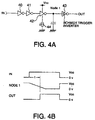
- the delay circuit 5 is structured illustrated in Fig 4A. Specifically, the delay circuit 5 is composed of three inverters 40, 41 and 42, a Schmidt Trigger inverter 43, a constant current supply 44, and a capacitor 45. In this event, a power supply Vcc and the constant current supply 44 are connected to the inverter 42. Further, the capacitor 45 is connected to a Node 1.
- the delay circuit 5 omits a signal which is shorter than a delay time t.
- a signal which has a larger pulse width than the delay time t is outputted at a rise timing which is delayed with the delay time t.
- the latch circuit 6 is put into the L level which is an initial state of the output irrelevant to the signal from the delay circuit 5 when the input signal from the input terminal In is put into the L level.
- the latch circuit 6 becomes a wait state from the delay circuit 5.
- the H level signal is given from the delay circuit 5
- the output of the latch circuit 6 is put into the H level, and thereafter, the H level is kept until the input signal from the input terminal In becomes the L level.
- the input terminal In is put into the L level.
- the latch circuit output point (thereinafter, abbreviated to an E point) is put into the L level.
- the output point (thereinafter, abbreviated to an F point) of the inverter 7 is put into the H level.
- the gate terminal point (thereinafter, abbreviated to a point G) of the output transistor Q1 is put into the L level.
- the output transistor Q1 is turned off.
- the voltage of the point is equal to 0 V because the transistor Q3 is turned off.
- the output (thereinafter, abbreviated to a C point) of the comparator circuit 2 immediately becomes the H level, and soon turns back to the L level.
- the pulse width of this C point is smaller than the delay time t of the delay circuit 5 in the output point (thereinafter, abbreviated to a D point) of the delay circuit 5. Consequently, the voltage of the C point is kept to the L level, and therefore the E point is also kept to the L level.
- the D point is delayed at the delay time t by the delay circuit 5 to become the H level, and the E point is changed into the H level. Therefore, the G point is put into the L level to cut off the output transistor Q1.
- the output transistor Q1 is turned off, the voltage of the point becomes 0V, the C point becomes the L level and the E point is kept to the H level.
- a P-channel MOSFET may be used by giving a negative power supply as the power supply Vcc or the external power supply.
Landscapes
- Electronic Switches (AREA)
- Measurement Of Current Or Voltage (AREA)
Applications Claiming Priority (3)
| Application Number | Priority Date | Filing Date | Title |
|---|---|---|---|
| JP14123997A JP3219019B2 (ja) | 1997-05-30 | 1997-05-30 | 異常電流検出回路およびそれを用いた負荷駆動回路 |
| JP141239/97 | 1997-05-30 | ||
| JP14123997 | 1997-05-30 |
Publications (2)
| Publication Number | Publication Date |
|---|---|
| EP0881769A2 true EP0881769A2 (de) | 1998-12-02 |
| EP0881769A3 EP0881769A3 (de) | 2000-05-17 |
Family
ID=15287343
Family Applications (1)
| Application Number | Title | Priority Date | Filing Date |
|---|---|---|---|
| EP98109653A Withdrawn EP0881769A3 (de) | 1997-05-30 | 1998-05-27 | Überstromdetektor und damit ausgestattete Lasttreiberschaltung |
Country Status (4)
| Country | Link |
|---|---|
| US (1) | US5973551A (de) |
| EP (1) | EP0881769A3 (de) |
| JP (1) | JP3219019B2 (de) |
| KR (1) | KR19980087505A (de) |
Cited By (2)
| Publication number | Priority date | Publication date | Assignee | Title |
|---|---|---|---|---|
| WO2005071511A1 (ja) * | 2004-01-22 | 2005-08-04 | Rohm Co., Ltd | 過電流検出回路及びそれを備えたレギュレータ |
| EP1618444A1 (de) * | 2003-04-16 | 2006-01-25 | Koninklijke Philips Electronics N.V. | Spannungsregelungssystem mit betriebsbedingungsdetektionsmitteln |
Families Citing this family (16)
| Publication number | Priority date | Publication date | Assignee | Title |
|---|---|---|---|---|
| JP4082547B2 (ja) * | 1999-02-26 | 2008-04-30 | 矢崎総業株式会社 | 発光素子の電源供給制御装置 |
| JP3986041B2 (ja) * | 1999-02-26 | 2007-10-03 | 矢崎総業株式会社 | 電源供給制御装置 |
| US6140868A (en) * | 1999-03-09 | 2000-10-31 | Lucent Technologies, Inc. | Master tuning circuit for adjusting a slave transistor to follow a master resistor |
| JP2003264455A (ja) | 2002-03-07 | 2003-09-19 | Matsushita Electric Ind Co Ltd | 出力回路装置 |
| JP2005303969A (ja) * | 2004-03-17 | 2005-10-27 | Nec Electronics Corp | 過電流検出回路 |
| JP4504222B2 (ja) * | 2005-02-21 | 2010-07-14 | 矢崎総業株式会社 | 過電流検出装置 |
| JP2008041884A (ja) * | 2006-08-04 | 2008-02-21 | Rohm Co Ltd | 半導体集積回路およびそれを備えた電子機器 |
| JP2008154419A (ja) * | 2006-12-20 | 2008-07-03 | Ricoh Co Ltd | スイッチングレギュレータ及びスイッチングレギュレータを構成する半導体装置 |
| US7986149B2 (en) * | 2008-08-19 | 2011-07-26 | Infineon Technologies Austria Ag | System and method for adaptive load fault detection |
| US8325453B2 (en) * | 2009-05-28 | 2012-12-04 | Qualcomm, Incorporated | Short-circuit protection for switched output stages |
| JP5537272B2 (ja) * | 2010-06-07 | 2014-07-02 | ローム株式会社 | 負荷駆動回路装置及びこれを用いた電気機器 |
| JP5667946B2 (ja) * | 2011-08-24 | 2015-02-12 | 株式会社東芝 | ハイサイドスイッチ回路 |
| US9024678B2 (en) | 2013-05-22 | 2015-05-05 | Infineon Technologies Ag | Current sensing circuit arrangement for output voltage regulation |
| US9667245B2 (en) * | 2014-10-10 | 2017-05-30 | Efficient Power Conversion Corporation | High voltage zero QRR bootstrap supply |
| JP7391720B2 (ja) * | 2020-03-05 | 2023-12-05 | 株式会社東芝 | 半導体集積回路装置および電流検出回路 |
| US11243264B2 (en) | 2020-04-22 | 2022-02-08 | Renesas Electronics Corporation | Abnormal power supply voltage detection device and method for detecting abnormal power supply voltage |
Citations (6)
| Publication number | Priority date | Publication date | Assignee | Title |
|---|---|---|---|---|
| EP0389832A1 (de) * | 1989-03-28 | 1990-10-03 | STMicroelectronics S.r.l. | Elektronischer Schaltkreis zur Messung und Regelung eines durch eine induktive elektrische Last fliessenden Stromes |
| EP0419093A2 (de) * | 1989-09-20 | 1991-03-27 | Kabushiki Kaisha Toshiba | Strommessschaltung |
| EP0602699A2 (de) * | 1992-12-04 | 1994-06-22 | Koninklijke Philips Electronics N.V. | Leistungshalbleiter mit Strombegrenzung |
| JPH0945849A (ja) * | 1995-07-26 | 1997-02-14 | Nec Corp | 電流検出回路 |
| EP0771072A1 (de) * | 1995-10-25 | 1997-05-02 | Nec Corporation | Eingangsschaltung zum Setzen des Modus |
| EP0814395A2 (de) * | 1996-06-21 | 1997-12-29 | Nec Corporation | Überstrommessungsvorrichtung für Leistungs-MOS-Feldeffekttransistor |
Family Cites Families (4)
| Publication number | Priority date | Publication date | Assignee | Title |
|---|---|---|---|---|
| JPH09191103A (ja) * | 1996-01-09 | 1997-07-22 | Nec Corp | 電流検出手段を有する半導体装置 |
| US5796278A (en) * | 1996-04-26 | 1998-08-18 | Delco Electronics Corporaiton | Circuitry for controlling load current |
| US5892389A (en) * | 1997-06-03 | 1999-04-06 | Motorola, Inc. | Method and circuit for current limiting of DC-DC regulators |
| US5905389A (en) * | 1997-09-22 | 1999-05-18 | Cypress Semiconductor Corp. | Methods, circuits and devices for improving crossover performance and/or monotonicity, and applications of the same in a universal serial bus (USB) low speed output driver |
-
1997
- 1997-05-30 JP JP14123997A patent/JP3219019B2/ja not_active Expired - Fee Related
-
1998
- 1998-05-27 EP EP98109653A patent/EP0881769A3/de not_active Withdrawn
- 1998-05-29 KR KR1019980019735A patent/KR19980087505A/ko not_active Application Discontinuation
- 1998-05-29 US US09/087,636 patent/US5973551A/en not_active Expired - Lifetime
Patent Citations (6)
| Publication number | Priority date | Publication date | Assignee | Title |
|---|---|---|---|---|
| EP0389832A1 (de) * | 1989-03-28 | 1990-10-03 | STMicroelectronics S.r.l. | Elektronischer Schaltkreis zur Messung und Regelung eines durch eine induktive elektrische Last fliessenden Stromes |
| EP0419093A2 (de) * | 1989-09-20 | 1991-03-27 | Kabushiki Kaisha Toshiba | Strommessschaltung |
| EP0602699A2 (de) * | 1992-12-04 | 1994-06-22 | Koninklijke Philips Electronics N.V. | Leistungshalbleiter mit Strombegrenzung |
| JPH0945849A (ja) * | 1995-07-26 | 1997-02-14 | Nec Corp | 電流検出回路 |
| EP0771072A1 (de) * | 1995-10-25 | 1997-05-02 | Nec Corporation | Eingangsschaltung zum Setzen des Modus |
| EP0814395A2 (de) * | 1996-06-21 | 1997-12-29 | Nec Corporation | Überstrommessungsvorrichtung für Leistungs-MOS-Feldeffekttransistor |
Cited By (3)
| Publication number | Priority date | Publication date | Assignee | Title |
|---|---|---|---|---|
| EP1618444A1 (de) * | 2003-04-16 | 2006-01-25 | Koninklijke Philips Electronics N.V. | Spannungsregelungssystem mit betriebsbedingungsdetektionsmitteln |
| WO2005071511A1 (ja) * | 2004-01-22 | 2005-08-04 | Rohm Co., Ltd | 過電流検出回路及びそれを備えたレギュレータ |
| US7573689B2 (en) | 2004-01-22 | 2009-08-11 | Rohm Co., Ltd. | Overcurrent detecting circuit and regulator having the same |
Also Published As
| Publication number | Publication date |
|---|---|
| US5973551A (en) | 1999-10-26 |
| JPH10332751A (ja) | 1998-12-18 |
| EP0881769A3 (de) | 2000-05-17 |
| JP3219019B2 (ja) | 2001-10-15 |
| KR19980087505A (ko) | 1998-12-05 |
Similar Documents
| Publication | Publication Date | Title |
|---|---|---|
| US5973551A (en) | Abnormal current detection circuit and load drive circuit including the same | |
| US7068082B2 (en) | Gate driving circuit and semiconductor device | |
| US7405916B2 (en) | Control apparatus of semiconductor switch | |
| US7622874B2 (en) | Over current detection circuits for motor driver | |
| EP0497319B1 (de) | Integrierte Halbleiter-Schaltungseinheit mit Detektionsschaltung für Substrat-Potential | |
| US6351360B1 (en) | Apparatus for selective shutdown of devices of an integrated circuit in response to thermal fault detection | |
| JP3637848B2 (ja) | 負荷駆動回路 | |
| US7359171B2 (en) | Current limiting circuit and output circuit including the same | |
| US6346834B1 (en) | Power on reset circuit | |
| US6369556B2 (en) | Power supply control device and method | |
| US20030107422A1 (en) | Latch circuit | |
| US5696658A (en) | Short circuit protection circuit for a low-side driver circuit | |
| EP0746905A1 (de) | Ein halbleiter-leistungsschalter | |
| US6891708B2 (en) | Reduced current and power consumption structure of drive circuit | |
| US7724047B2 (en) | Semiconductor integrated circuit driving external FET and power supply incorporating the same | |
| CN115856411A (zh) | 功率驱动管及其过流检测电路及过流检测方法 | |
| US5550486A (en) | Circuit and method for providing a known logic state at insufficient supply voltage | |
| US6943596B2 (en) | Power-on reset circuit for use in low power supply voltage applications | |
| JP2004525552A (ja) | 3端子非反転トランジスタスイッチ | |
| JP3596415B2 (ja) | 誘導性負荷駆動回路 | |
| JPH118928A (ja) | 短絡防止回路 | |
| JP3331601B2 (ja) | 負荷状態検出回路 | |
| JP3909542B2 (ja) | 電圧検出装置 | |
| JPH1127845A (ja) | 過電流防止回路 | |
| US6614637B1 (en) | Apparatus and method for a discharge interrupt circuit that can operate at a low supply voltage |
Legal Events
| Date | Code | Title | Description |
|---|---|---|---|
| PUAI | Public reference made under article 153(3) epc to a published international application that has entered the european phase |
Free format text: ORIGINAL CODE: 0009012 |
|
| AK | Designated contracting states |
Kind code of ref document: A2 Designated state(s): DE FR |
|
| AX | Request for extension of the european patent |
Free format text: AL;LT;LV;MK;RO;SI |
|
| PUAL | Search report despatched |
Free format text: ORIGINAL CODE: 0009013 |
|
| AK | Designated contracting states |
Kind code of ref document: A3 Designated state(s): AT BE CH CY DE DK ES FI FR GB GR IE IT LI LU MC NL PT SE |
|
| AX | Request for extension of the european patent |
Free format text: AL;LT;LV;MK;RO;SI |
|
| 17P | Request for examination filed |
Effective date: 20000828 |
|
| AKX | Designation fees paid |
Free format text: DE FR |
|
| 17Q | First examination report despatched |
Effective date: 20010716 |
|
| STAA | Information on the status of an ep patent application or granted ep patent |
Free format text: STATUS: THE APPLICATION HAS BEEN WITHDRAWN |
|
| 18W | Application withdrawn |
Withdrawal date: 20010918 |