EP0764985B1 - Getarnter digitaler Schaltkreis mit Transistorgeometrie und Kanalunterbrechungen und Herstellungsverfahren desselben - Google Patents
Getarnter digitaler Schaltkreis mit Transistorgeometrie und Kanalunterbrechungen und Herstellungsverfahren desselben Download PDFInfo
- Publication number
- EP0764985B1 EP0764985B1 EP96107428A EP96107428A EP0764985B1 EP 0764985 B1 EP0764985 B1 EP 0764985B1 EP 96107428 A EP96107428 A EP 96107428A EP 96107428 A EP96107428 A EP 96107428A EP 0764985 B1 EP0764985 B1 EP 0764985B1
- Authority
- EP
- European Patent Office
- Prior art keywords
- transistors
- interconnections
- taps
- channel
- cells
- Prior art date
- Legal status (The legal status is an assumption and is not a legal conclusion. Google has not performed a legal analysis and makes no representation as to the accuracy of the status listed.)
- Expired - Lifetime
Links
Images


Classifications
-
- H—ELECTRICITY
- H10—SEMICONDUCTOR DEVICES; ELECTRIC SOLID-STATE DEVICES NOT OTHERWISE PROVIDED FOR
- H10W—GENERIC PACKAGES, INTERCONNECTIONS, CONNECTORS OR OTHER CONSTRUCTIONAL DETAILS OF DEVICES COVERED BY CLASS H10
- H10W42/00—Arrangements for protection of devices
- H10W42/40—Arrangements for protection of devices protecting against tampering, e.g. unauthorised inspection or reverse engineering
-
- G—PHYSICS
- G11—INFORMATION STORAGE
- G11C—STATIC STORES
- G11C7/00—Arrangements for writing information into, or reading information out from, a digital store
- G11C7/24—Memory cell safety or protection circuits, e.g. arrangements for preventing inadvertent reading or writing; Status cells; Test cells
-
- H—ELECTRICITY
- H10—SEMICONDUCTOR DEVICES; ELECTRIC SOLID-STATE DEVICES NOT OTHERWISE PROVIDED FOR
- H10D—INORGANIC ELECTRIC SEMICONDUCTOR DEVICES
- H10D89/00—Aspects of integrated devices not covered by groups H10D84/00 - H10D88/00
Definitions
- the invention relates to a camouflaged digital integrated circuit (IC) according to the preamble of claim 1, and to a method of fabricating such an IC, according to the preamble of claim 7.
- IC camouflaged digital integrated circuit
- This invention relates, in general, to the prevention of reverse engineering of integrated circuits (ICs), and more particularly to security techniques in which a common geometric design is established for different circuit cells and interconnections between circuit elements are made undetectable.
- SEM scanning electron microscope
- SIMS secondary ion mass spectrometry
- a general description of e-beam probing is provided in Lee, Engineering a Device for Electron-beam Probing:, IEEE Design & Test of Computers, 1989, pages 36-49 .
- US-Patent No. 4,799,096 to Koeppe uses doped implants to connect the sources and drains of different transistors to improve circuit reliability and testability, but the circuit function can be determined from the transistor arrangement.
- US-Patent No. 5,138,197 to Kuwana connects different transistors in an address decoder array with doped implants, but circuit functions can be determined from clearly visible elements such as gate electrodes and circuit interconnects.
- Japanese patent publication 58-190064 to Sawase provides a metalization over a diffused source to block light from the source/substrate junction and thus reduce leakage current. While this tends to camouflage the source, the nature of the circuit can still be determined from its visible elements.
- a semiconductor device wherein when adjacent P + -diffused wirings are connected to each other, a channel stopper (boron B), for example, is ion-implanted between the wirings to form a channel stopper implanted region and the wirings are electrically connected through this region.
- boron B boron B
- the formation of the region can be performed at the same time as the time of a channel stop region formation process and a well formation process, which are a normal process.
- the region cannot be read by simply observing and analyzing its surface configuration. Thereby, the prevention of a dead copy can be contrived without complicating a manufacturing process.
- a transistor in an integrated circuit is known, wherein the doping of a portion thereof serves as a short circuit or an interruption between source and drain.
- the present invention is related to a camouflage digital integrated circuit, wherein said pattern of interconnections is a uniform pattern of electrically conductive implant interconnections among said transistors, wherein at least some of said interconnections in said uniform pattern of interconnections are apparent interconnections realized by interrupting said interconnections by means of implanted channel stops of opposite conductivity than the interconnections and said apparent interconnections are used so as to organize said transistors into logic cells with different logic functions.
- the present invention seeks to provide a camouflaged digital IC, and a fabrication method for the IC, that is very difficult to reverse engineer, can be implemented without any additional fabrication steps and is compatible with computer aided design (CAD) systems that allow many different kinds of logic circuits to be constructed with ease.
- CAD computer aided design
- the size and internal geometry of the transistors within each of the cells are made the same for the same transistor type, different logic cells have their transistors arranged in substantially the same spatial pattern so that the logic functions are not discernable from the transistor patterns, and the transistors are collectively arranged in a uniform array on the substrate so that boundaries between different logic cells are similarly not discernable.
- a uniform pattern of interconnections among all of the transistors on the substrate is preferably provided, with different logic functions implemented by interrupting some of the interconnections to make them apparent (they appear to be conductive connections but are actually non-conductive) by the addition of opposite conductivity channel stop implants.
- the channel stops are substantially shorter than the interconnections which they interrupt, preferably with a dimension equal approximately to the minimum feature size of the IC. To the extent the interconnections could be discerned by a reverse engineer, they would all look the same because the channel stops would not be detected, thus enhancing the circuit camouflage.
- Reverse engineering is further inhibited by providing a uniform pattern of metal leads over the transistor array.
- a uniform pattern of heavily doped implant taps are made to the various transistors to connect with the leads. Some of the taps are made apparent by blocking them with channel stops similar to those employed in the apparent inter-transistor connections. A reverse engineer will thus be unable to either determine boundaries between different cells, or to identify different cell types, from either the metalization or the tap patterns.
- the metalization is preferably implemented in multiple layers, with the upper layers shading connections between a lower layer and the underlying IC.
- a camouflaged circuit is preferably fabricated by implanting the interconnections and the portions of the transistors which have the same conductivity at the same time, and also implanting the channel stops and the portions of the transistors which have the same conductivity as the channel stops at the same time.
- the invention camouflages digital logic cells by arranging all of the transistors for each of the cells in a uniform "sea" of transistors in which the boundaries between different cells are not apparent, by arranging the transistors within different cells that have the same number of transistors but different logic functions in the same geometric layout so that the cell functions cannot be determined by the transistor geometries, by using implants that are made electrically conductive by heavy doping and are not readily discernable for intracell connections, and by providing the same geometric layout of intracell interconnections for different logic cells so that the cell functions cannet be determined even if the interconnections are determined by a reverse engineer.
- a uniform pattern of interconnections is achieved by providing implants for all potential interconnections within each cell, and disabling unwanted interconnections for a given cell with narrow implanted channel stops of opposite conductivity. Since the channel stops are even more difficult to discern than are the implanted interconnections, a still higher level of protection is provided. Heavily doped implants with a common geometric layout and channel stop interruptions can also be used for intercell as well as intracell connections.
- Reverse engineers typically attempt to recognize transistor patterns and interconnections that correspond to different logic cells, and then try to identify similar patterns throughout the logic array. This saves the effort of having to investigate each transistor individually. Interconnections between cells are determined by photographing the metalization layers and superimposing them on the cells. The use of repetitive cell patterns greatly simplifies the reverse engineer's task. For example, for an array of 100,000 cells that employs 100 different types of cells, the reverse engineer only has to identify 100 different cell types. The present invention forces a reverse engineer to investigate each individual transistor within each cell, and even then the overall circuit is extremely difficult to reconstruct.
- An important aspect of the invention is that it does not rely upon modifications or additions to the functioning of the circuitry that is to be protected from reverse engineering, nor does it require any additional processing steps or equipment. Instead, a highly effective deterrent to reverse engineering is accomplished in a streamlined manner that adds neither processing, time nor complexity to the basic circuitry.
- Implementations of the invention in the form of OR and AND gates will first be described. Using these and other common gates as building blocks, many different types of logic circuitry can be designed. A distinct advantage of the invention is that different types of logic circuits may be made to look alike, thus confusing a potential reverse engineer.
- FIG. 1 is a schematic diagram of a conventional three-input OR gate circuit, in which three p-channel transistors 2, 4 and 6 are connected in series between a positive voltage terminal 8 and an inverted output 10, and three n-channel transistors 12, 14 and 16 are connected in parallel between a negative voltage terminal 18 (which can be designated ground) and the inverted output 10.
- Input terminals 20, 22 and 24 for the inputs designated A, B and C are connected to the gates of respective p-channel/n-channel transistor pairs.
- the signal at inverted output 10 represents a NOR function.
- an inverter 26 inverts the signal at output 10 to produce an OR output at terminal 28.
- the inverter is conventional, consisting of a p-channel transistor 30 and an n-channel transistor 32 that are connected in series between the positive and negative voltage terminals 8 and 18, with the gates of transistors 30 and 32 receiving an input from inverted output 10 and output terminal 28 tapped from the series junction of 30 and 32.
- FIG. 2 A conventional three-input AND gate is illustrated in FIG. 2 . It is similar to the OR gate of FIG. 1 , but for the AND gate the three p-channel transistors 2', 4' and 6' are connected in parallel, and the three n-channel transistors 12', 14' and 16' are connected in series. Again, an inverted function (NAND) is produced at an inverted output 10', and inverted to yield the desired AND signal at the final output terminal 28'.
- NAND inverted function
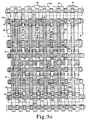
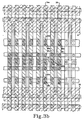
- FIGs. 3a and 3b are plan views of the same area in a logic array, with FIG. 3a emphasizing the transistor drain, source and interconnection implants by shading them from lower left to upper right (polysilicon gates are shaded from upper left to lower right), and FIG. 3b emphasizing the metalization that overlies the IC substrate.
- FIG. 3b the lower level of metalization (metal-1) which directly contacts the underlying IC is shaded from lower left to upper right, while the upper metal-2 metalization that interconnects different portions of the metal-1 is shaded from upper left to lower right.
- Metal-1 is shown in dashed lines and metal-2 in solid but unshaded lines in FIG. 3a .
- Contact connections between the IC and the metal-1 layer are indicated by hollow squares M1, while vertical conductive vias which substitute connections between the metal-1 and metal-2 layers for the IC-metal-1 contacts are stipled and labeled M2.
- the sources, drains and gates of each of the transistors are indicated by the same transistor numbers as in FIG. 1 , followed by S, D or G, respectively.
- the transistor sources and drains (the designation of an element as a source or a drain is somewhat arbitrary) are fabricated in a conventional manner by implanting dopant ions into the circuit substrate. While both the p+ and n+ doping can vary with parameters such as feature size and the type of fabrication process used, the p+ sources and drains of the p-channel devices 2, 4, 6 and 30 are typically doped with a boron ion implant at a density of about 4 ⁇ 10 15 ion/ cm 2 , and an implantation energy of about 30 keV.
- n+ source and drain regions of the n-channel transistors 12, 14, 16 and 32 are typically doped in accordance with industry standards with arsenic ions at a density of about 5 ⁇ 10 15 /cm 2 , and an implant energy of about 150 keV. Either a masked ion flood beam or a focused ion beam may be used; doping by older gaseous diffusion techniques may also be employed.
- FIG. 3a the transistors used in the OR gate of FIG. 1 are shaded for clarity, while the remaining transistors are unshaded. All of the p-channel transistors in the entire array have substantially the same sizes and geometric layouts; the n-channel transistors similarly have the same size and geometric layout. This is of considerable benefit in camouflaging the cell to which a particular transistor belongs, and also the boundaries between cells, since normally different cell transistors of the same conductivity type will not all have the same size. For example, output transistors are normally larger because they carry more current. This can be accommodated by the invention by making all of the transistors somewhat larger, although at the price of a greater overall area and consequently some degradation in the device density.
- buffer circuits could be employed to boost the output currents if the output transistors are reduced to the size of the other transistors, or the ratio of the source/drain width W (in the vertical direction in FIG. 3a ) to the gate length L (the narrow horizontal gate dimension in FIG. 3a ) can be increased.
- the W/L ratio is conventionally about 7-15 for an n-channel device, and about 15-30 for p-channel device. This ratio can be increased on the order of about 15% to accommodate the invention.
- Another consequence of using equal size transistors is that the circuit's operating speed can go down somewhat because of extra parasitic capacitances, although the transistors can be used in parallel to obtain more output drive. Since the camouflaged cells tend to be larger and slower than conventional cells, it may be desirable to implement only the more important portion of a complete circuit on a single die with the invention's camouflage techniques, with the remainder of the circuit implemented using conventional cells.
- the camouflage provided by the invention is considerably enhanced by a transistor interconnection scheme that greatly adds to the difficulty of reverse engineering.
- Such connections are made by means of doping implants into the substrate between the desired sources and drains.
- Such interconnections are preferably implemented, as shown in FIG. 3a , by extending the source and drain implants on either side of the transistors with taps that are labeled ST for source taps and DT for drain taps, and by connectors C that interconnect the source and drain taps for the same transistor and the sources and drains of adjacent transistors.
- the implanted interconnections are preferably established simultaneously with the source and drain implants by providing appropriate openings in the implantation mask (if flood beam implantation is employed), or by extending the scanning area of a focused ion beam.
- An alternate method of implantation would be a conventional gaseous diffusion process to establish the doping, but this is less preferable than ion beams.
- the interconnections have the same dopant concentration as the sources and drains and are formed integrally therewith.
- a uniform pattern of interconnections is provided for the transistors of each cell; the pattern includes all of the interconnections that could be used for any of the different cells in the overall IC.
- both intra- and intertransistor connectors C1 and C2, respectively, are implanted at the opposite extremities of the source and drain taps ST and DT
- intertransistor connectors C3 are provided between the inner ends of the sources and drains of adjacent transistors
- intertransistor connectors C4 are provided between the inner extremities of the source and drain taps ST and DT of adjacent transistors.
- Logic functionality is established by interrupting selected taps and connectors with channel stop implants, with the remaining uninterrupted taps and connectors determining the cell functionality.
- the channel stops are of opposite conductivity to the interconnections which they respectively interrupt, and are preferably implanted in the same fabrication step as the other portions of the circuit that have the same conductivity as the channel stop.
- the channel stops are preferably made as small as possible, consistent with providing a secure interruption of the interconnections in which they are located. This will generally be the minimum feature size of the IC, which with present generally available technology is 0.5 microns. If the channel stops were confined to the widths of the interconnections which they interrupt and had upper surfaces planar with these interconnections, they would be totally invisible to presently available reverse engineering techniques. On the other hand, the channel stops will normally extend slightly beyond the limits of their respective interconnections to assure a reliable interruption. Also, since n+ and p+ doping normally exhibit different etch rates, the surface of the IC from one side of a channel stop to the opposite side will normally not be absolutely planar.
- the preferred channel stop dimension of about 0.5 microns approximates the wavelength of visible light, which would make the channel stops invisible to observation in this wavelength regime. Furthermore, with a very narrow channel stop the normal lateral spreading of the faster n+ etching would tend to reduce or even entirely eliminate the surface differential that would otherwise accompany the different etch rates, making reverse engineering even more difficult.
- the channel stops CSO that are implanted to implement the OR gate are stipled, while potential channel stop sites CS1 that are not used for this particular logic cell, leaving their respective interconnects uninterrupted, are shown in outline only. The correspondence between FIGs. 1 and 3a is readily apparent.
- the metal-1 lead 8 provides a Vdd power input in FIG. 3a
- the metal-1 lead 18 provides a Vss (ground) source.
- the series connection from Vdd 8 through p-channel transistors 2, 4 and 6 to the NOR output terminal 10 extends from the M1 lead 8 to the upper end of the source tap ST for the source 2S of transistor 2 and through an unblocked channel stop site to 2S; from the lower end of 2D through a connector C3 to 4S; from the lower end of 4D through another connector C3 to the lower end of 6S; through an unblocked channel stop site at the lower end of 6D and another unblocked channel stop site in a connector C4 to a blocked tap at the lower end of 30S; and up through a contact M1a in the blocked tap to a metal-1 link which serves as the NOR output node 10 (shown in FIG. 3b ).
- the inverter transistors 30 and 32 are shown on the right side of the shaded area of FIG. 3a .
- the gate input to p-channel transistor 30 from NOR output node 10 is through the metal-1 contact M1b, while the OR output 28 is taken from the metal-1 contact M1c at the tap from the lower end of 30D, and up through the via M2a to the metal-2 line 28 (shown in FIG. 3b ).
- connection from the NOR output 10 to the n-channel transistors 12, 14 and 16 extends from the lower end of 6D, through a contact M1d to the metal-1 layer; a via M2b that is linked by metal-1 to M1d and extends up to a metal-2 line 34a; and down 34a and through another via M2c to a metal-1 link which connects it to a metal-1 contact M1e at the upper end of 16D.
- the pattern of unblocked and blocked channel stop sites in the n-channel portion of the cell establishes the parallel connection of n-channel transistors 12, 14 and 16, with a connection of 12S to ground line 18 through an unblocked metal-1 contact from a tap ST at the lower end of 12S.
- the rows of p-channel and n-channel transistors extend in a horizontal direction over the full extent of the IC transistor array, without any visibly discernable distinctions between the transistors of the same conductivity within a given cell or among different cells.
- the vertical columns of alternating p-channel and n-channel transistors extend over the full IC transistor array, again with all of the p-channel transistors in each column having the same size and geometric layout, and the same for all the n-channel transistors.
- FIGs. 3a and 3b The OR cell illustrated in FIGs. 3a and 3b is shown with channel stops that isolate it from adjacent logic cells to both the left and right. Interconnections with such cells can be made if desired by metal-1 connections and/or eliminating selected channel stops. Interconnections between different logic cells within a vertical column would normally be made through the metal-2 leads.
- the AND gate shown in FIG. 2 would be implemented in a manner similar to FIGs. 3a and 3b , but the connections for the p-channel and n-channel transistors would be reversed from those shown in FIGs. 3a and 3b .
- Many other cells with varying numbers of n-channel/p-channel transistor pairs could be stored in a library for use with a CAD system.
- such cells could include NOR and NAND gates with different numbers of inputs, exclusive or (XOR) gates, all with or without output inverters, multiplexers, various types of flip-flops and combinations of different logic functions.
- the metalization patterns are uniform and repetitive.
- the dimensions of and spacings between metallizations is uniform whenever possible. This is contrary to conventional circuit layouts, in which non-uniform spacings are used to minimize parasitic capacitances. While this aspect of the invention can degrade performance somewhat, particularly because it can conflict with an optimal geometric positioning of the Vdd and ground lines to minimize parasitic capacitances, the reduction in operating speed is more than offset by the enhanced camouflage effect for high security applications. Again, the uniform pattern makes it much more difficult to discern cell boundaries and functions.
- metal lines are preferably run all the way across each cell in their path, rather than terminating at a target location within a cell such as the gate contact.
- the polysilicon gates (assuming a silicon substrate is used) can be formed either before or after the source, drain, interconnect and channel stop implants.
- the metal-1 and metal-2 connectors and their respective contacts and vias are of course formed over the completed IC.
- FIGs. 4a and 4b are sectional views (not to scale) taken along the section lines 4a-4a and 4b-4b of FIG. 3a , illustrating the fabrication of their respective source, drain, interconnection and channel stop implants, but excluding the polysilicon and metalization layers.
- the devices are formed in a semiconductor substrate 38 that for illustrative purposes is silicon, but may also be GaAs, some other desired semiconductor material, or in principle any nonconductive material such as silicon-on-sapphire.
- circuit fabrication can be accomplished with a conventional process, such as that described in Frederiksen, Intuitive CMOS Electronics, McGraw-Hill Publishing Co., 1989, pages 134-145 ; it is a distinct advantage of the invention that it does not require any special processing to implement.
- a protective oxide layer about 250 Angstroms thick is first laid down over the semiconductor substrate 38.
- a well is then implanted through openings in the oxide layer for each FET whose source and drain is of the same conductivity type as the substrate doping.
- substrate 38 illustrated as having an n- doping a somewhat more heavily doped p-well 40 would be implanted about 3 microns deep for the n-channel devices ( FIG. 4a ).
- the wells are then subjected to a long high temperature anneal, typically at about 1,150° C, for about 10 hours.
- the next step is the FET source, drain and interconnection implants.
- an oxide mask 42 is laid down over the substrate with openings at the desired locations for the sources and drains.
- a single continuous mask opening 44 is provided to implant the drain 12D, the source 12S, the outer and inner source and drain taps ST and DT, and the connector C1.
- the implantation is then performed, preferably with a flood beam (indicated by numeral 46) of suitable n-dopant ions such as arsenic.
- the unused channel stop sites CS1 are left with the same doping conductivity as their respective taps and connectors, while the active channel stops CSO are implanted to the opposite conductivity. This can be done by providing a mask over the CSO sites during the implantation of the source and drain and implanting the channel stops during the implantation of the p-channel transistors, or by implanting the channel stops n+ along with the rest of the n-channel transistors and then (or previously) performing a double-dose p+ implant that is restricted to the channel stops.
- a separate implant mask 48 is used for the p-channel devices ( FIG. 4b ).
- a single continuous opening 50 is provided in the mask for the taps and connectors and the transistor elements which they connect; these are illustrated as p-channel FET source 2S, drain 2D, drain taps DT, source taps ST and connector C1.
- Implantation is preferably performed with a flood beam, indicated by numeral 52, of a suitable p-type dopant such as boron.
- the implantation can be performed in the same manner as prior unsecured processes, the only difference being that the implant is now done through a larger opening in each mask that includes the implanted taps and connectors as well as the FET sources and drains, but excludes the channel stops. No differences in processing time or techniques are required, and the operator need not even know that the mask provides for circuit security.
- the circuits are then completed in a conventional manner, with threshold implants made into the FET channels to set the transistor characteristics.
- a field oxide is laid down as usual, and polysilicon is then deposited and doped either by diffusion or ion implantation to form the channels and the interconnects.
- a dielectric is next deposited and metalization layers added to establish inputs, outputs, bias line and any necessary cell linkages. Finally, an overglass or other suitable dielectric coating is laid down over the entire chip.
- an integrated digital circuit is protected from reverse engineering by fabricating all transistors of like conductivity 2, 4, 6, 30; 12, 14, 16, 32 with a common size and geometric layout, providing a common layout for different logic cells, connecting doped circuit elements of like conductivity with electrically conductive doped implants C in the substrate 38 rather than metalized interconnections, and providing non-functional apparent interconnections that are interrupted by non-discernable channel stops CSO so that all cells falsely appear to have a common interconnection scheme.
- the camouflage is enhanced by providing a uniform pattern of metal leads 8, 18, 28, 34 over the transistor array, with a uniform pattern of heavily doped implant taps ST, DT from the transistors for connection to the leads; undesired tap-lead connections are blocked by channel stops.
Landscapes
- Design And Manufacture Of Integrated Circuits (AREA)
- Semiconductor Integrated Circuits (AREA)
- Metal-Oxide And Bipolar Metal-Oxide Semiconductor Integrated Circuits (AREA)
- Storage Device Security (AREA)
- Internal Circuitry In Semiconductor Integrated Circuit Devices (AREA)
Claims (9)
- Getarnte digitale integrierte Schaltung (IC) mit:einem Substrat (38),einem Array von Logikzellen (2, 4, 6, 12, 14, 16, 30, 32) aus mehreren Transistoren der integrierten Schaltung auf dem Substrat (38), wobei die Logikzellen eine Mehrzahl von entsprechenden Logikfunktionen aufweisen, wobei die Transistoren (2 - 6, 12 - 16, 30, 32) der Logikzellen in einem gemeinsamen räumlichen Muster angeordnet sind, so dass ihre entsprechenden Logikfunktionen aus ihren Transistormustern nicht erkennbar sind,elektrisch leitenden implantierten Verbindungen (C) zwischen den Transistoren (2 - 6, 12 - 16, 30, 32) innerhalb jeder Zelle, wobei das Muster der Verbindungen (C) innerhalb jeder Zelle ihre logische Funktion bestimmt, undexternen Anschlüssen (8, 18, 28, 34) zu den Zellen,dadurch gekennzeichnet, dass das Muster der Verbindungen (C) ein einheitliches Muster von elektrisch leitenden implantierten Verbindungen (C) zwischen den Transistoren (2 - 6, 12-16, 30, 32) ist, wobei wenigstens einige der Verbindungen (C) in dem einheitlichen Muster von Verbindungen (C) scheinbare Verbindungen (C) sind, die durch implantierte Kanalunterbrechungen entgegengesetzter Leitfähigkeit als die Verbindungen (C) realisiert sind und die scheinbaren Verbindungen (C) dazu verwendet werden, um die Transistoren (2 - 6, 12 - 16, 30, 32) in Logikzellen mit unterschiedlichen logischen Funktionen zusammenzuschalten.
- Getarnte digitale integrierte Schaltung nach Anspruch 1, dadurch gekennzeichnet, dass jeder der Transistoren desselben Leitfähigkeitstyps (2, 4, 6, 30; 12, 14, 16, 32) in jeder der Zellen eine gemeinsame Größe aufweist.
- Getarnte digitale integrierte Schaltung nach Anspruch 1 oder 2, dadurch gekennzeichnet, dass die externen Anschlüsse durch ein einheitliches Muster von metallischen Leitungen (8, 18, 28, 34), die über dem Zellenarray liegen, bereitgestellt sind.
- Getarnte digitale integrierte Schaltung nach einem der Ansprüche 1 bis 3, dadurch gekennzeichnet, dass
das Array von Transistoren (2 - 6, 12 - 16, 30, 32) ein einheitliches Array von IC-Transistoren (2, 4, 6, 12, 14, 16, 30, 32) auf dem Substrat (38) ist. - Getarnte digitale integrierte Schaltung nach einem der Ansprüche 1 bis 4, gekennzeichnet durch ein einheitliches Muster von metallischen Leitungen (8, 18, 28, 34), die über dem Transistorarray liegen und externe Anschlüsse zu wenigstens einigen der Transistoren (2 - 6, 12 - 16, 30, 32) bereitstellen.
- Getarnte digitale integrierte Schaltung nach Anspruch 1, gekennzeichnet durch ein einheitliches Muster von elektrisch leitenden implantierten Abgriffen (ST, DT) der Transistoren (2 - 6, 12 - 16, 30, 32) und metallischen Verbindungen (M1) zwischen den Abgriffen (ST, DT) und den Leitungen (8, 18, 28, 34), wobei wenigstens einige der Abgriffe (ST, DT) mit einer Kanalunterbrechung ausgebildet sind, die die entgegengesetzte Leitfähigkeit der elektrischen Leitfähigkeit der implantierten Abgriffe (ST, DT) aufweist.
- Verfahren zur Herstellung einer getarnten digitalen integrierten Schaltung (IC) mit den Schritten:Implantieren eines Arrays von Transistoren (2, 4, 6, 12, 14, 16, 30, 32) in einem Substrat (38),Implantieren von gemeinsamen Mustern von elektrisch leitenden dotierten Verbindungen (C) zwischen den Transistoren (2 - 6, 12 - 16, 30, 32), undAnordnen der Transistoren (2 - 6, 12 - 16, 30, 32) der Logikzellen in einem einheitlichen Array von IC-Transistoren (2 - 6, 12 - 16, 30, 32) auf dem Substrat (38), so dass Grenzen zwischen unterschiedlichen logischen Zellen in gleicher Weise nicht erkennbar sind,Verwenden von Transistoren (2-6, 12-16, 30, 32) desselben Leitfähigkeitstyps in jeder der Logikzellen, wobei die Transistoren (2 - 6, 12 - 16, 30, 32) eine gemeinsame Größe aufweisen,gekennzeichnet durch die weiteren Schritte
Bereitstellen einiger Verbindungen (C) mit einer Kanalunterbrechung entgegengesetzter Leitfähigkeit als die Verbindung (C), so dass sie leitend erscheinen, aber tatsächlich nicht leitend sind, um unterschiedliche logische Funktionen für unterschiedliche Gruppen von Transistoren (2-6, 12-16, 30, 32), die gemeinsame Transistorgrößen und Layouts aufweisen, zu implementieren. - Verfahren nach Anspruch 7, dadurch gekennzeichnet, dass die unterbrochenen Verbindungen (C) durch Implantieren hochdotierter Kanalunterbrechungen (CSO) entgegengesetzter Leitfähigkeit in die Verbindung hinein unterbrochen sind.
- Verfahren nach Anspruch 8, gekennzeichnet durch die Schritte des Implantierens elektrisch leitender dotierter Abgriffe (DT, ST) von wenigstens einigen der Transistoren (2 - 6, 12 - 16, 30, 32) zum Aufnehmen externer Anschlüsse, des Unterbrechens wenigstens einiger der Abgriffe (ST, DT) mittels einer Kanalunterbrechung, die die entgegengesetzte Leitfähigkeit des dotierten Abgriffs (ST, DT) aufweist, und des Bereitstellens externer Anschlüsse zu den Abgriffen (DT, ST).
Applications Claiming Priority (2)
| Application Number | Priority Date | Filing Date | Title |
|---|---|---|---|
| US532326 | 1995-09-22 | ||
| US08/532,326 US5783846A (en) | 1995-09-22 | 1995-09-22 | Digital circuit with transistor geometry and channel stops providing camouflage against reverse engineering |
Publications (3)
| Publication Number | Publication Date |
|---|---|
| EP0764985A2 EP0764985A2 (de) | 1997-03-26 |
| EP0764985A3 EP0764985A3 (de) | 1999-11-17 |
| EP0764985B1 true EP0764985B1 (de) | 2009-09-30 |
Family
ID=24121317
Family Applications (1)
| Application Number | Title | Priority Date | Filing Date |
|---|---|---|---|
| EP96107428A Expired - Lifetime EP0764985B1 (de) | 1995-09-22 | 1996-05-10 | Getarnter digitaler Schaltkreis mit Transistorgeometrie und Kanalunterbrechungen und Herstellungsverfahren desselben |
Country Status (4)
| Country | Link |
|---|---|
| US (3) | US5783846A (de) |
| EP (1) | EP0764985B1 (de) |
| JP (1) | JP3172672B2 (de) |
| DE (1) | DE69638040D1 (de) |
Cited By (2)
| Publication number | Priority date | Publication date | Assignee | Title |
|---|---|---|---|---|
| US8168487B2 (en) | 2006-09-28 | 2012-05-01 | Hrl Laboratories, Llc | Programmable connection and isolation of active regions in an integrated circuit using ambiguous features to confuse a reverse engineer |
| US8524553B2 (en) | 2002-12-13 | 2013-09-03 | Hrl Laboratories, Llc | Integrated circuit modification using well implants |
Families Citing this family (68)
| Publication number | Priority date | Publication date | Assignee | Title |
|---|---|---|---|---|
| EP0585601B1 (de) | 1992-07-31 | 1999-04-28 | Hughes Electronics Corporation | Sicherheitssystem für integrierte Schaltung und Verfahren mit implantierten Leitungen |
| US5783846A (en) * | 1995-09-22 | 1998-07-21 | Hughes Electronics Corporation | Digital circuit with transistor geometry and channel stops providing camouflage against reverse engineering |
| US5973375A (en) * | 1997-06-06 | 1999-10-26 | Hughes Electronics Corporation | Camouflaged circuit structure with step implants |
| US6173436B1 (en) * | 1997-10-24 | 2001-01-09 | Vlsi Technology, Inc. | Standard cell power-on-reset circuit |
| JP3523521B2 (ja) * | 1998-04-09 | 2004-04-26 | 松下電器産業株式会社 | Mosトランジスタ対装置 |
| DE59813938D1 (de) * | 1998-08-19 | 2007-04-19 | Infineon Technologies Ag | Halbleiterchip mit Oberflächenabdeckung gegen optische Untersuchung der Schaltungsstruktur |
| DE19852072C2 (de) | 1998-11-11 | 2001-10-18 | Infineon Technologies Ag | Verfahren zur Herstellung eines Halbleiterbauelements mit einer stückweise im Substrat verlaufenden Verdrahtung |
| WO2000031871A1 (en) * | 1998-11-25 | 2000-06-02 | Nanopower, Inc. | Improved flip-flops and other logic circuits and techniques for improving layouts of integrated circuits |
| US6117762A (en) * | 1999-04-23 | 2000-09-12 | Hrl Laboratories, Llc | Method and apparatus using silicide layer for protecting integrated circuits from reverse engineering |
| US6396368B1 (en) | 1999-11-10 | 2002-05-28 | Hrl Laboratories, Llc | CMOS-compatible MEM switches and method of making |
| US7217977B2 (en) | 2004-04-19 | 2007-05-15 | Hrl Laboratories, Llc | Covert transformation of transistor properties as a circuit protection method |
| EP1193758A1 (de) | 2000-10-02 | 2002-04-03 | STMicroelectronics S.r.l. | Entschlüsselung erschwerende Kontakte |
| US6815816B1 (en) * | 2000-10-25 | 2004-11-09 | Hrl Laboratories, Llc | Implanted hidden interconnections in a semiconductor device for preventing reverse engineering |
| DE10058078C1 (de) * | 2000-11-23 | 2002-04-11 | Infineon Technologies Ag | Integrierte Schaltungsanordnung mit Analysierschutz und Verfahren zur Herstellung der Anordnung |
| US6791191B2 (en) | 2001-01-24 | 2004-09-14 | Hrl Laboratories, Llc | Integrated circuits protected against reverse engineering and method for fabricating the same using vias without metal terminations |
| US7294935B2 (en) * | 2001-01-24 | 2007-11-13 | Hrl Laboratories, Llc | Integrated circuits protected against reverse engineering and method for fabricating the same using an apparent metal contact line terminating on field oxide |
| US6965375B1 (en) * | 2001-04-27 | 2005-11-15 | Palm, Inc. | Compact integrated touch panel display for a handheld device |
| US6459629B1 (en) * | 2001-05-03 | 2002-10-01 | Hrl Laboratories, Llc | Memory with a bit line block and/or a word line block for preventing reverse engineering |
| US6774413B2 (en) | 2001-06-15 | 2004-08-10 | Hrl Laboratories, Llc | Integrated circuit structure with programmable connector/isolator |
| US6740942B2 (en) | 2001-06-15 | 2004-05-25 | Hrl Laboratories, Llc. | Permanently on transistor implemented using a double polysilicon layer CMOS process with buried contact |
| US6703641B2 (en) * | 2001-11-16 | 2004-03-09 | International Business Machines Corporation | Structure for detecting charging effects in device processing |
| US6897535B2 (en) * | 2002-05-14 | 2005-05-24 | Hrl Laboratories, Llc | Integrated circuit with reverse engineering protection |
| US7049667B2 (en) * | 2002-09-27 | 2006-05-23 | Hrl Laboratories, Llc | Conductive channel pseudo block process and circuit to inhibit reverse engineering |
| US6924552B2 (en) * | 2002-10-21 | 2005-08-02 | Hrl Laboratories, Llc | Multilayered integrated circuit with extraneous conductive traces |
| US6979606B2 (en) * | 2002-11-22 | 2005-12-27 | Hrl Laboratories, Llc | Use of silicon block process step to camouflage a false transistor |
| KR20050011317A (ko) | 2003-07-22 | 2005-01-29 | 삼성전자주식회사 | 리버스 엔지니어링 방지수단을 구비하는 반도체 집적회로및 이의 리버스 엔지니어링 방지방법 |
| US7115460B2 (en) * | 2003-09-04 | 2006-10-03 | Taiwan Semiconductor Manufacturing Company, Ltd. | Standard cell back bias architecture |
| JP2005243928A (ja) * | 2004-02-26 | 2005-09-08 | Fujitsu Ltd | トレンチアイソレーションで分離されたトランジスタ対を有する半導体装置 |
| GB0410975D0 (en) | 2004-05-17 | 2004-06-16 | Nds Ltd | Chip shielding system and method |
| US7242063B1 (en) | 2004-06-29 | 2007-07-10 | Hrl Laboratories, Llc | Symmetric non-intrusive and covert technique to render a transistor permanently non-operable |
| CN100370597C (zh) * | 2004-07-09 | 2008-02-20 | 北京大学 | 信息安全集成电路可测性与安全性设计方法 |
| KR100666475B1 (ko) * | 2004-07-22 | 2007-01-09 | 삼성전자주식회사 | 고속 듀얼 모듈러스 프리스케일러를 구비한 분주기 및분주 방법 |
| DE102005028905A1 (de) * | 2005-06-22 | 2006-12-28 | Infineon Technologies Ag | Transistorbauelement |
| US7453281B2 (en) * | 2007-01-11 | 2008-11-18 | International Business Machines Corporation | Integrated circuit with anti-counterfeiting measures |
| US20080282206A1 (en) * | 2007-01-11 | 2008-11-13 | Brent Alan Anderson | Structure for Designing an Integrated Circuit Having Anti-counterfeiting Measures |
| US20080282208A1 (en) * | 2007-01-11 | 2008-11-13 | Brent Alan Anderson | Integrated Circuit Having Anti-counterfeiting Measures |
| US7994042B2 (en) * | 2007-10-26 | 2011-08-09 | International Business Machines Corporation | Techniques for impeding reverse engineering |
| TW200946541A (en) * | 2008-03-27 | 2009-11-16 | Idenix Pharmaceuticals Inc | Solid forms of an anti-HIV phosphoindole compound |
| KR20100071200A (ko) * | 2008-12-19 | 2010-06-29 | 삼성전자주식회사 | 멀티플렉서 및 이의 제조 방법 |
| US9735781B2 (en) | 2009-02-24 | 2017-08-15 | Syphermedia International, Inc. | Physically unclonable camouflage structure and methods for fabricating same |
| US8151235B2 (en) * | 2009-02-24 | 2012-04-03 | Syphermedia International, Inc. | Camouflaging a standard cell based integrated circuit |
| US8418091B2 (en) | 2009-02-24 | 2013-04-09 | Syphermedia International, Inc. | Method and apparatus for camouflaging a standard cell based integrated circuit |
| US10691860B2 (en) | 2009-02-24 | 2020-06-23 | Rambus Inc. | Secure logic locking and configuration with camouflaged programmable micro netlists |
| US8510700B2 (en) | 2009-02-24 | 2013-08-13 | Syphermedia International, Inc. | Method and apparatus for camouflaging a standard cell based integrated circuit with micro circuits and post processing |
| US8111089B2 (en) * | 2009-05-28 | 2012-02-07 | Syphermedia International, Inc. | Building block for a secure CMOS logic cell library |
| FR2967810B1 (fr) * | 2010-11-18 | 2012-12-21 | St Microelectronics Rousset | Procede de fabrication d'un circuit integre protege contre l'ingenierie inverse |
| US9287879B2 (en) * | 2011-06-07 | 2016-03-15 | Verisiti, Inc. | Semiconductor device having features to prevent reverse engineering |
| US9218511B2 (en) | 2011-06-07 | 2015-12-22 | Verisiti, Inc. | Semiconductor device having features to prevent reverse engineering |
| US8975748B1 (en) | 2011-06-07 | 2015-03-10 | Secure Silicon Layer, Inc. | Semiconductor device having features to prevent reverse engineering |
| US9437555B2 (en) | 2011-06-07 | 2016-09-06 | Verisiti, Inc. | Semiconductor device having features to prevent reverse engineering |
| US8407656B2 (en) | 2011-06-24 | 2013-03-26 | International Business Machines Corporation | Method and structure for a transistor having a relatively large threshold voltage variation range and for a random number generator incorporating multiple essentially identical transistors having such a large threshold voltage variation range |
| US8539409B1 (en) * | 2011-07-08 | 2013-09-17 | Lattice Semiconductor Corporation | Simultaneous development of complementary IC families |
| US8887106B2 (en) * | 2011-12-28 | 2014-11-11 | Taiwan Semiconductor Manufacturing Company, Ltd. | Method of generating a bias-adjusted layout design of a conductive feature and method of generating a simulation model of a predefined fabrication process |
| CN104969345B (zh) * | 2013-01-11 | 2018-12-07 | 威瑞斯蒂公司 | 具有用于防止逆向工程的特征的半导体器件 |
| FR3007198B1 (fr) | 2013-06-13 | 2015-06-19 | St Microelectronics Rousset | Composant, par exemple transistor nmos, a region active a contraintes en compression relachees, et procede de fabrication |
| WO2015038587A1 (en) * | 2013-09-11 | 2015-03-19 | New York University | System, method and computer-accessible medium for fault analysis driven selection of logic gates to be camouflaged |
| US9479176B1 (en) | 2013-12-09 | 2016-10-25 | Rambus Inc. | Methods and circuits for protecting integrated circuits from reverse engineering |
| FR3018139B1 (fr) | 2014-02-28 | 2018-04-27 | Stmicroelectronics (Rousset) Sas | Circuit integre a composants, par exemple transistors nmos, a regions actives a contraintes en compression relachees |
| FR3025335B1 (fr) | 2014-08-29 | 2016-09-23 | Stmicroelectronics Rousset | Procede de fabrication d'un circuit integre rendant plus difficile une retro-conception du circuit integre et circuit integre correspondant |
| US10262956B2 (en) | 2017-02-27 | 2019-04-16 | Cisco Technology, Inc. | Timing based camouflage circuit |
| US10568202B2 (en) | 2017-07-25 | 2020-02-18 | International Business Machines Corporation | Tamper-respondent assembly with interconnect characteristic(s) obscuring circuit layout |
| WO2019212410A1 (en) * | 2018-05-02 | 2019-11-07 | Nanyang Technological University | Integrated circuit layout cell, integrated circuit layout arrangement, and methods of forming the same |
| CN110895647B (zh) * | 2018-08-22 | 2024-09-24 | 北京芯愿景软件技术股份有限公司 | 一种增加集成电路逆向工程难度的方法及芯片 |
| US10923596B2 (en) | 2019-03-08 | 2021-02-16 | Rambus Inc. | Camouflaged FinFET and method for producing same |
| US20210249400A1 (en) * | 2020-02-07 | 2021-08-12 | Renesas Electronics Corporation | Semiconductor device |
| DE102020105474A1 (de) | 2020-03-02 | 2021-09-02 | Infineon Technologies Ag | Integrierter Schaltkreis |
| US11211342B1 (en) * | 2020-07-21 | 2021-12-28 | Taiwan Semiconductor Manufacturing Company Ltd. | Multiplexer cell and semiconductor device having camouflage design, and method for forming multiplexer cell |
| WO2022161590A1 (en) | 2021-01-26 | 2022-08-04 | Tallinn University Of Technology | Physical obfuscation of hardware through capacitive coupling |
Family Cites Families (56)
| Publication number | Priority date | Publication date | Assignee | Title |
|---|---|---|---|---|
| US3946426A (en) * | 1973-03-14 | 1976-03-23 | Harris Corporation | Interconnect system for integrated circuits |
| US4267578A (en) * | 1974-08-26 | 1981-05-12 | Texas Instruments Incorporated | Calculator system with anti-theft feature |
| US4139864A (en) * | 1976-01-14 | 1979-02-13 | Schulman Lawrence S | Security system for a solid state device |
| US4164461A (en) * | 1977-01-03 | 1979-08-14 | Raytheon Company | Semiconductor integrated circuit structures and manufacturing methods |
| JPS54157092A (en) * | 1978-05-31 | 1979-12-11 | Nec Corp | Semiconductor integrated circuit device |
| US4291391A (en) * | 1979-09-14 | 1981-09-22 | Texas Instruments Incorporated | Taper isolated random access memory array and method of operating |
| US4295897B1 (en) * | 1979-10-03 | 1997-09-09 | Texas Instruments Inc | Method of making cmos integrated circuit device |
| US4317273A (en) * | 1979-11-13 | 1982-03-02 | Texas Instruments Incorporated | Method of making high coupling ratio DMOS electrically programmable ROM |
| NL8003612A (nl) * | 1980-06-23 | 1982-01-18 | Philips Nv | Werkwijze ter vervaardiging van een halfgeleider- inrichting en halfgeleiderinrichting vervaardigd door toepassing van deze werkwijze. |
| FR2486717A1 (fr) * | 1980-07-08 | 1982-01-15 | Dassault Electronique | Dispositif de transistor pour circuit integre |
| US4471376A (en) * | 1981-01-14 | 1984-09-11 | Harris Corporation | Amorphous devices and interconnect system and method of fabrication |
| JPS5856355A (ja) * | 1981-09-30 | 1983-04-04 | Hitachi Ltd | 半導体集積回路装置 |
| US4435895A (en) * | 1982-04-05 | 1984-03-13 | Bell Telephone Laboratories, Incorporated | Process for forming complementary integrated circuit devices |
| JPS58190064A (ja) * | 1982-04-30 | 1983-11-05 | Hitachi Ltd | 半導体集積回路 |
| US4603381A (en) * | 1982-06-30 | 1986-07-29 | Texas Instruments Incorporated | Use of implant process for programming ROM type processor for encryption |
| US4623255A (en) * | 1983-10-13 | 1986-11-18 | The United States Of America As Represented By The Administrator, National Aeronautics And Space Administration | Method of examining microcircuit patterns |
| US4583011A (en) * | 1983-11-01 | 1986-04-15 | Standard Microsystems Corp. | Circuit to prevent pirating of an MOS circuit |
| US4727493A (en) * | 1984-05-04 | 1988-02-23 | Integrated Logic Systems, Inc. | Integrated circuit architecture and fabrication method therefor |
| US4821085A (en) * | 1985-05-01 | 1989-04-11 | Texas Instruments Incorporated | VLSI local interconnect structure |
| US4975756A (en) * | 1985-05-01 | 1990-12-04 | Texas Instruments Incorporated | SRAM with local interconnect |
| DE3705173A1 (de) * | 1986-02-28 | 1987-09-03 | Canon Kk | Halbleitervorrichtung |
| EP0248267A3 (de) * | 1986-06-06 | 1990-04-25 | Siemens Aktiengesellschaft | Monolithisch integrierte Schaltung mit zueinander parallelen Schaltungszweigen |
| JPS63129647A (ja) * | 1986-11-20 | 1988-06-02 | Fujitsu Ltd | 半導体装置 |
| US5065208A (en) * | 1987-01-30 | 1991-11-12 | Texas Instruments Incorporated | Integrated bipolar and CMOS transistor with titanium nitride interconnections |
| US4766516A (en) * | 1987-09-24 | 1988-08-23 | Hughes Aircraft Company | Method and apparatus for securing integrated circuits from unauthorized copying and use |
| US4830974A (en) * | 1988-01-11 | 1989-05-16 | Atmel Corporation | EPROM fabrication process |
| JPH0246762A (ja) * | 1988-08-09 | 1990-02-16 | Mitsubishi Electric Corp | 半導体集積回路 |
| US5168340A (en) * | 1988-08-17 | 1992-12-01 | Texas Instruments Incorporated | Semiconductor integrated circuit device with guardring regions to prevent the formation of an MOS diode |
| JPH0777239B2 (ja) * | 1988-09-22 | 1995-08-16 | 日本電気株式会社 | 浮遊ゲート型不揮発性半導体記憶装置 |
| US5227649A (en) * | 1989-02-27 | 1993-07-13 | Texas Instruments Incorporated | Circuit layout and method for VLSI circuits having local interconnects |
| JPH02237038A (ja) * | 1989-03-09 | 1990-09-19 | Ricoh Co Ltd | 半導体装置 |
| EP0642168B1 (de) * | 1989-07-18 | 1998-09-23 | Sony Corporation | Nichtflüchtige Halbleiterspeicheranordnung |
| US5030796A (en) * | 1989-08-11 | 1991-07-09 | Rockwell International Corporation | Reverse-engineering resistant encapsulant for microelectric device |
| US5117276A (en) * | 1989-08-14 | 1992-05-26 | Fairchild Camera And Instrument Corp. | High performance interconnect system for an integrated circuit |
| FR2656939B1 (fr) * | 1990-01-09 | 1992-04-03 | Sgs Thomson Microelectronics | Verrous de securite pour circuit integre. |
| JPH0828120B2 (ja) * | 1990-05-23 | 1996-03-21 | 株式会社東芝 | アドレスデコード回路 |
| US5132571A (en) * | 1990-08-01 | 1992-07-21 | Actel Corporation | Programmable interconnect architecture having interconnects disposed above function modules |
| EP0481703B1 (de) * | 1990-10-15 | 2003-09-17 | Aptix Corporation | Verbindungssubstrat mit integrierter Schaltung zur programmierbaren Verbindung und Probenuntersuchung |
| US5050123A (en) * | 1990-11-13 | 1991-09-17 | Intel Corporation | Radiation shield for EPROM cells |
| JP3027990B2 (ja) * | 1991-03-18 | 2000-04-04 | 富士通株式会社 | 半導体装置の製造方法 |
| US5146117A (en) * | 1991-04-01 | 1992-09-08 | Hughes Aircraft Company | Convertible multi-function microelectronic logic gate structure and method of fabricating the same |
| JPH06204414A (ja) * | 1991-07-31 | 1994-07-22 | Texas Instr Inc <Ti> | Cmos集積回路のチャネルストップ構造 |
| US5202591A (en) * | 1991-08-09 | 1993-04-13 | Hughes Aircraft Company | Dynamic circuit disguise for microelectronic integrated digital logic circuits |
| JP3118899B2 (ja) * | 1991-10-01 | 2000-12-18 | 日本電気株式会社 | アライメントチェックパターン |
| JPH05136125A (ja) * | 1991-11-14 | 1993-06-01 | Hitachi Ltd | クロツク配線及びクロツク配線を有する半導体集積回路装置 |
| US5231299A (en) * | 1992-03-24 | 1993-07-27 | International Business Machines Corporation | Structure and fabrication method for EEPROM memory cell with selective channel implants |
| US5384472A (en) * | 1992-06-10 | 1995-01-24 | Aspec Technology, Inc. | Symmetrical multi-layer metal logic array with continuous substrate taps and extension portions for increased gate density |
| EP0585601B1 (de) * | 1992-07-31 | 1999-04-28 | Hughes Electronics Corporation | Sicherheitssystem für integrierte Schaltung und Verfahren mit implantierten Leitungen |
| US5369299A (en) * | 1993-07-22 | 1994-11-29 | National Semiconductor Corporation | Tamper resistant integrated circuit structure |
| US5468990A (en) * | 1993-07-22 | 1995-11-21 | National Semiconductor Corp. | Structures for preventing reverse engineering of integrated circuits |
| US5354704A (en) * | 1993-07-28 | 1994-10-11 | United Microelectronics Corporation | Symmetric SRAM cell with buried N+ local interconnection line |
| US5721150A (en) * | 1993-10-25 | 1998-02-24 | Lsi Logic Corporation | Use of silicon for integrated circuit device interconnection by direct writing of patterns therein |
| US5399441A (en) * | 1994-04-12 | 1995-03-21 | Dow Corning Corporation | Method of applying opaque coatings |
| US5475251A (en) * | 1994-05-31 | 1995-12-12 | National Semiconductor Corporation | Secure non-volatile memory cell |
| US5376577A (en) * | 1994-06-30 | 1994-12-27 | Micron Semiconductor, Inc. | Method of forming a low resistive current path between a buried contact and a diffusion region |
| US5783846A (en) * | 1995-09-22 | 1998-07-21 | Hughes Electronics Corporation | Digital circuit with transistor geometry and channel stops providing camouflage against reverse engineering |
-
1995
- 1995-09-22 US US08/532,326 patent/US5783846A/en not_active Expired - Lifetime
-
1996
- 1996-04-19 JP JP09883696A patent/JP3172672B2/ja not_active Expired - Lifetime
- 1996-05-10 EP EP96107428A patent/EP0764985B1/de not_active Expired - Lifetime
- 1996-05-10 DE DE69638040T patent/DE69638040D1/de not_active Expired - Lifetime
-
1998
- 1998-05-11 US US09/076,012 patent/US5930663A/en not_active Expired - Lifetime
-
1999
- 1999-02-03 US US09/243,855 patent/US6064110A/en not_active Expired - Lifetime
Non-Patent Citations (1)
| Title |
|---|
| Retrieved from the Internet <URL:http://en.wikipedia.org/wiki/Doping_%28Semiconductors%29> [retrieved on 20060113] * |
Cited By (3)
| Publication number | Priority date | Publication date | Assignee | Title |
|---|---|---|---|---|
| US8524553B2 (en) | 2002-12-13 | 2013-09-03 | Hrl Laboratories, Llc | Integrated circuit modification using well implants |
| US8168487B2 (en) | 2006-09-28 | 2012-05-01 | Hrl Laboratories, Llc | Programmable connection and isolation of active regions in an integrated circuit using ambiguous features to confuse a reverse engineer |
| US8564073B1 (en) | 2006-09-28 | 2013-10-22 | Hrl Laboratories, Llc | Programmable connection and isolation of active regions in an integrated circuit using ambiguous features to confuse a reverse engineer |
Also Published As
| Publication number | Publication date |
|---|---|
| JP3172672B2 (ja) | 2001-06-04 |
| DE69638040D1 (de) | 2009-11-12 |
| US5930663A (en) | 1999-07-27 |
| US5783846A (en) | 1998-07-21 |
| US6064110A (en) | 2000-05-16 |
| EP0764985A3 (de) | 1999-11-17 |
| EP0764985A2 (de) | 1997-03-26 |
| JPH0992727A (ja) | 1997-04-04 |
Similar Documents
| Publication | Publication Date | Title |
|---|---|---|
| EP0764985B1 (de) | Getarnter digitaler Schaltkreis mit Transistorgeometrie und Kanalunterbrechungen und Herstellungsverfahren desselben | |
| EP0585601B1 (de) | Sicherheitssystem für integrierte Schaltung und Verfahren mit implantierten Leitungen | |
| US5973375A (en) | Camouflaged circuit structure with step implants | |
| US6117762A (en) | Method and apparatus using silicide layer for protecting integrated circuits from reverse engineering | |
| US7064410B2 (en) | MOS antifuse with low post-program resistance | |
| US8524553B2 (en) | Integrated circuit modification using well implants | |
| US20130320491A1 (en) | Semiconductor Device Having Features to Prevent Reverse Engineering | |
| JP5144667B2 (ja) | リバースエンジニアリングに対する改善された抵抗力を有する半導体チップ | |
| EP2943344A1 (de) | Halbleiterbauelement mit merkmalen zur verhinderung von reverse-engineering | |
| US6380598B1 (en) | Radiation hardened semiconductor memory | |
| EP1202353A1 (de) | Masken-programmiertes ROM und dessen Herstellungsverfahren | |
| KR100231963B1 (ko) | 용장(冗長)회로용 소거불능 eprom 셀 | |
| EP2915257A1 (de) | Halbleiterbauelement mit merkmalen zur verhinderung von reverse-engineering | |
| KR100327292B1 (ko) | 어드레스디코더,반도체메모리및반도체장치 | |
| US7402482B2 (en) | Non-volatile transistor memory array incorporating read-only elements with single mask set | |
| JP3728389B2 (ja) | 表面カバーを備えた半導体チップ | |
| US11637076B2 (en) | Electrically isolated gate contact in FINFET technology for camouflaging integrated circuits from reverse engineering | |
| CA2897082A1 (en) | Semiconductor device having features to prevent reverse engineering |
Legal Events
| Date | Code | Title | Description |
|---|---|---|---|
| PUAI | Public reference made under article 153(3) epc to a published international application that has entered the european phase |
Free format text: ORIGINAL CODE: 0009012 |
|
| AK | Designated contracting states |
Kind code of ref document: A2 Designated state(s): DE FR GB |
|
| RAP1 | Party data changed (applicant data changed or rights of an application transferred) |
Owner name: HUGHES ELECTRONICS CORPORATION |
|
| PUAL | Search report despatched |
Free format text: ORIGINAL CODE: 0009013 |
|
| AK | Designated contracting states |
Kind code of ref document: A3 Designated state(s): DE FR GB |
|
| RIC1 | Information provided on ipc code assigned before grant |
Free format text: 6H 01L 27/02 A, 6H 01L 21/74 B |
|
| 17P | Request for examination filed |
Effective date: 20000505 |
|
| RTI1 | Title (correction) |
Free format text: CAMOUFLAGED DIGITAL CIRCUIT WITH TRANSISTOR GEOMETRY AND CHANNEL STOPS AND MANUFACTURING METHOD THEREOF |
|
| GRAP | Despatch of communication of intention to grant a patent |
Free format text: ORIGINAL CODE: EPIDOSNIGR1 |
|
| GRAS | Grant fee paid |
Free format text: ORIGINAL CODE: EPIDOSNIGR3 |
|
| GRAA | (expected) grant |
Free format text: ORIGINAL CODE: 0009210 |
|
| AK | Designated contracting states |
Kind code of ref document: B1 Designated state(s): DE FR GB |
|
| REG | Reference to a national code |
Ref country code: GB Ref legal event code: FG4D |
|
| REF | Corresponds to: |
Ref document number: 69638040 Country of ref document: DE Date of ref document: 20091112 Kind code of ref document: P |
|
| PLBE | No opposition filed within time limit |
Free format text: ORIGINAL CODE: 0009261 |
|
| STAA | Information on the status of an ep patent application or granted ep patent |
Free format text: STATUS: NO OPPOSITION FILED WITHIN TIME LIMIT |
|
| 26N | No opposition filed |
Effective date: 20100701 |
|
| REG | Reference to a national code |
Ref country code: FR Ref legal event code: PLFP Year of fee payment: 20 |
|
| PGFP | Annual fee paid to national office [announced via postgrant information from national office to epo] |
Ref country code: DE Payment date: 20150521 Year of fee payment: 20 Ref country code: GB Payment date: 20150521 Year of fee payment: 20 |
|
| PGFP | Annual fee paid to national office [announced via postgrant information from national office to epo] |
Ref country code: FR Payment date: 20150521 Year of fee payment: 20 |
|
| REG | Reference to a national code |
Ref country code: DE Ref legal event code: R071 Ref document number: 69638040 Country of ref document: DE |
|
| REG | Reference to a national code |
Ref country code: GB Ref legal event code: PE20 Expiry date: 20160509 |
|
| PG25 | Lapsed in a contracting state [announced via postgrant information from national office to epo] |
Ref country code: GB Free format text: LAPSE BECAUSE OF EXPIRATION OF PROTECTION Effective date: 20160509 |