EP0739542B1 - Input/output transistors with optimized esd protection - Google Patents
Input/output transistors with optimized esd protection Download PDFInfo
- Publication number
- EP0739542B1 EP0739542B1 EP95910093A EP95910093A EP0739542B1 EP 0739542 B1 EP0739542 B1 EP 0739542B1 EP 95910093 A EP95910093 A EP 95910093A EP 95910093 A EP95910093 A EP 95910093A EP 0739542 B1 EP0739542 B1 EP 0739542B1
- Authority
- EP
- European Patent Office
- Prior art keywords
- channel
- drain
- source
- gate
- current
- Prior art date
- Legal status (The legal status is an assumption and is not a legal conclusion. Google has not performed a legal analysis and makes no representation as to the accuracy of the status listed.)
- Expired - Lifetime
Links
Images


Classifications
-
- H—ELECTRICITY
- H10—SEMICONDUCTOR DEVICES; ELECTRIC SOLID-STATE DEVICES NOT OTHERWISE PROVIDED FOR
- H10D—INORGANIC ELECTRIC SEMICONDUCTOR DEVICES
- H10D30/00—Field-effect transistors [FET]
- H10D30/60—Insulated-gate field-effect transistors [IGFET]
-
- H—ELECTRICITY
- H10—SEMICONDUCTOR DEVICES; ELECTRIC SOLID-STATE DEVICES NOT OTHERWISE PROVIDED FOR
- H10D—INORGANIC ELECTRIC SEMICONDUCTOR DEVICES
- H10D30/00—Field-effect transistors [FET]
- H10D30/60—Insulated-gate field-effect transistors [IGFET]
- H10D30/601—Insulated-gate field-effect transistors [IGFET] having lightly-doped drain or source extensions, e.g. LDD IGFETs or DDD IGFETs
- H10D30/603—Insulated-gate field-effect transistors [IGFET] having lightly-doped drain or source extensions, e.g. LDD IGFETs or DDD IGFETs having asymmetry in the channel direction, e.g. lateral high-voltage MISFETs having drain offset region or extended drain IGFETs [EDMOS]
-
- H—ELECTRICITY
- H10—SEMICONDUCTOR DEVICES; ELECTRIC SOLID-STATE DEVICES NOT OTHERWISE PROVIDED FOR
- H10D—INORGANIC ELECTRIC SEMICONDUCTOR DEVICES
- H10D89/00—Aspects of integrated devices not covered by groups H10D84/00 - H10D88/00
- H10D89/60—Integrated devices comprising arrangements for electrical or thermal protection, e.g. protection circuits against electrostatic discharge [ESD]
- H10D89/601—Integrated devices comprising arrangements for electrical or thermal protection, e.g. protection circuits against electrostatic discharge [ESD] for devices having insulated gate electrodes, e.g. for IGFETs or IGBTs
- H10D89/811—Integrated devices comprising arrangements for electrical or thermal protection, e.g. protection circuits against electrostatic discharge [ESD] for devices having insulated gate electrodes, e.g. for IGFETs or IGBTs using FETs as protective elements
-
- H—ELECTRICITY
- H01—ELECTRIC ELEMENTS
- H01L—SEMICONDUCTOR DEVICES NOT COVERED BY CLASS H10
- H01L2924/00—Indexing scheme for arrangements or methods for connecting or disconnecting semiconductor or solid-state bodies as covered by H01L24/00
- H01L2924/0001—Technical content checked by a classifier
- H01L2924/0002—Not covered by any one of groups H01L24/00, H01L24/00 and H01L2224/00
Definitions
- the present invention involves semiconductor integrated circuits having improved electrostatic discharge immunity.
- Electrostatic discharge (ESD) is a known cause of failure in metal oxide semiconductor field effect transistors (MOSFETs).
- ESD Electrostatic discharge
- MOSFETs metal oxide semiconductor field effect transistors
- a relatively large pulse of current which has been acquired from external factors, such as triboelectric charging of a package, flows unintendedly through elements of an integrated circuit (IC) chip.
- the elements that initially encounter an ESD pulse are typically input and/or output buffers that are directly connected to bond pads or terminals which may be exposed to external events such as an ESD pulse.
- Such buffers which are typically relatively large transistors, may be damaged by an ESD pulse, or smaller internal transistors on a chip may be damaged.
- the current pulse can flow into a transistor from the gate, the drain or the source, although the source is typically connected to a power supply and is unlikely to supply an ESD pulse.
- An ESD pulse supplied to the transistor through the gate will break down a dielectric gate oxide barrier between the gate and the channel, which may lead to permanent damage by leaving a conductive path of ionized dielectric or trapped electrons, or by burning a hole in the gate oxide.
- An ESD current pulse originating at the drain may flow to either the substrate, the gate or the source. Any of these flows may similarly cause permanent damage to the gate oxide. Even if the ESD pulse, which may be several thousand volts, does not flow directly from the drain to the gate, an electronic ripple from this pulse may destroy the gate oxide layer, which may break down at 20 volts or less. The destruction of the gate oxide renders the circuit, chip, and often the device containing the chip dysfunctional.
- silicide layers at the surfaces of sources, gates and drains are commonly employed.
- the metal of these silicided areas can be melted by heat generated by an ESD event, and flow along electric field lines to cause permanent short circuiting of the device.
- lightly doped drain (LDD) structure used to reduce the peak drain electric field of near-micron and submicron N-channel transistors, and in some cases to minimize short channel effects in P-channel transistors, also has been reported to increase vulnerability to ESD.
- CMOS complementary metal-oxide-silicon
- An object of the present invention is to provide a transistor structure that is protected from ESD without an additional circuit or layer of material.
- the electrostatic discharge protection device of claim protects an integrated circuit chip from ESD events by adding a series resistance between a source and drain of input or output transistors connected to bond pads of the chip.
- the series resistance is designed to raise the voltage of a localized current path between the source and drain above a trigger voltage at which snapback conduction across the channel initiates. By raising the voltage of this path above the trigger voltage, snapback conduction is induced in adjacent paths.
- snapback conduction is encouraged to spread across the channel width, which is designed to be large enough to absorb an ESD pulse without damage.
- This series resistance is formed by lightly doping a substrate masked by a gate and then forming and selectively etching an oxide layer covering the gate, source and drain of the transistor during manufacture such that a sidewall oxide spacer is extended outward from the gate toward the drain a measured amount. Another sidewall oxide spacer may be extended outward from the gate toward the source. The selective etching of that oxide layer exposes the surface of the substrate at ends of the sidewall oxides distal to the gate, allowing the formation of source and drain regions and contacts thereto. A lightly doped region of the substrate is left under the extended sidewall oxide, providing a resistance in series between the drain and the channel and, optionally, another resistance in series between the source and the channel. These measured resistances prevent or mitigate electrostatic discharge damage.
- the selectively etched sidewall oxide provides a surface covering not possible with conventional, anisotropically etched sidewall oxide spacers, which are limited in extent to small masses nestled in corners between the gate region and the substrate.
- the self-aligned source and drain regions of the present invention are formed after the selective sidewall etching has been performed and are separated from the gate region by about the length of the selectively etched sidewalls, rather than the short, substantially fixed distance of the spacers of the prior art. It is also possible via the present invention to eliminate having an extended sidewall oxide spacer where it is not necessary for ESD protection, such as adjacent to the source in some circuits, while providing an extended sidewall oxide layer adjacent to the drain which can improve the performance and ESD protection of the transistor.
- the prior art techniques of anisotropic etching and silicide blanking do not allow for this improvement.
- the selectively etched sidewall oxides do not require the extra layer of oxide used in silicide blanking, nor do they require the extra processing steps used to form that layer. Moreover, since source and drain doping occurs prior to the blanking in that technology, the heavily doped regions are still separated from the gate region by only the extent of the spacer oxides. Also, the extent of the blanking over those heavily doped and highly conductive regions known in the prior art must be large to achieve sufficient resistance, causing the transistor to be undesirably large. In contrast, the lightly doped region of the present invention is more resistive, and can therefore be made smaller in lateral extent. This results in improved current spreading in a smaller area. Since input/output transistors may each have a width of several hundred microns and several hundred of those transistors may exist on a chip, the space savings of the present invention over the prior art blanking is substantial.
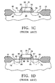
- FIGs. 1A-1D are cross-sectional views of a prior art sequence for forming an output MOSFET.
- FIG. 2 is a cross-sectional view of an output MOSFET formed by a prior art process of silicide blanking.
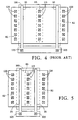
- FIG. 3 is a cross-sectional view of a first output buffer embodiment of the present invention, having extended sidewall oxide layers and lightly doped regions.
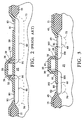
- FIG. 4 is a top view of a prior art output MOSFET of FIG. 2.
- FIG. 5 is a top view of an output buffer of the embodiment shown in FIG. 3.
- FIG. 6 is a second embodiment of an output buffer of the present invention, having an gate exposed for silicidation.
- FIG. 7 is a third embodiment of the present invention, showing the gate exposed for silicidation and having an oxide layer extending on only one side.
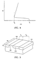
- FIG. 8 is a graph of voltage versus current for a MOSFET device undergoing bipolar snapback conduction.
- FIG. 9 is a cutaway perspective view of an ESD protection structure.
- FIG. 10 is a top view of an input/output transceiver of the present invention connected to a bond pad.
- a prior art formation of a MOSFET N-channel (NMOS) input or output transistor begins with the formation of rows of field oxide (FOX) 15 at a surface 20 of a substrate 25.
- the substrate 25 is typically a P-type silicon (Si) wafer for N-channel devices such as this example, and the FOX 15 is formed of silicon dioxide (SiO 2 ) which is grown into and onto the surface 20.
- the FOX 15 is formed of silicon dioxide (SiO 2 ) which is grown into and onto the surface 20.
- a dielectric layer of SiO 2 30 Disposed between the rows of FOX 15 is a dielectric layer of SiO 2 30 which has been grown and is covered by a polysilicon gate 35.
- the insulative layer 30 separating the gate 35 from the surface 20 is known as the gate oxide 30.
- FIG. 1B shows the formation of N-type lightly doped drain regions 40 within the substrate 25 between the polysilicon gate 35 and the FOX 15 rows.
- a blanket oxide layer 45 is subsequently formed which covers the FOX 15, surface 20, gate oxide 30 and gate 35.
- FIG. 1C shows the result of an anisotropic blanket etch of the prior art on the structure of FIG. 1B.
- Small sidewall oxide spacers 50 are left covering edges 55 and 56 of the polysilicon gate 35 and oxide layer 30. These spacers 50 remain after a controlled period of anisotropic etching due to the greater thickness of the oxide layer 45 at steps where the surface 20 and the edges 55 and 56 meet, while the etching exposes areas 80 and 81.
- FIG. 1D shows the result of implantation into the substrate 25 of self-aligned, heavily doped N+ regions to form a source 70 and a drain 75.
- Exposed areas 80 and 81 of the surface 20 are then heated and exposed to a refractory metal to anneal the implanted substrate 25 and to form silicide at the exposed areas 80 and 81.
- a silicide area 82 thus adjoins the source 70 and another silicide area 83 adjoins the drain 75.
- a top 85 of the gate 35 may also be coated with silicide or may be coated with an oxide layer, not shown. Conventional processes are then followed to connect the top 85 of the gate 30 and silicide areas 82 and 83 of the source 70 and drain 75 with external circuitry.
- the external circuitry may include a bond pad, not shown, which can provide an ESD event that destroys the dielectric gate oxide 30. Due to the conductivity of the gate 35, ESD damage occurs most frequently near corners 86 and 87 located at intersections of a bottom 88 of the gate 35 and, respectively, edges 55 and 56.
- the small spacers 50 of the prior art serve two purposes. The first is to spatially separate the source-drain regions which are exposed for silicidation 82 and 83 from the sidewalls of the gate electrode 55 and 56. Without these spacers, silicide would form over the sidewalls of the gate electrode 55 and 56 and provide a conductive path to the silicided regions 82 and 83, rendering the device inoperable.
- the incorporation of silicided source-drains is intended to increase the performance of advanced MOS technologies by minimizing the parasitic resistances of the source-drain regions.
- the second purpose of the sidewall spacers 50 is to provide a self-aligned mask for the formation of the heavily doped source-drain regions 70 and 75, thus allowing the formation of lightly doped drain regions 90 and 95.
- These lightly doped drain regions reduce the peak electric field at the drain of the device for a given applied voltage by terminating the drain potential less abruptly. This reduction in peak electric field reduces the generation of hot carriers in the channel, thus improving the short channel reliability and stability of the device.
- the silicide areas 82 and 83 have shunted passive resistance of heavily doped source and drain regions which previously provided some protection to the device from an ESD event, and the small LDD resistance in regions 90 and 95 has not been enough the make up for it.
- an ESD event can melt the metal in the silicided areas 82 and 83, which then flow along field lines caused by the event and directed between the source 70 and drain 75, increasing the conductance along those field lines. This unstable dispersion of power from an ESD event can lead to permanent metal filaments connecting the source 70 and drain 75 or holes burned through the substrate 25.
- FIG. 2 shows a structure similar to that of FIG. 1, but with the additional steps and additional material used in silicide blanking.
- An oxide layer 100 covers the FOX 15, gate 35, spacers 50 and surface 20 of the substrate 25 aside from the exposed areas 80 and 81 which are subsequently formed into silicide.
- the areas 80 and 81 are etched from the oxide layer 100 with conventional photolithography and etching so that silicide can be formed in those areas.
- the heavily doped drain 75 can be seen to extend much further along the surface 20 in order to add resistance for ESD protection between the silicide 83 over the drain 75 and the edge 56 of the gate 35.
- portions 90 and 95 of lightly doped regions 40 also add series resistance.
- Source silicide 82 is shown closer to the gate 35 than drain silicide 83, as less ESD protection may be needed adjacent source silicide 82.
- a first embodiment of an input or output transistor of the present invention is shown to include FOX rows 15 formed at a surface 20 of a silicon substrate 25, a gate oxide 30 and gate 35 are formed as described above under the prior art. Relatively extensive lightly doped drains 40 are formed between the gate oxide 30 and the FOX 15. A blanket dielectric oxide layer 45 is formed on top of the FOX 15, the surface 20, the gate oxide 30 and the gate 35, again as known in the prior art. The oxide layer is then masked and selectively etched to expose areas 80 and 81 of the surface 20 for silicide. The selective etching of the oxide 45 allows the formation of layers 102 and 103 which extend laterally further from the gate 35 and gate oxide 30 than the oxide spacers 50 of FIG. 1 created by the anisotropic etching of the prior art.
- the selective etching of the present invention is performed by first patterning a mask to cover areas of the oxide 45 that are desired to be left intact, such as the areas to form oxide layers 102 and 103 and to expose areas of the oxide 45 to be removed, such as those for silicided areas 80 and 81.
- a standard dry spacer oxide etch is then performed so that normal sidewall spaces are formed elsewhere on the circuit where ESD protection is not required, such as the die interior to the input/output devices. It should be noted that other electrically insulative materials could be used in place of the oxide layer 45 provided that selective etching of those materials is possible.
- Heavily doped regions formed preferably by ion implantation, are then created in the substrate 25 via the areas 80 and 81 exposed by selective etching. In this manner a source 70 and drain 75 are formed.
- the substrate is then annealed to correct possible damage to the crystalline substrate 25 caused by the ion implantation, and then silicide is formed at the exposed areas 80 and 81. As before, silicide area 82 adjoins the source 70 and silicide area 83 adjoins the drain 75.
- the length of the oxide layer 102 between the gate oxide 30 and the silicided area 82 can be seen to control the length of a portion 105 of the lightly doped region 40 that functions as a series resistor between the corner 86 and the silicide area 82 over the source 70.
- the length of the oxide layer 103 between the edge 56 and the silicide area 83 can be seen to control the length of a portion 110 of the lightly doped region 40 that functions as a series resistor between the corner 87 and the silicide area 83 over the drain.
- the total resistance provided by the portions 105 and 110 is adjustable by a masked dimension of the sidewall oxide 45.
- the symmetrical lightly doped regions 105 and 110 of this embodiment may be preferred for bidirectional transistors and may have a channel length of 0.3 microns to 6 microns. As will be discussed below, the exact length of the lightly doped regions 105 and 110 can be tailored to provide an optimized ESD protection structure.
- lightly doped regions 105 and 110 acts to prevent ESD damage also by dispersing the path of an ESD current. Without these lightly doped regions 105 and 110, the shortest electrical path between any combination of the source 70, the gate 35 and the drain 75 is along the surface 20.
- the highly conductive silicided surface areas 82 and 83 also tend to concentrate current along the surface 20. A greater concentration of current during an ESD event will tend to increase the damage caused by that event. Lightly doped regions 105 and 110 tend to disperse the current away from the surface 20, increasing the tolerance to ESD.
- the substrate 25 could be N-type silicon
- the source 70 and drain 75 could be doped P+ and the lightly doped drains 40 doped with similarly charged ions to instead form a P-channel transistor (PMOS).
- PMOS P-channel transistor
- CMOS complementary of N-channel and P-channel device
- a conventional CMOS process flow is then followed.
- the lightly doped implants 40 and heavily doped regions 70 and 75 can be doped earlier in the formative steps outlined above, instead of or in addition to the self-aligned doping described above.
- the lightly doped regions 105 and 110 of the present invention can extend further than the portions 90 and 95 of the prior art, as the sidewall oxide layers 102 and 103 of the present invention can extend further than the spacers 50 of the prior art. Due to the anisotropic etching employed in the prior art, the maximum lateral extent of the spacers 50 of the prior art was effectively limited to the lesser of a thickness of oxide layer 45 or a height of the top 85 of the gate 35 from the surface 20. The appreciable extent of lightly doped region 105 forms a larger series resistance between the source 70 and the gate 35 than provided by portion 90. Similarly, the significant extent of lightly doped region 110 forms a larger series resistance between the gate 35 and the drain 75 than that of portion 95, providing improved protection against ESD.
- the lightly doped region 110 may, despite its smaller size than region 40 of FIG. 2, provide more resistance than the larger distance between the corner 87 and silicide surface 80 over the drain 75 provided by silicon blanking. This is due to the higher unit resistance of the lightly doped region 110 than that of the heavily doped drain 75 of the silicide blanked structure.
- the silicide blanked structure can require more vertical space and material, as well as extra horizontal space and material, compared with the present invention.
- the silicide blanking also adds at least one extra processing step over that required for the present invention, due to the formation of blanking oxide 100.
- the silicon blanking shown in FIG. 2 although providing increased ESD protection over that provided by spacer oxides 50 of FIG. 1, may provide less ESD protection and require more space and material than the present invention.
- FIG. 4 the large separation between a drain contact 115 and a gate 35 for the prior art devices formed by the silicide blanking oxide layer 100 of FIG. 2 can be seen in this view of a top of an output transistor.
- the large separation required by this technology is due to the relatively high conductivity of the drain region 40 underlying most of the space between the gate 35 and the drain silicide 83.
- Source contacts 120, gate contacts 125 and source silicided region 82 are shown for reference.
- FIG. 5 a portion of a top of an output transistor made by the present technology can be seen in FIG. 5 to have a much smaller separation between drain contacts 115 and gate 35. As such, smaller input/output transistors can be used on an IC while achieving a higher ESD immunity using the present invention.
- FIG. 6 shows a second embodiment of the present invention, in which the top 85 of the gate has also been exposed by selective etching. This allows silicidation of the top 85, for subsequent metallization and interconnection with other circuitry, not shown.
- the numbers shown in FIG. 6 refer to the same parts as corresponding numbers in previous FIGs. In general, the structure shown in FIG. 6 is used where it is desirable for the gate 35 to have a low resistance due to the silicide formation on it.
- the controllable length of oxide layers 102 and 103 can be used to tailor the extension of lightly doped regions 105 and 110, in concert with the doping concentration of regions 105 and 110, for optimal device performance and ESD immunity.
- the length of lightly doped region 110 may be desired to be larger than that of lightly doped region 105. This may also be advantageous in avoiding hot carrier effects, which can destroy a gate oxide in a manner similar to but less dramatically than an ESD event.
- FIG. 7 depicts another embodiment of the present invention, in which the selective etching of the oxide layer 45 has left a sidewall oxide layer 103 between the edge 56 of the polysilicon gate 35 and the drain 75, which results in a lightly doped drain region 110 between the gate 35 and the drain 75 of significant extent.
- Most of the top 85 of the gate 35 has been exposed by etching, to enable subsequent silicide formation on the gate 35.
- a standard sidewall oxide spacer 102 has been left between the edge 55 of the gate oxide 30 and the source 70 to prevent silicide formation from source to gate. This has been accomplished in this embodiment by exposing a portion of the source 70 and the gate 35 to the spacer etch with conventional photo masking.
- This oxide spacer 102 minimizes the resistance between the source 70 and the gate 35 provided by lightly doped source region 105 for improved circuit performance in those circuits which do not require ESD protection between the source 70 and the gate 35.
- the optimal extent of the sidewall oxide layers 102 and 103, and the resultant series resistance provided by lightly doped source and drain regions 102 and 103 involves a tradeoff between ESD protection and performance needs, as greater ESD protection typically entails more extensive series resistance, while improved circuit performance typically requires less series resistance.
- the present invention also allows a means of optimizing the performance and ESD mitigation of a circuit by tailoring the length of the selectively etched sidewall layers to achieve an optimal series resistance. For example, for a typical transistor used as an output buffer, ESD protection near the drain is more essential, and the sidewall oxide layer 103 can be more extensive than layer 102 in order to increase the resistance provided by lightly doped drain region 110, as shown in FIGs. 5 and 6.
- a bidirectional transistor may benefit from equal ESD protection in series between the gate and both the source and drain, as shown by the substantially equal extent of lightly doped regions 105 and 110 shown in FIGs. 3 and 6.
- Input/output transistors commonly have channel lengths, which are measured as the distance between the source and drain, that are much smaller than channel widths, which are measured in the direction that polysilicon gates 35 of FIG. 5 extend, for example.
- the reason for this small length to width aspect ratio is to allow fast, high-powered transistor action for communication with circuits external to the IC chip or for overcoming loads encountered internally on the chip.
- This large channel width which may be several hundred microns (compared to a channel length of about one micron) may be used to absorb an ESD pulse through bipolar snapback conduction across the channel.
- a current (I) versus voltage (V) graph for a transistor in snapback conduction shows that no current flows through the device between source and drain until the voltage has reached the trigger voltage (V t ).
- the present invention adds a series resistance due to a lightly doped region such as region 110 of FIG. 3.
- This series, resistance is selected to be sufficient to add a voltage due to the flow of current through the path in which snapback has been initiated that raises the voltage of that path above the trigger voltage (V t ), causing adjacent paths to be at or above V t and to also begin snapback conduction.
- This spreading of snapback conduction across the width and depth of the channel defocuses the snapback current from a single, concentrated path to a wide swath that may extend the width and depth of the channel.
- the spreading of current must occur before the current in a path has exceeded a maximum nondestructive current density (I m ), which can be empirically determined by testing similar devices.
- I m nondestructive current density
- the ESD current can be estimated using known ESD parameters, such as a Human Body Model voltage of 2500 V, and an intrinsic resistance between a person and a bond pad of perhaps 1500 ⁇ .
- Other ESD failsafe criteria such as the Machine Model or other parameters selected for a particular application, may instead be employed.
- FIG. 9 a perspective diagram of doped sections of a semiconductor substrate that form an ESD protection structure of the current invention are shown to include a source 120 and drain 122 which are heavily doped and a lightly doped drain extension 124, with an opposite conductivity type channel 126 disposed between the extension 124 and the source 120.
- the channel 126 has a length (L c ) separating the source 120 and the extension 124, a width (W) and depth (D) oriented transversely to that length (L c ).
- the drain extension 124 has a similar length and width as the channel 126, the extension having an extent (E d ) measured between the drain 122 and channel 126.
- the series resistance (R s ) of a localized path conducting current at I m must be sufficient to cause the voltage of that path to equal or exceed V t .
- the series resistance (R s ) is the sum of the resistance in the channel during snapback conduction (as shown graphically by the upward sloping portion of the curve in FIG. 8) and the resistance of the lightly doped extension of the drain.
- the resistance in the channel is equal to the channel resistivity during snapback ( ⁇ c ) multiplied by the channel length (L c ) and divided by the channel area (A c ).
- the channel area (A c ) is equal to the channel width (W) times depth (D) and is essentially equal in magnitude to an area (A d ) of the extension 124, so that both areas may be termed simply A.
- the resistance in the lightly doped extension of the drain is equal to the resistivity ( ⁇ d ) of that lightly doped region, which can be determined by doping concentrations and doses, multiplied by the lightly doped extent (E d ) divided by the extension area (A) orthogonal to the extent (E d ). Current limiting each path to less than I m yields: V t - V H R s ⁇ I m A
- an ESD current (I esd ) which may be 2500 V/1500 ⁇ or a different selected amperage, multiplied by R s must be less than or equal to V g - V H : I esd R s ⁇ V g - V H or A ⁇ I esd ( ⁇ c L c + ⁇ d E d ) V g - V H
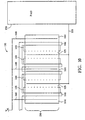
- a top view of an input/output transceiver 130 shows a metal connection 133 between drain regions 135 of the transceiver 130 and an input/output terminal or bond pad 138.
- Metal connections 140 between source regions 144 and V ss provide a path for an ESD pulse that has traversed the transceiver 130 without damage according to the present invention to be absorbed in a power supply or ground.
- the dashed rectangles indicate borders of lightly doped drain extensions 148 which terminate near an edge of a polysilicon gate 146. Beneath the gate 146 and between the extensions 148 and the source regions 144 are channels, not shown. Note that the channel width (W) in this interspaced transceiver is four times the width 150 of each individual channel.
- I max the maximum nondestructive snapback current per micron of channel width (W) and R SH as the sheet resistance of the lightly doped region 124
- the doping of the lightly doped drain regions may be adjusted during device formation to produce a concentration of between 1 x 10 17 and 5 x 10 19 ions/cm 3 , or a sheet resistance of 100-5,000 Ohms/square.
- the width (W) of the channel may be in a range between less than 100 to greater than 300 microns, while the length (L c ) of the channel may be on the order of one micron to induce snapback conduction.
- the extent (E d ) of the lightly doped drain extension may be between 0.3 micron and 6.0 microns, and preferably around 0.5 micron to 2.0 microns and at least as large as the channel length (L c ).
Landscapes
- Insulated Gate Type Field-Effect Transistor (AREA)
- Semiconductor Integrated Circuits (AREA)
- Metal-Oxide And Bipolar Metal-Oxide Semiconductor Integrated Circuits (AREA)
Applications Claiming Priority (3)
| Application Number | Priority Date | Filing Date | Title |
|---|---|---|---|
| US18071694A | 1994-01-12 | 1994-01-12 | |
| US180716 | 1994-01-12 | ||
| PCT/US1995/000580 WO1995019646A1 (en) | 1994-01-12 | 1995-01-12 | Input/output transistors with optimized esd protection |
Publications (3)
| Publication Number | Publication Date |
|---|---|
| EP0739542A1 EP0739542A1 (en) | 1996-10-30 |
| EP0739542A4 EP0739542A4 (en) | 1997-04-16 |
| EP0739542B1 true EP0739542B1 (en) | 2002-05-02 |
Family
ID=22661485
Family Applications (1)
| Application Number | Title | Priority Date | Filing Date |
|---|---|---|---|
| EP95910093A Expired - Lifetime EP0739542B1 (en) | 1994-01-12 | 1995-01-12 | Input/output transistors with optimized esd protection |
Country Status (8)
| Country | Link |
|---|---|
| US (1) | US5493142A (enExample) |
| EP (1) | EP0739542B1 (enExample) |
| JP (1) | JPH09507723A (enExample) |
| KR (1) | KR100320354B1 (enExample) |
| CN (1) | CN1047027C (enExample) |
| DE (1) | DE69526569T2 (enExample) |
| TW (1) | TW262584B (enExample) |
| WO (1) | WO1995019646A1 (enExample) |
Cited By (1)
| Publication number | Priority date | Publication date | Assignee | Title |
|---|---|---|---|---|
| US9177924B2 (en) | 2013-12-18 | 2015-11-03 | Taiwan Semiconductor Manufacturing Company Limited | Vertical nanowire transistor for input/output structure |
Families Citing this family (42)
| Publication number | Priority date | Publication date | Assignee | Title |
|---|---|---|---|---|
| US5374565A (en) * | 1993-10-22 | 1994-12-20 | United Microelectronics Corporation | Method for ESD protection improvement |
| US5675168A (en) * | 1994-04-01 | 1997-10-07 | Matsushita Electric Industrial Co., Ltd. | Unsymmetrical MOS device having a gate insulator area offset from the source and drain areas, and ESD protection circuit including such a MOS device |
| JPH0951078A (ja) * | 1995-05-29 | 1997-02-18 | Mitsubishi Electric Corp | 半導体記憶装置および半導体装置 |
| KR100402672B1 (ko) * | 1995-10-31 | 2004-06-04 | 텍사스 인스트루먼츠 인코포레이티드 | CMOS/BiCMOS기술에서ESD방지를위한집적화된횡형구조 |
| US5869869A (en) * | 1996-01-31 | 1999-02-09 | Lsi Logic Corporation | Microelectronic device with thin film electrostatic discharge protection structure |
| US6071768A (en) * | 1996-05-17 | 2000-06-06 | Texas Instruments Incorporated | Method of making an efficient NPN turn-on in a high voltage DENMOS transistor for ESD protection |
| JPH1070266A (ja) * | 1996-08-26 | 1998-03-10 | Nec Corp | 半導体装置およびその製造方法 |
| US5953601A (en) * | 1998-02-17 | 1999-09-14 | Taiwan Semiconductor Manufacturing Company, Ltd. | ESD implantation scheme for 0.35 μm 3.3V 70A gate oxide process |
| US6171891B1 (en) | 1998-02-27 | 2001-01-09 | Taiwan Semiconductor Manufacturing Company | Method of manufacture of CMOS device using additional implant regions to enhance ESD performance |
| FR2779574B1 (fr) * | 1998-06-03 | 2003-01-31 | Sgs Thomson Microelectronics | Procede de fabrication de transistors haute et basse tension |
| TW399337B (en) * | 1998-06-09 | 2000-07-21 | Koninkl Philips Electronics Nv | Semiconductor device |
| US6100125A (en) * | 1998-09-25 | 2000-08-08 | Fairchild Semiconductor Corp. | LDD structure for ESD protection and method of fabrication |
| JP4589468B2 (ja) * | 1998-11-06 | 2010-12-01 | セイコーエプソン株式会社 | Mosトランジスタの製造方法およびmosトランジスタ |
| US6268639B1 (en) | 1999-02-11 | 2001-07-31 | Xilinx, Inc. | Electrostatic-discharge protection circuit |
| TW409392B (en) * | 1999-05-10 | 2000-10-21 | United Microelectronics Corp | Fabrication method of improving the electrostatic discharge ability of the device and increasing the gain of connected bipolar transistor |
| US6285062B1 (en) * | 1999-05-12 | 2001-09-04 | Micron Technology, Inc. | Adjustable high-trigger-voltage electrostatic discharge protection device |
| US6646324B1 (en) * | 2000-06-30 | 2003-11-11 | Intel Corporation | Method and apparatus for a linearized output driver and terminator |
| US6444404B1 (en) | 2000-08-09 | 2002-09-03 | Taiwan Semiconductor Manufacturing Company | Method of fabricating ESD protection device by using the same photolithographic mask for both the ESD implantation and the silicide blocking regions |
| US6704180B2 (en) | 2002-04-25 | 2004-03-09 | Medtronic, Inc. | Low input capacitance electrostatic discharge protection circuit utilizing feedback |
| US8089129B2 (en) * | 2002-08-14 | 2012-01-03 | Advanced Analogic Technologies, Inc. | Isolated CMOS transistors |
| US7825488B2 (en) | 2006-05-31 | 2010-11-02 | Advanced Analogic Technologies, Inc. | Isolation structures for integrated circuits and modular methods of forming the same |
| JP2004111746A (ja) * | 2002-09-19 | 2004-04-08 | Fujitsu Ltd | 半導体装置及びその製造方法 |
| JP3808026B2 (ja) * | 2002-10-23 | 2006-08-09 | 株式会社ルネサステクノロジ | 半導体装置 |
| JP2005109389A (ja) * | 2003-10-02 | 2005-04-21 | Sanyo Electric Co Ltd | 半導体装置及びその製造方法 |
| US7508038B1 (en) | 2005-04-29 | 2009-03-24 | Zilog, Inc. | ESD protection transistor |
| US7646063B1 (en) | 2005-06-15 | 2010-01-12 | Pmc-Sierra, Inc. | Compact CMOS ESD layout techniques with either fully segmented salicide ballasting (FSSB) in the source and/or drain regions |
| JP4711061B2 (ja) | 2005-09-13 | 2011-06-29 | セイコーエプソン株式会社 | 半導体装置 |
| US7385263B2 (en) * | 2006-05-02 | 2008-06-10 | Atmel Corporation | Low resistance integrated MOS structure |
| TWI339886B (en) * | 2006-09-14 | 2011-04-01 | Novatek Microelectronics Corp | Layout structure of electrostatic discharge protection circuit and production method thereof |
| JP5217180B2 (ja) | 2007-02-20 | 2013-06-19 | 富士通セミコンダクター株式会社 | 静電放電保護装置の製造方法 |
| JP2007194656A (ja) * | 2007-03-16 | 2007-08-02 | Seiko Epson Corp | Mosトランジスタの製造方法およびmosトランジスタ |
| KR100976793B1 (ko) * | 2007-12-31 | 2010-08-20 | 주식회사 동부하이텍 | 모스 트랜지스터의 제조 방법 |
| US8354710B2 (en) | 2008-08-08 | 2013-01-15 | Infineon Technologies Ag | Field-effect device and manufacturing method thereof |
| KR101051684B1 (ko) * | 2008-12-02 | 2011-07-25 | 매그나칩 반도체 유한회사 | 정전기 방전 보호소자 및 그 제조방법 |
| JP5202473B2 (ja) | 2009-08-18 | 2013-06-05 | シャープ株式会社 | 半導体装置の製造方法 |
| CN101807605B (zh) * | 2010-02-05 | 2015-05-06 | 上海华虹宏力半导体制造有限公司 | 一种半导体器件及其制造方法 |
| GB2540904B (en) * | 2010-10-08 | 2017-05-24 | Dnae Group Holdings Ltd | Electrostatic discharge protection |
| US8536648B2 (en) | 2011-02-03 | 2013-09-17 | Infineon Technologies Ag | Drain extended field effect transistors and methods of formation thereof |
| JP5705593B2 (ja) * | 2011-03-08 | 2015-04-22 | セイコーインスツル株式会社 | 半導体装置および半導体装置の製造方法 |
| US8643111B1 (en) * | 2012-08-22 | 2014-02-04 | Vanguard International Semiconductor Corporation | Electrostatic discharge (ESD) protection device |
| KR102832118B1 (ko) * | 2020-03-04 | 2025-07-08 | 주식회사 디비하이텍 | Esd 보호소자 및 제조방법 |
| US20240154406A1 (en) * | 2022-11-08 | 2024-05-09 | Qualcomm Incorporated | Symmetric radio frequency (rf) electrostatic discharge (esd) dissipation switch |
Citations (1)
| Publication number | Priority date | Publication date | Assignee | Title |
|---|---|---|---|---|
| US5248892A (en) * | 1989-03-13 | 1993-09-28 | U.S. Philips Corporation | Semiconductor device provided with a protection circuit |
Family Cites Families (9)
| Publication number | Priority date | Publication date | Assignee | Title |
|---|---|---|---|---|
| US5276346A (en) * | 1983-12-26 | 1994-01-04 | Hitachi, Ltd. | Semiconductor integrated circuit device having protective/output elements and internal circuits |
| US4692781B2 (en) * | 1984-06-06 | 1998-01-20 | Texas Instruments Inc | Semiconductor device with electrostatic discharge protection |
| JPS62274767A (ja) * | 1986-05-23 | 1987-11-28 | Fujitsu Ltd | 高耐圧半導体装置及びその製造方法 |
| US4855620A (en) * | 1987-11-18 | 1989-08-08 | Texas Instruments Incorporated | Output buffer with improved ESD protection |
| JP2698645B2 (ja) * | 1988-05-25 | 1998-01-19 | 株式会社東芝 | Mosfet |
| US5283449A (en) * | 1990-08-09 | 1994-02-01 | Nec Corporation | Semiconductor integrated circuit device including two types of MOSFETS having source/drain region different in sheet resistance from each other |
| US5208475A (en) * | 1991-01-30 | 1993-05-04 | National Semiconductor Corporation | Electrostatic discharge protection device and a method for simultaneously forming MOS devices with both lightly doped and non lightly doped source and drain regions |
| KR930010124B1 (ko) * | 1991-02-27 | 1993-10-14 | 삼성전자 주식회사 | 반도체 트랜지스터의 제조방법 및 그 구조 |
| US5146298A (en) * | 1991-08-16 | 1992-09-08 | Eklund Klas H | Device which functions as a lateral double-diffused insulated gate field effect transistor or as a bipolar transistor |
-
1995
- 1995-01-12 DE DE69526569T patent/DE69526569T2/de not_active Expired - Fee Related
- 1995-01-12 EP EP95910093A patent/EP0739542B1/en not_active Expired - Lifetime
- 1995-01-12 WO PCT/US1995/000580 patent/WO1995019646A1/en not_active Ceased
- 1995-01-12 KR KR1019960701888A patent/KR100320354B1/ko not_active Expired - Fee Related
- 1995-01-12 JP JP7519171A patent/JPH09507723A/ja not_active Ceased
- 1995-01-12 CN CN95190969A patent/CN1047027C/zh not_active Expired - Fee Related
- 1995-02-22 TW TW084101628A patent/TW262584B/zh not_active IP Right Cessation
- 1995-03-02 US US08/397,584 patent/US5493142A/en not_active Expired - Lifetime
Patent Citations (1)
| Publication number | Priority date | Publication date | Assignee | Title |
|---|---|---|---|---|
| US5248892A (en) * | 1989-03-13 | 1993-09-28 | U.S. Philips Corporation | Semiconductor device provided with a protection circuit |
Cited By (3)
| Publication number | Priority date | Publication date | Assignee | Title |
|---|---|---|---|---|
| US9177924B2 (en) | 2013-12-18 | 2015-11-03 | Taiwan Semiconductor Manufacturing Company Limited | Vertical nanowire transistor for input/output structure |
| US10510744B2 (en) | 2013-12-18 | 2019-12-17 | Taiwan Semiconductor Manufacturing Company, Ltd. | Vertical nanowire transistor for input/output structure |
| US11127734B2 (en) | 2013-12-18 | 2021-09-21 | Taiwan Semiconductor Manufacturing Company Limited | Vertical nanowire transistor for input/output structure |
Also Published As
| Publication number | Publication date |
|---|---|
| CN1047027C (zh) | 1999-12-01 |
| CN1136367A (zh) | 1996-11-20 |
| EP0739542A1 (en) | 1996-10-30 |
| DE69526569T2 (de) | 2002-12-19 |
| EP0739542A4 (en) | 1997-04-16 |
| US5493142A (en) | 1996-02-20 |
| TW262584B (enExample) | 1995-11-11 |
| DE69526569D1 (de) | 2002-06-06 |
| KR100320354B1 (ko) | 2002-06-24 |
| JPH09507723A (ja) | 1997-08-05 |
| KR960705364A (ko) | 1996-10-09 |
| WO1995019646A1 (en) | 1995-07-20 |
Similar Documents
| Publication | Publication Date | Title |
|---|---|---|
| EP0739542B1 (en) | Input/output transistors with optimized esd protection | |
| US6873017B2 (en) | ESD protection for semiconductor products | |
| EP0982776B1 (en) | ESD protection thyristor with trigger diode | |
| US5468667A (en) | Method of placing source contacts for efficient ESD/EOS protection in grounded substrate MOS integrated circuit | |
| JPH09213811A (ja) | 電子回路を静電放電による破壊から保護するための装置、方法およびシステム | |
| JPH10504424A (ja) | 静電放電保護回路 | |
| JPH0433139B2 (enExample) | ||
| US6835624B2 (en) | Semiconductor device for protecting electrostatic discharge and method of fabricating the same | |
| JP4620282B2 (ja) | 半導体装置 | |
| US6215156B1 (en) | Electrostatic discharge protection device with resistive drain structure | |
| EP1132971B1 (en) | Electrostatic discharge protection transistor | |
| US8093121B1 (en) | ESD protection transistor | |
| JP3317345B2 (ja) | 半導体装置 | |
| JP2000243850A (ja) | 半導体デバイスの形成方法 | |
| US6040603A (en) | Electrostatic discharge protection circuit employing MOSFETs having double ESD implantations | |
| EP0772238A2 (en) | Semiconductor device with protecting means | |
| JP2755619B2 (ja) | 絶縁ゲート型半導体装置 | |
| JP3036448B2 (ja) | 半導体装置 | |
| US20020145165A1 (en) | Semiconductor device having electrostatic discharge protector and fabricating method thereof | |
| JP2001168321A (ja) | 半導体保護装置とその保護方法 | |
| JP2830630B2 (ja) | 半導体装置およびその製造方法 | |
| JP3390336B2 (ja) | 半導体集積回路装置及びその製造方法 | |
| JP3187773B2 (ja) | 入力保護素子を備えた半導体装置 | |
| JPH0563191A (ja) | 半導体装置 | |
| JPH09199609A (ja) | Mos集積回路およびその製造方法 |
Legal Events
| Date | Code | Title | Description |
|---|---|---|---|
| PUAI | Public reference made under article 153(3) epc to a published international application that has entered the european phase |
Free format text: ORIGINAL CODE: 0009012 |
|
| 17P | Request for examination filed |
Effective date: 19960812 |
|
| AK | Designated contracting states |
Kind code of ref document: A1 Designated state(s): DE FR GB IT NL |
|
| A4 | Supplementary search report drawn up and despatched |
Effective date: 19970227 |
|
| AK | Designated contracting states |
Kind code of ref document: A4 Designated state(s): DE FR GB IT NL |
|
| 17Q | First examination report despatched |
Effective date: 19990614 |
|
| GRAG | Despatch of communication of intention to grant |
Free format text: ORIGINAL CODE: EPIDOS AGRA |
|
| GRAG | Despatch of communication of intention to grant |
Free format text: ORIGINAL CODE: EPIDOS AGRA |
|
| GRAH | Despatch of communication of intention to grant a patent |
Free format text: ORIGINAL CODE: EPIDOS IGRA |
|
| GRAH | Despatch of communication of intention to grant a patent |
Free format text: ORIGINAL CODE: EPIDOS IGRA |
|
| REG | Reference to a national code |
Ref country code: GB Ref legal event code: IF02 |
|
| GRAA | (expected) grant |
Free format text: ORIGINAL CODE: 0009210 |
|
| AK | Designated contracting states |
Kind code of ref document: B1 Designated state(s): DE FR GB IT NL |
|
| REG | Reference to a national code |
Ref country code: GB Ref legal event code: FG4D |
|
| REF | Corresponds to: |
Ref document number: 69526569 Country of ref document: DE Date of ref document: 20020606 |
|
| ET | Fr: translation filed | ||
| PLBE | No opposition filed within time limit |
Free format text: ORIGINAL CODE: 0009261 |
|
| STAA | Information on the status of an ep patent application or granted ep patent |
Free format text: STATUS: NO OPPOSITION FILED WITHIN TIME LIMIT |
|
| 26N | No opposition filed |
Effective date: 20030204 |
|
| PGFP | Annual fee paid to national office [announced via postgrant information from national office to epo] |
Ref country code: GB Payment date: 20041231 Year of fee payment: 11 |
|
| PGFP | Annual fee paid to national office [announced via postgrant information from national office to epo] |
Ref country code: FR Payment date: 20050118 Year of fee payment: 11 |
|
| PGFP | Annual fee paid to national office [announced via postgrant information from national office to epo] |
Ref country code: NL Payment date: 20050131 Year of fee payment: 11 Ref country code: DE Payment date: 20050131 Year of fee payment: 11 |
|
| PG25 | Lapsed in a contracting state [announced via postgrant information from national office to epo] |
Ref country code: GB Free format text: LAPSE BECAUSE OF NON-PAYMENT OF DUE FEES Effective date: 20060112 |
|
| PG25 | Lapsed in a contracting state [announced via postgrant information from national office to epo] |
Ref country code: FR Free format text: LAPSE BECAUSE OF NON-PAYMENT OF DUE FEES Effective date: 20060131 |
|
| PGFP | Annual fee paid to national office [announced via postgrant information from national office to epo] |
Ref country code: IT Payment date: 20060131 Year of fee payment: 12 |
|
| PG25 | Lapsed in a contracting state [announced via postgrant information from national office to epo] |
Ref country code: NL Free format text: LAPSE BECAUSE OF NON-PAYMENT OF DUE FEES Effective date: 20060801 Ref country code: DE Free format text: LAPSE BECAUSE OF NON-PAYMENT OF DUE FEES Effective date: 20060801 |
|
| GBPC | Gb: european patent ceased through non-payment of renewal fee |
Effective date: 20060112 |
|
| NLV4 | Nl: lapsed or anulled due to non-payment of the annual fee |
Effective date: 20060801 |
|
| REG | Reference to a national code |
Ref country code: FR Ref legal event code: ST Effective date: 20060929 |
|
| PG25 | Lapsed in a contracting state [announced via postgrant information from national office to epo] |
Ref country code: IT Free format text: LAPSE BECAUSE OF NON-PAYMENT OF DUE FEES Effective date: 20070112 |