EP0713222B1 - Integrierte Speicherschaltungsanordnung - Google Patents
Integrierte Speicherschaltungsanordnung Download PDFInfo
- Publication number
- EP0713222B1 EP0713222B1 EP95307998A EP95307998A EP0713222B1 EP 0713222 B1 EP0713222 B1 EP 0713222B1 EP 95307998 A EP95307998 A EP 95307998A EP 95307998 A EP95307998 A EP 95307998A EP 0713222 B1 EP0713222 B1 EP 0713222B1
- Authority
- EP
- European Patent Office
- Prior art keywords
- circuitry
- signal
- line
- memory device
- integrated circuit
- Prior art date
- Legal status (The legal status is an assumption and is not a legal conclusion. Google has not performed a legal analysis and makes no representation as to the accuracy of the status listed.)
- Expired - Lifetime
Links
- 230000015654 memory Effects 0.000 claims description 47
- 238000002955 isolation Methods 0.000 claims description 20
- 230000003213 activating effect Effects 0.000 claims 1
- 238000011067 equilibration Methods 0.000 description 44
- 101710170230 Antimicrobial peptide 1 Proteins 0.000 description 33
- 101710170231 Antimicrobial peptide 2 Proteins 0.000 description 33
- 238000003491 array Methods 0.000 description 9
- 238000010586 diagram Methods 0.000 description 6
- PWPJGUXAGUPAHP-UHFFFAOYSA-N lufenuron Chemical compound C1=C(Cl)C(OC(F)(F)C(C(F)(F)F)F)=CC(Cl)=C1NC(=O)NC(=O)C1=C(F)C=CC=C1F PWPJGUXAGUPAHP-UHFFFAOYSA-N 0.000 description 6
- 230000003321 amplification Effects 0.000 description 5
- 238000003199 nucleic acid amplification method Methods 0.000 description 5
- 230000001172 regenerating effect Effects 0.000 description 5
- 230000000295 complement effect Effects 0.000 description 4
- 230000004044 response Effects 0.000 description 4
- 230000009471 action Effects 0.000 description 3
- 238000000034 method Methods 0.000 description 3
- 230000003068 static effect Effects 0.000 description 3
- 230000008859 change Effects 0.000 description 2
- 230000008878 coupling Effects 0.000 description 2
- 238000010168 coupling process Methods 0.000 description 2
- 238000005859 coupling reaction Methods 0.000 description 2
- 230000001419 dependent effect Effects 0.000 description 2
- 230000010354 integration Effects 0.000 description 2
- 230000008569 process Effects 0.000 description 2
- 238000009825 accumulation Methods 0.000 description 1
- 230000004913 activation Effects 0.000 description 1
- 230000002457 bidirectional effect Effects 0.000 description 1
- 239000003990 capacitor Substances 0.000 description 1
- 238000009795 derivation Methods 0.000 description 1
- 230000000694 effects Effects 0.000 description 1
- 230000005684 electric field Effects 0.000 description 1
- 230000006870 function Effects 0.000 description 1
- 230000009467 reduction Effects 0.000 description 1
- 239000007787 solid Substances 0.000 description 1
- 239000000758 substrate Substances 0.000 description 1
Images


Classifications
-
- G—PHYSICS
- G11—INFORMATION STORAGE
- G11C—STATIC STORES
- G11C7/00—Arrangements for writing information into, or reading information out from, a digital store
- G11C7/06—Sense amplifiers; Associated circuits, e.g. timing or triggering circuits
- G11C7/065—Differential amplifiers of latching type
-
- G—PHYSICS
- G11—INFORMATION STORAGE
- G11C—STATIC STORES
- G11C16/00—Erasable programmable read-only memories
- G11C16/02—Erasable programmable read-only memories electrically programmable
- G11C16/06—Auxiliary circuits, e.g. for writing into memory
- G11C16/26—Sensing or reading circuits; Data output circuits
-
- G—PHYSICS
- G11—INFORMATION STORAGE
- G11C—STATIC STORES
- G11C7/00—Arrangements for writing information into, or reading information out from, a digital store
- G11C7/10—Input/output [I/O] data interface arrangements, e.g. I/O data control circuits, I/O data buffers
- G11C7/1048—Data bus control circuits, e.g. precharging, presetting, equalising
Definitions
- This invention relates to an integrated circuit memory device, and in particular to improved sensing circuits in an integrated circuit memory device.
- the invention is concerned with a memory device in which memory cells are formed by insulated gate transistors. These memories include EPROMs and FLASH EPROMs referred to herein as flash memories.
- EPROMs EPROMs
- FLASH EPROMs FLASH EPROMs referred to herein as flash memories.
- An EPROM cell is shown by publication "1990 IEEE International Solid State Circuits Conference: Digest of Technical papers, 14 February 1990 pages 58-60 (XP000201829): Atsumi et. al: Nonvolatile and Fast Static Memories". This document discloses the features of the preamble of claim 1.
- the sense amplifiers are implemented as static sense amplifiers.
- a static sense amplifier continuously senses the signal differential between its inputs.
- the inputs can be connected to the bit line of an accessed memory cell and a reference signal.
- the signal differential may be a current or a voltage differential. This signal differential is usually very small, and the sense amplifier must have a high gain and therefore requires more than one amplification stage.
- EP-A-0329910 shows a double stage sense amplifier for SRAMs comprising a latch. More particularly, EP-A-0329910 discloses a double stage sense amplifier comprised of a first stage and a second stage. The subsequent stages operate sequentially to amplify the data continuously along a sensing chain of the data path during a READ operation to provide a data output signal on data output nodes. The subsequent amplifiers include each a clocked latch circuitry.
- the double stage sense circuitry is connected between a data line pair and the SRAMs of the EP-A-0329910 are correspondingly connected between two bit lines and sensed by a sense amplifier circuitry that is connected between two data lines. Therefore a substantially different switching circuitry is required from that what is used in the above referenced disclosure by Atsumi et. al. discussing use of EPROMs.
- Each amplification stage requires accurate biasing in order to maintain the sensing stages in the regions of high gain in the presence of process skews.
- This requirement for accurate biasing necessitates the provision of accurate reference voltages for each amplification stage which is difficult to achieve, particularly for memory devices which are compatible with different power supply voltages.
- a typical memory chip can operate with a power supply voltage of 3.3V ⁇ 0.3V or with a power supply voltage of 5V ⁇ 10%.
- the actual power supply voltage therefore has extremes of 3.0V and 5.5V.
- the requirement for several amplification stages results in the sense amplifier circuitry occupying a large amount of chip area, and also having a high power requirement.
- EP-A-604 195 describes a dynamic sense amplifier.
- DRAM Dynamic RAM
- CMOS complementary metal-oxide-semiconductor
- Such a sense amplifier does not require accurate biasing and is therefore ideal for applications in which the supply voltage may vary over a wide range.
- Dynamic RAM (DRAM) cells comprise a storage element, consisting of a capacitor, and an access transistor.
- the regenerative feedback action of a dynamic sense amplifier RAM can be used to restore the level of the storage element in the cell, which is degraded during the read process, by writing the signal back onto the bit lines.
- the bit lines need to be maintained at a fairly low voltage (at less than 1V) in order to reduce stress, which would cause the stored data in the cells to be affected over a long period.
- an integrated circuit memory device as defined in claim 1.
- Figure 1 illustrates a flash memory cell 2 comprising a single floating gate transistor 4 having a control gate CG , a floating gate FG , a source S , and a drain D .
- the source S of the floating gate transistor 4 is connected to an ARRAY GROUND signal on line 10.
- this line 10 can be at a ground voltage VGND or a high voltage Vpp .
- Voltage Vpp represents a programming potential (typically 12V) and voltage VGND represents device ground.
- Vpp is normally connected to array ground, either directly or via a resistor (not shown).
- the source voltage switch 14 is connected to the voltage Vpp via line 34 and the voltage VGND via line 36.
- the control gate CG of the floating gate transistor 4 is connected to the output signal Vccx of a gate voltage switch 12 by a word line ( WL ) 8.
- the gate voltage switch 12 is further connected to voltages Vcc, Vpp and VGND on lines 26, 24 and 22 respectively.
- Vcc is at 5V for a 5V part or 3V for a 3V part.
- These switches 14 and 12 each receive a control signal ERASE on line 28 and additionally the gate voltage switch 12 receives a control signal PROGRAM on line 30.
- the drain D of the floating gate transistor 4 is connected to a bit line switch 31 by a bit line ( BL ) 6.
- the switch 31 receives a control signal READ on line 21, in addition to the control signals PROGRAM and ERASE on lines 30 and 28 respectively.
- the flash memory has three primary modes of operation: program, erase and read. Each of these modes will be described hereinafter with reference to Figure 1. It will be understood by a person skilled in the art that several other modes of operation, such as program verify for example, also exist. However, the present description is by way of background illustration only and therefore only these three modes will be described.
- the program mode involves writing a "0" to a memory cell or group of memory cells
- the erase mode involves removing a "0" from any cell that has a "0” stored in it such that the cells all effectively store "1"s
- the read mode involves reading a cell to establish whether it is programmed or erased, i.e. contains either a "0" or a "1".
- the control signal PROGRAM on line 30 is set such that the gate voltage switch 12 is configured to connect the voltage Vpp on line 24 to the control gate CG of transistor 4 via word line 8.
- the source voltage switch 14 is configured to connect the voltage VGND on line 36 to the source of transistor 4 via the ARRAY GROUND signal line 10.
- the bit line switch 31 is set such that the bit line on line 6 is connected to the program load 32 by line 27.
- the program load 32 is such that a voltage of between 4 and 8V is on the drain D of the transistor 4 via the bit line 6.
- the negative charge increases the threshold voltage of the floating gate transistor making it less conductive.
- the amount of negative charge accumulated at the floating gate depends on several factors, including the duration for which the control signal PROGRAM is set, the voltages applied to the gate and drain terminals, and the thickness of the oxide separating the floating gate from the channel of the transistor. Furthermore, as the cell is programmed the accumulation of negative charge on the floating gate causes the electric field across the field oxide to reduce such that a point is reached where no more negative charge is attracted to the floating gate such that the threshold voltage of the floating gate transistor saturates to a limit. In this way, a "0" is written into the cell. Normally, several program pulses may be needed, each pulse being followed by a verify cycle.
- the control signal ERASE on line 28 is set such that the gate voltage switch 12 is configured to connect the voltage VGND on line 22 to the control gate CG of the transistor 4 via the word line 8, and such that the switch 14 is configured to connect the voltage Vpp on line 34 to the source S of the transistor 4 via the ARRAY GROUND line 10.
- the bit line switch 31 is set such that the bit line 6 is connected to the floating connection FLOAT on line 17 so that it floats. As the floating gate transistor is fabricated such that the source region in the substrate underlies the floating gate, any negative charge on the floating gate will be reduced. The amount of negative charge removed from the floating gate FG depends on the various factors as discussed hereinabove with reference to a program operation. The reduction of negative charge reduces the threshold voltage of the floating gate transistor making it more conductive. In this way the state of the cell is restored to "1". Normally, several erase pulses may be required, each erase pulse being followed by a verify cycle.
- the Vcc signal on line 26 is connected by the source voltage switch 12 to the control gate of the transistor 4 via the line Vccx and the word line 8. If the device is a 3V part, the supply voltage Vcc is disconnected from the signal Vccx , and hence the wordline WL 8, is boosted above Vcc by means not shown.
- the voltage VGND on line 36 is connected to the source of the transistor 4 via the ARRAY GROUND signal line 10.
- the bit line 6 is biased to approximately 1 volt during a read operation by means (discussed later) within the sense amplifying circuit.
- Figure 2 illustrates a flash memory array 50 comprising a plurality of flash memory cells FMoo ... FMnm, arranged in rows and columns, each of which can be the same as the cell 2 shown in Figure 1.
- the gates of the transistors in each memory cell in a row are commonly connected to a respective word line WLo ... WLn addressable by a row line decode circuit 56 which receives the row address 64.
- the gate voltage switch 12 responds to the control signals PROGRAM and ERASE on line 30 and 28 respectively, and supplies the appropriate gate voltage Vccx on line 69 to be switched to the addressed wordline through the row decode circuit 56.
- the drains of each transistor in a column are commonly connected by bit lines BLo ... BLm to a column line decode circuit 58.
- the outputs of the bit line switches 57 on line 25 is a read output and is connected to the sense amplifier circuit 29.
- the sense amplifier circuit 29 contains a plurality of sense amplifiers (eight in the described embodiment to allow eight bits to be read in a common cycle), and hence the output on line 25 is actually a plurality of bits wide (eight in the described example).
- the bit line switches receive a write input on line 27 from the program load 32. During a program operation eight of the bit lines BLo to BLm are selectively connected to the program load 32.
- the program load 32 similarly comprises a plurality (in this example eight) of program loads, and hence the input on line 27 is actually also eight bits wide.
- the selected bit line (or bit lines) are connected to the sense amplifier circuit 29.
- the sense amplifier circuit 29 also receives a reference signal REF on line 72 and generates output signals on the data bus (DB) 23, which is an eight bit bus in the described embodiment.
- the respective output signals are generated by comparing the signals on the respective bitlines with the reference signal REF.
- the reference signal REF on line 72 will be a current reference signal.
- the capacitance associated with the source for the current reference signal REF differs significantly from the capacitance of the bit line to which the selected cell is connected, since capacitive balancing is needed for good sensing.
- this is not simple to achieve in a single transistor flash EPROM.
- each cell contains only one transistor, it is not possible to use a folded bit line scheme as is implemented commonly on dynamic random access memories (DRAMs).
- DRAMs dynamic random access memories
- a dummy bit line could be used in association with each active bit line, this would increase the required space in the layout and make the chip much larger.
- Figure 4 illustrates diagrammatically part of a memory structure, shown by way of illustrative example, which allows a dynamic current sense amplifier to be implemented.
- the memory of Figure 4 has two sub-arrays, a first sub-array 300 and a second sub-array 302. Each of the sub-arrays may be similar to the array 50 of Figure 2, having n rows and m columns.
- the gate voltage switch 12, source voltage switch 52 and program load 32 of Figure 2 have been omitted from Figure 4 for reasons of clarity, but it should be noted that the distribution of such circuitry will be dependent upon the particular implementation. It may be possible for the present invention to be implemented in memories having different architectures.
- the first sub-array 300 has an associated first row decode circuit 314 and an associated first column decode circuit 304.
- the second sub-array 302 has an associated second row decode circuit 316 and an associated second column decode circuit 306.
- the respective row decode circuits drive the n wordlines of the respective arrays.
- the addressing and control circuitry for the row decode circuits is not shown for reasons of clarity.
- the respective column decode circuits address the bidirectional m column lines of the respective arrays. Similarly, the addressing and control circuitry for the column decode circuits is not shown for reasons of clarity.
- the memory structure also comprises a sense amplifier circuit 29 containing eight sense amplifiers 312a to 312h, a switch circuit 310, and a reference circuit 308.
- Each sense amplifier 312a to 312h receives an input from a respective one of a first set of read lines 320a to 320h from the first column decode circuit 304, and an input from a respective one of a second set of read lines 322a to 322h from the second column decode circuit 306. Each sense amplifier 312a to 312h generates an output on a respective data line 324a to 324h.
- the switch circuit 310 receives as an input the reference signal REF on line 72 from the reference circuit 308.
- the switch circuit 310 selectively connects the reference signal REF to a first output line 328 which is commonly connected to one terminal of a set of switches 323a to 323h. Each of the switches has a respective second terminal connected to a respective one of the read lines 320a to 320h.
- the switch circuit 310 also selectively connects the reference signal REF to a second output line 330 which is connected to one terminal of a set of switches 321a to 321h. Each of the switches has a respective other terminal connected to a respective one of the read lines 322a to 322h.
- the switch circuit 310 and the switches 321a to 321h and 323a to 323h are selectively controlled such that when the signal REF is applied to the line 328 all the switches 321a to 321h are open and all the switches 323a to 323h connect the signal REF on line 328 to the respective read lines 320a to 320h. Conversely, when the signal REF is applied to the line 330 all the switches 323a to 323h are open and all the switches 321a to 321h connect the signal REF on line 330 to the respective read lines 322a to 322h.
- Each array 300 and 302 is an active array, not a a "dummy" array, i.e. each array contains addressable memory cells storing data bits.
- the row decode circuits 314 and 316 are independently addressable so that when a wordline in the first array 300 is selected, no wordline in the second array 302 is selected and vice versa.
- the column decode circuits 304 and 306 can be commonly addressed so as to connect the sense amplifiers 312a to 312h to the bit lines associated with the addressed memory cells in one of the first and second arrays 300 and 302 and the corresponding bit lines (on which no cells are addressed) in the other of the first and second arrays 300 and 302.
- the column decode circuit 304 connects eight of the m bit lines of the first array 300 to the read lines 320a to 320h
- the column decode circuit connects the corresponding eight of the m bit lines of the second array 302 to the read lines 322a to 322h.
- the "corresponding bit line” in this context means the bit line which is vertically below (or above, as the case may be) the bit line connected to the addressed memory cell, i.e. the bit line in the other sub-array having the same column address as the addressed memory cell.
- each sense amplifier compares the signal on the bit line of the addressed cell with the reference signal REF from the reference circuit 308.
- the cells connected to the corresponding bit line of the second array 302, which are connected through the column decode circuit 306 to the same sense amplifier as is connected to the bit line of the addressed cell, provide a perfect capacitive match for sensing.
- the reference circuit 308 is connected via the switch 310 to provide the current reference signal REF on line 72 to the corresponding bit line in the second array 302, that is the bit line on which no cells have been addressed.
- the reference circuit 308 is preferably a constant current generator and generates a reference current which, in combination with the switches 323a to 323h or the switches 321a to 321h, is mirrored onto each of either the first or second inputs respectively of each of the sense amplifiers 312a to 312h.
- Control of the switch 310 is derived from one address bit stored elsewhere in the memory which can be the same bit which selects one of the two arrays 300 or 302.
- the reference current can be derived from a memory cell specially kept for this purpose, and the current is set to be less than that drawn by an erased cell in the array, but more than that drawn by a programmed cell. In practice, the reference current is set to be a fraction of the sum of the currents of an erased cell and a programmed cell. In the preferred embodiment, this fraction is a half.
- the capacitance associated with the respective two inputs of the sense amplifiers 312a to 312h is balanced, because there are an equal number of memory cells attached to each bit line. Therefore, depending on whether the addressed cell in the addressed array is programmed or erased, the difference in the currents drawn from the two inputs of the sense amplifier will cause a small voltage difference which can be sensed by the sense amplifer. Any on-chip noise (for example due to coupling within the column decode circuitry) will affect both bit lines equally. The sense amplifier relies on differential sensing and this noise will be common mode.
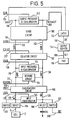
- FIG. 5 illustrates a schematic block diagram of sense circuitry including a dynamic sense amplifier 100 (labelled sense circuit in Figure 5) according to one embodiment of the present invention.
- Each sense amplifier 312a ... 312h can be implemented as such sense circuitry.
- the bit line balancing technique described with reference to Figure 4 is used by way of example, with a cell to be read being in the sub-array 300, the sub-array 302 being used for capacitive balancing. It will be understood that the signal pair being sensed could be otherwise derived, for example a complementary bit line pair as found in SRAMs.
- the sense amplifier comprises a bias/cascode circuit 106 which receives an input on a read line RL 125 of the 8 bit read bus 25 from an accessed cell 2 on a selected bit line 6 of the memory sub-array 300 via a bit line switch and the column decode circuit 304, and an input on a reference read line RRL 126 which is the reference signal REF applied from the reference circuit 308 via one of the switches 321.
- the read reference line RRL is also connected to the corresponding bit line via the bit line switch and the column decode circuit 306, represented by a capacitance C BL formed by a balanced bit line.
- the read line is also connected to the switch 323, which will be an open circuit.
- the bias/cascode circuit 106 also receives a reference voltage VREF on input line 128.
- An input equilibration circuit 146 has a first terminal connected to the read line RL 125, a second terminal connected to the read reference line RRL 126, and is controlled by an equilibration signal EQUIL on line 130.
- the bias/cascode circuit generates a first output AMP1 on a first amplified output line 136 and a second output AMP2 on a second amplified output line 138.
- the amplified outputs AMP1 and AMP2 on lines 136 and 138 form inputs to an isolation circuit 102.
- An input precharge and equilibration circuit 144 has a first terminal connected to the first amplified output AMP1 on line 136, a second terminal connected to the second amplified output terminal AMP2 on line 138, and is controlled by the equilibration signal EQUIL on line 130.
- a restore circuit 104 has a first terminal connected to the first amplified output AMP1 on line 136, a second terminal connected to the second amplified output AMP2 on line 138, and receives a restore control signal RESTORE on line 211.
- the isolation circuit 102 selectively connects the signal AMP1 to a signal output SAIN1 on a first sense input line 150 and the signal AMP2 to a signal output SAIN2 on a second sense input line 152 under the control of an isolation control signal ISOLATE on line 227.
- the sense input lines 150 and 152 form first and second inputs to a dynamic sense amplifier labelled as a sense circuit 100 in figure 5 and referred to accordingly in the following, which additionally receives an activation control signal SENSE on line 154.
- the sense circuit 100 has a first output terminal 156 forming a true output SAOUT , and a second output terminal 158 forming an inverse output NOTSAOUT.
- An output precharge and equilibration circuit 142 has a first terminal connected to the true output SAOUT on line 156, a second terminal connected to the inverse output NOTSAOUT on line 158, and is controlled by the equilibration signal EQUIL.
- a latch 112 receives as inputs the complementary output signals SAOUT and NOTSAOUT on output terminals 156 and 158 and generates an output on line 166 which is one line DB' of the 8 bit databus DB .
- the signal DB' on line 166 forms an input to an output buffer 114 which in turn generates an output OUT on line 168 which is connected to an output pad 116.
- the sense circuit 100 consists of a cross-coupled arrangement of transistors for performing dynamic sensing of a voltage differential on the sense inputs SAIN1 and SAIN2 on lines 150 and 152.
- the cross-coupled arrangement of transistors Prior to applying a differential signal to the inputs of the sense circuit the cross-coupled arrangement of transistors can be held in a meta-stable state until the input differential signal on sense input lines 150 and 152 is sufficient to force the sense circuit into one of its two stable states, namely logic "0" or logic "1" on one output, with the inverse on the other.
- the state of the input differential signal on sense inputs SAIN1 and SAIN2 on lines 150 and 152 is used to determine the logic level on the true output SAOUT on terminal 156 when it changes from its meta-stable state into one of its two stable states.
- the control signal SENSE on line 154 determines when the sense circuit is released from its meta-stable state and allowed to adopt one of its stable states.
- Such cross-coupled transistor arrangements for dynamic sense amplifiers are well known in the art and their operation should be readily understood by a person skilled in the art. A detailed description of a cross-coupled arrangement which may be used in conjunction with a preferred embodiment of the present invention will be given hereinbelow.
- the sense amplifier Prior to the start of the read cycle, the sense amplifier is inactive, and the equilibration control signal EQUIL is set such that the input equilibration circuit 146, input precharge and equilibration circuit 144 and output precharge and equilibration circuit 142 are all switched on.
- the output precharge and equilibration circuit 142 precharges the true output SAOUT and inverse output NOTSAOUT on lines 156 and 158 to a known level, and also clamps the two signal lines together thus forming clamping circuitry.
- the input precharge and equilibration circuit 144 precharges the amplified outputs AMP1 and AMP2 on lines 136 and 138 respectively to a known level, and also clamps the two signal lines together.
- the input equilibration circuit 146 clamps together the signal lines RL and RRL on lines 125 and 126 respectively.
- the signal level of the signals RL and RRL at this stage is determined by the bias/cascode circuit 106.
- the isolation control signal ISOLATE on line 227 is set such that the inputs AMP1 and AMP2 on lines 136 and 138 of the isolation circuit 102 are connected directly to the respective outputs SAIN1 and SAIN2 on lines 150 and 152. Therefore the signals SAIN1 and SAIN2 are clamped together and precharged by the input precharge and equilibration circuit 144 in the same manner as the signals AMP1 and AMP2.
- the restore control signal RESTORE on lines 211 is set at this time such that the restore circuit 104 is disabled.
- the input precharge and equilibration circuitry could be alternatively connected with its first and second terminals connected to the signals SAIN1 and SAIN2 on lines 150 and 152.
- the control signal SENSE on line 154 is set such that the sense circuit 100 is disabled.
- the control signal EQUIL is set to precharge all the signal lines 156,158,150,152,136,138 to a high level.
- the reference signal VREF supplied to the bias/cascode circuit 106 on line 128 is set such that the voltage on the lines 125 and 126 are both identical and are equal to the required bias voltage, namely just less than 1V.
- the voltages on the amplified outputs AMP1 and AMP2 on lines 136 and 138, which are the supply voltage Vcc at this time, provide the potential source for the biasing operation of the bias/cascode circuit 106, the reference signal VREF effectively being a control signal to determine the level of the bias voltage.
- This biasing arrangement for the read line RL and the reference read line RRL , and hence the bit lines, is known for flash memories.
- the selected bit lines are required to be biased to a relatively low voltage, preferably less than 1V during a read operation.
- a relatively low voltage preferably less than 1V during a read operation.
- the majority of operations will be read operations, and it is therefore necessary to minimise the drain stress of the cells on the bit lines during these read operations. If the bit lines were biased to a relatively high voltage the drain stress of the cells may lead to loss of charge from the floating gates of the cells, and consequently partial erasure of programmed cells. Also, such a bias condition may lead to the partial programming of an erased cell.
- a single cell 2 within the memory array 50 is selected to be read, and this cell is connected, via its associated bit line 6 to the read line RL 125 via the switch 304.
- the equilibration signal EQUIL on line 130 changes state such that the input equilibration circuit 144, and the output precharge and equilibration circuit 142 are all disabled. All precharging and clamping then terminates.
- the reference circuit 108 generates the current reference signal REF for comparison with the current signal on the accessed bit line. During a normal read operation the current reference signal REF generated by the reference circuit 108 is equal to half the sum of the currents passed by a programmed cell and an erased cell.
- the reference signal VREF on line 128 is held at the same level, before and throughout a read cycle, to generate the appropriate identical bias voltages on the read line RL 125 and the read reference RRL line 126, provided sufficient potential is provided by the signals AMP1 and AMP2 on lines 136 and 138.
- the voltage on the AMP1 signal line 136 provides the potential for the bias voltage on read line RL 125
- the voltage on the AMP2 signal line 138 provides the potential for the bias voltage on read reference line RRL 126.
- the accessed cell 2 on the selected bit line will typically sink 60 to 100 ⁇ A if erased.
- this small current will only slightly modulate the bias voltage on the read line RL 125, such that there is only a very small voltage difference between the signals on the read RL and read reference RRL lines 125 and 126.
- the bias/cascode circuit 106 acts to amplify the signals on the read and read reference lines 125 and 126 onto the amplified outputs AMP1 and AMP2 on lines 136 and 138 respectively.
- the bias/cascode circuit 106 has a much smaller capacitive loading on its outputs connected to the amplified outputs AMP1 and AMP2 on lines 136 and 138. If all the current flowing in read line 125 flows in the amplified output line 136, and all the current flowing in the read reference line 126 flows in amplified output line 138, this smaller capacitance means that the small voltage differential between the signals RL and RRL on lines 125 and 126 is amplified and appears as a larger voltage differential between the signals AMP1 and AMP2 on lines 136 and 138. The differential voltage signal is therefore amplified before being input to the sense circuit 100.
- the isolation circuit 102 is disabled such that its inputs AMP1 and AMP2 on line 136 and 138 are connected directly to its outputs SAIN1 and SAIN2 on lines 150 and 152 respectively.
- the amplified differential signal appears on the inputs of the sense circuit 100.
- a predetermined time after the read cycle has started the amplified differential signal will have been established on the outputs SAIN2 and SAIN2 on lines 150 and 152, and the control signal SENSE on line 154 changes state such that the cross-couple circuit 100 is released from its meta-stable state, and will be forced, by regenerative action, into one of its two stable states, which one being dependent on the state of the differential signal on its inputs.
- the signal lines RL 125 and RRL 126 are biased to less than 1V.
- the signals AMP1 and AMP2 on lines 136 and 138 are both connected to the supply voltage via the input precharge and equilibration circuit 144, and this provides adequate potential to the bias/cascode circuit 106 for biasing the signals RL and RRL on lines 124 and 126.
- the cross-couple circuit when the cross-couple circuit is enabled and drives its outputs to full CMOS levels, the possibility arises that the potential of one of the signals AMP1 or AMP2 on lines 136 or 138 may fall to a level such that there is insufficient supply for either one of the signals RL or RRL on lines 125 or 126 to be correctly biased.
- the bit line 6 would then need to be precharged or restored to the bias voltage prior to the start of the next read cycle, which is likely to increase the read cycle time.
- the isolation circuit is enabled by the signal ISOLATE on line 227 to disconnect the signals AMP1 and AMP2 on lines 136 and 138 from the signals SAIN1 and SAIN2 on lines 150 and 152 respectively.
- the restore circuit 104 is enabled by the signal RESTORE on line 211. When enabled the restore circuit 104 applies the supply voltage Vcc to the signals AMP1 and AMP2 on the lines 136 and 138 and the correct bias voltage is maintained on the lines RL 125 and RRL 126. Hence during a second stage of the read cycle the restore circuit 104 and the isolation circuit 102 are enabled.
- the dynamic sense amplifier itself drives its outputs to full CMOS levels, then it can be used as a latch.
- the described preferred embodiment has a separate latch device 112 on the output of the dynamic sense amplifier to hold the data value sensed up until the end of the next read cycle.
- the previous data value can be stored whilst the next data value is read, and hence the data hold time of the device is improved.
- the previous data can be held in the separate latch until the new data has been sensed and stored in the separate latch. Without the additional latch 112, the previous data value is lost as soon as the dynamic sense amplifier is precharged ready for the next sense cycle.
- the output DB' of the latch device 112 is connected to an output pad 116 of the memory device via an output buffer 114, as is well know in the art.
- the input equilibration circuit 146 includes a transistor 120 together with transistors 200,202 and 204.
- the transistor 120 has one of its source/drain regions connected to the read line RL 125 and the other of its source/drain regions connected to the read reference line RRL 126.
- the transistor 200 has one of its source/drain regions connected to the read line RL 125 and the other of its source/drain regions connected to one of the source/drain regions of the transistor 202, the transistor 202 having the other of its source/drain regions connected to the read reference line RRL 126.
- the transistors 120,200 and 202 all have their gates connected to the control signal EQUIL on line 130.
- the transistor 204 is connected in a diode configuration with its gate connected to the common source/drain regions of the transistors 200 and 202, one of its source/drain regions connected to its gate, and the other of its : source/drain regions connected to the lower supply rail (normally at ground voltage). This transistor 204 ensures correct bias at the read line RL and the read reference line RRL during the precharge phase.
- the bias/cascode circuit 106 comprises a first n-type source-follower transistor 206 having its source connected to the read line RL 125 and its drain connected to the signal AMP1 on line 136, and a second n-type source-follower transistor 108 having its source connected to the read reference line RRL 126 and its drain connected to the signal AMP2 on line 138.
- the gates of the transistors 206 and 108 are both connected to the reference voltage VREF on line 128.
- the restore circuit 104 comprises a first p-type transistor 210 having its source connected to the supply voltage and its drain connected to the signal AMP1 on line 136, and a second p-type transistor 212 having its source connected to the supply voltage and its drain connected to the signal AMP2 on line 138. Because the restore circuit 104 is implemented with p-channel transistor devices in the preferred embodiment, the gates of the p-channel transistors 210 and 212 are both connected to the inverse of the restoration control signal NOTRESTORE on line 254.
- the input precharge and equilibration circuit 144 comprises only a p-channel equilibration transistor 118 in the preferred embodiment, having one of its source/drain regions connected to the signal AMP1 on line 136 and the other of its source/drain regions connected to the signal AMP2 on line 138. Because the equilibration transistor 118 is a p-channel device, its gate is connected to the inverse of the equilibration control signal NOTEQUIL on line 160.
- the input precharge and equilibration circuit 144 is not provided with any precharge circuitry in the preferred embodiment since, as will become apparent in the following description of the preferred embodiment of the sense circuit 100, in the prefered dynamic sense amplifier the output SAOUT on line 156 is connected directly to the input SAIN1 on line 150, and the output NOTSAOUT on line 158 is connected directly to the input SAIN2 on line 152.
- the output equilibration and precharge circuit 142 can therefore precharge the signals SAIN1 and SAIN2, AMP1 and AMP2 as well as the signals SAOUT and NOTSAOUT.
- it will be apparent to a person skilled in the art having reference to the following description of the output precharge and equilibration circuit 142 how the input precharge and equilibration circuit 144 could be adapted to include precharge devices if necessary.
- the isolation circuit 102 comprises two n-type transistors 214 and 220 and two p-type transistors 216 and 218.
- the transistors 214 and 220 each have their respective sources connected to the signals AMP1 and AMP2 on lines 136 and 138 respectively, and their respective drains connected to the outputs SAIN1 and SAIN2 on lines 150 and 152 respectively.
- the transistors 216 and 218 each have their respective sources connected to the outputs SAIN1 and SAIN2 on lines 150 and 152 respectively and their respective drains connected to the signals AMP1 and AMP2 on lines 136 and 138 respectively.
- the gates of transistors 214 and 220 are connected to the sensing signal NOTSENSE on line 226 which is derived from the output of an inverter 222, the inverter receiving at its input the signal SENSE on line 154.
- the gates of the transistors 216 and 218 are connected to the isolation signal ISOLATE on line 227.
- the output precharge and equilibration circuit 142 comprises three p-channel transistors 122,232 and 234.
- the p-channel transistor 232 has its source connected to the supply voltage and its drain connected to the true output SAOUT on the output terminal 156.
- the p-channel transistor 234 has its source connected to the supply voltage and its drain connected to the inverse output NOTSAOUT on output terminal 158.
- the p-channel transistor 122 has one of its source/drain regions connected to the output SAOUT on output terminal 156 and the other of its source/drain regions connected to the output NOTSAOUT on output terminal 158.
- the gates of the p-channel transistors 122,232 and 234 are all connected to the signal NOTEQUIL on line 160.
- the sense circuit 100 senses a voltage differential on its inputs and comprises cross-coupled transistors 236,238,240,242.
- the cross-coupled transistor 236 has its source connected to the supply voltage, its drain connected to the true output SAOUT on output terminal 156, and its gate connected to the inverse output NOTSAOUT on output terminal 158.
- the cross-coupled transistor 238 has its source connected to the supply voltage, its drain connected to the inverse output NOTSAOUT on output terminal 158, and its gate connected to the true output SAOUT on output terminal 156.
- the transistor 240 has its drain region connected to the true output SAOUT on output terminal 156, its source connected to the signal SENSE on line 226, and its gate connected to the inverse output NOTSAOUT on output terminal 158.
- the transistor 242 has its drain connected to the inverse output NOTSAOUT on output terminal 158, its source connected to the signal SENSE on line 226, and its gate connected to the true output SAOUT on output terminal 156.
- the transistors 206 and 208 of the bias/cascode circuit 106 are biased in source-follower configuration, and therefore the potential of the source of either of these two transistors will be equal to the potential at their respective gates less the threshold voltage, Vtn, of the device. As was described hereinabove with reference to Figure 5, it is desired to bias the read and read reference lines 125 and 126 to a value of less than 1V.
- the threshold voltage Vtn of each of the two transistors 206,208 will be typically 0.8V.
- the reference signal VREF is fixed to a value of twice the threshold voltage Vtn, provided a sufficient voltage is supplied to the drains of the transistors 206 and 208 the read and read reference lines 125 and 126 will both be biased to the value Vtn, which is as required.
- the signal NOTEQUIL on line 160 Prior to a read cycle, the signal NOTEQUIL on line 160 is low, and hence the p-type transistors 122,232 and 234 are all switched on. These three transistors precharge the outputs SAOUT and NOTSAOUT on output terminals 156 and 158 of the dynamic sense amplifier to the supply voltage Vcc and also clamp the two output terminals together. At this time the signal EQUIL on line 130 is high and the transistor 120 is switched on to clamp the read line RL 125 and the read reference line RRL 126 together.
- the sense clock signal SENSE on line 154 is low, such that the signal NOTSENSE on line 226 is high and the sense circuit 100 is therefore disabled since the signals SAIN1, SAIN2 and SENSE on the lines 150,152 and 226 respectively are all at the supply voltage. As the signal SENSE on line 226 is high, the n-channel transistors 214 and 220 are switched on. Furthermore, the signal ISOLATE on line 227 is low such that the p-channel transistors 216 and
- the signals AMP1 and AMP2 on lines 136 and 138 are also clamped to the supply voltage, and furthermore are clamped together by the p-channel transistor 118.
- the signal NOTRESTORE on line 211 is high such that the transistors 210 and 212 are switched off.
- the reference signal VREF on line 128 is permanently held at a value equal to twice the threshold voltage of the transistors 206 and 208 during a read cycle. It will be understood, however, that if a separate precharge circuit was required for the signals AMP1 and AMP2, because the outputs of the sense circuit 100 were not connected to their respective inputs, the restore devices 210 and 212 could be enabled to provide precharge. This could be achieved by appropriate gating of the signal NOTRESTORE with the signal NOTEQUIL .
- the control circuit of Figure 7 comprises three two-input NAND gates 400 to 404 and a plurality of inverters 406 to 416.
- the control circuit receives as inputs a global sense signal GLSEN on line 420, a selection signal SELECT on line 422, and an enable signal START on line 424.
- the control circuit generates the inverse of the restoration signal NOTRESTOR E on line 254, the isolation signal ISOLATE on line 227, the sensing signal SENSE on line 154, the equilibration signal EQUIL on line 130, and the inverse of the equilibration signal NOTEQUIL on line 140.
- the NAND gate 404 receives as inputs the signals SELECT and START .
- the NAND gate 400 receives as inputs the signal GLSEN and the otuput of the NAND gate 404 inverted by the inverter 408.
- the NAND gate 402 receives as inputs the output of the NAND gate 400 inverted by the inverter 406 and the output of the NAND gate 404 via the inverter 408.
- the signal NOTRESTORE is derived from the output of the NAND gate 402 inverted successively by the inverters 410 and 416.
- the signal RESTORE is derived from the output of the NAND gate 402 inverted by the inverter 410.
- the signal SENSE is derived from the output of the NAND gate 400 inverted by the inverter 406.
- the signal EQUIL is derived from the output of the NAND gate 404 inverted successively by the inverters 408 and 412.
- the signal NOTEQUIL is derived from the output of the NAND gate 404 inverted successively by the inverters 408,412 and 414.
- the signal SELECT on line 422 is a signal that enables the control circuit on a memory device divided into a plurality of sub-arrays, each sub-array having a plurality (in this embodiment eight) of sense amplifiers.
- the signal SELECT will be set if that sub-array with which the control circuit is associated is selected for operation.
- the signal START is a control signal which allows the read cycle to commence and hence the precharge and equilibration circuitry is disabled in response to the signal START . In the preferred embodiment the signal START becomes active in response to the selected wordline becoming active.
- the signal GLSEN which is applied to all the sense amplifiers in the memory device controls the timing of the clocking of the sense circuit.
- the signal GLSEN is timed to become active a fixed time after the read cycle becomes active in response to the signal START becoming active.
- the signal EQUIL goes low and the signal NOTEQUIL goes high.
- a differential signal will develop between the read line RL 125 and the read reference line RRL 126, the state of which will depend on whether the cell accessed in the selected bit line is programmed or erased.
- the source-follower transistors 206 and 208 now act as cascode devices to amplify the voltage signals on their respective sources onto their respective drains.
- the voltage differential on the drains of the transistors 206 and 208 will be much greater than that on their respective sources, since the capacitance on the drain side is much lower than the capacitance on the source side as explained hereinabove with reference to Figure 5.
- the transistors 214,216,218 and 220 are all switched on, the voltage differential developed between the drains of the transistors 206 and 208 is also developed between the inputs SAIN1 and SAIN2 and therefore the complementary outputs SAOUT and NOTSAOUT on lines 156 and 158 respectively.
- the time period between releasing the precharge and equilibration devices and releasing the cross-couple circuits is called the integration period. This period is so-called because the voltage change on a node (in this case each sense amplifier output) over a period of time is equal to the integral of the current through the node over that period of time divided by the capacitance associated with that node.
- V(SAOUT) - V(NOTSAOUT) 1 C [i(cell) - i(ref)] .dt
- C the capacitance associated with each output node of the sense amplifier (assumed to be identical)
- i(cell) is the current due to the cell being read
- i(ref) is the current due to the reference signal REF .
- the signals SAIN1 and SAIN2 on lines 150 and 152 are isolated from the signals AMP1 and AMP2 on lines 136 and 138 respectively.
- the capacitance of the read RL and read reference RRL lines 125 and 126 is therefore isolated from the output terminals 156,158 of the dynamic sense amplifier so that the outputs are able to settle at their final value more quickly.
- the signal NOTRESTORE going low causes the p-channel transistors 210 and 212 to switch on, so that the signals AMP1 and AMP2 on lines 136 and 138 are maintained at the potential of the supply voltage.
- the operation of the source-follower transistors 206 and 208, to ensure a bias voltage equal to the threshold voltage of these transistors on the read line RL 125 and the read reference line RRL 126 is maintained. If the correct bias voltage on the read line RL 125 and the read reference line RRL 126 was not maintained in this way, any potential on the read line or bit line may slowly discharge to ground via cell currents, and any potential on the read reference line may slowly discharge to ground via reference currents. Therefore these lines would need to be restored prior to a subsequent sense operation.
- the data outputs on the outputs SAOUT and NOTSAOUT can be latched into a latch such as described hereinabove with reference to Figure 4.
- the signals SENSE, ISOLATE, NOTRESTORE, NOTEQUIL and EQUIL can then be forced to their original states, ready for the next sensing operation.
- FIG. 8 shows the timing relationship of selected signals of the sense circuit during a read cycle as described in detail hereinabove.
- the timing diagram shows the precharge/equilibration period during the beginning of the read cycle controlled by the signal EQUIL being high, the subsequent integration period when the signal EQUIL goes low and the outputs SAOUT and NOTSAOUT begin to move apart, the sense period after the signal SENSE goes high and the signals SAOUT and NOTSAOUT move to opposite CMOS logic levels, and the further precharge/equilibration period after the signal EQUIL returns high and the signal SENSE returns low, the signals SAOUT and NOTSAOUT returning to their precharged level of Vcc .
Landscapes
- Read Only Memory (AREA)
Claims (15)
- Integrierte Speicherschaltungsanordnung, mit:dadurch gekennzeichnet, daß die Leseschaltung aufweist:einer Matrix (50) von Speicherzellen (2), die in Zeilen und Spalten angeordnet ist, wobei die Zellen in einer Zeile mit einer gemeinsamen Wortleitung (8) und die Zellen in einer Spalte mit einer gemeinsamen Bitleitung (6) verbunden sind, wobei jede Speicherzelle (2) einen Floating-Gate (FG) Transistor (4) aufweist, der ein Datenbit speichert, wobei die integrierte Speicherschaltungsanordnung ferner aufweist:Leseschaltung (29) zum Lesen eines Datenbit, welches in einer ausgewählten der Speicherzellen gespeichert ist;Umschaltschaltung (31, 57) zum Verbinden der der ausgewählten Speicherzelle (2) zugehörigen Bitleitung (6) mit der Leseschaltung (29);einen dynamischen Leseverstärker (100) mit einem ersten und zweiten Eingangsanschluß (150, 152) zur Verbindung mit der ausgewählten Bitleitung (6) bzw. einem Referenzsignal (REF) und einem ersten und einem zweiten Ausgangsanschluß (156, 158), wobei der dynamische Leseverstärker (100) auch eine Latchschaltung (236, 238, 240, 242) zum Treiben des ersten und zweiten Ausgangsanschlusses (156, 158) auf entgegengesetzte logische Zustände in Abhängigkeit von dem Differenzzustand zwischen einem Signal auf der ausgewählten Bitleitung (6) und dem Referenzsignal (REF) umfaßt, wobei einer der logischen Zustände durch eine Versorgungsspannung (Vcc) des dynamischen Leseverstärkers bestimmt wird;Begrenzungsschaltung (142), welche mit dem ersten und zweiten Ausgangsanschluß (156, 158) verbunden ist, um diese auf einem gemeinsamen Vorladesignalpegel zu halten, und welche ein Freigabesignal (130) zur Freigabe des ersten und zweiten Ausgangsanschlusses empfängt;Vorspannungsschaltung (106), welche zwischen dem dynamischen Leseverstärker und der ausgewählten Bitleitung verbunden ist, um die ausgewählte Bitleitung (6) auf einen vorgegebenen Spannungspegel vorzuspannen;Rückstellschaltung (104), welche zwischen der Vorspannungsschaltung (106) und dem dynamischen Leseverstärker (100) verbunden ist, um selektiv die Vorspannungsschaltung (106) mit der Versorgungsspannung (Vcc) zu verbinden;Trennschaltung (102), welche zwischen dem dynamischen Leseverstärker (100) und der Vorspannungsschaltung (106) verbunden ist und während einer ersten Stufe eines Lesezyklus betreibbar ist, um einen ersten Zustand anzunehmen, um die Vorspannungsschaltung (106) mit dem dynamischen Leseverstärker (100) zu verbinden, und ein Trennsignal (227) empfängt, um einen zweiten Zustand in einer zweiten Stufe des Lesezyklus anzunehmen, wobei die Vorspannungsschaltung (106) von dem dynamischen Leseverstärker (100) getrennt ist, die Vorspannungsschaltung (106) mit der Versorgungsspannung (Vcc) über die Rückstellschaltung (104) verbunden ist, wenn sich die Trennschaltung (102) im zweiten Zustand befindet.
- Integrierte Speicherschaltungsanordnung nach Anspruch 1, bei welcher, wenn die Trennschaltung (102) sich im ersten Zustand befindet, die Vorspannungsschaltung (106) mit der Versorgungsspannung über die Latchschaltung (236, 238, 240, 242) verbunden ist und die Ausgangssignale auf einem gemeinsamen Vorladesignalpegel gehalten werden.
- Integrierte Speicherschaltungsanordnung nach Anspruch 1, bei welcher, wenn die Trennschaltung (102) sich im ersten Zustand befindet, die Vorspannungsschaltung (106) mit der Versorgungsspannung über eine Eingang-Vorladeschaltung (144) verbunden ist, und die Ausgangssignale auf einem gemeinsamen Vorladesignalpegel gehalten werden.
- Integrierte Speicherschaltungsanordnung nach Anspruch 3, bei welcher die Rückstellschaltung (104) die Vorspannungsschaltung bereitstellt.
- Integrierte Speicherschaltungsanordnung nach einem der vorstehenden Ansprüche, bei welcher jede Speicherzelle (2) einen Einzeltransistor (4) umfaßt.
- Integrierte Speicherschaltungsanordnung nach Anspruch 5, bei welcher der Einzeltransistor (4) ein elektrisch programmierbarer Floating-Gate (FG) Transistor ist.
- Integrierte Speicherschaltungsanordnung nach einem der vorstehenden Ansprüche, bei welcher die Vorspannungsschaltung (106) zur Verstärkung der Differenz zwischen dem Signal auf der ausgewählten Bitleitung (6) und dem Referenzsignal (REF) während des Lesens dient.
- Integrierte Speicherschaltungsanordnung nach einem der vorstehenden Ansprüche, bei welcher die Vorspannungsschaltung (106) einen ersten und zweiten Vorspannungstransistor (206, 208) aufweist, welche jeweils einen Steuerungsanschluß aufweisen, der angeschlossen ist, um eine Referenzspannung (VREF) auf einem Pegel zu empfangen, um die Transistoren in einem leitenden Zustand zu halten, und einen steuerbaren Pfad, der jeweils zwischen der ausgewählten Bitleitung und der Referenzspannung sowie der Trennschaltung (102) angeschlossen ist.
- Integrierte Speicherschaltungsanordnung nach Anspruch 8, bei welcher die Rückstellschaltung (104) einen ersten und zweiten Rückstelltransistor (210, 212) aufweist, welche jeweils einen Steuerungsanschluß aufweisen, der verbunden ist, um ein Rückstellsignal zu empfangen, und einen steuerbaren Pfad, der zwischen der Versorgungsspannung und dem ersten und zweiten Vorspannungstransistor (206, 208) angeschlossen ist, wobei das Rückstellsignal die Rückstelltransistoren aktiviert, wenn die Trennschaltung (102) sich im zweiten Zustand befindet.
- Integrierte Speicherschaltungsanordnung nach einem der vorstehenden Ansprüche, bei welcher die Versorgungsspannung 3.3V±.3V beträgt.
- Integrierte Speicherschaltungsanordnung nach einem der Ansprüche 1 bis 6, bei welcher die Versorgungsspannung 5V±.5V beträgt.
- Integrierte Speicherschaltungsanordnung nach einem der vorstehenden Ansprüche, bei welcher das Referenzsignal (REF) durch eine Referenzschaltung (308) zugeführt wird, welche mit einer Kapazität verbunden ist, die angeordnet ist, um mit der Kapazität der ausgewählten Bitleitung übereinzustimmen.
- Integrierte Speicherschaltungsanordnung nach Anspruch 12, welche eine weitere Matrix (302) von Speicherzellen umfaßt, die in Zeilen und Spalten angeordnet sind, wobei die Zellen in einer Spalte mit einer gemeinsamen weiteren Bitleitung verbunden sind, wobei jede Speicherzelle ein Datenbit speichert; und welche ferner eine Umschaltschaltung (310) zum Verbinden einer weiteren Bitleitung (322a-322h), welche der der ausgewählten Speicherzelle zugeordneten Bitleitung (320a-320h) entspricht, mit der Referenzschaltung (308), wobei die entsprechende Bitleitung eine übereinstimmende Kapazität bereitstellt.
- Integrierte Speicherschaltungsanordnung nach Anspruch 12 oder 13, bei welcher die Referenzschaltung einen Konstantschaltungsgenerator zum Erzeugen eines Referenzsignals umfaßt.
- Integrierte Speicherschaltungsanordnung nach einem der vorstehenden Ansprüche, bei welcher die Leseschaltung eine Mehrzahl von dynamischen Leseverstärkern (312a-312h) aufweist und zugehörige Begrenzungsschaltungen, Vorspannungsschaltungen und Trennschaltungen.
Applications Claiming Priority (2)
| Application Number | Priority Date | Filing Date | Title |
|---|---|---|---|
| GB9423036 | 1994-11-15 | ||
| GB9423036A GB9423036D0 (en) | 1994-11-15 | 1994-11-15 | An integrated circuit memory device |
Publications (2)
| Publication Number | Publication Date |
|---|---|
| EP0713222A1 EP0713222A1 (de) | 1996-05-22 |
| EP0713222B1 true EP0713222B1 (de) | 2002-02-13 |
Family
ID=10764430
Family Applications (1)
| Application Number | Title | Priority Date | Filing Date |
|---|---|---|---|
| EP95307998A Expired - Lifetime EP0713222B1 (de) | 1994-11-15 | 1995-11-09 | Integrierte Speicherschaltungsanordnung |
Country Status (5)
| Country | Link |
|---|---|
| US (1) | US5764572A (de) |
| EP (1) | EP0713222B1 (de) |
| JP (1) | JPH08227586A (de) |
| DE (1) | DE69525421D1 (de) |
| GB (1) | GB9423036D0 (de) |
Families Citing this family (71)
| Publication number | Priority date | Publication date | Assignee | Title |
|---|---|---|---|---|
| US20050281887A1 (en) * | 1995-08-31 | 2005-12-22 | Rizoiu Ioana M | Fluid conditioning system |
| KR100248868B1 (ko) * | 1996-12-14 | 2000-03-15 | 윤종용 | 플래시 불휘발성 반도체 메모리 장치 및 그 장치의 동작 모드 제어 방법 |
| IT1291283B1 (it) * | 1997-04-30 | 1999-01-07 | Sgs Thomson Microelectronics | Amplificatore di lettura dinamico per dispositivi di memoria a semiconduttore di tipo eprom eeprom e flash-eprom |
| US5831895A (en) * | 1997-07-30 | 1998-11-03 | Micron Technology, Inc. | Dynamic cell plate sensing and equilibration in a memory device |
| KR100327421B1 (ko) * | 1997-12-31 | 2002-07-27 | 주식회사 하이닉스반도체 | 비휘발성 메모리 소자의 프로그램 시스템 및 그의 프로그램 방법 |
| US6108240A (en) * | 1999-02-04 | 2000-08-22 | Tower Semiconductor Ltd. | Implementation of EEPROM using intermediate gate voltage to avoid disturb conditions |
| US6259643B1 (en) * | 1999-05-28 | 2001-07-10 | Systems Integration Inc. | Single event upset (SEU) hardened static random access memory cell |
| US6816554B1 (en) * | 1999-07-12 | 2004-11-09 | Intel Corporation | Communication bus for low voltage swing data signals |
| US6678196B2 (en) * | 2001-07-06 | 2004-01-13 | Micron Technology, Inc. | Writing to and reading from a RAM or a CAM using current drivers and current sensing logic |
| US6618307B2 (en) * | 2001-09-05 | 2003-09-09 | Sun Microsystems, Inc. | Dynamic DRAM sense amplifier |
| US6525982B1 (en) * | 2001-09-11 | 2003-02-25 | Micron Technology, Inc. | Methods of programming and circuitry for a programmable element |
| KR100454143B1 (ko) * | 2001-11-19 | 2004-10-26 | 주식회사 하이닉스반도체 | 플래쉬 메모리 소자 및 그 소거 방법 |
| US7061792B1 (en) * | 2002-08-10 | 2006-06-13 | National Semiconductor Corporation | Low AC power SRAM architecture |
| KR100484255B1 (ko) * | 2002-10-31 | 2005-04-22 | 주식회사 하이닉스반도체 | 감지증폭기의 동작시 노이즈가 감소된 반도체 메모리 장치 |
| US6812746B2 (en) * | 2002-11-12 | 2004-11-02 | Micron Technology, Inc. | Method and apparatus for amplifying a regulated differential signal to a higher voltage |
| US6768677B2 (en) * | 2002-11-22 | 2004-07-27 | Advanced Micro Devices, Inc. | Cascode amplifier circuit for producing a fast, stable and accurate bit line voltage |
| FR2859327B1 (fr) * | 2003-08-29 | 2005-11-25 | St Microelectronics Sa | Dispositif de commutation permettant de commuter un noeud sur plusieurs potentiels sans courant de croisement |
| US7164612B1 (en) * | 2003-10-10 | 2007-01-16 | Sun Microsystems, Inc. | Test circuit for measuring sense amplifier and memory mismatches |
| DE10355320B3 (de) * | 2003-11-27 | 2005-04-14 | Infineon Technologies Ag | Hochauflösender digitaler Pulsweitenmodulator und Verfahren zum Erzeugen eines hochaufgelösten pulsweitenmodulierten Signals |
| KR100598167B1 (ko) * | 2004-02-05 | 2006-07-10 | 주식회사 하이닉스반도체 | 반도체 메모리 장치 및 센스앰프의 접속방법 |
| US7187585B2 (en) * | 2005-04-05 | 2007-03-06 | Sandisk Corporation | Read operation for non-volatile storage that includes compensation for coupling |
| US7196928B2 (en) * | 2005-04-05 | 2007-03-27 | Sandisk Corporation | Compensating for coupling during read operations of non-volatile memory |
| US7196946B2 (en) * | 2005-04-05 | 2007-03-27 | Sandisk Corporation | Compensating for coupling in non-volatile storage |
| US7366022B2 (en) * | 2005-10-27 | 2008-04-29 | Sandisk Corporation | Apparatus for programming of multi-state non-volatile memory using smart verify |
| US7301817B2 (en) * | 2005-10-27 | 2007-11-27 | Sandisk Corporation | Method for programming of multi-state non-volatile memory using smart verify |
| US7349258B2 (en) * | 2005-12-06 | 2008-03-25 | Sandisk Corporation | Reducing read disturb for non-volatile storage |
| US7262994B2 (en) * | 2005-12-06 | 2007-08-28 | Sandisk Corporation | System for reducing read disturb for non-volatile storage |
| US7443726B2 (en) * | 2005-12-29 | 2008-10-28 | Sandisk Corporation | Systems for alternate row-based reading and writing for non-volatile memory |
| US7349260B2 (en) * | 2005-12-29 | 2008-03-25 | Sandisk Corporation | Alternate row-based reading and writing for non-volatile memory |
| US7436733B2 (en) * | 2006-03-03 | 2008-10-14 | Sandisk Corporation | System for performing read operation on non-volatile storage with compensation for coupling |
| US7499319B2 (en) * | 2006-03-03 | 2009-03-03 | Sandisk Corporation | Read operation for non-volatile storage with compensation for coupling |
| US7440331B2 (en) * | 2006-06-01 | 2008-10-21 | Sandisk Corporation | Verify operation for non-volatile storage using different voltages |
| US7457163B2 (en) * | 2006-06-01 | 2008-11-25 | Sandisk Corporation | System for verifying non-volatile storage using different voltages |
| US7310272B1 (en) * | 2006-06-02 | 2007-12-18 | Sandisk Corporation | System for performing data pattern sensitivity compensation using different voltage |
| US7450421B2 (en) * | 2006-06-02 | 2008-11-11 | Sandisk Corporation | Data pattern sensitivity compensation using different voltage |
| US7352628B2 (en) * | 2006-06-19 | 2008-04-01 | Sandisk Corporation | Systems for programming differently sized margins and sensing with compensations at select states for improved read operations in a non-volatile memory |
| US7606084B2 (en) * | 2006-06-19 | 2009-10-20 | Sandisk Corporation | Programming differently sized margins and sensing with compensations at select states for improved read operations in non-volatile memory |
| US7495953B2 (en) * | 2006-07-20 | 2009-02-24 | Sandisk Corporation | System for configuring compensation |
| US7443729B2 (en) * | 2006-07-20 | 2008-10-28 | Sandisk Corporation | System that compensates for coupling based on sensing a neighbor using coupling |
| US7400535B2 (en) * | 2006-07-20 | 2008-07-15 | Sandisk Corporation | System that compensates for coupling during programming |
| US7885119B2 (en) * | 2006-07-20 | 2011-02-08 | Sandisk Corporation | Compensating for coupling during programming |
| US7506113B2 (en) * | 2006-07-20 | 2009-03-17 | Sandisk Corporation | Method for configuring compensation |
| US7522454B2 (en) * | 2006-07-20 | 2009-04-21 | Sandisk Corporation | Compensating for coupling based on sensing a neighbor using coupling |
| US7684247B2 (en) * | 2006-09-29 | 2010-03-23 | Sandisk Corporation | Reverse reading in non-volatile memory with compensation for coupling |
| US7447076B2 (en) * | 2006-09-29 | 2008-11-04 | Sandisk Corporation | Systems for reverse reading in non-volatile memory with compensation for coupling |
| US7616498B2 (en) * | 2006-12-29 | 2009-11-10 | Sandisk Corporation | Non-volatile storage system with resistance sensing and compensation |
| US7518923B2 (en) * | 2006-12-29 | 2009-04-14 | Sandisk Corporation | Margined neighbor reading for non-volatile memory read operations including coupling compensation |
| US7606070B2 (en) * | 2006-12-29 | 2009-10-20 | Sandisk Corporation | Systems for margined neighbor reading for non-volatile memory read operations including coupling compensation |
| US7590002B2 (en) * | 2006-12-29 | 2009-09-15 | Sandisk Corporation | Resistance sensing and compensation for non-volatile storage |
| US7440324B2 (en) * | 2006-12-29 | 2008-10-21 | Sandisk Corporation | Apparatus with alternating read mode |
| US7495962B2 (en) * | 2006-12-29 | 2009-02-24 | Sandisk Corporation | Alternating read mode |
| US7535764B2 (en) * | 2007-03-21 | 2009-05-19 | Sandisk Corporation | Adjusting resistance of non-volatile memory using dummy memory cells |
| KR100854908B1 (ko) * | 2007-03-29 | 2008-08-28 | 주식회사 하이닉스반도체 | 반도체 메모리 소자의 셀 어레이 및 이의 동작 방법 |
| US7751253B2 (en) | 2008-03-17 | 2010-07-06 | Micron Technology, Inc. | Analog sensing of memory cells with a source follower driver in a semiconductor memory device |
| US7848144B2 (en) * | 2008-06-16 | 2010-12-07 | Sandisk Corporation | Reverse order page writing in flash memories |
| US7755946B2 (en) * | 2008-09-19 | 2010-07-13 | Sandisk Corporation | Data state-based temperature compensation during sensing in non-volatile memory |
| FR2948809B1 (fr) * | 2009-07-31 | 2012-08-17 | St Microelectronics Rousset | Amplificateur de lecture faible puissance auto-minute |
| FR2951575B1 (fr) * | 2009-10-20 | 2011-12-16 | St Microelectronics Rousset | Amplificateur de lecture ayant des moyens de precharge de bitline rapides |
| US9847666B2 (en) | 2013-09-03 | 2017-12-19 | Apple Inc. | Power management for inductive charging systems |
| JP6161482B2 (ja) | 2013-09-19 | 2017-07-12 | ルネサスエレクトロニクス株式会社 | 半導体記憶装置 |
| US9837866B2 (en) | 2013-10-09 | 2017-12-05 | Apple Inc. | Reducing power dissipation in inductive energy transfer systems |
| US9673784B2 (en) * | 2013-11-21 | 2017-06-06 | Apple Inc. | Using pulsed biases to represent DC bias for charging |
| US9123414B2 (en) * | 2013-11-22 | 2015-09-01 | Micron Technology, Inc. | Memory systems and memory programming methods |
| US9336875B2 (en) | 2013-12-16 | 2016-05-10 | Micron Technology, Inc. | Memory systems and memory programming methods |
| US10122217B2 (en) | 2015-09-28 | 2018-11-06 | Apple Inc. | In-band signaling within wireless power transfer systems |
| US10248499B2 (en) | 2016-06-24 | 2019-04-02 | Sandisk Technologies Llc | Non-volatile storage system using two pass programming with bit error control |
| US10601250B1 (en) | 2016-09-22 | 2020-03-24 | Apple Inc. | Asymmetric duty control of a half bridge power converter |
| US10366752B2 (en) * | 2016-12-11 | 2019-07-30 | Technion Research & Development Foundation Ltd. | Programming for electronic memories |
| US10978899B2 (en) | 2017-02-02 | 2021-04-13 | Apple Inc. | Wireless charging system with duty cycle control |
| KR102689654B1 (ko) | 2019-07-10 | 2024-07-31 | 삼성전자주식회사 | 메모리 장치 |
| CN118038941A (zh) * | 2024-03-20 | 2024-05-14 | 北京超弦存储器研究院 | 感应放大器及其感测方法、存储装置及其数据读取方法、电子设备 |
Family Cites Families (14)
| Publication number | Priority date | Publication date | Assignee | Title |
|---|---|---|---|---|
| JPS61184794A (ja) * | 1985-02-13 | 1986-08-18 | Toshiba Corp | 半導体記憶装置 |
| JPS6363197A (ja) * | 1986-09-03 | 1988-03-19 | Toshiba Corp | 半導体記憶装置 |
| US4980863A (en) * | 1987-03-31 | 1990-12-25 | Kabushiki Kaisha Toshiba | Semiconductor memory device having switching circuit for coupling together two pairs of bit lines |
| US5088065A (en) * | 1987-09-04 | 1992-02-11 | Hitachi, Ltd. | Static type semiconductor memory |
| EP0329910B1 (de) * | 1988-02-26 | 1991-05-29 | International Business Machines Corporation | Zweistufiger Leserverstärker für RAM-Speicher |
| JPH01277396A (ja) * | 1988-04-28 | 1989-11-07 | Mitsubishi Electric Corp | 不揮発性半導体記憶装置 |
| US5022009A (en) * | 1988-06-02 | 1991-06-04 | Mitsubishi Denki Kabushiki Kaisha | Semiconductor memory device having reading operation of information by differential amplification |
| JP2621411B2 (ja) * | 1988-08-31 | 1997-06-18 | 三菱電機株式会社 | 不揮発性半導体記憶装置 |
| JPH0411397A (ja) * | 1990-04-27 | 1992-01-16 | Mitsubishi Electric Corp | 不揮発性半導体記憶装置 |
| JPH0411396A (ja) * | 1990-04-27 | 1992-01-16 | Mitsubishi Electric Corp | 不揮発性半導体記憶装置 |
| JPH04119597A (ja) * | 1990-09-07 | 1992-04-21 | Mitsubishi Electric Corp | 不揮発性半導体記憶装置のセンスアンプ |
| JP2509004B2 (ja) * | 1991-03-04 | 1996-06-19 | 株式会社東芝 | 半導体記憶装置 |
| DE69222712T2 (de) * | 1991-07-25 | 1998-02-12 | St Microelectronics Srl | Leseverstärker für programmierbare Speicher mit einer virtuell verbesserten Signalquelle |
| JP3142335B2 (ja) * | 1991-09-24 | 2001-03-07 | 株式会社東芝 | 不揮発性半導体記憶装置 |
-
1994
- 1994-11-15 GB GB9423036A patent/GB9423036D0/en active Pending
-
1995
- 1995-11-09 EP EP95307998A patent/EP0713222B1/de not_active Expired - Lifetime
- 1995-11-09 DE DE69525421T patent/DE69525421D1/de not_active Expired - Lifetime
- 1995-11-15 JP JP29652695A patent/JPH08227586A/ja active Pending
-
1997
- 1997-06-03 US US08/868,478 patent/US5764572A/en not_active Expired - Lifetime
Also Published As
| Publication number | Publication date |
|---|---|
| US5764572A (en) | 1998-06-09 |
| EP0713222A1 (de) | 1996-05-22 |
| GB9423036D0 (en) | 1995-01-04 |
| JPH08227586A (ja) | 1996-09-03 |
| DE69525421D1 (de) | 2002-03-21 |
Similar Documents
| Publication | Publication Date | Title |
|---|---|---|
| EP0713222B1 (de) | Integrierte Speicherschaltungsanordnung | |
| EP0713164B1 (de) | Referenzschaltung | |
| JP3373632B2 (ja) | 不揮発性半導体記憶装置 | |
| US5455786A (en) | Ferroelectric memory | |
| US5677865A (en) | Ferroelectric memory using reference charge circuit | |
| US7855583B2 (en) | Sense amplifier for low voltage high speed sensing | |
| US5574679A (en) | Memory data protection for a ferroelectric memory | |
| US6999365B2 (en) | Semiconductor memory device and current mirror circuit | |
| US6052307A (en) | Leakage tolerant sense amplifier | |
| US5220527A (en) | Dynamic type semiconductor memory device | |
| JPH10340588A (ja) | 不揮発性メモリ装置及びその記入方法 | |
| KR0184088B1 (ko) | 반도체기억장치 | |
| JPH087997B2 (ja) | ランダムアクセスメモリ装置 | |
| US6208550B1 (en) | Ferroelectric memory device and method for operating thereof | |
| US6104635A (en) | Non-volatile memory device readable write data latch, and internal control thereof | |
| JPH081749B2 (ja) | ダイナミックランダムアクセスメモリ装置 | |
| EP0713223B1 (de) | Lesen einer Bitleitung in einer Speichermatrix | |
| US5726936A (en) | Controlling capacitive load | |
| JP3825596B2 (ja) | 半導体記憶装置及びその制御方法 | |
| JP4680195B2 (ja) | 半導体装置及びソース電圧制御方法 | |
| US6295223B1 (en) | Ferroelectric random access memory with a memory with a stable sensing margin | |
| US5295099A (en) | Dynamic random access memory device having static column mode of operation without destruction of data bit | |
| KR0167681B1 (ko) | 클램프 회로를 구비한 반도체 메모리 장치의 센스앰프 구동회로 | |
| JP2643298B2 (ja) | 半導体メモリのセンスアンプ駆動装置及びその駆動方法 |
Legal Events
| Date | Code | Title | Description |
|---|---|---|---|
| PUAI | Public reference made under article 153(3) epc to a published international application that has entered the european phase |
Free format text: ORIGINAL CODE: 0009012 |
|
| AK | Designated contracting states |
Kind code of ref document: A1 Designated state(s): DE FR GB IT |
|
| 17P | Request for examination filed |
Effective date: 19960809 |
|
| RAP3 | Party data changed (applicant data changed or rights of an application transferred) |
Owner name: STMICROELECTRONICS LIMITED |
|
| 17Q | First examination report despatched |
Effective date: 19990507 |
|
| GRAG | Despatch of communication of intention to grant |
Free format text: ORIGINAL CODE: EPIDOS AGRA |
|
| GRAG | Despatch of communication of intention to grant |
Free format text: ORIGINAL CODE: EPIDOS AGRA |
|
| GRAH | Despatch of communication of intention to grant a patent |
Free format text: ORIGINAL CODE: EPIDOS IGRA |
|
| GRAH | Despatch of communication of intention to grant a patent |
Free format text: ORIGINAL CODE: EPIDOS IGRA |
|
| GRAA | (expected) grant |
Free format text: ORIGINAL CODE: 0009210 |
|
| REG | Reference to a national code |
Ref country code: GB Ref legal event code: IF02 |
|
| AK | Designated contracting states |
Kind code of ref document: B1 Designated state(s): DE FR GB IT |
|
| PG25 | Lapsed in a contracting state [announced via postgrant information from national office to epo] |
Ref country code: IT Free format text: LAPSE BECAUSE OF FAILURE TO SUBMIT A TRANSLATION OF THE DESCRIPTION OR TO PAY THE FEE WITHIN THE PRE;WARNING: LAPSES OF ITALIAN PATENTS WITH EFFECTIVE DATE BEFORE 2007 MAY HAVE OCCURRED AT ANY TIME BEFORE 2007. THE CORRECT EFFECTIVE DATE MAY BE DIFFERENT FROM THE ONE RECORDED.SCRIBED TIME-LIMIT Effective date: 20020213 |
|
| REF | Corresponds to: |
Ref document number: 69525421 Country of ref document: DE Date of ref document: 20020321 |
|
| PG25 | Lapsed in a contracting state [announced via postgrant information from national office to epo] |
Ref country code: DE Free format text: LAPSE BECAUSE OF FAILURE TO SUBMIT A TRANSLATION OF THE DESCRIPTION OR TO PAY THE FEE WITHIN THE PRESCRIBED TIME-LIMIT Effective date: 20020514 |
|
| ET | Fr: translation filed | ||
| PLBE | No opposition filed within time limit |
Free format text: ORIGINAL CODE: 0009261 |
|
| STAA | Information on the status of an ep patent application or granted ep patent |
Free format text: STATUS: NO OPPOSITION FILED WITHIN TIME LIMIT |
|
| 26N | No opposition filed |
Effective date: 20021114 |
|
| PGFP | Annual fee paid to national office [announced via postgrant information from national office to epo] |
Ref country code: GB Payment date: 20041104 Year of fee payment: 10 |
|
| PGFP | Annual fee paid to national office [announced via postgrant information from national office to epo] |
Ref country code: FR Payment date: 20041109 Year of fee payment: 10 |
|
| PG25 | Lapsed in a contracting state [announced via postgrant information from national office to epo] |
Ref country code: GB Free format text: LAPSE BECAUSE OF NON-PAYMENT OF DUE FEES Effective date: 20051109 |
|
| GBPC | Gb: european patent ceased through non-payment of renewal fee |
Effective date: 20051109 |
|
| PG25 | Lapsed in a contracting state [announced via postgrant information from national office to epo] |
Ref country code: FR Free format text: LAPSE BECAUSE OF NON-PAYMENT OF DUE FEES Effective date: 20060731 |
|
| REG | Reference to a national code |
Ref country code: FR Ref legal event code: ST Effective date: 20060731 |