EP0704898A2 - Trägerfilm - Google Patents
Trägerfilm Download PDFInfo
- Publication number
- EP0704898A2 EP0704898A2 EP95306886A EP95306886A EP0704898A2 EP 0704898 A2 EP0704898 A2 EP 0704898A2 EP 95306886 A EP95306886 A EP 95306886A EP 95306886 A EP95306886 A EP 95306886A EP 0704898 A2 EP0704898 A2 EP 0704898A2
- Authority
- EP
- European Patent Office
- Prior art keywords
- chip
- film
- carrier film
- carrier
- mounting region
- Prior art date
- Legal status (The legal status is an assumption and is not a legal conclusion. Google has not performed a legal analysis and makes no representation as to the accuracy of the status listed.)
- Withdrawn
Links
Images


Classifications
-
- H—ELECTRICITY
- H01—ELECTRIC ELEMENTS
- H01L—SEMICONDUCTOR DEVICES NOT COVERED BY CLASS H10
- H01L23/00—Details of semiconductor or other solid state devices
- H01L23/48—Arrangements for conducting electric current to or from the solid state body in operation, e.g. leads, terminal arrangements ; Selection of materials therefor
- H01L23/488—Arrangements for conducting electric current to or from the solid state body in operation, e.g. leads, terminal arrangements ; Selection of materials therefor consisting of soldered or bonded constructions
- H01L23/495—Lead-frames or other flat leads
- H01L23/49572—Lead-frames or other flat leads consisting of thin flexible metallic tape with or without a film carrier
-
- H—ELECTRICITY
- H01—ELECTRIC ELEMENTS
- H01L—SEMICONDUCTOR DEVICES NOT COVERED BY CLASS H10
- H01L2224/00—Indexing scheme for arrangements for connecting or disconnecting semiconductor or solid-state bodies and methods related thereto as covered by H01L24/00
- H01L2224/01—Means for bonding being attached to, or being formed on, the surface to be connected, e.g. chip-to-package, die-attach, "first-level" interconnects; Manufacturing methods related thereto
- H01L2224/10—Bump connectors; Manufacturing methods related thereto
- H01L2224/15—Structure, shape, material or disposition of the bump connectors after the connecting process
- H01L2224/16—Structure, shape, material or disposition of the bump connectors after the connecting process of an individual bump connector
-
- H—ELECTRICITY
- H01—ELECTRIC ELEMENTS
- H01L—SEMICONDUCTOR DEVICES NOT COVERED BY CLASS H10
- H01L2924/00—Indexing scheme for arrangements or methods for connecting or disconnecting semiconductor or solid-state bodies as covered by H01L24/00
- H01L2924/01—Chemical elements
- H01L2924/01079—Gold [Au]
Definitions
- the present invention relates to a carrier film and, more particularly, to a carrier film suitable for a semiconductor device which can advantageously be mounted on, for example, a circuit board at a high density.
- the semiconductor device comprises a package and a semiconductor chip (hereinafter, also referred to as a chip) contained in the package.
- the chip has been increasingly integrated, and such a highly integrated semiconductor chip has an increased number of terminals thereon.
- the terminal-to-terminal pitch should thus be reduced to meet these demands or requirements for the semiconductor devices.
- a semiconductor device having a high terminal count can be obtained by inner lead bonding or by area array bonding. The inner lead bonding and the area array bonding are expected to be inevitable for the field of the semiconductors.
- the inner lead bonding is used to make electrical contact between the chip and the leads within the package.
- Various bonding technologies are available to achieve this inner lead bonding.
- Wire bonding is the most extensively used electrical interconnection process. In this process, fine wires are used to make electrical contact between the bonding pads on the chip and the corresponding leads on the package.
- the wire diameter is typically from 20 to 30 micrometers.
- Wire bonding techniques include thermocompression bonding, ultrasonic bonding, and thermosonic bonding.
- the use of the fine wires limits the number of interconnections available in one package.
- the recent demands for the semiconductor devices with a high terminal count thus causes a problem of poor connections between the wire and the bonding pads.
- the wireless bonding is also called gang bonding, with which all bumps on the electrode pads are bonded simultaneously to the leads.
- Wireless bonding techniques include tape automated bonding (TAB) and flip-chip bonding.
- TAB is also referred to as tape carrier bonding.
- the TAB technique a laminated tape of gold-plated copper foil etched in the form of leads is bonded to the bumps on the electrode pads.
- the elimination of the wire bonding is advantageous from viewpoints of size reduction and highly integrated packaging of the device.
- the flip-chip bonding requires to make a raised metallic bump of solder on the chip. The chip is then inverted and bonded face down to the substrate interconnection pattern. This process lends itself to production of semiconductor devices with a high terminal count and a smaller pitch.
- this technique is also advantageous to provide a fast, low-noise semiconductor device with the short length of the interconnections.
- the TAB and flip-chip bonding techniques use the bumps provided between the chip and the package to make electrical interconnection between them. These techniques are disclosed in, for example, Japanese Patent Laid-open Nos. 5-129366 and 6-77293.
- the film carrier semiconductor device disclosed in these laid-open publications uses the bumps for the electrical interconnection between the chip and the carrier film.
- the semiconductor chip and the carrier film are electrically connected during the assembly process.
- the bumps are used only for the purpose of connecting the film carrier semiconductor device with, for example, a circuit board.
- the film carrier semiconductor device of the type described comprises a semiconductor chip and a carrier film. Contact pads are provided on the semiconductor chip at one side thereof. The contact pads are arranged along the periphery of the semiconductor chip. Interconnecting layers are provided on the carrier film.
- the carrier film is also provided with through-holes and openings formed therein. The openings are formed at the position corresponding to the contact pads.
- a conventional process for manufacturing a semiconductor device is described first for the purpose of facilitating the understanding of the present invention.
- description is made on a process for manufacturing a film carrier semiconductor device.
- a wafer which comprises a plurality of chip sections each having chip electrodes formed thereon, is covered with a passivating film by using a well-known technique. After the formation of the passivating film, the chip electrodes are exposed to the atmosphere.
- the chip sections are then separated from each other into individual chips along scribe lines by means of a known dicing technique using a dicing saw.
- the semiconductor chip so obtained is prepared along with a carrier film and an adhesion film. The adhesion film is positioned relative to the semiconductor chip and placed thereon.
- the carrier film and the semiconductor chip are subjected to heat and pressure to adhere them through the adhesion film.
- the carrier film is then cut along the edges of the chip by means of any one of adequate method.
- bump electrodes soldder bumps
- This process has a disadvantage of warp of the carrier film due to the thermal history thereof.
- To cut the warped carrier film may cause the contact between the carrier film and the semiconductor chip to be loaded, stripping off the film from the chip.
- the stripping off the chip may be a cause of poor conductivity of the chip.
- the deformation of the carrier film may lead some troubles during steps of from adhering the carrier film to the semiconductor chip to cutting the film into the size of the chip.
- Another conventional process proposes to form a liquid resin pouring hole in the carrier film to adhere the semiconductor chip to the carrier film by using the resin poured through this hole.
- the surface tension of the liquid resin causes it to be left on the side surfaces of the semiconductor chip rather than to flow along the wall.
- This second process thus makes the resin portion to extend outside over the chip surface, so that the resin on the sides of the chip is left there without being removed from the surface when the carrier film is cut along the edges of the chip assembly by using a mold. Therefore, the second process cannot control a range (dimensional tolerance) on the semiconductor device to be sealed with a resin. Accordingly, the semiconductor device thus obtained is larger in width and length than the semiconductor chip.
- Japanese Patent Laid-open No. Sho 4-216660 discloses a lead frame for a semiconductor device having a die pad with four slits formed therein.
- the slits are formed at the boundary between the central portion of the die pad and other pads for an insulation film. These slits extend along the sides of the die pad for absorbing distortion or deformation which otherwise is caused upon depressing the die pad.
- the disclosure is, however, directed to absorb the distortion of the die pad and the pads for the film. No disclosure is made on avoiding warping of the carrier or insulation film.
- an object of the preferred embodiments of the present invention is to provide a carrier film which is free from warping during assembly of the semiconductor chip and the carrier film.
- Another such object is to provide a carrier film with which no poor contact is caused upon cutting the carrier film after being mounted on the semiconductor chip.
- Yet another such object is to provide a carrier film which allows to be cut to have a size as close to the chip size as possible.
- a carrier film comprising a mounting region on which a semiconductor chip is to be mounted, and a plurality of slits formed in the carrier film by the periphery of the mounting region.
- the invention also provides a film carrier type semiconductor device comprising a chip mounted on a carrier film as set forth above.
- the invention provides a method of manufacturing a film carrier type semiconductor device comprising mounting a chip on a mounting region of a carrier film, and characterised by perforating the film around said mounting region so that warping of the film due to the mounting step is substantially reduced.
- a semiconductor bare chip is prepared by using, for example, a well-known wafer manufacturing technique.
- a semiconductor chip 10' has electrodes (contact pads) 11 formed thereon. Though the illustrated chip electrodes 11 are formed along the periphery of the semiconductor chip 10', the chip electrodes may be formed within an active area.
- the chip electrodes 11 are typically made of an aluminum-based alloy.
- the semiconductor chip 10' is then provided with a passivating film 12. More particularly, the entire surface of the semiconductor chip 10' is covered with the passivating film 12.
- the passivating film 12 may be made of, for example, polyimide, silicon nitride, or silicon oxide by using a well-known technique such as spin coating.
- the passivating film has a thickness of 20 micrometers or smaller.
- the chip electrodes 11 are exposed to the atmosphere by means of exposing the semiconductor chip 10' to light and etching it.
- the passivating film 12 covers the entire surface of the semiconductor chip 10' except for the locations where the chip electrodes 11 are formed.
- the semiconductor chip 10' obtained in the manner described above is prepared along with an adhesion film 25 and a carrier film 30.
- the adhesion film 25 is interposed between the semiconductor chip 10' and the carrier film 30.
- Ball bumps 13 of gold are formed on the chip electrodes 11.
- the adhesion film 25 is smaller than the semiconductor chip 10' and has a thickness of about several ten micrometers.
- the carrier film 30 comprises an organic insulation film 31.
- the organic insulation film 31 may be, for example, a polyimide-based insulation film.
- the organic insulation film 31 has a first surface 31a and a second surface 31b.
- Interconnection layers 32 are provided on the organic insulation film 31 on the side of the first surface 31a.
- Through-holes 33 are formed in the insulation film 31. One end of each through-hole 33 faces the interconnection layer 32.
- Each through-hole 33 passes through the insulation film 31 to the second surface 31b thereof.
- the insulation film 31 is also provided with openings 34 penetrating through the film.
- the openings 34 are formed at the position corresponding to the chip electrodes 11.
- Each through-hole 33 is filled with a conductive electrode 35.
- each opening 34 is filled with a filler material 36.
- the adhesion film 25 is positioned relative to the semiconductor chip 10' and placed thereon.
- the adhesion film 25 can be temporarily fixed on the semiconductor chip 10' by means of heating it from the side of the chip up to a temperature at which the adhesion film 25 begins to melt. In this event, the adhesion film 25 is adhered to the semiconductor chip 10' in such a manner that no voids are trapped between the film 25 and the chip 10'.
- the carrier film 30 is positioned relative to the semiconductor chip 10' with the adhesion film 25 thereon, and the interconnection layers 32 are connected to the chip electrodes 11 via the ball bumps 13 by means of the inner lead bonding technique. More specifically, the conductive electrode 35 contacts with one end of the interconnection layer 32. The other end of the interconnection layer 32 reaches between the chip electrode 11 and the opening 34. In this event, the aluminum forming the chip electrode 11 is reacted with copper forming the interconnection layer 32 and with the gold forming the ball bumps 13 into an aluminum-copper-gold alloy to ensure the interconnection between them.
- the combination of the semiconductor chip 10' and the carrier film 30 is subjected to heat and pressure to adhere them through the adhesion film 25.
- the combination which is referred hereinafter to as a chip assembly, is heated and pressurized for several seconds from the side of either the semiconductor chip 10' or the carrier film 30.
- Bump electrodes (solder bumps) 37 are formed on corresponding outer chip electrodes 11 arranged as an array on the carrier film 30 at the second surface 31b thereof.
- the bump electrodes 37 may be formed by using a method disclosed in, for example, Japanese Patent Laid-open No. 49-52973.
- the bump electrodes 37 are formed by soldering a solder wire by using the wire bonding process on the surfaces of the semiconductor device corresponding to the chip electrodes 11 on the chip. The balls are then bonded to the pads, following which the wires are cut.
- the above mentioned steps illustrated in Figs. 1B through 1D are not the limitation on the method available for connecting the carrier film 30 and the semiconductor chip 10'.
- the adhesion film 25 may be positioned and plated relative to the carrier film 30 rather than the semiconductor chip 10'.
- the inner lead bonding may be made after the carrier film 30 is adhered to the semiconductor chip 10' with high accuracy with the adhesion film 25 interposed between them.
- Fig. 1E the chip assembly is subjected to electrical sorting operation and tests on the long-term reliability under low electric field bias temperature (BT) by using a sorting pad 50 in the same manner as in typical tape carrier packages (TCP).
- the outer configuration and dimensions of the carrier film 30 are designed to meet the specifications determined by Electronic Industries Association of Japan (EIAJ). Such a design allows common use of sorting tools such as sockets and balls for various semiconductor devices.
- Fig. 1F product names are labelled on the back surface of the chip by using a laser beam.
- Fig. 1G the carrier film 30 is then cut along the edges of the chip assembly by using a mold.
- the cutting length and the width is larger by approximately 100 micrometers on each side than those of the chip assembly when a mold is used for cutting. More precise cutting may be achieved by using a dicing saw or a laser beam.
- a liquid resin pouring hole 40 is formed in a carrier film 30' on which the interconnection layer 32 is formed.
- the carrier film 30' is prepared in the same manner as described above except that the liquid resin pouring hole 40 is provided.
- Ball bumps 13 of gold are formed on the chip electrodes 11.
- the carrier film 30' is positioned relative to the semiconductor chip 10' with the adhesion film 25 thereon, and the interconnection layers 32 are connected to the chip electrodes 11 via the ball bumps 13 by means of the inner lead bonding technique.
- a liquid resin 100 is poured into the resin pouring hole 40 for adhering the semiconductor chip 10' to the carrier film 30'.
- the surface tension of the liquid resin 100 causes it to be kept on the side surfaces of the semiconductor chip 10' rather than to flow along the wall.
- the resin used has a moderate flowability and is capable of forming a thin film. Examples of the resin having such properties include epoxy, silicone, silicone-epoxy, and polytetrafluoroethylene. Of these, silicone- and polytetrafluoroethylene-based resins are suitable because of its resilient and elastic properties exhibited after being cured.
- the carrier film 30' is smoothened to provide a wrinkle-free flat surface.
- This second process can provide only a less smooth surface with less uniform application of the resin, and inferior control of the region as compared with the above mentioned first process.
- This second process makes the resin portion to extend outside over the chip surface.
- Bump electrodes (solder bumps) 37 are formed on corresponding outer chip electrodes 11.
- the bump electrodes 37 are formed on the surfaces of the semiconductor device corresponding to the chip electrodes 11 on the chip.
- the semiconductor chip assembly is subjected to electrical sorting operation and tests on the long-term reliability under low electric field bias temperature (BT) by using a sorting pad 50 in the same manner as in typical tape carrier packages (TCP).
- product names are labelled on the back surface of the chip by using a laser beam.
- the carrier film 30' is then cut along the edges of the chip assembly by using a mold. In this event, the resin 100 on the sides of the chip is left there without being removed from the surface.
- this second process cannot control a dimensional tolerance on the semiconductor device to be sealed with a resin because the liquid resin is left on the side surfaces of the chip. Accordingly, the semiconductor device thus obtained is larger in width and length than the semiconductor chip.
- a carrier film 130 has slits 135 formed by the periphery of a chip mounting region 138 on which a semiconductor chip 10 is to be mounted.
- the chip mounting region 138 is rectangular as indicated by the dotted line in Fig. 3A.
- the semiconductor chip 10 is mounted on this chip mounting region 138 on the side of a first surface 131a of the carrier film 130.
- the carrier film 130 is illustrated schematically for the purpose of simplifying the figure, it is understood that this carrier film 130 also comprises similar components such as the interconnection layer to those described above in conjunction with the conventional carrier film.
- Four slits 135 are formed along the four sides of the chip mounting region 138.
- Each slits 135 has a width of, for example 0.4 mm and may be made by means of punching with a die or etching. These slits 135 permits to prevent the portion of the carrier film 130 outside the chip mounting region 138 from being affected by thermal expansion of the chip mounting region. More particularly, the chip mounting region 138 is thermally expanded when pressure and heat is applied to the carrier film to adhere it to the semiconductor chip 10. This thermal expansion occurs only within the chip mounting region 138 because the slits 135 serves to absorb the stress generated as a result of the thermal expansion.
- a process for manufacturing a semiconductor device with the carrier film 130 is described with reference to Figs. 4A through 4G. In this event, description is made on a process for manufacturing a film carrier semiconductor device.
- a semiconductor bare chip is prepared by using, for example, a well-known wafer manufacturing technique.
- Ball bumps 13 of gold are formed on the chip electrodes 11.
- the adhesion film 25 is positioned relative to the semiconductor chip 10 and placed thereon.
- the carrier film 130 is positioned relative to the semiconductor chip 10 with the adhesion film 25 thereon, and the interconnection layers 32 are connected to the chip electrodes 11 via the ball bumps 13 by means of the inner lead bonding technique.
- the aluminum forming the chip electrode 11 is reacted with copper forming the interconnection layer 32 and with the gold forming the ball bumps 13 into an aluminum-copper-gold alloy to ensure the interconnection between them.
- the combination of the semiconductor chip 10 and the carrier film 130 is subjected to heat and pressure to adhere them through the adhesion film 25.
- the combination which is referred hereinafter to as a chip assembly, is heated and pressurized for several seconds from the side of either the semiconductor chip 10 or the carrier film 130.
- the carrier film 30 of the conventional process is warped as indicated by the dotted line in Fig. 1D due to the thermal expansion of the film.
- Bump electrodes (solder bumps) 37 are formed on corresponding outer chip electrodes 11 arranged as an array on the carrier film 130 at the second surface 131b thereof.
- the above mentioned steps illustrated in Figs. 4B through 4D are not the limitation on the method available for connecting the carrier film 130 and the semiconductor chip 10.
- the adhesion film 25 may be positioned and plated relative to the carrier film 130 rather than the semiconductor chip 10.
- the inner lead bonding may be made after the carrier film 130 is adhered to the semiconductor chip 10 with high accuracy with the adhesion film 25 interposed between them.
- the chip assembly is subjected to electrical sorting operation and tests on the long-term reliability under low electric field bias temperature (BT) by using a sorting pad 50 in the same manner as in typical tape carrier packages (TCP).
- the outer configuration and dimensions of the carrier film 130 are designed to meet the specifications determined by Electronic Industries Association of Japan (EIAJ). Such a design allows common use of sorting tools such as sockets and balls for various semiconductor devices.
- Fig. 4F product names are labelled on the back surface of the chip by using a laser beam.
- Fig. 4G the carrier film 130 is then cut along the slits 135. The carrier film semiconductor device is thus completed. The carrier film 130 is not stripped off the chip, which otherwise is caused due to the warping of the carrier film with the result of the poor conductivity of the chip.
- a liquid resin pouring hole 40 is formed in a carrier film 140 on which the interconnection layer 32 is formed as in the conventional method described in conjunction with Figs. 2A through 2G.
- the carrier film 140 is positioned relative to the semiconductor chip 10 with the adhesion film 25 thereon, and the interconnection layers 32 are connected to the chip electrodes 11 via the ball bumps 13 by means of the inner lead bonding technique.
- a liquid resin 100 is poured into the resin pouring hole 40 for adhering the semiconductor chip 10 to the carrier film 140. In this event, the liquid resin 100 flow along the side wall of the semiconductor chip 10 as indicated by an arrow F in Fig.
- the interconnection layers 32 may be formed only within the chip mounting region 138.
- the carrier film 140 is smoothened to provide a wrinkle-free flat surface and is then cured through an adequate manner.
- Bump electrodes (solder bumps) 37 are formed on corresponding outer chip electrodes 11.
- the bump electrodes 37 are formed on the surfaces of the semiconductor device corresponding to the chip electrodes 11 on the chip.
- the semiconductor chip assembly is subjected to electrical sorting operation and tests on the long-term reliability under low electric field bias temperature (BT) by using a sorting pad 50 in the same manner as in typical tape carrier packages (TCP).
- product names are labelled on the back surface of the chip by using a laser beam.
- the carrier film 140 is then cut along the slits 135. In this event, the resin 100 on the sides of the chip is left there without being removed from the surface.
- the slits 135 of the above mentioned embodiments are formed along the periphery of the chip mounting region 138, it may be slightly away from the chip mounting region. Such modification of the position of the slits permits to control or adjust the amount of the liquid resin 100 to be left on the sides of the chip 10.
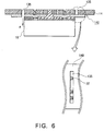
- the slits 135 may be formed in the carrier film with being extended radially from the corners of the chip mounting region as illustrated in Fig. 7.
- the illustrated slits each has a width of, for example 0.4 mm and has semicircular with a radius of 0.2 mm at both ends thereof.
- the position, dimension, and shape of the slits are not limited to the above mentioned illustrative embodiments.
- the slits may be formed in the carrier film at a plurality of positions. However, it is preferable that the slits are formed symmetrically relative to the chip mounting region to effectively reduce the warping of the carrier film.
Applications Claiming Priority (2)
| Application Number | Priority Date | Filing Date | Title |
|---|---|---|---|
| JP6237425A JP2586344B2 (ja) | 1994-09-30 | 1994-09-30 | キャリアフィルム |
| JP237425/94 | 1994-09-30 |
Publications (2)
| Publication Number | Publication Date |
|---|---|
| EP0704898A2 true EP0704898A2 (de) | 1996-04-03 |
| EP0704898A3 EP0704898A3 (de) | 1997-06-11 |
Family
ID=17015171
Family Applications (1)
| Application Number | Title | Priority Date | Filing Date |
|---|---|---|---|
| EP95306886A Withdrawn EP0704898A3 (de) | 1994-09-30 | 1995-09-29 | Trägerfilm |
Country Status (4)
| Country | Link |
|---|---|
| US (1) | US5757068A (de) |
| EP (1) | EP0704898A3 (de) |
| JP (1) | JP2586344B2 (de) |
| KR (1) | KR100268505B1 (de) |
Cited By (2)
| Publication number | Priority date | Publication date | Assignee | Title |
|---|---|---|---|---|
| DE19702014A1 (de) * | 1996-10-14 | 1998-04-16 | Fraunhofer Ges Forschung | Chipmodul sowie Verfahren zur Herstellung eines Chipmoduls |
| US6093971A (en) * | 1996-10-14 | 2000-07-25 | Fraunhofer-Gesellschaft Zur Forderung Der Angewandten Forschung E.V. | Chip module with conductor paths on the chip bonding side of a chip carrier |
Families Citing this family (15)
| Publication number | Priority date | Publication date | Assignee | Title |
|---|---|---|---|---|
| JP2843315B1 (ja) * | 1997-07-11 | 1999-01-06 | 株式会社日立製作所 | 半導体装置およびその製造方法 |
| US8071128B2 (en) * | 1996-06-14 | 2011-12-06 | Kyowa Hakko Kirin Co., Ltd. | Intrabuccally rapidly disintegrating tablet and a production method of the tablets |
| SG60099A1 (en) * | 1996-08-16 | 1999-02-22 | Sony Corp | Semiconductor package and manufacturing method of lead frame |
| US6077757A (en) * | 1997-05-15 | 2000-06-20 | Nec Corporation | Method of forming chip semiconductor devices |
| JP3555927B2 (ja) * | 1999-04-07 | 2004-08-18 | Necエレクトロニクス株式会社 | テープキャリアパッケージ |
| JP3360723B2 (ja) * | 1999-06-08 | 2002-12-24 | 日本電気株式会社 | 半導体素子のチップサイズパッケージ |
| US6239489B1 (en) * | 1999-07-30 | 2001-05-29 | Micron Technology, Inc. | Reinforcement of lead bonding in microelectronics packages |
| DE10010979A1 (de) * | 2000-03-07 | 2001-09-13 | Bosch Gmbh Robert | Elektrische Schaltung und Substrat hierzu |
| US6853178B2 (en) | 2000-06-19 | 2005-02-08 | Texas Instruments Incorporated | Integrated circuit leadframes patterned for measuring the accurate amplitude of changing currents |
| JP2002368156A (ja) * | 2001-06-11 | 2002-12-20 | Oki Electric Ind Co Ltd | 半導体装置及びその製造方法 |
| US7421411B2 (en) * | 2001-07-06 | 2008-09-02 | Nokia Corporation | Digital rights management in a mobile communications environment |
| JP5095460B2 (ja) * | 2008-01-17 | 2012-12-12 | シャープ株式会社 | 半導体装置および表示装置 |
| US11024595B2 (en) * | 2017-06-16 | 2021-06-01 | Micron Technology, Inc. | Thermocompression bond tips and related apparatus and methods |
| US11410964B2 (en) * | 2019-11-22 | 2022-08-09 | Micron Technology, Inc. | Contaminant control in thermocompression bonding of semiconductors and associated systems and methods |
| DE102022003764A1 (de) | 2022-10-12 | 2024-04-18 | Giesecke+Devrient ePayments GmbH | Modulträgerband |
Citations (3)
| Publication number | Priority date | Publication date | Assignee | Title |
|---|---|---|---|---|
| JPH04216660A (ja) | 1990-12-17 | 1992-08-06 | Dainippon Printing Co Ltd | 半導体素子用リードフレーム |
| JPH05129366A (ja) | 1991-11-08 | 1993-05-25 | Fujitsu Ltd | 集積回路用tab実装構造 |
| JPH0677293A (ja) | 1992-06-25 | 1994-03-18 | Nitto Denko Corp | フィルムキャリアおよびこれを用いた半導体装置 |
Family Cites Families (15)
| Publication number | Priority date | Publication date | Assignee | Title |
|---|---|---|---|---|
| JPS4952973A (de) * | 1972-09-22 | 1974-05-23 | ||
| JPS63237425A (ja) * | 1987-03-25 | 1988-10-03 | Toshiba Corp | 半導体装置 |
| US5028986A (en) * | 1987-12-28 | 1991-07-02 | Hitachi, Ltd. | Semiconductor device and semiconductor module with a plurality of stacked semiconductor devices |
| US5223741A (en) * | 1989-09-01 | 1993-06-29 | Tactical Fabs, Inc. | Package for an integrated circuit structure |
| JP2761779B2 (ja) * | 1989-12-13 | 1998-06-04 | トーワ株式会社 | フィルムキャリアとこれを用いるモールド方法 |
| KR940006185Y1 (ko) * | 1990-06-07 | 1994-09-10 | 가시오 게이상기 가부시끼가이샤 | Ic 모듈 |
| JPH0456143A (ja) * | 1990-06-22 | 1992-02-24 | Hitachi Ltd | 半導体装置および半導体装置の製造方法 |
| JPH04123448A (ja) * | 1990-09-14 | 1992-04-23 | Toshiba Corp | 半導体実装装置 |
| JPH05275498A (ja) * | 1991-03-20 | 1993-10-22 | Fujitsu Ltd | テープキャリアとそれを用いた半導体装置の組立方法 |
| JPH04329650A (ja) * | 1991-04-30 | 1992-11-18 | Nippon Steel Corp | Tabテープ |
| JPH04365343A (ja) * | 1991-06-13 | 1992-12-17 | Hitachi Cable Ltd | Tab用テープキャリア |
| JPH057868A (ja) * | 1991-07-03 | 1993-01-19 | Hitachi Ltd | 浄水器 |
| US5350947A (en) * | 1991-11-12 | 1994-09-27 | Nec Corporation | Film carrier semiconductor device |
| JPH05326648A (ja) * | 1992-05-22 | 1993-12-10 | Sony Corp | フィルムキャリアとこれを用いた半導体装置の製造方法 |
| US5586666A (en) * | 1995-06-12 | 1996-12-24 | Mechtronics Corporation | Foldable and expandable promotional pallet |
-
1994
- 1994-09-30 JP JP6237425A patent/JP2586344B2/ja not_active Expired - Fee Related
-
1995
- 1995-09-25 US US08/533,208 patent/US5757068A/en not_active Expired - Fee Related
- 1995-09-29 KR KR1019950033150A patent/KR100268505B1/ko not_active IP Right Cessation
- 1995-09-29 EP EP95306886A patent/EP0704898A3/de not_active Withdrawn
Patent Citations (3)
| Publication number | Priority date | Publication date | Assignee | Title |
|---|---|---|---|---|
| JPH04216660A (ja) | 1990-12-17 | 1992-08-06 | Dainippon Printing Co Ltd | 半導体素子用リードフレーム |
| JPH05129366A (ja) | 1991-11-08 | 1993-05-25 | Fujitsu Ltd | 集積回路用tab実装構造 |
| JPH0677293A (ja) | 1992-06-25 | 1994-03-18 | Nitto Denko Corp | フィルムキャリアおよびこれを用いた半導体装置 |
Cited By (2)
| Publication number | Priority date | Publication date | Assignee | Title |
|---|---|---|---|---|
| DE19702014A1 (de) * | 1996-10-14 | 1998-04-16 | Fraunhofer Ges Forschung | Chipmodul sowie Verfahren zur Herstellung eines Chipmoduls |
| US6093971A (en) * | 1996-10-14 | 2000-07-25 | Fraunhofer-Gesellschaft Zur Forderung Der Angewandten Forschung E.V. | Chip module with conductor paths on the chip bonding side of a chip carrier |
Also Published As
| Publication number | Publication date |
|---|---|
| KR100268505B1 (ko) | 2000-11-01 |
| EP0704898A3 (de) | 1997-06-11 |
| US5757068A (en) | 1998-05-26 |
| JPH08102475A (ja) | 1996-04-16 |
| JP2586344B2 (ja) | 1997-02-26 |
Similar Documents
| Publication | Publication Date | Title |
|---|---|---|
| EP0704895B1 (de) | Verfahren zur Herstellung einer halbleitenden Anordnung und einer Halbleiterscheibe | |
| KR100339044B1 (ko) | 볼그리드어레이 반도체패키지 및 그 제조방법 | |
| US5843808A (en) | Structure and method for automated assembly of a tab grid array package | |
| US6790710B2 (en) | Method of manufacturing an integrated circuit package | |
| US6060778A (en) | Ball grid array package | |
| US5661088A (en) | Electronic component and method of packaging | |
| US7638879B2 (en) | Semiconductor package and fabrication method thereof | |
| US6395582B1 (en) | Methods for forming ground vias in semiconductor packages | |
| US7816187B2 (en) | Method for fabricating semiconductor package free of substrate | |
| US5757068A (en) | Carrier film with peripheral slits | |
| US5567656A (en) | Process for packaging semiconductor device | |
| US6339253B1 (en) | Semiconductor package | |
| JP3759572B2 (ja) | 半導体装置 | |
| EP1035580A2 (de) | Verfahren und Struktur für integrierte Schaltung | |
| JP3529507B2 (ja) | 半導体装置 | |
| KR101008534B1 (ko) | 전력용 반도체모듈패키지 및 그 제조방법 | |
| JPH10154768A (ja) | 半導体装置及びその製造方法 | |
| KR100520443B1 (ko) | 칩스케일패키지및그제조방법 | |
| US20030214019A1 (en) | Packaging system for semiconductor devices | |
| KR100249539B1 (ko) | 반도체 칩 및 그 제조방법 | |
| US20060012035A1 (en) | Method of packaging integrated circuits, and integrated circuit packages produced by the method | |
| JPH08172142A (ja) | 半導体パッケージ及びその製造方法並びに半導体装置 | |
| KR100308393B1 (ko) | 반도체패키지및그제조방법 | |
| JPH07326690A (ja) | 半導体装置用パッケージおよび半導体装置 | |
| JPH11163253A (ja) | 半導体チップの実装構造、半導体装置および半導体装置の製造方法 |
Legal Events
| Date | Code | Title | Description |
|---|---|---|---|
| PUAI | Public reference made under article 153(3) epc to a published international application that has entered the european phase |
Free format text: ORIGINAL CODE: 0009012 |
|
| AK | Designated contracting states |
Kind code of ref document: A2 Designated state(s): DE FR GB |
|
| PUAL | Search report despatched |
Free format text: ORIGINAL CODE: 0009013 |
|
| AK | Designated contracting states |
Kind code of ref document: A3 Designated state(s): DE FR GB |
|
| 17P | Request for examination filed |
Effective date: 19970521 |
|
| 17Q | First examination report despatched |
Effective date: 19990317 |
|
| RAP1 | Party data changed (applicant data changed or rights of an application transferred) |
Owner name: NEC ELECTRONICS CORPORATION |
|
| STAA | Information on the status of an ep patent application or granted ep patent |
Free format text: STATUS: THE APPLICATION HAS BEEN WITHDRAWN |
|
| 18W | Application withdrawn |
Effective date: 20031024 |