EP0683531A2 - MOSFET mit LDD Struktur und Verfahren zur Herstellung - Google Patents
MOSFET mit LDD Struktur und Verfahren zur Herstellung Download PDFInfo
- Publication number
- EP0683531A2 EP0683531A2 EP95303269A EP95303269A EP0683531A2 EP 0683531 A2 EP0683531 A2 EP 0683531A2 EP 95303269 A EP95303269 A EP 95303269A EP 95303269 A EP95303269 A EP 95303269A EP 0683531 A2 EP0683531 A2 EP 0683531A2
- Authority
- EP
- European Patent Office
- Prior art keywords
- impurity
- conductivity type
- impurity region
- region
- gate electrode
- Prior art date
- Legal status (The legal status is an assumption and is not a legal conclusion. Google has not performed a legal analysis and makes no representation as to the accuracy of the status listed.)
- Granted
Links
- 238000004519 manufacturing process Methods 0.000 title claims abstract description 37
- 239000012535 impurity Substances 0.000 claims abstract description 361
- 239000000758 substrate Substances 0.000 claims abstract description 62
- 238000009413 insulation Methods 0.000 claims abstract description 50
- 239000004065 semiconductor Substances 0.000 claims abstract description 45
- 150000002500 ions Chemical class 0.000 claims description 33
- 125000006850 spacer group Chemical group 0.000 claims description 30
- 229920002120 photoresistant polymer Polymers 0.000 claims description 23
- 229910052698 phosphorus Inorganic materials 0.000 claims description 15
- 239000011574 phosphorus Substances 0.000 claims description 15
- 229910052785 arsenic Inorganic materials 0.000 claims description 14
- OAICVXFJPJFONN-UHFFFAOYSA-N Phosphorus Chemical compound [P] OAICVXFJPJFONN-UHFFFAOYSA-N 0.000 claims description 13
- RQNWIZPPADIBDY-UHFFFAOYSA-N arsenic atom Chemical compound [As] RQNWIZPPADIBDY-UHFFFAOYSA-N 0.000 claims description 12
- 230000000873 masking effect Effects 0.000 claims description 3
- 229910044991 metal oxide Inorganic materials 0.000 claims description 3
- 150000004706 metal oxides Chemical class 0.000 claims description 3
- 238000000034 method Methods 0.000 abstract description 20
- 230000005684 electric field Effects 0.000 abstract description 5
- 230000010354 integration Effects 0.000 abstract description 4
- 230000015556 catabolic process Effects 0.000 description 15
- 238000005468 ion implantation Methods 0.000 description 8
- -1 e.g. Chemical class 0.000 description 7
- 238000007796 conventional method Methods 0.000 description 5
- 238000005530 etching Methods 0.000 description 5
- 229910021420 polycrystalline silicon Inorganic materials 0.000 description 5
- 229920005591 polysilicon Polymers 0.000 description 4
- 230000000694 effects Effects 0.000 description 3
- 239000011810 insulating material Substances 0.000 description 3
- 230000001590 oxidative effect Effects 0.000 description 3
- 238000006731 degradation reaction Methods 0.000 description 2
- 239000012774 insulation material Substances 0.000 description 2
- 238000002955 isolation Methods 0.000 description 2
- 238000007669 thermal treatment Methods 0.000 description 2
- 239000004020 conductor Substances 0.000 description 1
- 238000000151 deposition Methods 0.000 description 1
- 238000009792 diffusion process Methods 0.000 description 1
- 230000003647 oxidation Effects 0.000 description 1
- 238000007254 oxidation reaction Methods 0.000 description 1
- 238000002161 passivation Methods 0.000 description 1
Images

Classifications
-
- H—ELECTRICITY
- H01—ELECTRIC ELEMENTS
- H01L—SEMICONDUCTOR DEVICES NOT COVERED BY CLASS H10
- H01L29/00—Semiconductor devices specially adapted for rectifying, amplifying, oscillating or switching and having potential barriers; Capacitors or resistors having potential barriers, e.g. a PN-junction depletion layer or carrier concentration layer; Details of semiconductor bodies or of electrodes thereof ; Multistep manufacturing processes therefor
- H01L29/66—Types of semiconductor device ; Multistep manufacturing processes therefor
- H01L29/66007—Multistep manufacturing processes
- H01L29/66075—Multistep manufacturing processes of devices having semiconductor bodies comprising group 14 or group 13/15 materials
- H01L29/66227—Multistep manufacturing processes of devices having semiconductor bodies comprising group 14 or group 13/15 materials the devices being controllable only by the electric current supplied or the electric potential applied, to an electrode which does not carry the current to be rectified, amplified or switched, e.g. three-terminal devices
- H01L29/66409—Unipolar field-effect transistors
- H01L29/66477—Unipolar field-effect transistors with an insulated gate, i.e. MISFET
- H01L29/66568—Lateral single gate silicon transistors
- H01L29/66575—Lateral single gate silicon transistors where the source and drain or source and drain extensions are self-aligned to the sides of the gate
- H01L29/6659—Lateral single gate silicon transistors where the source and drain or source and drain extensions are self-aligned to the sides of the gate with both lightly doped source and drain extensions and source and drain self-aligned to the sides of the gate, e.g. lightly doped drain [LDD] MOSFET, double diffused drain [DDD] MOSFET
-
- H—ELECTRICITY
- H01—ELECTRIC ELEMENTS
- H01L—SEMICONDUCTOR DEVICES NOT COVERED BY CLASS H10
- H01L29/00—Semiconductor devices specially adapted for rectifying, amplifying, oscillating or switching and having potential barriers; Capacitors or resistors having potential barriers, e.g. a PN-junction depletion layer or carrier concentration layer; Details of semiconductor bodies or of electrodes thereof ; Multistep manufacturing processes therefor
- H01L29/66—Types of semiconductor device ; Multistep manufacturing processes therefor
- H01L29/68—Types of semiconductor device ; Multistep manufacturing processes therefor controllable by only the electric current supplied, or only the electric potential applied, to an electrode which does not carry the current to be rectified, amplified or switched
- H01L29/76—Unipolar devices, e.g. field effect transistors
- H01L29/772—Field effect transistors
- H01L29/78—Field effect transistors with field effect produced by an insulated gate
-
- H—ELECTRICITY
- H01—ELECTRIC ELEMENTS
- H01L—SEMICONDUCTOR DEVICES NOT COVERED BY CLASS H10
- H01L29/00—Semiconductor devices specially adapted for rectifying, amplifying, oscillating or switching and having potential barriers; Capacitors or resistors having potential barriers, e.g. a PN-junction depletion layer or carrier concentration layer; Details of semiconductor bodies or of electrodes thereof ; Multistep manufacturing processes therefor
- H01L29/66—Types of semiconductor device ; Multistep manufacturing processes therefor
- H01L29/66007—Multistep manufacturing processes
- H01L29/66075—Multistep manufacturing processes of devices having semiconductor bodies comprising group 14 or group 13/15 materials
- H01L29/66227—Multistep manufacturing processes of devices having semiconductor bodies comprising group 14 or group 13/15 materials the devices being controllable only by the electric current supplied or the electric potential applied, to an electrode which does not carry the current to be rectified, amplified or switched, e.g. three-terminal devices
- H01L29/66409—Unipolar field-effect transistors
- H01L29/66477—Unipolar field-effect transistors with an insulated gate, i.e. MISFET
- H01L29/66568—Lateral single gate silicon transistors
- H01L29/66659—Lateral single gate silicon transistors with asymmetry in the channel direction, e.g. lateral high-voltage MISFETs with drain offset region, extended drain MISFETs
-
- H—ELECTRICITY
- H01—ELECTRIC ELEMENTS
- H01L—SEMICONDUCTOR DEVICES NOT COVERED BY CLASS H10
- H01L29/00—Semiconductor devices specially adapted for rectifying, amplifying, oscillating or switching and having potential barriers; Capacitors or resistors having potential barriers, e.g. a PN-junction depletion layer or carrier concentration layer; Details of semiconductor bodies or of electrodes thereof ; Multistep manufacturing processes therefor
- H01L29/66—Types of semiconductor device ; Multistep manufacturing processes therefor
- H01L29/68—Types of semiconductor device ; Multistep manufacturing processes therefor controllable by only the electric current supplied, or only the electric potential applied, to an electrode which does not carry the current to be rectified, amplified or switched
- H01L29/76—Unipolar devices, e.g. field effect transistors
- H01L29/772—Field effect transistors
- H01L29/78—Field effect transistors with field effect produced by an insulated gate
- H01L29/7833—Field effect transistors with field effect produced by an insulated gate with lightly doped drain or source extension, e.g. LDD MOSFET's; DDD MOSFET's
- H01L29/7835—Field effect transistors with field effect produced by an insulated gate with lightly doped drain or source extension, e.g. LDD MOSFET's; DDD MOSFET's with asymmetrical source and drain regions, e.g. lateral high-voltage MISFETs with drain offset region, extended drain MISFETs
-
- H—ELECTRICITY
- H01—ELECTRIC ELEMENTS
- H01L—SEMICONDUCTOR DEVICES NOT COVERED BY CLASS H10
- H01L29/00—Semiconductor devices specially adapted for rectifying, amplifying, oscillating or switching and having potential barriers; Capacitors or resistors having potential barriers, e.g. a PN-junction depletion layer or carrier concentration layer; Details of semiconductor bodies or of electrodes thereof ; Multistep manufacturing processes therefor
- H01L29/66—Types of semiconductor device ; Multistep manufacturing processes therefor
- H01L29/68—Types of semiconductor device ; Multistep manufacturing processes therefor controllable by only the electric current supplied, or only the electric potential applied, to an electrode which does not carry the current to be rectified, amplified or switched
- H01L29/76—Unipolar devices, e.g. field effect transistors
- H01L29/772—Field effect transistors
- H01L29/78—Field effect transistors with field effect produced by an insulated gate
- H01L29/7833—Field effect transistors with field effect produced by an insulated gate with lightly doped drain or source extension, e.g. LDD MOSFET's; DDD MOSFET's
- H01L29/7836—Field effect transistors with field effect produced by an insulated gate with lightly doped drain or source extension, e.g. LDD MOSFET's; DDD MOSFET's with a significant overlap between the lightly doped extension and the gate electrode
-
- Y—GENERAL TAGGING OF NEW TECHNOLOGICAL DEVELOPMENTS; GENERAL TAGGING OF CROSS-SECTIONAL TECHNOLOGIES SPANNING OVER SEVERAL SECTIONS OF THE IPC; TECHNICAL SUBJECTS COVERED BY FORMER USPC CROSS-REFERENCE ART COLLECTIONS [XRACs] AND DIGESTS
- Y10—TECHNICAL SUBJECTS COVERED BY FORMER USPC
- Y10S—TECHNICAL SUBJECTS COVERED BY FORMER USPC CROSS-REFERENCE ART COLLECTIONS [XRACs] AND DIGESTS
- Y10S257/00—Active solid-state devices, e.g. transistors, solid-state diodes
- Y10S257/90—MOSFET type gate sidewall insulating spacer
-
- Y—GENERAL TAGGING OF NEW TECHNOLOGICAL DEVELOPMENTS; GENERAL TAGGING OF CROSS-SECTIONAL TECHNOLOGIES SPANNING OVER SEVERAL SECTIONS OF THE IPC; TECHNICAL SUBJECTS COVERED BY FORMER USPC CROSS-REFERENCE ART COLLECTIONS [XRACs] AND DIGESTS
- Y10—TECHNICAL SUBJECTS COVERED BY FORMER USPC
- Y10S—TECHNICAL SUBJECTS COVERED BY FORMER USPC CROSS-REFERENCE ART COLLECTIONS [XRACs] AND DIGESTS
- Y10S438/00—Semiconductor device manufacturing: process
- Y10S438/942—Masking
- Y10S438/948—Radiation resist
Definitions
- the present invention relates to a metal-oxide semiconductor (MOS) transistor, and more particularly, to a high-voltage transistor in which layout space can be reduced and for which improved characteristics can be provided, and a manufacturing method for such a transistor.
- MOS metal-oxide semiconductor
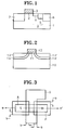
- FIG. 1 of the accompanying drawings is a cross-sectional view of a transistor having a high breakdown voltage, which is disclosed in U.S. Patent No. 4,172,260.
- a first oxide film (not shown) is formed on a P-type semiconductor substrate 1 by a thermal oxidation. After selectively etching the first oxide film, an N+-type impurity is diffused into the substrate 1 to form an N+-type source region 7 and drain region 6. The first oxide film is removed and a thermal oxidizing process is conducted to form a second oxide film 2 on the substrate 1. After depositing a polycrystalline silicon (polysilicon) on the second oxide film 2, the polysilicon layer is patterned by a photolithographic etching process to form a gate electrode 3. Then, using gate electrode 3 as a mask, N ⁇ -type impurity ions are implanted to form an N ⁇ -type register region 8.
- a third oxide film (not shown) which extends from on the gate electrode 3 toward the drain region 6 and which terminates at an intermediate position of the resistor region 8 is formed.
- N-type impurity ions are implanted to form an N-type intermediate region 5.
- the register region 8 is segmented into N ⁇ -type region 4 and N-type intermediate region 5.
- a passivation film (not shown) is formed on the resultant structure, and a contact process for exposing the source region 7 and drain region 6 is conducted.
- the width of a depletion layer formed near the drain region is made large by forming N ⁇ - and N-type regions between the N+-drain region of a transistor and gate electrode 3, the electrical field applied to the drain region is reduced.
- the layout space is increased by as much as the offset length corresponding to the N ⁇ - and N-type regions, which is disadvantageous for high-integration.
- a gate insulation film 11 is formed on a P-type semiconductor substrate 10 by a thermal oxidizing process. Subsequently, polysilicon is deposited thereon and patterned by a photolithographic etching process to form a gate electrode 12. Using the gate electrode 12 as a mask, N ⁇ -type impurity ions are implanted. Next, N ⁇ source and drain regions 14 and 14' in which a deep junction is diffused are formed by conducting a thermal treatment at a high temperature for a long time. Using the gate electrode 12 again as a mask, N+-impurity ions are again implanted, thereby forming N+ source and drain regions 13 and 13'.
- a transistor comprising: a semiconductor substrate of a first conductivity type; a gate electrode formed by interposing a gate insulation film on the semiconductor substrate; an insulation spacer formed on the sidewalls of the gate electrode; a first impurity region of a first conductivity type formed on the substrate surface under the gate electrode and having a first impurity concentration; a pair of second impurity regions of a second conductivity type, being opposite to the first conductivity type, formed on the left and right of the first impurity region, respectively, and having a second impurity concentration; a pair of third impurity regions formed between the first and second impurity regions, having a smaller junction depth than that of the second impurity region and a third impurity concentration lower than that of the second impurity region; and a pair of fourth impurity regions aligned with the insulation spacer, respectively embedded in and having a higher concentration than the pair of second impurity regions.
- the third impurity region has a width which extends 0.2 ⁇ 1.0 ⁇ m from the edge of the gate electrode toward the center thereof.
- the insulation spacer is formed so as to cover the upper surface of each second impurity region not being contacted with each fourth impurity region.
- the first conductivity type is an N-type and the second conductivity type is a P-type, or vice versa.
- phosphorus may be used as the impurity of the second and third impurity regions and arsenic may be used as that of the fourth impurity region.
- a MOS transistor comprising: a semiconductor substrate of a first conductivity type; a gate electrode formed by interposing a gate insulation film on the semiconductor substrate; an insulation spacer formed on the sidewalls of the gate electrode; a first impurity region of the first conductivity type formed on the substrate surface under the gate electrode and having a first impurity concentration; a second impurity region of a second conductivity type, being opposite to the first conductivity type, contacting one side of the first impurity region and having a second impurity concentration being higher than the first impurity concentration; a third impurity region of the second conductivity type formed on the other side of the first impurity region and having a third impurity concentration being higher than the second impurity concentration; a fourth impurity region of the second conductivity type formed between the first impurity region and third impurity region, with contacting the other side of the first impurity region, and having a fourth impurity concentration being lower than the second im
- the fourth impurity region has a width of 0.2 ⁇ 1.0 ⁇ m which extends from the edge of the gate electrode toward the center thereof, and the insulation spacer is formed so as to cover the upper surface of the second impurity region with which the sixth impurity region is not contacted and the upper surface of the third impurity region with which the seventh impurity region is not contacted.
- Phosphorus may be used as the impurity of the second to fifth impurity regions and arsenic is used as the impurity of the sixth and seventh impurity regions.
- phosphorus may be used as the impurity of the fourth and fifth impurity regions and arsenic may be used as the impurity of the second, third, sixth and seventh impurity regions.
- a method of manufacturing a transistor which comprises the steps of: implanting first impurity ions of a first conductivity type on a semiconductor substrate of the first conductivity type, to form a first impurity region of a first impurity concentration thereon; sequentially forming a gate insulation film and a gate electrode on the semiconductor substrate; forming a photoresist pattern on the gate electrode, each side of the photoresist pattern being at a first predetermined distance from the edges of the gate electrode toward the center thereof for masking the gate electrode; implanting second impurity ions of a second conductivity type, being opposite to the first conductivity type, on the resultant structure on which the photoresist pattern is formed, to form a pair of second impurity regions having a second impurity concentration into the semiconductor substrate, and at the same time forming a pair of third impurity regions contacting the pair of second impurity regions, having a width which extends from both edges of the gate electrode toward the center thereof by the predetermined
- the third impurity concentration of the third impurity regions is preferably higher than the first impurity concentration of the first impurity region.
- the first predetermined distance is preferably 0.2 ⁇ 1.0 ⁇ m.
- Phosphorus is preferably used as the second impurity and arsenic is preferably used as the third impurity.
- a method of manufacturing a transistor which comprises the steps of: implanting first impurity ions of a first conductivity type on a semiconductor substrate of the first conductivity type, to form a first impurity region of a first impurity concentration thereon; sequentially forming a gate insulation film and a gate electrode on the semiconductor substrate; implanting second impurity ions of a second conductivity type, being opposite to the first conductivity type, on the resultant structure on which said gate insulation film and gate electrode are formed, to form second and third impurity regions in the semiconductor substrate, each having a second impurity concentration and a third impurity concentration being higher than the second impurity concentration; forming a photoresist pattern to cover the part of the gate electrode and the substrate where the second impurity region is formed and to expose the other part of the gate electrode and the substrate where the third impurity region is formed; implanting third impurity ions of the second conductivity type on the resultant structure on which the photoresist pattern is
- the third impurity concentration of the fourth impurity region is preferably higher than the first impurity concentration of the first impurity region.
- Phosphorus is preferably used as the second and third impurities and arsenic is preferably used as the fourth impurity.
- phosphorus is preferably used as the third impurity and arsenic is preferably used as the second and fourth impurities.
- reference letter A designates an active region pattern
- G designates a gate pattern
- S designates a source region
- D designates a drain region
- P designates a source/drain ion implantation pattern.
- the source/drain pattern P according to the present invention is formed on the gate pattern G and both patterns P and G are overlapped by a distance b .
- FIGs. 4 and 5 are cross-sectional views along a line aa' of FIG. 3 for explaining a method for manufacturing the high- voltage transistor according to an embodiment of the present invention.
- FIG. 4 shows a process of forming N ⁇ -type source/drain 56 and 56' and N ⁇ -type source/drain 53.
- a device isolation region (not shown) for defining an active region on a P-type semiconductor substrate 50 is selectively formed.
- an impurity region 51 for controlling a threshold voltage is formed on the surface of the substrate 50 of the active region.
- an insulating material is formed on the substrate 50 by a thermal oxidizing process and a conductive material, e.g., polysilicon, is successively deposited on the insulating material to form a conductive layer.
- the conductive layer and the insulating material are patterned by a photolithographic etching process to form a gate electrode 54 and a gate insulation film 52.
- a photoresist pattern PR is formed on the resultant structure so as to mask the gate electrode 54, each side of the photoresist pattern being at a first predetermined distance b , e.g., 0.2 ⁇ 1.0 ⁇ m, from the edges of the gate electrode 54 toward the center of the gate electrode 54.
- N ⁇ -type impurity ions e.g., phosphorus ions
- N ⁇ source and drain regions 56 and 56' and N ⁇ source/drain region 53 are formed on the substrate 50 at the same time.
- the N ⁇ source/drain region 53 is a tail portion of impurity profile produced b y a high energy ion implantation and has a width extending from both edges of the gate electrode 54 toward the center thereof by a first predetermined distance b , and is formed in the substrate under the gate electrode 54. Also, the impurity concentration of the N ⁇ source/drain region 53 is lower than that of N ⁇ source and drain regions 56 and 56' and is higher than that of impurity region 51.
- FIG. 5 shows a process of forming N+ source/drain 60 and 60'.
- an insulation material is deposited on the whole surface of the resultant structure.
- an insulation spacer 58 is formed on the sidewalls of the gate electrode 54 by anisotropic-etching the insulation material.
- N+-type impurity ions e.g., arsenic ions
- the gate electrode 54 and insulation spacer 58 are formed on the substrate 50.
- the N+ source and drain regions 60 and 60' are formed so as to be respectively included in the N ⁇ source and drain regions 56 and 56'.
- the insulation spacer 58 is formed so as to cover the predetermined surface of the N ⁇ source region 56 not being contacted with the N+ source region 60 and the predetermined surface of the N ⁇ drain region 56' not being contacted with the N+ drain region 60'.
- the N ⁇ source/drain region is formed on the substrate surface under gate electrode 54 and has a width ranging from the edge portion of the gate electrode to the center thereof by a first distance, a deep depletion of the source/drain junction portion is reduced. Also, since the width of the depletion is increased, the electric field applied to the drain region is reduced. Also, since the N ⁇ source/drain region is controlled by a gate voltage to decrease a degradation of transistor characteristics due to a carrier trap, a high reliability on a hot carrier can be achieved. Also, since the N ⁇ source and drain regions having deep junction portion are formed by a high energy ion implantation, an additional diffusion process is not required after conducting the N ⁇ source/drain ion implantation. Therefore, the performance degradation of other transistor types, e.g., low-voltage transistors, can be prevented.
- FIG. 6 is a plan view of a high-voltage transistor according to another embodiment of the present invention and reference letters indicated therein are the same as those in FIG. 3.
- N ⁇ source/drain ion implantation pattern P is formed only on the drain region D to which a high voltage is applied.
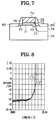
- FIG. 7 is a cross-sectional view along a line cc' of FIG. 6 for explaining a method for manufacturing the high-voltage transistor according to another embodiment of the present invention.
- N ⁇ -type impurity ions e.g., phosphorus or arsenic ions
- a photoresist pattern is formed on the resultant structure so as to cover the N ⁇ -region (77) and one part of the gate electrode (74) and to expose N ⁇ -region (77') and the other part of the gate electrode 74 wherein the width of the exposed gate electrode corresponds to a predetermined distance b , e.g., 0.2 ⁇ 1.0 ⁇ m, from one edge of the gate electrode 74 near the N ⁇ drain region 77' toward the center thereof.
- N ⁇ -type impurity ions e.g., phosphorus ions
- the N ⁇ region 73 formed in the surface of substrate 70 under the gate electrode 74, is a tail portion of impurity profile produced by a high energy ion implantation and extends from the edge of the gate electrode 74 of the N ⁇ drain region to the center thereof by a first distance.
- the concentration of the N ⁇ region 76 is the same as that of N ⁇ source region 77 and is lower than that of the N ⁇ drain region 77'.
- the concentration of the N ⁇ region 73 is lower than that of the N ⁇ region 76 and is higher than that of the P ⁇ -type impurity region 71.
- an insulation spacer 78 and N+-type source and drain regions 80 and 80' are formed by the method described in connection with FIG. 5.
- the impurity concentration is the same for the N+-type source and drain regions 80 and 80' which is higher than that of the N ⁇ drain region 77'.
- the N ⁇ source/drain ion implantation is conducted only with respect to the drain region to which a high voltage is applied like in the N ⁇ source/drain ion implantation for a high-voltage transistor.
- the layout space is greatly reduced with respect to the first embodiment, the integration of semiconductors is considerably increased.
- FIG. 8 is a graph showing breakdown voltage characteristics of the high-voltage transistors manufactured by the conventional method and the present invention.
- the transistor according to the present invention has an increased breakdown voltage with respect to that by the conventional method.
- the width of the depletion layer of the source/drain junction portion is increased due to the N ⁇ source and drain regions 53 and 73 extending from the edge portion of the gate electrode toward the center thereof by a first predetermined distance and formed on the surface of the substrate under the gate electrode, the electric field applied to the drain region can be reduced. Also, since the N ⁇ region is formed only on the drain region to which a high voltage is applied, the layout space can become smaller. Therefore, the integration of semiconductor devices can be increased.
Landscapes
- Engineering & Computer Science (AREA)
- Microelectronics & Electronic Packaging (AREA)
- Power Engineering (AREA)
- Physics & Mathematics (AREA)
- Ceramic Engineering (AREA)
- Condensed Matter Physics & Semiconductors (AREA)
- General Physics & Mathematics (AREA)
- Computer Hardware Design (AREA)
- Manufacturing & Machinery (AREA)
- Insulated Gate Type Field-Effect Transistor (AREA)
- Metal-Oxide And Bipolar Metal-Oxide Semiconductor Integrated Circuits (AREA)
Applications Claiming Priority (2)
| Application Number | Priority Date | Filing Date | Title |
|---|---|---|---|
| KR1019940010668A KR100189964B1 (ko) | 1994-05-16 | 1994-05-16 | 고전압 트랜지스터 및 그 제조방법 |
| KR9410668 | 1994-05-16 |
Publications (3)
| Publication Number | Publication Date |
|---|---|
| EP0683531A2 true EP0683531A2 (de) | 1995-11-22 |
| EP0683531A3 EP0683531A3 (de) | 1996-02-28 |
| EP0683531B1 EP0683531B1 (de) | 1999-03-17 |
Family
ID=19383164
Family Applications (1)
| Application Number | Title | Priority Date | Filing Date |
|---|---|---|---|
| EP95303269A Expired - Lifetime EP0683531B1 (de) | 1994-05-16 | 1995-05-16 | MOSFET mit LDD Struktur und Verfahren zur Herstellung |
Country Status (5)
| Country | Link |
|---|---|
| US (2) | US5567965A (de) |
| EP (1) | EP0683531B1 (de) |
| JP (1) | JP4009331B2 (de) |
| KR (1) | KR100189964B1 (de) |
| DE (1) | DE69508302T2 (de) |
Cited By (2)
| Publication number | Priority date | Publication date | Assignee | Title |
|---|---|---|---|---|
| WO2010035143A3 (ko) * | 2008-09-29 | 2010-10-14 | 크로스텍 캐피탈 엘엘씨 | 트랜지스터, 이를 구비한 이미지 센서 및 그의 제조방법 |
| CN102446763A (zh) * | 2010-10-13 | 2012-05-09 | 中芯国际集成电路制造(上海)有限公司 | Mos晶体管及其制作方法 |
Families Citing this family (11)
| Publication number | Priority date | Publication date | Assignee | Title |
|---|---|---|---|---|
| US5770880A (en) * | 1996-09-03 | 1998-06-23 | Harris Corporation | P-collector H.V. PMOS switch VT adjusted source/drain |
| KR100205320B1 (ko) * | 1996-10-25 | 1999-07-01 | 구본준 | 모스펫 및 그 제조방법 |
| US5793090A (en) * | 1997-01-10 | 1998-08-11 | Advanced Micro Devices, Inc. | Integrated circuit having multiple LDD and/or source/drain implant steps to enhance circuit performance |
| US6670103B2 (en) * | 2000-11-17 | 2003-12-30 | Macronix International Co., Ltd. | Method for forming lightly doped diffusion regions |
| JP4408679B2 (ja) * | 2003-10-09 | 2010-02-03 | 三洋電機株式会社 | 半導体装置の製造方法 |
| US7196375B2 (en) * | 2004-03-16 | 2007-03-27 | Taiwan Semiconductor Manufacturing Company, Ltd. | High-voltage MOS transistor |
| US7525150B2 (en) * | 2004-04-07 | 2009-04-28 | Taiwan Semiconductor Manufacturing Company, Ltd. | High voltage double diffused drain MOS transistor with medium operation voltage |
| KR100669858B1 (ko) * | 2005-05-13 | 2007-01-16 | 삼성전자주식회사 | 고전압 반도체 장치 및 그 제조 방법 |
| US8253198B2 (en) | 2009-07-30 | 2012-08-28 | Micron Technology | Devices for shielding a signal line over an active region |
| JP2011210901A (ja) * | 2010-03-29 | 2011-10-20 | Seiko Instruments Inc | デプレッション型mosトランジスタ |
| CN110660852A (zh) * | 2018-06-29 | 2020-01-07 | 立锜科技股份有限公司 | 金属氧化物半导体元件及其制造方法 |
Citations (2)
| Publication number | Priority date | Publication date | Assignee | Title |
|---|---|---|---|---|
| US4172260A (en) | 1976-12-01 | 1979-10-23 | Hitachi, Ltd. | Insulated gate field effect transistor with source field shield extending over multiple region channel |
| US4950617A (en) | 1986-11-07 | 1990-08-21 | Kabushiki Kaisha Toshiba | Method of manufacturing semiconductor device |
Family Cites Families (27)
| Publication number | Priority date | Publication date | Assignee | Title |
|---|---|---|---|---|
| JPS5645076A (en) * | 1979-09-21 | 1981-04-24 | Hitachi Ltd | Manufacturing of power mis field effect semiconductor device |
| JPS60133756A (ja) * | 1983-12-21 | 1985-07-16 | Seiko Epson Corp | 薄膜トランジスタの製造方法 |
| JPS60136376A (ja) * | 1983-12-26 | 1985-07-19 | Hitachi Ltd | 半導体装置の製造方法 |
| JPS60177677A (ja) * | 1984-02-23 | 1985-09-11 | Seiko Epson Corp | 半導体装置 |
| JPS61214473A (ja) * | 1985-03-19 | 1986-09-24 | Sony Corp | 電界効果型トランジスタ |
| GB2190790B (en) * | 1986-05-12 | 1989-12-13 | Plessey Co Plc | Improvements in transistors |
| US4682404A (en) * | 1986-10-23 | 1987-07-28 | Ncr Corporation | MOSFET process using implantation through silicon |
| US4746624A (en) * | 1986-10-31 | 1988-05-24 | Hewlett-Packard Company | Method for making an LDD MOSFET with a shifted buried layer and a blocking region |
| US4728617A (en) * | 1986-11-04 | 1988-03-01 | Intel Corporation | Method of fabricating a MOSFET with graded source and drain regions |
| US4818715A (en) * | 1987-07-09 | 1989-04-04 | Industrial Technology Research Institute | Method of fabricating a LDDFET with self-aligned silicide |
| JPS6484667A (en) * | 1987-09-28 | 1989-03-29 | Toshiba Corp | Insulated-gate transistor |
| US4878100A (en) * | 1988-01-19 | 1989-10-31 | Texas Instruments Incorporated | Triple-implanted drain in transistor made by oxide sidewall-spacer method |
| JPH01278074A (ja) * | 1988-04-28 | 1989-11-08 | Mitsubishi Electric Corp | Mis型トランジスタおよびその製造方法 |
| US5097300A (en) * | 1989-03-28 | 1992-03-17 | Seiko Epson Corporation | Semiconductor device and manufacturing method thereof |
| JPH0316123A (ja) * | 1989-03-29 | 1991-01-24 | Mitsubishi Electric Corp | イオン注入方法およびそれにより製造される半導体装置 |
| JP2781918B2 (ja) * | 1989-04-20 | 1998-07-30 | 三菱電機株式会社 | Mos型半導体装置の製造方法 |
| JP2789109B2 (ja) * | 1989-05-25 | 1998-08-20 | 三菱電機株式会社 | 半導体装置およびその製造方法 |
| JP2805646B2 (ja) * | 1989-09-20 | 1998-09-30 | ソニー株式会社 | 半導体装置の製造方法 |
| FR2654258A1 (fr) * | 1989-11-03 | 1991-05-10 | Philips Nv | Procede pour fabriquer un dispositif a transistor mis ayant une electrode de grille en forme de "t" inverse. |
| US5550069A (en) * | 1990-06-23 | 1996-08-27 | El Mos Electronik In Mos Technologie Gmbh | Method for producing a PMOS transistor |
| US5120668A (en) * | 1991-07-10 | 1992-06-09 | Ibm Corporation | Method of forming an inverse T-gate FET transistor |
| JPH05267327A (ja) * | 1992-03-18 | 1993-10-15 | Fujitsu Ltd | Misfet及びその製造方法 |
| US5292676A (en) * | 1992-07-29 | 1994-03-08 | Micron Semiconductor, Inc. | Self-aligned low resistance buried contact process |
| KR940022907A (ko) * | 1993-03-31 | 1994-10-21 | 이헌조 | 비대칭 엘디디(ldd) 접합 박막트랜지스터 |
| JP3221766B2 (ja) * | 1993-04-23 | 2001-10-22 | 三菱電機株式会社 | 電界効果トランジスタの製造方法 |
| KR0130376B1 (ko) * | 1994-02-01 | 1998-04-06 | 문정환 | 반도체소자 제조방법 |
| US5604139A (en) * | 1994-02-10 | 1997-02-18 | Semiconductor Energy Laboratory Co., Ltd. | Method for manufacturing a semiconductor device |
-
1994
- 1994-05-16 KR KR1019940010668A patent/KR100189964B1/ko not_active IP Right Cessation
-
1995
- 1995-05-15 JP JP11602495A patent/JP4009331B2/ja not_active Expired - Lifetime
- 1995-05-16 EP EP95303269A patent/EP0683531B1/de not_active Expired - Lifetime
- 1995-05-16 US US08/441,838 patent/US5567965A/en not_active Expired - Lifetime
- 1995-05-16 DE DE69508302T patent/DE69508302T2/de not_active Expired - Lifetime
-
1996
- 1996-03-08 US US08/613,240 patent/US5879995A/en not_active Expired - Lifetime
Patent Citations (2)
| Publication number | Priority date | Publication date | Assignee | Title |
|---|---|---|---|---|
| US4172260A (en) | 1976-12-01 | 1979-10-23 | Hitachi, Ltd. | Insulated gate field effect transistor with source field shield extending over multiple region channel |
| US4950617A (en) | 1986-11-07 | 1990-08-21 | Kabushiki Kaisha Toshiba | Method of manufacturing semiconductor device |
Cited By (3)
| Publication number | Priority date | Publication date | Assignee | Title |
|---|---|---|---|---|
| WO2010035143A3 (ko) * | 2008-09-29 | 2010-10-14 | 크로스텍 캐피탈 엘엘씨 | 트랜지스터, 이를 구비한 이미지 센서 및 그의 제조방법 |
| US8829577B2 (en) | 2008-09-29 | 2014-09-09 | Intellectual Ventures Ii Llc | Transistor, image sensor with the same, and method of manufacturing the same |
| CN102446763A (zh) * | 2010-10-13 | 2012-05-09 | 中芯国际集成电路制造(上海)有限公司 | Mos晶体管及其制作方法 |
Also Published As
| Publication number | Publication date |
|---|---|
| DE69508302D1 (de) | 1999-04-22 |
| US5567965A (en) | 1996-10-22 |
| KR950034822A (ko) | 1995-12-28 |
| EP0683531A3 (de) | 1996-02-28 |
| US5879995A (en) | 1999-03-09 |
| EP0683531B1 (de) | 1999-03-17 |
| JP4009331B2 (ja) | 2007-11-14 |
| JPH0846196A (ja) | 1996-02-16 |
| KR100189964B1 (ko) | 1999-06-01 |
| DE69508302T2 (de) | 1999-11-04 |
Similar Documents
| Publication | Publication Date | Title |
|---|---|---|
| US6277675B1 (en) | Method of fabricating high voltage MOS device | |
| US6518138B2 (en) | Method of forming Self-aligned lateral DMOS with spacer drift region | |
| US5930642A (en) | Transistor with buried insulative layer beneath the channel region | |
| JP2008514007A (ja) | スタック状ヘテロドーピング周縁部及び徐々に変化するドリフト領域を備えた促進された表面電界低減化高耐圧p型mosデバイス | |
| JPH06310717A (ja) | 電界効果トランジスタ及びその製造方法 | |
| JP3655467B2 (ja) | 二重拡散形mosトランジスタ及びその製造方法 | |
| EP0683531B1 (de) | MOSFET mit LDD Struktur und Verfahren zur Herstellung | |
| US7294551B2 (en) | Semiconductor device and method for manufacturing the same | |
| US6077736A (en) | Method of fabricating a semiconductor device | |
| JPH11111972A (ja) | 半導体デバイス及びその製造方法 | |
| KR19990050418A (ko) | 이중 필드판 구조를 갖는 전력소자 | |
| US6713331B2 (en) | Semiconductor device manufacturing using one element separation film | |
| KR950008257B1 (ko) | 모스(mos) 트랜지스터 및 그 제조방법 | |
| US6350641B1 (en) | Method of increasing the depth of lightly doping in a high voltage device | |
| JPH11220128A (ja) | Mosfet及びその製造方法 | |
| JPH03198349A (ja) | Mos型半導体装置の製造方法 | |
| EP0272755B1 (de) | Verfahren zur Herstellung eines Halbleiterbauelements | |
| KR19980053138A (ko) | 마스크 롬 코딩방법 | |
| JP2003115585A (ja) | 半導体装置の製造方法 | |
| KR0146276B1 (ko) | 모스펫 제조방법 | |
| JP4857493B2 (ja) | 半導体装置の製造方法 | |
| KR0125296B1 (ko) | 모스펫(mosfet) 제조방법 | |
| KR100587379B1 (ko) | 반도체 소자의 제조방법 | |
| KR100280798B1 (ko) | 반도체 소자의 트랜지스터 제조방법 | |
| KR100421899B1 (ko) | 반도체소자제조방법 |
Legal Events
| Date | Code | Title | Description |
|---|---|---|---|
| PUAI | Public reference made under article 153(3) epc to a published international application that has entered the european phase |
Free format text: ORIGINAL CODE: 0009012 |
|
| AK | Designated contracting states |
Kind code of ref document: A2 Designated state(s): DE FR GB IT |
|
| PUAL | Search report despatched |
Free format text: ORIGINAL CODE: 0009013 |
|
| AK | Designated contracting states |
Kind code of ref document: A3 Designated state(s): DE FR GB IT |
|
| 17P | Request for examination filed |
Effective date: 19960717 |
|
| 17Q | First examination report despatched |
Effective date: 19970417 |
|
| GRAG | Despatch of communication of intention to grant |
Free format text: ORIGINAL CODE: EPIDOS AGRA |
|
| GRAG | Despatch of communication of intention to grant |
Free format text: ORIGINAL CODE: EPIDOS AGRA |
|
| GRAH | Despatch of communication of intention to grant a patent |
Free format text: ORIGINAL CODE: EPIDOS IGRA |
|
| GRAH | Despatch of communication of intention to grant a patent |
Free format text: ORIGINAL CODE: EPIDOS IGRA |
|
| GRAA | (expected) grant |
Free format text: ORIGINAL CODE: 0009210 |
|
| AK | Designated contracting states |
Kind code of ref document: B1 Designated state(s): DE FR GB IT |
|
| REF | Corresponds to: |
Ref document number: 69508302 Country of ref document: DE Date of ref document: 19990422 |
|
| ET | Fr: translation filed | ||
| PLBE | No opposition filed within time limit |
Free format text: ORIGINAL CODE: 0009261 |
|
| STAA | Information on the status of an ep patent application or granted ep patent |
Free format text: STATUS: NO OPPOSITION FILED WITHIN TIME LIMIT |
|
| 26N | No opposition filed | ||
| REG | Reference to a national code |
Ref country code: GB Ref legal event code: IF02 |
|
| PGFP | Annual fee paid to national office [announced via postgrant information from national office to epo] |
Ref country code: IT Payment date: 20080526 Year of fee payment: 14 |
|
| PGFP | Annual fee paid to national office [announced via postgrant information from national office to epo] |
Ref country code: GB Payment date: 20080521 Year of fee payment: 14 |
|
| GBPC | Gb: european patent ceased through non-payment of renewal fee |
Effective date: 20090516 |
|
| REG | Reference to a national code |
Ref country code: FR Ref legal event code: ST Effective date: 20100129 |
|
| PG25 | Lapsed in a contracting state [announced via postgrant information from national office to epo] |
Ref country code: FR Free format text: LAPSE BECAUSE OF NON-PAYMENT OF DUE FEES Effective date: 20090602 |
|
| PGFP | Annual fee paid to national office [announced via postgrant information from national office to epo] |
Ref country code: FR Payment date: 20080514 Year of fee payment: 14 |
|
| PG25 | Lapsed in a contracting state [announced via postgrant information from national office to epo] |
Ref country code: GB Free format text: LAPSE BECAUSE OF NON-PAYMENT OF DUE FEES Effective date: 20090516 |
|
| PG25 | Lapsed in a contracting state [announced via postgrant information from national office to epo] |
Ref country code: IT Free format text: LAPSE BECAUSE OF NON-PAYMENT OF DUE FEES Effective date: 20090516 |
|
| PGFP | Annual fee paid to national office [announced via postgrant information from national office to epo] |
Ref country code: DE Payment date: 20140424 Year of fee payment: 20 |
|
| REG | Reference to a national code |
Ref country code: DE Ref legal event code: R071 Ref document number: 69508302 Country of ref document: DE |