EP0660296B1 - Daten-Treiber zur Erzeugung zweier Sätze von Samplingsignalen für serielles Sampling und für simultanes Sampling - Google Patents
Daten-Treiber zur Erzeugung zweier Sätze von Samplingsignalen für serielles Sampling und für simultanes Sampling Download PDFInfo
- Publication number
- EP0660296B1 EP0660296B1 EP94120675A EP94120675A EP0660296B1 EP 0660296 B1 EP0660296 B1 EP 0660296B1 EP 94120675 A EP94120675 A EP 94120675A EP 94120675 A EP94120675 A EP 94120675A EP 0660296 B1 EP0660296 B1 EP 0660296B1
- Authority
- EP
- European Patent Office
- Prior art keywords
- sampling
- signals
- sampling signals
- data driver
- switches
- Prior art date
- Legal status (The legal status is an assumption and is not a legal conclusion. Google has not performed a legal analysis and makes no representation as to the accuracy of the status listed.)
- Expired - Lifetime
Links
Images


Classifications
-
- G—PHYSICS
- G06—COMPUTING OR CALCULATING; COUNTING
- G06F—ELECTRIC DIGITAL DATA PROCESSING
- G06F3/00—Input arrangements for transferring data to be processed into a form capable of being handled by the computer; Output arrangements for transferring data from processing unit to output unit, e.g. interface arrangements
- G06F3/14—Digital output to display device ; Cooperation and interconnection of the display device with other functional units
-
- G—PHYSICS
- G09—EDUCATION; CRYPTOGRAPHY; DISPLAY; ADVERTISING; SEALS
- G09G—ARRANGEMENTS OR CIRCUITS FOR CONTROL OF INDICATING DEVICES USING STATIC MEANS TO PRESENT VARIABLE INFORMATION
- G09G3/00—Control arrangements or circuits, of interest only in connection with visual indicators other than cathode-ray tubes
- G09G3/20—Control arrangements or circuits, of interest only in connection with visual indicators other than cathode-ray tubes for presentation of an assembly of a number of characters, e.g. a page, by composing the assembly by combination of individual elements arranged in a matrix no fixed position being assigned to or needed to be assigned to the individual characters or partial characters
- G09G3/2003—Display of colours
-
- G—PHYSICS
- G09—EDUCATION; CRYPTOGRAPHY; DISPLAY; ADVERTISING; SEALS
- G09G—ARRANGEMENTS OR CIRCUITS FOR CONTROL OF INDICATING DEVICES USING STATIC MEANS TO PRESENT VARIABLE INFORMATION
- G09G3/00—Control arrangements or circuits, of interest only in connection with visual indicators other than cathode-ray tubes
- G09G3/20—Control arrangements or circuits, of interest only in connection with visual indicators other than cathode-ray tubes for presentation of an assembly of a number of characters, e.g. a page, by composing the assembly by combination of individual elements arranged in a matrix no fixed position being assigned to or needed to be assigned to the individual characters or partial characters
-
- G—PHYSICS
- G09—EDUCATION; CRYPTOGRAPHY; DISPLAY; ADVERTISING; SEALS
- G09G—ARRANGEMENTS OR CIRCUITS FOR CONTROL OF INDICATING DEVICES USING STATIC MEANS TO PRESENT VARIABLE INFORMATION
- G09G2310/00—Command of the display device
- G09G2310/02—Addressing, scanning or driving the display screen or processing steps related thereto
- G09G2310/0264—Details of driving circuits
- G09G2310/0275—Details of drivers for data electrodes, other than drivers for liquid crystal, plasma or OLED displays, not related to handling digital grey scale data or to communication of data to the pixels by means of a current
-
- G—PHYSICS
- G09—EDUCATION; CRYPTOGRAPHY; DISPLAY; ADVERTISING; SEALS
- G09G—ARRANGEMENTS OR CIRCUITS FOR CONTROL OF INDICATING DEVICES USING STATIC MEANS TO PRESENT VARIABLE INFORMATION
- G09G2310/00—Command of the display device
- G09G2310/02—Addressing, scanning or driving the display screen or processing steps related thereto
- G09G2310/0264—Details of driving circuits
- G09G2310/0297—Special arrangements with multiplexing or demultiplexing of display data in the drivers for data electrodes, in a pre-processing circuitry delivering display data to said drivers or in the matrix panel, e.g. multiplexing plural data signals to one D/A converter or demultiplexing the D/A converter output to multiple columns
-
- G—PHYSICS
- G09—EDUCATION; CRYPTOGRAPHY; DISPLAY; ADVERTISING; SEALS
- G09G—ARRANGEMENTS OR CIRCUITS FOR CONTROL OF INDICATING DEVICES USING STATIC MEANS TO PRESENT VARIABLE INFORMATION
- G09G2310/00—Command of the display device
- G09G2310/08—Details of timing specific for flat panels, other than clock recovery
-
- G—PHYSICS
- G09—EDUCATION; CRYPTOGRAPHY; DISPLAY; ADVERTISING; SEALS
- G09G—ARRANGEMENTS OR CIRCUITS FOR CONTROL OF INDICATING DEVICES USING STATIC MEANS TO PRESENT VARIABLE INFORMATION
- G09G3/00—Control arrangements or circuits, of interest only in connection with visual indicators other than cathode-ray tubes
- G09G3/20—Control arrangements or circuits, of interest only in connection with visual indicators other than cathode-ray tubes for presentation of an assembly of a number of characters, e.g. a page, by composing the assembly by combination of individual elements arranged in a matrix no fixed position being assigned to or needed to be assigned to the individual characters or partial characters
- G09G3/2007—Display of intermediate tones
- G09G3/2011—Display of intermediate tones by amplitude modulation
Definitions
- the present invention generally relates to a data driver for a matrix display device. More specifically, the present invention is directed to a data driver for a matrix display device, which is applicable to any of the sequential-sampling method and the simultaneous-sampling method.
- a data driver for a matrix display device in which a data bus is positioned perpendicular to a scan bus is employed so as to apply a data voltage to this matrix display device.
- the conventional data driver applicable to any of the sequential-sampling method and the simultaneous-sampling method is arranged by a shift register consisting of a plurality of shift stages SR 1 to SR n for sequentially shifting an entered sampling start pulse SP in response to the clock signal CLK, thereby outputting the sampling signals S 1 to S n in sequence.
- this conventional data driver includes a plurality of sample/hold circuits BF 1 to BF n each sampling an associated one of display data signals R, G, B and outputting the sampled data signal voltage to an associated one of data buses Q 1 to Q n .
- a timing selecting circuit is further provided which includes AND gates G 1 to G n entering the sampling signals S 1 to S n from the shift registers SR 1 to SR n under the control of a control signal EN and outputting the sampling signals S 1 ' to S n ' to the sample/hold circuits BF 1 to BF n , respectively.
- This data driver is disclosed in, Japanese Laid-open Patent Application No. Hei 2-74990.
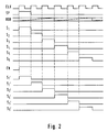
- Fig. 2 and Fig. 3 are timing charts in the sequential-sampling method and simultaneous-sampling method, respectively.
- the sampling pulse SP causes the shift stages SR 1 to SR n to shift an active high level or H-level in sequence in response to the clock signal CLK, so that the sampling signals S 1 to S n are outputted in sequence from the shift stages SR 1 to SR n , respectively.
- These sampling signals S 1 to S n are then entered into the logic gates G 1 to G n .
- the control signal EN since the control signal EN is at the H-level, the sampling signals S 1 to S n are directly transferred to the sample and hold circuits BF 1 to BF n with this timing as the signal S 1 ' to S n ', respectively.
- the display data signals R, G, B are sequentially sampled, so that then the sampled display data signals are supplied to the data buses Q 1 to Q n .
- the control pulse signal EN having a certain time period is inputted and the sampling start pulse signal SP having the pulse width equal to three time periods as large as the clock signal CLK is inputted. Accordingly, the sampling signals S 1 to S n having the pulse width equal to three time periods of the clock signal CLK are outputted from the shift stages SR 1 to SR n , respectively although these signals are supplied to the logic gates G 1 to G n of the timing selecting circuit, the control pulse signal EN causes three signals of the sampling signals S 1 ' to S n ' to be simultaneously outputted.
- the outputted three sampling signals S 1 ', S 2 ' and S 3 '; S 4 ' S 5 ' and S 6 ' and so on are transferred to the corresponding three ones of the sample/hole circuits BF 1 to BF n , so that three sets of the display data signals R, G and B are simultaneously sampled and thus transferred to the data buses Q 1 to Q n .
- this conventional data driver is applicable to both the sequential-sampling method and the simultaneous-sampling method.
- the pulse width of the sampling start pulse SP is required to be varied and the control pulse signal EN in synchronism with the clock signal CLK is also required to be changed.
- the external peripheral circuits for producing these signals SP and EN are made complicated.
- the widths of three sampling signal outputted from the timing selecting circuit are fluctuated. There are some possibilities that four sets of the sampling signals are outputted at the same time. The display data signal cannot be thereby correctly sampled.
- Another object of the present invention is to provide such a data driver for a matrix display device in which switching in mode between a sequential-sampling operation and a simultaneous-sampling operation is carried out without complicated peripheral circuits.
- a driver includes a shift register circuit for sequentially shifting a sampling start pulse in response to a clock signal to thereby produce a plurality of first sampling signals
- the shift register circuit comprising a plurality of shift registers (SR 1 -SR N ) each responsive to said clock signal, a plurality of sample/hole circuits each sampling display data in response to a second sampling signal supplied thereto and supplying the sampled data to a display device, and a switching circuit coupled between the shift register circuit and the sample/hold circuits and supplied with a control signal, said switching circuit transferring the sampling signals from the shift register circuit to the sample/hold circuits as said second sampling signal when said control signal is maintained at a first logic level, respectively, in a sequential-sampling mode and transferring when said control signal is maintained at a second logic level selected ones of the first sampling signals from the shift registers circuit to the sample/hole circuits such that each of the selected first sampling signals is transferred in common to two or more of the sample/hold circuits as the second sampling signals in a simultaneous
- a data driver 100 for a matrix display device includes n stages of shift registers SR 1 to SR n for sequentially shifting a sampling start pulse SP in response to a clock signal CLK.
- Each of the shift registers outputs associated two of sampling signals S 1 to S n with a relationship thereamong as shown in Fig. 6.
- the shift register SR 1 responds to the active high level of the sampling start pulse SR and generates the sampling signal S 1 in synchronous with the leading edge of the lock signal CLK and further generates the sampling signal S 2 in synchronism with the trailing edge thereof.
- the driver 100 further includes n stages of sample/hole circuits BF 1 to BF n each sampling an associated one of display data signals R, G and B under the control of an associated one of sampling control signals S 1 ' to S n ' and outputting the sampled data signal voltage to the corresponding one of data buses Q 1 to Q n .
- this data driver 100 is a sampling switching circuit TF which receives the sampling signals S 1 to S n outputted from the shift registers SR 1 to SR n and a sampling switching signal TFS and outputs the sampling control signals S 1 ' to S n ', through level shift circuits LS 1 to LS n .
- These level shift circuits LS 1 to LS n shift in level the sampling signals S 1 to S n to produce the sampling control signals S 1 ' to S n ' having a level suitable for driving the sample/hole circuits BF 1 to BF n .
- the sampling switching circuit includes a plurality of analog switches SWA 1 to SWA n and SWB 1 to SWB n which are arranged as shown in the drawing, and each of which consists, although not shown, of a p-channel MOS transistor and an n-channel MOS transistor connected in parallel to each other. If desired, each of the switch circuits SW can be composed of a transfer gate consisting of a single MOS transistor. Each of the switch circuits ASWA 1 to SWA n and BSWB 1 to SWB n is rendered conductive and non-conductive in accordance with the logic level of the sampling switching signal TFS.
- the H-level (high level) of the sampling switching signal TFS designates the sequential-sampling method and thus turns the switch circuits SWA 1 to SWA n ON and the switch circuits SWB 1 to SWB n OFF. Accordingly, as shown in Fig. 6, the sampling signals S 1 to S n outputted from the shift registers SR 1 to SR n passes through the sampling switching circuit TF as they are, and are then transferred via the level shift circuits LS 1 to LS n to the sample/hold circuits BS 1 to BF n as sampling signals S 1 ' to S n ' while keeping the present timings, respectively.
- the sample/hole circuits BF 1 to BF n sequentially sample display data signals R, G and B in response to the corresponding timings designated by the sampling signals S 1 ' to S n ', respectively.
- the display data signals thus sampled are then supplied to the data buses Q 1 to Q n .
- the sequential-sampling operation is thus performed.
- the sampling switching signal TFS is changed to be the L-level (low level).
- the switch circuits ASWA 1 to ASWA n are thereby turned OFF, whereas the switch circuits BSWB 1 to BWB n are turned ON.
- the same sampling signals S 1 to S n as those of Fig. 6 are derived from the shift registers SR 1 to SR n , sequential three ones of the sampling signals S 1 ' to S n ' are simultaneously outputted from the switching circuit TF at the same timings as those of the sampling signals S 2 , S 5 , S 8 , ---, S 3n-1 , respectively.
- the three ones of the sampling signals S 1 ' to S n ' thus output simultaneously are then transferred via the level shift circuits LS 1 to LS n to the corresponding three ones of the sample/hold circuits BF 1 to BF n .
- the three sets of the display data signals R, G, B are thereby sampled at the same time and then outputted to the corresponding ones of the data buses Q 1 to Q n .
- one of the sequential-sampling and simultaneous-sampling method is designated only by the level of the signal TFS. Moreover, this signal TFS is free from being synchronized with the clock signal CLK, and no change or control in level and is required to the signals SP and EN (Fig. 1). Accordingly, it is possible to realize the data driver for the matrix display device, capable of switching the sampling signals S 1 to S n outputted from the shift registers SR 1 to SR n and of being applied to any of the sequential-sampling method and the simultaneous-sampling method.
- a data driver 200 is constructed by employing such a sampling switching circuit TF that when a sampling switching signal TFS not synchronized with the clock signal CLK is inputted into this sampling switching circuit TF, the sampling signals S 1 to S n derived from the shift registers SR 1 to SR n and the sampling start pulse SP derived from the shift registers SR 2 , SR 4 , SR 6 , ---, SR 2n are switched. Accordingly, the sampling method of this data driver can be switched to either the sequential-sampling method or the simultaneous-sampling method.
- the switch circuits SWA 1 to SWA n are turned ON, whereas the switch circuits SWB 1 to SWB n are turned OFF. Therefore, the sampling signals S 1 ' to S n ' are generated in sequence, similarly to that of the first embodiment as represented in the timing chart of Fig. 6.
- both the sampling signals S 1 to S n outputted from the shift registers SR 1 to SR n and the sampling start pulse signal SP are switched, and the sampling signals S 1 ' to S n ' as indicated in Fig. 8 are transferred via the level shift circuits LS 1 to LS n to the sample/hole circuits BF 1 to BF n .
- the simultaneous-sampling method is thus performed with the sampling speed that is three times as high as that of the first embodiment.
- both the sampling signals S 1 to S n derived from the shift registers SR 1 to SR n and the sampling start pulse SP are switched in a similar manner to that of the first embodiment.
- the data driver for the matrix display device applicable to any of the sequential-sampling method and the simultaneous-sampling method.
- the data driver for the matrix-display device is provided with such a sampling switching circuit capable of switching both of the sampling signals derived from the shift registers and the sampling start pulse signal by inputting into this sampling switching circuit, the sampling switching signal with either the H-level or the L-level, which is not synchronized with the clock signal.
- the level shift circuits LS 1 to LS n may be omitted if the sampling signals derived from the switching circuit TF has a level sufficient to drive the sample/hold circuits BF 1 to BF n .
Landscapes
- Engineering & Computer Science (AREA)
- Theoretical Computer Science (AREA)
- Physics & Mathematics (AREA)
- General Physics & Mathematics (AREA)
- Computer Hardware Design (AREA)
- Human Computer Interaction (AREA)
- General Engineering & Computer Science (AREA)
- Control Of Indicators Other Than Cathode Ray Tubes (AREA)
- Liquid Crystal Display Device Control (AREA)
- Liquid Crystal (AREA)
- Transforming Electric Information Into Light Information (AREA)
Claims (6)
- Ein Datentreiber zum Abtasten von Anzeigedaten und Zuführen der abgetasteten Anzeigedaten (R, G, B) zu einer Anzeigevorrichtung, der folgendes aufweist:daß der Datentreiber (100) weiterhin folgendes aufweist:einen Schieberegister-Schaltkreis (SR) zum sequentiellen Verschieben eines Abtast-Startimpulses (SP) ansprechend auf ein Taktsignal (CLK), um dadurch eine Vielzahl von ersten Abtastsignalen (S1, ..., Sn) aufeinanderfolgend zu erzeugen;eine Vielzahl von Abtast/Halte-Schaltkreisen (BF1, ..., BFn) von denen jeder auf ein zugehöriges der zweiten Abtastsignale (S1', ..., Sn') anspricht, um die Anzeigedaten (R, G, B) abzutasten und abgetastete Anzeigedaten (Q1, ..., Qn') der Anzeigevorrichtung zuzuführen; unddadurch gekennzeichnet, daß der Schieberegister-Schaltkreis (SR) eine Vielzahl von Schieberegistern (SR1-SRn) aufweist, von denen jeder auf das Taktsignal (CLK) anspricht; undeinen Schalt-Schaltkreis (TF), der zwischen dem Schieberegister-Schaltkreis (SR) und den Abtast/Halte-Schaltkreisen (BF1, ..., BFn) angeschlossen ist und dem ein Steuersignal (TFS) zugeführt wird, wobei der Schalt-Schaltkreis (TF), wenn das Steuersignal (TFS) auf einem ersten logischen Pegel (HOCH) gehalten wird, die ersten Abtastsignale (S1, ..., Sn) als die jeweiligen zweiten Abtastsignale (S1', ..., Sn') auf die Abtast/Halte-Schaltkreise (BF1, ..., BFn) überträgt, und, wenn das Steuersignal (TFS) auf einem zweiten logischen Pegel (NIEDRIG) gehalten wird, ausgewählte erste Abtastsignale (S1, ..., Sn) überträgt, so daß jedes der ausgewählten ersten Abtastsignale (S1, ..., Sn) als die zweiten Abtastsignale (S1', ..., Sn') dieser gemeinsam auf zugehörige zwei oder mehr der Abtast/Halte-Schaltkreise (BF1, ..., BFn) übertragen wird.
- Datentreiber nach Anspruch 1, dadurch gekennzeichnet, daß der Schalt-Schaltkreis (TF) eine Vielzahl von Pegel-Schiebeschaltkreisen (LS1, ..., LSn) aufweist, von denen jeder einen Pegel von einem der ersten Abtastsignale (S1, ..., Sn), die diesem zugeführt werden, umwandelt und ein entsprechendes zweites Abtastsignal (S1', ..., Sn') erzeugt.
- Datentreiber nach Anspruch 1 oder 2, dadurch gekennzeichnet, daß der Schalt-Schaltkreis eine Vielzahl von analogen Schaltern (SWA1, ..., SWAn; SWB1, ..., SWBn) aufweist, von denen jeder aus einem P-Kanal-MOS-Transistor und einem N-Kanal-MOS-Transistor ausgebildet ist.
- Datentreiber nach Anspruch 1 oder 2, dadurch gekennzeichnet, daß der Schalt-Schaltkreis eine Vielzahl von Schalt-Schaltkreisen (SWA1, ..., SWAn; SWB1, ..., SWBn) aufweist, von denen jeder aus einem Übertragungsgate ausgebildet ist.
- Datentreiber nach einem der vorhergehenden Ansprüche, dadurch gekennzeichnet, daß der Schalt-Schaltkreis (TF) eine Vielzahl von Abtastsignal-Eingangsanschlüssen, denen jeweils die Vielzahl von ersten Abtastsignalen (S1, ..., Sn) zugeführt wird, eine Vielzahl von Abtast-Ausgangsanschlüssen und eine Vielzahl von Schaltern (SWA1, ···, ..., SWAn; SWB1, ..., SWBn) aufweist, die so angeordnet sind, daß die ersten der Schalter (SWA1, ..., SWAn) EINgeschaltet werden und die zweiten der Schalter (SWB1, ..., SWBn) AUSgeschaltet werden, wenn das Steuersignal (TFS) den ersten logischen Pegel (HOCH) einnimmt, um zu bewirken, daß die ersten Abtastsignale (S1, ..., Sn) als die jeweiligen zweiten Abtastsignale (S1', ..., Sn') an den Abtastsignal-Ausgangsanschlüssen erscheinen, und daß dritte der Schalter (SWB1, ..., SWBn) EINgeschaltet werden und vierte der Schalter (SWA1, ..., SWAn) AUSgeschaltet werden, wenn das Steuersignal (TFS) den zweiten logischen Pegel (NIEDRIG) einnimmt, um zu bewirken, daß mindestens eines der ersten Abtastsignale (S1, ..., Sn) als das zweite Abtastsignal (S1', ..., Sn') gemeinsam an zwei oder mehr der Abtast-Ausgangsanschlüsse erscheint.
- Datentreiber nach Anspruch 5, dadurch gekennzeichnet, daß die Vielzahl von Schaltern (SWA1, ..., SWAn; SWB1, ..., SWBn) eine Vielzahl von ersten Schaltern (SWA1, ..., SWAn), von denen jeder zwischen einem ausgewählten der ersten Abtastsignal-Eingangsanschlüsse und einem zugehörigen der Abtastsignal-Ausgangsanschlüsse angeschlossen ist, und eine Vielzahl von zweiten Schaltern (SWB1, ..., SWBn) aufweist, von denen jeder zwischen benachbarten Abtastsignal-Ausgangsanschlüssen angeschlossen ist.
Applications Claiming Priority (2)
| Application Number | Priority Date | Filing Date | Title |
|---|---|---|---|
| JP331705/93 | 1993-12-27 | ||
| JP5331705A JP2827867B2 (ja) | 1993-12-27 | 1993-12-27 | マトリックス表示装置のデータドライバ |
Publications (2)
| Publication Number | Publication Date |
|---|---|
| EP0660296A1 EP0660296A1 (de) | 1995-06-28 |
| EP0660296B1 true EP0660296B1 (de) | 1998-11-18 |
Family
ID=18246672
Family Applications (1)
| Application Number | Title | Priority Date | Filing Date |
|---|---|---|---|
| EP94120675A Expired - Lifetime EP0660296B1 (de) | 1993-12-27 | 1994-12-27 | Daten-Treiber zur Erzeugung zweier Sätze von Samplingsignalen für serielles Sampling und für simultanes Sampling |
Country Status (5)
| Country | Link |
|---|---|
| US (1) | US5682175A (de) |
| EP (1) | EP0660296B1 (de) |
| JP (1) | JP2827867B2 (de) |
| KR (1) | KR0176986B1 (de) |
| DE (1) | DE69414685T2 (de) |
Families Citing this family (37)
| Publication number | Priority date | Publication date | Assignee | Title |
|---|---|---|---|---|
| JP3329008B2 (ja) * | 1993-06-25 | 2002-09-30 | ソニー株式会社 | 双方向信号伝送回路網及び双方向信号転送シフトレジスタ |
| DE69533982T2 (de) * | 1994-11-21 | 2006-01-05 | Seiko Epson Corp. | Flüssigkristallsteuergerät, flüssigkristallanzeigegerät und flüssigkristallsteuerungsverfahren |
| JP3446209B2 (ja) * | 1995-02-01 | 2003-09-16 | セイコーエプソン株式会社 | 液晶表示装置、液晶表示装置の駆動方法、および液晶表示装置の検査方法 |
| JP3148972B2 (ja) * | 1995-06-01 | 2001-03-26 | キヤノン株式会社 | カラー表示装置の駆動回路 |
| DE69508443T2 (de) * | 1995-07-28 | 1999-07-08 | 1294339 Ontario, Inc., Toronto, Ontario | Integrierte analogische quellensteuerschaltung für ein flüssigkristallanzeige mit aktiver matrix |
| KR100264506B1 (ko) * | 1995-08-30 | 2000-09-01 | 야스카와 히데아키 | 화상 표시 장치와 화상 표시 방법과 표시 구동 장치와 이를 이용한 전자기기 |
| JP3518086B2 (ja) * | 1995-09-07 | 2004-04-12 | ソニー株式会社 | 映像信号処理装置 |
| JP3330812B2 (ja) * | 1996-03-22 | 2002-09-30 | シャープ株式会社 | マトリックス型表示装置およびその駆動方法 |
| JPH09258700A (ja) * | 1996-03-22 | 1997-10-03 | Toshiba Electron Eng Corp | 液晶表示装置の駆動回路 |
| JP2923906B2 (ja) * | 1996-06-07 | 1999-07-26 | 日本電気株式会社 | 液晶表示装置の駆動回路 |
| TW317354U (en) * | 1996-09-10 | 1997-10-01 | Ind Tech Res Inst | Thin film transistor liquid crystal driving device |
| KR100240278B1 (ko) * | 1997-02-14 | 2000-01-15 | 김영환 | 엘시디 드라이버용 클럭발생회로 |
| TW440742B (en) * | 1997-03-03 | 2001-06-16 | Toshiba Corp | Flat panel display device |
| US6124840A (en) * | 1997-04-07 | 2000-09-26 | Hyundai Electronics Industries Co., Ltd. | Low power gate driver circuit for thin film transistor-liquid crystal display (TFT-LCD) using electric charge recycling technique |
| US7304632B2 (en) * | 1997-05-13 | 2007-12-04 | Oki Electric Industry Co., Ltd. | Liquid-crystal display driving circuit and method |
| JP3148151B2 (ja) * | 1997-05-27 | 2001-03-19 | 日本電気株式会社 | 液晶駆動装置の出力偏差低減方法および装置 |
| JPH11133926A (ja) * | 1997-10-30 | 1999-05-21 | Hitachi Ltd | 半導体集積回路装置および液晶表示装置 |
| JP3024618B2 (ja) * | 1997-11-19 | 2000-03-21 | 日本電気株式会社 | 液晶駆動回路 |
| WO1999028896A1 (en) * | 1997-11-28 | 1999-06-10 | Seiko Epson Corporation | Drive circuit for electro-optic apparatus, method of driving the electro-optic apparatus, electro-optic apparatus, and electronic apparatus |
| JPH11272226A (ja) * | 1998-03-24 | 1999-10-08 | Sharp Corp | データ信号線駆動回路及び画像表示装置 |
| JP2000267616A (ja) * | 1999-03-19 | 2000-09-29 | Sony Corp | 液晶表示装置およびその駆動方法 |
| US6476790B1 (en) * | 1999-08-18 | 2002-11-05 | Semiconductor Energy Laboratory Co., Ltd. | Display device and a driver circuit thereof |
| US6515648B1 (en) * | 1999-08-31 | 2003-02-04 | Semiconductor Energy Laboratory Co., Ltd. | Shift register circuit, driving circuit of display device, and display device using the driving circuit |
| US6518800B2 (en) * | 2000-05-31 | 2003-02-11 | Texas Instruments Incorporated | System and method for reducing timing mismatch in sample and hold circuits using the clock |
| JP2002203397A (ja) * | 2000-10-24 | 2002-07-19 | Alps Electric Co Ltd | シフトレジスタ回路、表示装置およびイメージセンサ |
| KR100759974B1 (ko) * | 2001-02-26 | 2007-09-18 | 삼성전자주식회사 | 액정 표시 장치 및 그의 구동 방법. |
| KR100922790B1 (ko) * | 2003-02-28 | 2009-10-21 | 엘지디스플레이 주식회사 | 액정 패널의 게이트 구동 장치 |
| JP4007239B2 (ja) | 2003-04-08 | 2007-11-14 | ソニー株式会社 | 表示装置 |
| US6937687B2 (en) * | 2003-10-21 | 2005-08-30 | Au Optronics Corporation | Bi-directional shift register control circuit |
| US7280063B2 (en) * | 2005-04-29 | 2007-10-09 | Georgia Tech Research Corporation | Programmable voltage-output floating-gate digital to analog converter and tunable resistors |
| WO2007022386A2 (en) * | 2005-08-17 | 2007-02-22 | Georgia Tech Research Corporation | A reconfigurable mixed-signal vlsi implementation of distributed arithmetic |
| KR100662977B1 (ko) | 2005-10-25 | 2006-12-28 | 삼성에스디아이 주식회사 | 쉬프트 레지스터 및 이를 이용한 유기 발광 표시장치 |
| US7656381B2 (en) * | 2006-01-11 | 2010-02-02 | Tpo Displays Corp. | Systems for providing dual resolution control of display panels |
| WO2007135805A1 (ja) * | 2006-05-24 | 2007-11-29 | Sharp Kabushiki Kaisha | 表示パネル駆動回路、表示装置 |
| JP5057335B2 (ja) * | 2008-03-24 | 2012-10-24 | 株式会社ジャパンディスプレイウェスト | 表示装置 |
| TW201235995A (en) * | 2011-02-18 | 2012-09-01 | Novatek Microelectronics Corp | Display driving circuit and method |
| CN108831370B (zh) * | 2018-08-28 | 2021-11-19 | 京东方科技集团股份有限公司 | 显示驱动方法及其装置、显示装置和可穿戴设备 |
Family Cites Families (6)
| Publication number | Priority date | Publication date | Assignee | Title |
|---|---|---|---|---|
| JPH06101848B2 (ja) * | 1985-08-12 | 1994-12-12 | 松下電器産業株式会社 | 画像表示装置 |
| JPH0654421B2 (ja) * | 1987-12-07 | 1994-07-20 | シャープ株式会社 | マトリクス型液晶表示装置の列電極駆動回路 |
| JPH0221499A (ja) * | 1988-07-07 | 1990-01-24 | Toshiba Corp | サンプルホールド回路 |
| US5061920A (en) * | 1988-12-20 | 1991-10-29 | Honeywell Inc. | Saturating column driver for grey scale LCD |
| JPH04179996A (ja) * | 1990-11-15 | 1992-06-26 | Toshiba Corp | サンプルホールド回路およびこれを用いた液晶ディスプレイ装置 |
| JP3202384B2 (ja) * | 1993-02-22 | 2001-08-27 | シャープ株式会社 | 表示装置の駆動回路 |
-
1993
- 1993-12-27 JP JP5331705A patent/JP2827867B2/ja not_active Expired - Fee Related
-
1994
- 1994-12-22 US US08/361,973 patent/US5682175A/en not_active Expired - Fee Related
- 1994-12-27 EP EP94120675A patent/EP0660296B1/de not_active Expired - Lifetime
- 1994-12-27 KR KR1019940037108A patent/KR0176986B1/ko not_active Expired - Fee Related
- 1994-12-27 DE DE69414685T patent/DE69414685T2/de not_active Expired - Fee Related
Also Published As
| Publication number | Publication date |
|---|---|
| DE69414685D1 (de) | 1998-12-24 |
| JPH07191624A (ja) | 1995-07-28 |
| US5682175A (en) | 1997-10-28 |
| KR0176986B1 (ko) | 1999-05-15 |
| EP0660296A1 (de) | 1995-06-28 |
| JP2827867B2 (ja) | 1998-11-25 |
| KR950020069A (ko) | 1995-07-24 |
| DE69414685T2 (de) | 1999-06-24 |
Similar Documents
| Publication | Publication Date | Title |
|---|---|---|
| EP0660296B1 (de) | Daten-Treiber zur Erzeugung zweier Sätze von Samplingsignalen für serielles Sampling und für simultanes Sampling | |
| EP0553823B1 (de) | Horizontal-Treiberschaltung mit Eliminierungsfunktion fixer Muster | |
| US5572211A (en) | Integrated circuit for driving liquid crystal display using multi-level D/A converter | |
| US6335721B1 (en) | LCD source driver | |
| EP0861484B1 (de) | Integrierte Schaltung zur Steuerung einer Flüssigkristallanzeigevorrichtung mit Pixelinvertierung | |
| US7274351B2 (en) | Driver circuit and shift register of display device and display device | |
| KR950010135B1 (ko) | 디스플레이 장치용 열 전극 구동회로 | |
| JP2862592B2 (ja) | ディスプレイ装置 | |
| US6963327B2 (en) | Shift register circuit including first shift register having plurality of stages connected in cascade and second shift register having more stages | |
| JP2003228339A (ja) | 液晶表示装置およびその駆動方法 | |
| US4785297A (en) | Driver circuit for matrix type display device | |
| US5369417A (en) | Sample and hold circuit being arranged for easily changing phases of shift clocks | |
| JPH10260661A (ja) | 表示装置の駆動回路 | |
| JPH02894A (ja) | 表示装置をアドレス指定する装置及び方法 | |
| JP3755360B2 (ja) | 電気光学装置の駆動回路及びこれを用いた電気光学装置、電子機器、及び電気光学装置の制御信号の位相調整装置、並びに制御信号の位相調整方法 | |
| JP4993885B2 (ja) | マルチチャネルシフトレジスタ及びそれを備えるソースドライバ | |
| US20020093497A1 (en) | Scanning circuit , and imaging apparatus having the same | |
| JP2000250495A (ja) | 液晶表示パネルのデータ線駆動装置 | |
| JPH02210323A (ja) | マトリクス回路の駆動回路及びその駆動回路を制御するクロック形成器 | |
| JP3326639B2 (ja) | オーバーラップ除去機能付双方向走査回路 | |
| EP0544427B1 (de) | Steuerschaltung für eine Anzeigeeinheit mit digitaler Sourcesteuerung zur Erzeugung von Mehrfachpegelsteuerspannungen aus einer einzelnen externen Energiequelle | |
| US5099502A (en) | Shift register for producing pulses in sequence | |
| JP3322011B2 (ja) | カラー表示システム | |
| KR100497000B1 (ko) | 피디피구동장치의칼럼드라이버구동회로 | |
| JPH06348232A (ja) | 液晶表示パネル駆動回路 |
Legal Events
| Date | Code | Title | Description |
|---|---|---|---|
| PUAI | Public reference made under article 153(3) epc to a published international application that has entered the european phase |
Free format text: ORIGINAL CODE: 0009012 |
|
| AK | Designated contracting states |
Kind code of ref document: A1 Designated state(s): DE FR GB |
|
| 17P | Request for examination filed |
Effective date: 19951228 |
|
| 17Q | First examination report despatched |
Effective date: 19970513 |
|
| GRAG | Despatch of communication of intention to grant |
Free format text: ORIGINAL CODE: EPIDOS AGRA |
|
| GRAG | Despatch of communication of intention to grant |
Free format text: ORIGINAL CODE: EPIDOS AGRA |
|
| GRAH | Despatch of communication of intention to grant a patent |
Free format text: ORIGINAL CODE: EPIDOS IGRA |
|
| GRAH | Despatch of communication of intention to grant a patent |
Free format text: ORIGINAL CODE: EPIDOS IGRA |
|
| GRAA | (expected) grant |
Free format text: ORIGINAL CODE: 0009210 |
|
| AK | Designated contracting states |
Kind code of ref document: B1 Designated state(s): DE FR GB |
|
| REF | Corresponds to: |
Ref document number: 69414685 Country of ref document: DE Date of ref document: 19981224 |
|
| ET | Fr: translation filed | ||
| PLBE | No opposition filed within time limit |
Free format text: ORIGINAL CODE: 0009261 |
|
| STAA | Information on the status of an ep patent application or granted ep patent |
Free format text: STATUS: NO OPPOSITION FILED WITHIN TIME LIMIT |
|
| 26N | No opposition filed | ||
| REG | Reference to a national code |
Ref country code: GB Ref legal event code: IF02 |
|
| REG | Reference to a national code |
Ref country code: GB Ref legal event code: 732E |
|
| REG | Reference to a national code |
Ref country code: FR Ref legal event code: TP |
|
| PGFP | Annual fee paid to national office [announced via postgrant information from national office to epo] |
Ref country code: FR Payment date: 20061208 Year of fee payment: 13 |
|
| PGFP | Annual fee paid to national office [announced via postgrant information from national office to epo] |
Ref country code: DE Payment date: 20061221 Year of fee payment: 13 |
|
| PGFP | Annual fee paid to national office [announced via postgrant information from national office to epo] |
Ref country code: GB Payment date: 20061227 Year of fee payment: 13 |
|
| GBPC | Gb: european patent ceased through non-payment of renewal fee |
Effective date: 20071227 |
|
| PG25 | Lapsed in a contracting state [announced via postgrant information from national office to epo] |
Ref country code: DE Free format text: LAPSE BECAUSE OF NON-PAYMENT OF DUE FEES Effective date: 20080701 |
|
| REG | Reference to a national code |
Ref country code: FR Ref legal event code: ST Effective date: 20081020 |
|
| PG25 | Lapsed in a contracting state [announced via postgrant information from national office to epo] |
Ref country code: GB Free format text: LAPSE BECAUSE OF NON-PAYMENT OF DUE FEES Effective date: 20071227 |
|
| PG25 | Lapsed in a contracting state [announced via postgrant information from national office to epo] |
Ref country code: FR Free format text: LAPSE BECAUSE OF NON-PAYMENT OF DUE FEES Effective date: 20071231 |