EP0628997A2 - Halbleiteranordnung mit schmallem Träger und Herstellungsverfahren - Google Patents
Halbleiteranordnung mit schmallem Träger und Herstellungsverfahren Download PDFInfo
- Publication number
- EP0628997A2 EP0628997A2 EP94304221A EP94304221A EP0628997A2 EP 0628997 A2 EP0628997 A2 EP 0628997A2 EP 94304221 A EP94304221 A EP 94304221A EP 94304221 A EP94304221 A EP 94304221A EP 0628997 A2 EP0628997 A2 EP 0628997A2
- Authority
- EP
- European Patent Office
- Prior art keywords
- mounting pad
- mounting
- semiconductor device
- lead frame
- chip
- Prior art date
- Legal status (The legal status is an assumption and is not a legal conclusion. Google has not performed a legal analysis and makes no representation as to the accuracy of the status listed.)
- Granted
Links
Images


Classifications
-
- H—ELECTRICITY
- H10—SEMICONDUCTOR DEVICES; ELECTRIC SOLID-STATE DEVICES NOT OTHERWISE PROVIDED FOR
- H10W—GENERIC PACKAGES, INTERCONNECTIONS, CONNECTORS OR OTHER CONSTRUCTIONAL DETAILS OF DEVICES COVERED BY CLASS H10
- H10W70/00—Package substrates; Interposers; Redistribution layers [RDL]
- H10W70/40—Leadframes
- H10W70/411—Chip-supporting parts, e.g. die pads
-
- H—ELECTRICITY
- H10—SEMICONDUCTOR DEVICES; ELECTRIC SOLID-STATE DEVICES NOT OTHERWISE PROVIDED FOR
- H10W—GENERIC PACKAGES, INTERCONNECTIONS, CONNECTORS OR OTHER CONSTRUCTIONAL DETAILS OF DEVICES COVERED BY CLASS H10
- H10W70/00—Package substrates; Interposers; Redistribution layers [RDL]
- H10W70/01—Manufacture or treatment
- H10W70/04—Manufacture or treatment of leadframes
-
- H—ELECTRICITY
- H10—SEMICONDUCTOR DEVICES; ELECTRIC SOLID-STATE DEVICES NOT OTHERWISE PROVIDED FOR
- H10W—GENERIC PACKAGES, INTERCONNECTIONS, CONNECTORS OR OTHER CONSTRUCTIONAL DETAILS OF DEVICES COVERED BY CLASS H10
- H10W72/00—Interconnections or connectors in packages
- H10W72/01—Manufacture or treatment
- H10W72/015—Manufacture or treatment of bond wires
-
- H—ELECTRICITY
- H10—SEMICONDUCTOR DEVICES; ELECTRIC SOLID-STATE DEVICES NOT OTHERWISE PROVIDED FOR
- H10W—GENERIC PACKAGES, INTERCONNECTIONS, CONNECTORS OR OTHER CONSTRUCTIONAL DETAILS OF DEVICES COVERED BY CLASS H10
- H10W72/00—Interconnections or connectors in packages
- H10W72/50—Bond wires
-
- H—ELECTRICITY
- H10—SEMICONDUCTOR DEVICES; ELECTRIC SOLID-STATE DEVICES NOT OTHERWISE PROVIDED FOR
- H10W—GENERIC PACKAGES, INTERCONNECTIONS, CONNECTORS OR OTHER CONSTRUCTIONAL DETAILS OF DEVICES COVERED BY CLASS H10
- H10W90/00—Package configurations
- H10W90/811—Multiple chips on leadframes
-
- H—ELECTRICITY
- H10—SEMICONDUCTOR DEVICES; ELECTRIC SOLID-STATE DEVICES NOT OTHERWISE PROVIDED FOR
- H10W—GENERIC PACKAGES, INTERCONNECTIONS, CONNECTORS OR OTHER CONSTRUCTIONAL DETAILS OF DEVICES COVERED BY CLASS H10
- H10W72/00—Interconnections or connectors in packages
- H10W72/01—Manufacture or treatment
- H10W72/013—Manufacture or treatment of die-attach connectors
- H10W72/01308—Manufacture or treatment of die-attach connectors using permanent auxiliary members, e.g. using alignment marks
-
- H—ELECTRICITY
- H10—SEMICONDUCTOR DEVICES; ELECTRIC SOLID-STATE DEVICES NOT OTHERWISE PROVIDED FOR
- H10W—GENERIC PACKAGES, INTERCONNECTIONS, CONNECTORS OR OTHER CONSTRUCTIONAL DETAILS OF DEVICES COVERED BY CLASS H10
- H10W72/00—Interconnections or connectors in packages
- H10W72/071—Connecting or disconnecting
- H10W72/0711—Apparatus therefor
- H10W72/07141—Means for applying energy, e.g. ovens or lasers
-
- H—ELECTRICITY
- H10—SEMICONDUCTOR DEVICES; ELECTRIC SOLID-STATE DEVICES NOT OTHERWISE PROVIDED FOR
- H10W—GENERIC PACKAGES, INTERCONNECTIONS, CONNECTORS OR OTHER CONSTRUCTIONAL DETAILS OF DEVICES COVERED BY CLASS H10
- H10W72/00—Interconnections or connectors in packages
- H10W72/071—Connecting or disconnecting
- H10W72/073—Connecting or disconnecting of die-attach connectors
- H10W72/07321—Aligning
- H10W72/07327—Aligning involving guiding structures, e.g. spacers or supporting members
-
- H—ELECTRICITY
- H10—SEMICONDUCTOR DEVICES; ELECTRIC SOLID-STATE DEVICES NOT OTHERWISE PROVIDED FOR
- H10W—GENERIC PACKAGES, INTERCONNECTIONS, CONNECTORS OR OTHER CONSTRUCTIONAL DETAILS OF DEVICES COVERED BY CLASS H10
- H10W72/00—Interconnections or connectors in packages
- H10W72/071—Connecting or disconnecting
- H10W72/073—Connecting or disconnecting of die-attach connectors
- H10W72/07351—Connecting or disconnecting of die-attach connectors characterised by changes in properties of the die-attach connectors during connecting
- H10W72/07352—Connecting or disconnecting of die-attach connectors characterised by changes in properties of the die-attach connectors during connecting changes in structures or sizes
-
- H—ELECTRICITY
- H10—SEMICONDUCTOR DEVICES; ELECTRIC SOLID-STATE DEVICES NOT OTHERWISE PROVIDED FOR
- H10W—GENERIC PACKAGES, INTERCONNECTIONS, CONNECTORS OR OTHER CONSTRUCTIONAL DETAILS OF DEVICES COVERED BY CLASS H10
- H10W72/00—Interconnections or connectors in packages
- H10W72/071—Connecting or disconnecting
- H10W72/073—Connecting or disconnecting of die-attach connectors
- H10W72/07351—Connecting or disconnecting of die-attach connectors characterised by changes in properties of the die-attach connectors during connecting
- H10W72/07353—Connecting or disconnecting of die-attach connectors characterised by changes in properties of the die-attach connectors during connecting changes in shapes
-
- H—ELECTRICITY
- H10—SEMICONDUCTOR DEVICES; ELECTRIC SOLID-STATE DEVICES NOT OTHERWISE PROVIDED FOR
- H10W—GENERIC PACKAGES, INTERCONNECTIONS, CONNECTORS OR OTHER CONSTRUCTIONAL DETAILS OF DEVICES COVERED BY CLASS H10
- H10W72/00—Interconnections or connectors in packages
- H10W72/071—Connecting or disconnecting
- H10W72/075—Connecting or disconnecting of bond wires
- H10W72/07521—Aligning
-
- H—ELECTRICITY
- H10—SEMICONDUCTOR DEVICES; ELECTRIC SOLID-STATE DEVICES NOT OTHERWISE PROVIDED FOR
- H10W—GENERIC PACKAGES, INTERCONNECTIONS, CONNECTORS OR OTHER CONSTRUCTIONAL DETAILS OF DEVICES COVERED BY CLASS H10
- H10W72/00—Interconnections or connectors in packages
- H10W72/071—Connecting or disconnecting
- H10W72/075—Connecting or disconnecting of bond wires
- H10W72/07531—Techniques
- H10W72/07532—Compression bonding, e.g. thermocompression bonding
- H10W72/07533—Ultrasonic bonding, e.g. thermosonic bonding
-
- H—ELECTRICITY
- H10—SEMICONDUCTOR DEVICES; ELECTRIC SOLID-STATE DEVICES NOT OTHERWISE PROVIDED FOR
- H10W—GENERIC PACKAGES, INTERCONNECTIONS, CONNECTORS OR OTHER CONSTRUCTIONAL DETAILS OF DEVICES COVERED BY CLASS H10
- H10W72/00—Interconnections or connectors in packages
- H10W72/30—Die-attach connectors
- H10W72/321—Structures or relative sizes of die-attach connectors
-
- H—ELECTRICITY
- H10—SEMICONDUCTOR DEVICES; ELECTRIC SOLID-STATE DEVICES NOT OTHERWISE PROVIDED FOR
- H10W—GENERIC PACKAGES, INTERCONNECTIONS, CONNECTORS OR OTHER CONSTRUCTIONAL DETAILS OF DEVICES COVERED BY CLASS H10
- H10W72/00—Interconnections or connectors in packages
- H10W72/30—Die-attach connectors
- H10W72/331—Shapes of die-attach connectors
- H10W72/332—Plan-view shape, i.e. in top view
-
- H—ELECTRICITY
- H10—SEMICONDUCTOR DEVICES; ELECTRIC SOLID-STATE DEVICES NOT OTHERWISE PROVIDED FOR
- H10W—GENERIC PACKAGES, INTERCONNECTIONS, CONNECTORS OR OTHER CONSTRUCTIONAL DETAILS OF DEVICES COVERED BY CLASS H10
- H10W72/00—Interconnections or connectors in packages
- H10W72/50—Bond wires
- H10W72/531—Shapes of wire connectors
- H10W72/536—Shapes of wire connectors the connected ends being ball-shaped
-
- H—ELECTRICITY
- H10—SEMICONDUCTOR DEVICES; ELECTRIC SOLID-STATE DEVICES NOT OTHERWISE PROVIDED FOR
- H10W—GENERIC PACKAGES, INTERCONNECTIONS, CONNECTORS OR OTHER CONSTRUCTIONAL DETAILS OF DEVICES COVERED BY CLASS H10
- H10W72/00—Interconnections or connectors in packages
- H10W72/50—Bond wires
- H10W72/531—Shapes of wire connectors
- H10W72/5363—Shapes of wire connectors the connected ends being wedge-shaped
-
- H—ELECTRICITY
- H10—SEMICONDUCTOR DEVICES; ELECTRIC SOLID-STATE DEVICES NOT OTHERWISE PROVIDED FOR
- H10W—GENERIC PACKAGES, INTERCONNECTIONS, CONNECTORS OR OTHER CONSTRUCTIONAL DETAILS OF DEVICES COVERED BY CLASS H10
- H10W72/00—Interconnections or connectors in packages
- H10W72/50—Bond wires
- H10W72/551—Materials of bond wires
- H10W72/552—Materials of bond wires comprising metals or metalloids, e.g. silver
- H10W72/5522—Materials of bond wires comprising metals or metalloids, e.g. silver comprising gold [Au]
-
- H—ELECTRICITY
- H10—SEMICONDUCTOR DEVICES; ELECTRIC SOLID-STATE DEVICES NOT OTHERWISE PROVIDED FOR
- H10W—GENERIC PACKAGES, INTERCONNECTIONS, CONNECTORS OR OTHER CONSTRUCTIONAL DETAILS OF DEVICES COVERED BY CLASS H10
- H10W72/00—Interconnections or connectors in packages
- H10W72/851—Dispositions of multiple connectors or interconnections
- H10W72/874—On different surfaces
- H10W72/884—Die-attach connectors and bond wires
-
- H—ELECTRICITY
- H10—SEMICONDUCTOR DEVICES; ELECTRIC SOLID-STATE DEVICES NOT OTHERWISE PROVIDED FOR
- H10W—GENERIC PACKAGES, INTERCONNECTIONS, CONNECTORS OR OTHER CONSTRUCTIONAL DETAILS OF DEVICES COVERED BY CLASS H10
- H10W74/00—Encapsulations, e.g. protective coatings
-
- H—ELECTRICITY
- H10—SEMICONDUCTOR DEVICES; ELECTRIC SOLID-STATE DEVICES NOT OTHERWISE PROVIDED FOR
- H10W—GENERIC PACKAGES, INTERCONNECTIONS, CONNECTORS OR OTHER CONSTRUCTIONAL DETAILS OF DEVICES COVERED BY CLASS H10
- H10W90/00—Package configurations
- H10W90/701—Package configurations characterised by the relative positions of pads or connectors relative to package parts
- H10W90/731—Package configurations characterised by the relative positions of pads or connectors relative to package parts of die-attach connectors
- H10W90/736—Package configurations characterised by the relative positions of pads or connectors relative to package parts of die-attach connectors between a chip and a stacked lead frame, conducting package substrate or heat sink
-
- H—ELECTRICITY
- H10—SEMICONDUCTOR DEVICES; ELECTRIC SOLID-STATE DEVICES NOT OTHERWISE PROVIDED FOR
- H10W—GENERIC PACKAGES, INTERCONNECTIONS, CONNECTORS OR OTHER CONSTRUCTIONAL DETAILS OF DEVICES COVERED BY CLASS H10
- H10W90/00—Package configurations
- H10W90/701—Package configurations characterised by the relative positions of pads or connectors relative to package parts
- H10W90/751—Package configurations characterised by the relative positions of pads or connectors relative to package parts of bond wires
- H10W90/756—Package configurations characterised by the relative positions of pads or connectors relative to package parts of bond wires between a chip and a stacked lead frame, conducting package substrate or heat sink
-
- Y—GENERAL TAGGING OF NEW TECHNOLOGICAL DEVELOPMENTS; GENERAL TAGGING OF CROSS-SECTIONAL TECHNOLOGIES SPANNING OVER SEVERAL SECTIONS OF THE IPC; TECHNICAL SUBJECTS COVERED BY FORMER USPC CROSS-REFERENCE ART COLLECTIONS [XRACs] AND DIGESTS
- Y10—TECHNICAL SUBJECTS COVERED BY FORMER USPC
- Y10T—TECHNICAL SUBJECTS COVERED BY FORMER US CLASSIFICATION
- Y10T29/00—Metal working
- Y10T29/49—Method of mechanical manufacture
- Y10T29/49002—Electrical device making
- Y10T29/49117—Conductor or circuit manufacturing
- Y10T29/49121—Beam lead frame or beam lead device
-
- Y—GENERAL TAGGING OF NEW TECHNOLOGICAL DEVELOPMENTS; GENERAL TAGGING OF CROSS-SECTIONAL TECHNOLOGIES SPANNING OVER SEVERAL SECTIONS OF THE IPC; TECHNICAL SUBJECTS COVERED BY FORMER USPC CROSS-REFERENCE ART COLLECTIONS [XRACs] AND DIGESTS
- Y10—TECHNICAL SUBJECTS COVERED BY FORMER USPC
- Y10T—TECHNICAL SUBJECTS COVERED BY FORMER US CLASSIFICATION
- Y10T29/00—Metal working
- Y10T29/49—Method of mechanical manufacture
- Y10T29/49002—Electrical device making
- Y10T29/49117—Conductor or circuit manufacturing
- Y10T29/49124—On flat or curved insulated base, e.g., printed circuit, etc.
- Y10T29/4913—Assembling to base an electrical component, e.g., capacitor, etc.
- Y10T29/49146—Assembling to base an electrical component, e.g., capacitor, etc. with encapsulating, e.g., potting, etc.
Definitions
- This invention relates to a semiconductor device, in particular, a package structure in which a semiconductor integrated circuit (IC) chip is sealed in resin, the manufacturing method of making same, and a lead frame.
- IC semiconductor integrated circuit
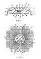
- the lead frame material 1 is formed entirely of metal (e.g., 42 alloy, copper alloy, copper, etc.), and lead frame outerframe 2 and lead frame part 8 having a plurality of inner leads 7 extending radially in four directions in the inside position are formed as one body by etching, etc.
- metal e.g., 42 alloy, copper alloy, copper, etc.
- outer leads 6 are connected by linear connection parts (dumb bar) 9 at each side and the connection parts are integrated to outer frame 2 with each corner part of lead frame part 8.
- IC chip 10 is mounted on a square shaped mounting pad (die pad) 11 having a larger area than the area of IC chip 10.
- Support pins 12 which support the mounting pad 11 are provided on the mounting pad 11 and are integrated with outer frame 2 at the corner parts. 4 in the figure is the hole for positioning the lead frame material.
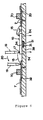
- Semiconductor package 13 which is fixed, wire bonded, and resin-sealed as shown in Figures 22-24 using the lead frame material 1, is mounted (fixed) with silver paste 14 on mounting pad 11 as shown in Figures 19-21.
- Pad 17 is bonded to inner lead 7 with wire 15, and structured to be totally sealed with resin 16 such as epoxy, etc.
- the alternating long and short dashed line indicates the outer line of sealing resin 16 and alternating long and two short-dashed line indicates the position of IC chip 10.
- IC chip 10 is mounted with silver paste 14 on mounting pad 11 as shown in the enlarged figure of Figure 22.
- heater member (heater insert or heater block) 18 is contacted to mounting pad 11 from the bottom side during the wire bonding as shown in Figure 23 so that heat of the heater is conducted to the bonding pad (pad 17) simultaneous with supporting mounting pad 11.
- Wire bonding is executed by coupling wire 15 to bonding pad 17 with capillary 19 while providing thermal and ultrasonic energy, guiding it to inner lead 7 as indicated by arrow 20, then cladding it.
- mounting pad 11 of IC chip 10 was formed to be larger than IC chip 10, but this was mainly due to the following reasons.
- mounting pad 11 is made smaller than IC chip 10 as shown in Figure 24 during the bonding, the peripheral part of mounting pad 11 does not contact heater insert 18, so IC chip 10 slants during the ultrasonic function based on capillary 19, the support becomes unstable, ultrasonic energy cannot be used effectively, and the heat from heater insert 18 is not conducted efficiently to IC chip 10. Thus imperfect bonding is executed. Therefore, making the mounting pad 11 smaller than IC chip 10 was considered by those in the industry to be impractical and undesirable.
- solder 23 is fused by solder reflow (e.g., IR reflow by infrared irradiation) then solidified, but cracks 24 may be created in resin 16 as shown in the figures.
- solder reflow e.g., IR reflow by infrared irradiation
- silver paste 14 for fixing IC chip 10 is a material with very high hygroscopicity, such that the hygroscopic moisture may cause vapor explosion during the heating such as IR reflow, etc.
- pad 11 is deformed by the condensed water causing vapor explosion due to a phenomenon similar to the above-mentioned in the part with silver paste 14, great stress is applied to resin 16, and cracks 24 are created in particular from edge 11 a of pad 11.
- the present invention relates to a semiconductor package device in which a semiconductor element is sealed in resin and fixed to a mounting part (e.g., a mounting pad and/or an additional mounting part for the support pins) which is smaller than the semiconductor element, and a lead frame with the mounting part.
- a mounting part e.g., a mounting pad and/or an additional mounting part for the support pins
- a concave part in the semiconductor device package and lead frame of the present invention, it is preferable for a concave part to be formed on the mount surface of the mounting pad and for the concave part to be filled with a fixing agent for semiconductor element fixation. Also, it is preferable for the side surface of the mounting pad to be slanted inwardly from the semiconductor element mount surface toward the opposite surface.
- the side surface of the support pin which supports the mounting pad is slanted inward from the semiconductor element mount side toward the opposite surface.
- additional mounting parts it is possible for additional mounting parts to be provided to the support pin, and to fix semiconductor elements even on this mounting part.
- the concave part it is preferable for the concave part to be formed in the additional mounting part of the support pin and to fill the concave part with a fixing agent for semiconductor element fixation.
- the semiconductor device package of the present invention prefferably be manufactured by the method of inserting a mounting pad and/or support pin in the insertion concave part formed on the heater member with respect to the lead frame (in particular, a lead frame with a mounting pad smaller than the semiconductor element), and in this state, contacting the heater member to the back surface of the semiconductor element fixed to the mounting pad and/or support pin, and bonding the inner lead of the lead frame to the semiconductor element.
- the heater member used in the manufacturing method it is preferable to also form an insertion concave part for the support pins of the mounting pad. Also, it is preferable to make the mounting pad insertion concave part to be larger than the mounting pad.
- Figures 1-8 show a first embodiment of the present invention.
- the parts common to the conventional semiconductor device package explained earlier are designated with the same reference numerals and the description thereof may be omitted.
- other features include a square-shaped concave part 30 formed on the chip mounting surface of the mounting pad 31, and a fixing agent 34 such as silver paste, etc., filling in the concave part for fixation of the IC chip 10, wherein the fixing agent 34 is not adhered to the junction part 50 of IC chip 10 and mounting pad 31 (namely, the fixation surface of fixing agent 34 exists within more or less the same plane as the mounting surface of mounting pad 31).
- a fixing agent 34 such as silver paste, etc.
- the area of mounting pad 31 can be 15-40% of the chip size of IC chip 10 but when the stress, influenced by the silver paste quantity, and displacement in the position of IC chip 10 during handling, which will be discussed later, are considered, the smaller the better. For example, when the size of IC chip 10 is 8 mm x 8 mm, a mounting pad 31 of about 4 mm x 4 mm (about 25% of the area of IC chip 10) is considered suitable.
- This type of mounting pad 31 is formed as one body by etching, etc., as part of the lead frame 41 as shown in Figure 5 along with support pins 32 (furthermore, leads 6 and 7, etc.).
- Concave part 30 of mounting pad 31 can be formed by partial etching as indicated in Figure 3 and the depth d can be the thickness (e.g., about 30 f..lm) of silver paste 34 as shown in Figure 4.
- one corner part (the corner part at the top left in Figure 5) of the four corner parts of lead frame part 8 is directly fixed to an outer frame 2 of the lead frame 41 as in Figure 21 and the other three corner parts are respectively connected to the outer frame 2 of the lead frame 41 through three snake- shaped bent parts 22, 23, and 24.
- the warpage stress which may be generated in directions such as vertical, horizontal, etc., is effectively absorbed by the elastic deformation of bent parts 22, 23, and 24.
- dimension and positional precision (spacing of the leads, etc.) of lead frame part 8 itself is improved, and warpage of the lead frame material itself is eliminated so the conveyance becomes favorable and a smooth conveyance becomes possible.
- IC chip 10 is fixed (mounted) on mounting pad 31 with silver paste 34 as shown in Figure 4.
- Silver paste 34 is filled within concave part 30 of mounting pad 31.
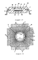
- heater member (heater insert) 38 provided with linear concave parts (grooves) 52 arranged radially and square-shaped concave part 51 for inserting support pins 32 and mounting pad 31 is prepared.
- concave parts 51 and 52 are indicated with slanted lines.
- the IC chip back surface contacts heater member 38 as shown in Figure 8.
- the tip area of inner lead (7) is provided with gradation 39 of heater member front surface so definite contact is made with the heater member when pressurized by inner lead clamp 70 (see Figure 6), contact which is thermally and mechanically stable is secured as noted above, and stabilized bonding is executed.
- Wire bonding is executed by bonding wire 15 to pad 17 with capillary 19 by applying thermal or ultrasonic energy, guiding it to insert lead 7 like arrow 20, then cladding it in the same manner as noted earlier.
- mounting pad 31 is formed to be smaller as noted above, it is supported by heater insert 38 sufficiently so wire bonding can be executed stably, and moreover, the heat from the heater can be conducted directly to IC chip 10 from heater insert 38 so thermal efficiency is not lost.
- mounting pad 31 is formed to be smaller than IC chip 10 and silver paste 34 fills in concave part 30 so the following functional effects (1)-(5) can be obtained.
- the manufacturing method of packages according to this embodiment uses heater insert 38 provided with mounting pad insertion concave part 51 and executes bonding by directly supporting IC chip 10 at the periphery so the following functional effects (6)-(7) are manifested.
- a package that had been set (cured) after resin-sealing was shelved for a prescribed period of time (refer to TABLE I below) at 85°C/85% RH. Thereafter, it was placed on a printed wiring board then passed through an IR reflow furnace (maximum temperature 245°C/5 sec) once. Thereafter, the cracks on the inside of the resin were observed with an ultrasonic detector.
- a package that was set (cured) after resin-sealing was subjected to moisture absorption for 168 h at 85°C/30% RH. Thereafter, it was passed through an IR reflow furnace (maximum temperature 245°C/5 sec) three times. Thereafter, a temperature cycle test (160°C/-66°C, as the timing, held for 10 min at each temperature) was executed in prescribed frequency. Thereafter, cracks on the inside part of the resin were observed with an ultrasonic detector as above and by external inspection.
- the curvature of the package was measured. Namely, with the depth at the back surface (the surface on the bottom side of the IC chip 10 in Figure 1, for example) of the center position of the package shown in Figure 1 as 0, the depth at the four corner positions of the package was measured (the thickness of the package was 1.4 mm, the IC chip size was 8.1 mm x 8.3 mm, and the IC chip thickness was 0.28 mm).
- the curvature on the package front surface side was expressed with negative depth and curvature on the back surface side was expressed with positive depth, and the average value of the measured depth at the four corners was evaluated as the "curvature of the package.” The results are shown in Table III (however, the unit of depth is ⁇ m).
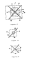
- FIGS 9-18 show other embodiments of the present invention.
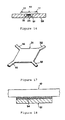
- side surface 60 at the four sides of the mounting pad 31 is slanted inwardly, for example, linearly from chip mounting surface (front side) towards the opposite surface (back surface). In conformance therewith, even the side surface of the concave part 51 receiving heater insert 38 shown in Figure 6 is slanted.
- the insertion of heater insert 38 into the concave part 51 is made easy and the inserted state of the heater insert 38 after the insertion is further stabilized. Also, it is possible to disperse the stress generated between mounting pad 31 and resin 16 by the heat applied during the IR reflow shown in Figure 10 along slanted surface 60, and to relax the concentration of stress compared to when edge 31a of pad 31 is at a right angle, thereby preventing cracks in the resin 16 even more effectively.
- the slanted shape of the side surface 60 is not limited to a linear shape but can be other shapes such as a curved shape, etc.
- Figures 11(a) and 11(b) illustrates the slanted side surface 61 of the support pin 32, for example, as a curved shape from the IC chip mounting side (surface side) inwardly towards the opposite side (back side).
- insertion of the support pin 32 becomes simple as indicated in Figures 11 (a) and 11(b) when placing the lead frame into heater insert 38 and the inserted state of the support pin 32 is further stabilized.
- the support pin 32 is even more effective when combined with a mounting pad 31 having a slanted surface 60 as shown in Figure 9.
- the slanted shape of the side surface 61 of the support pin 32 is not limited to a curved shape and can be other shapes such as a linear shape, etc.
- the adhesive strength of IC chip 10 on the lead frame is improved by providing an additional mounting part 62 of a circular shape on the support pin 32 and fixing IC chip 10 even on the mounting part 62 when the adhesive strength of the IC chip 10 as secured with respect to mounting pad 31 is insufficient.
- the mounting part 62 is not limited to circular shape and can be of various shapes such as triangular, square, other polygonal shapes, or elliptic shapes.
- a circular shaped mounting part insertion concave part 64 is also formed on heater insert 38 as in shown Figure 13.
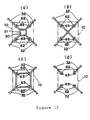
- Figure 14 shows an example of providing two support pins 32 on the diagonal line of mounting pad 31, whereas the previously described examples are provided with support pins 32 at the four corners (a total of four support pins 32) of mounting pad 31.
- mounting pad 31 can be sufficiently supported. Furthermore, there may be three support pins 32 by providing them at the three corner parts of mounting pad 31.
- the example in Figure 15 makes the shape of mounting pad 31 into another shape other than the square shape noted above, for example, a round or near round shape.
- the pad shape With a round pad shape, it is possible to disperse the stress between the resin and the mounting pad, to relax the stress concentration, and to improve the crack resistance.
- the pad shape can be various shapes such as polygonal shape, curved shape, etc.
- mounting pad insertion concave part 51 of the heater insert 38 used for wire bonding is made larger than the mounting pad 31 so that the mounting pad 31 may be inserted into concave part 51 with a margin.
- Figures 17 and 18 differ from the previous examples in that a concave part for receiving the silver paste filling is not formed in mounting pad 31.
- the lead frame material can be a metal such as a 42 alloy, copper alloy, copper, etc.
- the fixing agent can be an adhesive other than silver paste
- the heater insert can be stainless steel, etc.
- a configuration similar to the lead frame can be applied in other types of lead frames, for example, a tape carrier type.
- the bonding is also not limited to wire bonding.
- the present invention can be applied to dual in-line packages, etc., and is not limited to a QFP package in which the terminals (leads) are output in four directions.
- the present invention involves making the mounting part of the mounting pad, etc., smaller than the semiconductor element so the warpage of the semiconductor element created by differences in the thermal expansion and contraction of the mounting part and the resin is minimized, and the generation of curvature is also reduced. Moreover, due to the adhesion of the resin with respect to the semiconductor element being very favorable and due to an increase in the adhesion area, the adhesive strength between the resin and semiconductor element does not decrease in the vicinity of the mounting part, separation of the mounting part and the resin due to the condensation of moisture causing vapor explosion is eliminated, and cracks are not created in the resin, or at least the number of cracks are reduced considerably.
- the mounting part is small so the size of the semiconductor element which can be mounted on it is not dependent on the size of the mounting part and the freedom in the semiconductor element size which can be mounted is increased.
- the semiconductor element directly contacts the heater insert so that heat conduction and ultrasonic energy to the semiconductor element from the heater are not lost.
- the bonding strength is maintained favorably and even if the heat of the heater and energy needed for the cladding are made low, sufficient bonding can be executed.
Landscapes
- Die Bonding (AREA)
- Lead Frames For Integrated Circuits (AREA)
- Encapsulation Of And Coatings For Semiconductor Or Solid State Devices (AREA)
- Wire Bonding (AREA)
Applications Claiming Priority (3)
| Application Number | Priority Date | Filing Date | Title |
|---|---|---|---|
| JP165248/93 | 1993-06-10 | ||
| JP16524893A JP3281994B2 (ja) | 1993-06-10 | 1993-06-10 | 樹脂封止型半導体装置 |
| JP16524893 | 1993-06-10 |
Publications (3)
| Publication Number | Publication Date |
|---|---|
| EP0628997A2 true EP0628997A2 (de) | 1994-12-14 |
| EP0628997A3 EP0628997A3 (de) | 1995-09-06 |
| EP0628997B1 EP0628997B1 (de) | 2002-04-10 |
Family
ID=15808699
Family Applications (1)
| Application Number | Title | Priority Date | Filing Date |
|---|---|---|---|
| EP94304221A Expired - Lifetime EP0628997B1 (de) | 1993-06-10 | 1994-06-10 | Halbleiteranordnung mit schmallem Träger und Herstellungsverfahren |
Country Status (7)
| Country | Link |
|---|---|
| US (1) | US5623123A (de) |
| EP (1) | EP0628997B1 (de) |
| JP (1) | JP3281994B2 (de) |
| KR (1) | KR100331666B1 (de) |
| DE (1) | DE69430341T2 (de) |
| MY (1) | MY121890A (de) |
| SG (1) | SG48840A1 (de) |
Cited By (6)
| Publication number | Priority date | Publication date | Assignee | Title |
|---|---|---|---|---|
| EP0849794A1 (de) * | 1996-12-20 | 1998-06-24 | Texas Instruments Incorporated | Leiterrahmen mit feinem Kontaktabstand |
| WO1999000826A2 (en) | 1997-06-27 | 1999-01-07 | Matsushita Electronics Corporation | Resin molded type semiconductor device and a method of manufacturing the same |
| EP0862211A3 (de) * | 1997-02-27 | 2000-11-08 | Oki Electric Industry Co., Ltd. | Halbleiteranordnung und Herstellungsverfahren dafür |
| DE10111028A1 (de) * | 2001-03-07 | 2002-09-19 | Infineon Technologies Ag | Chipkartenmodul |
| EP1302983A1 (de) * | 2001-10-15 | 2003-04-16 | Siliconix (Taiwan) Ltd. | Leiterrahmen mit mit Nuten versehenen Träger |
| US7538416B2 (en) | 1997-06-27 | 2009-05-26 | Panasonic Corporation | Resin molded type semiconductor device and a method of manufacturing the same |
Families Citing this family (34)
| Publication number | Priority date | Publication date | Assignee | Title |
|---|---|---|---|---|
| JPH09153586A (ja) * | 1995-12-01 | 1997-06-10 | Texas Instr Japan Ltd | 半導体装置、その製造方法、及びリードフレーム |
| KR980006164A (ko) * | 1996-06-20 | 1998-03-30 | 황인길 | 패키지와의 몰딩성을 증대시킨 반도체패키지의 리드프레임 탑재판 |
| JP2904141B2 (ja) * | 1996-08-20 | 1999-06-14 | 日本電気株式会社 | 半導体装置 |
| JP3535328B2 (ja) * | 1996-11-13 | 2004-06-07 | 株式会社ルネサステクノロジ | リードフレームとこれを用いた半導体装置 |
| JPH113953A (ja) * | 1997-06-10 | 1999-01-06 | Fujitsu Ltd | 半導体装置の製造方法及び半導体装置 |
| US6157074A (en) * | 1997-07-16 | 2000-12-05 | Hyundai Electronics Industries Co., Ltd. | Lead frame adapted for variable sized devices, semiconductor package with such lead frame and method for using same |
| WO1999023700A1 (en) | 1997-11-05 | 1999-05-14 | Martin Robert A | Chip housing, methods of making same and methods for mounting chips therein |
| US6404067B1 (en) | 1998-06-01 | 2002-06-11 | Intel Corporation | Plastic ball grid array package with improved moisture resistance |
| US6175487B1 (en) | 1998-08-15 | 2001-01-16 | Nsi Enterprises, Inc. | Luminaire assembly |
| JP2000124235A (ja) | 1998-10-16 | 2000-04-28 | Oki Electric Ind Co Ltd | 樹脂封止半導体装置 |
| US6545342B1 (en) * | 1999-05-03 | 2003-04-08 | Texas Instruments Incorporated | Pre-finished leadframe for semiconductor devices and method of fabrication |
| JP2001024132A (ja) * | 1999-06-30 | 2001-01-26 | Texas Instr Inc <Ti> | 半導体デバイス用変形吸収形リードフレーム |
| JP2001244292A (ja) * | 2000-03-01 | 2001-09-07 | Mitsubishi Electric Corp | 半導体装置のワイヤボンデイング装置およびワイヤボンデイング方法 |
| US6372539B1 (en) | 2000-03-20 | 2002-04-16 | National Semiconductor Corporation | Leadless packaging process using a conductive substrate |
| US6452255B1 (en) * | 2000-03-20 | 2002-09-17 | National Semiconductor, Corp. | Low inductance leadless package |
| US6686652B1 (en) | 2000-03-20 | 2004-02-03 | National Semiconductor | Locking lead tips and die attach pad for a leadless package apparatus and method |
| US6399415B1 (en) | 2000-03-20 | 2002-06-04 | National Semiconductor Corporation | Electrical isolation in panels of leadless IC packages |
| US20030137032A1 (en) * | 2000-05-01 | 2003-07-24 | Abbott Donald C. | Pre-finished leadframe for semiconductor devices and method fo fabrication |
| TW434856B (en) * | 2000-05-15 | 2001-05-16 | Siliconware Precision Industries Co Ltd | Manufacturing method for high coplanarity solder ball array of ball grid array integrated circuit package |
| US6828663B2 (en) * | 2001-03-07 | 2004-12-07 | Teledyne Technologies Incorporated | Method of packaging a device with a lead frame, and an apparatus formed therefrom |
| JP2002299540A (ja) * | 2001-04-04 | 2002-10-11 | Hitachi Ltd | 半導体装置およびその製造方法 |
| TW568355U (en) * | 2002-01-16 | 2003-12-21 | Orient Semiconductor Elect Ltd | Improved leadframe structure for integrated circuit |
| US6885093B2 (en) * | 2002-02-28 | 2005-04-26 | Freescale Semiconductor, Inc. | Stacked die semiconductor device |
| JP4073308B2 (ja) * | 2002-12-20 | 2008-04-09 | 三洋電機株式会社 | 回路装置の製造方法 |
| JP2005327830A (ja) * | 2004-05-13 | 2005-11-24 | Mitsubishi Electric Corp | 半導体マイクロデバイス |
| JP2008085002A (ja) * | 2006-09-27 | 2008-04-10 | Sanyo Electric Co Ltd | 半導体装置およびその製造方法 |
| US7656236B2 (en) * | 2007-05-15 | 2010-02-02 | Teledyne Wireless, Llc | Noise canceling technique for frequency synthesizer |
| US8179045B2 (en) * | 2008-04-22 | 2012-05-15 | Teledyne Wireless, Llc | Slow wave structure having offset projections comprised of a metal-dielectric composite stack |
| JP5101538B2 (ja) * | 2009-01-30 | 2012-12-19 | 京セラクリスタルデバイス株式会社 | 圧電発振器 |
| US9274140B2 (en) * | 2013-02-20 | 2016-03-01 | Silicon Laboratories Inc. | Multi-purpose integrated circuit device contactor |
| US9202660B2 (en) | 2013-03-13 | 2015-12-01 | Teledyne Wireless, Llc | Asymmetrical slow wave structures to eliminate backward wave oscillations in wideband traveling wave tubes |
| KR20240018908A (ko) * | 2022-08-03 | 2024-02-14 | 삼성전자주식회사 | 솔더 리플로우 장치 및 이를 이용한 전자 장치의 제조 방법 |
| KR20240018915A (ko) | 2022-08-03 | 2024-02-14 | 삼성전자주식회사 | 솔더 리플로우 장치 및 이를 이용한 전자 장치의 제조 방법 |
| CN118471867B (zh) * | 2024-07-13 | 2024-09-24 | 中北大学 | 一种半导体封装测试装置及其测试方法 |
Family Cites Families (14)
| Publication number | Priority date | Publication date | Assignee | Title |
|---|---|---|---|---|
| JPS5867035A (ja) * | 1981-10-19 | 1983-04-21 | Toshiba Corp | 半導体装置の製造方法 |
| JPS5992535A (ja) * | 1982-11-18 | 1984-05-28 | Toshiba Corp | 半導体装置 |
| JPS6072236A (ja) * | 1983-09-28 | 1985-04-24 | Toshiba Corp | 半導体装置 |
| JPS6269628A (ja) * | 1985-09-24 | 1987-03-30 | Toshiba Corp | 半導体装置とその製造方法 |
| US4857989A (en) * | 1986-09-04 | 1989-08-15 | Mitsubishi Denki Kabushiki Kaisha | Semiconductor device |
| JPS63216365A (ja) * | 1987-03-05 | 1988-09-08 | Tomoegawa Paper Co Ltd | 半導体装置 |
| JPS63308359A (ja) * | 1987-06-10 | 1988-12-15 | Mitsui Haitetsuku:Kk | リ−ドフレ−ムの製造方法 |
| JPH01187841A (ja) * | 1988-01-22 | 1989-07-27 | Hitachi Ltd | 半導体装置 |
| JPH0332048A (ja) * | 1989-06-29 | 1991-02-12 | Seiko Epson Corp | 半導体装置 |
| US5237205A (en) * | 1989-10-02 | 1993-08-17 | Advanced Micro Devices, Inc. | Ground plane for plastic encapsulated integrated circuit die packages |
| JPH04171751A (ja) * | 1990-11-05 | 1992-06-18 | Nec Corp | 半導体装置のリードフレーム |
| JPH04258156A (ja) * | 1991-02-13 | 1992-09-14 | Sharp Corp | 半導体装置 |
| JPH04280439A (ja) * | 1991-03-08 | 1992-10-06 | Fujitsu Ltd | 半導体装置およびその製造方法 |
| JP2509422B2 (ja) * | 1991-10-30 | 1996-06-19 | 三菱電機株式会社 | 半導体装置及びその製造方法 |
-
1993
- 1993-06-10 JP JP16524893A patent/JP3281994B2/ja not_active Expired - Fee Related
-
1994
- 1994-06-09 MY MYPI94001472A patent/MY121890A/en unknown
- 1994-06-10 DE DE69430341T patent/DE69430341T2/de not_active Expired - Fee Related
- 1994-06-10 SG SG1996002657A patent/SG48840A1/en unknown
- 1994-06-10 KR KR1019940013095A patent/KR100331666B1/ko not_active Expired - Fee Related
- 1994-06-10 EP EP94304221A patent/EP0628997B1/de not_active Expired - Lifetime
- 1994-06-10 US US08/258,119 patent/US5623123A/en not_active Expired - Lifetime
Cited By (8)
| Publication number | Priority date | Publication date | Assignee | Title |
|---|---|---|---|---|
| EP0849794A1 (de) * | 1996-12-20 | 1998-06-24 | Texas Instruments Incorporated | Leiterrahmen mit feinem Kontaktabstand |
| EP0862211A3 (de) * | 1997-02-27 | 2000-11-08 | Oki Electric Industry Co., Ltd. | Halbleiteranordnung und Herstellungsverfahren dafür |
| EP1528595A1 (de) * | 1997-02-27 | 2005-05-04 | Oki Electric Industry Co., Ltd. | Leiterrahmen, Drahtverbindungsvorrichtung und Herstellungsverfahren einer Halbleiteranordnung |
| WO1999000826A2 (en) | 1997-06-27 | 1999-01-07 | Matsushita Electronics Corporation | Resin molded type semiconductor device and a method of manufacturing the same |
| US7538416B2 (en) | 1997-06-27 | 2009-05-26 | Panasonic Corporation | Resin molded type semiconductor device and a method of manufacturing the same |
| EP0996962B1 (de) * | 1997-06-27 | 2010-08-18 | Panasonic Corporation | In harz gegossene halbleiteranordnung |
| DE10111028A1 (de) * | 2001-03-07 | 2002-09-19 | Infineon Technologies Ag | Chipkartenmodul |
| EP1302983A1 (de) * | 2001-10-15 | 2003-04-16 | Siliconix (Taiwan) Ltd. | Leiterrahmen mit mit Nuten versehenen Träger |
Also Published As
| Publication number | Publication date |
|---|---|
| SG48840A1 (en) | 1998-05-18 |
| EP0628997B1 (de) | 2002-04-10 |
| JP3281994B2 (ja) | 2002-05-13 |
| DE69430341T2 (de) | 2002-10-02 |
| EP0628997A3 (de) | 1995-09-06 |
| KR950001998A (ko) | 1995-01-04 |
| DE69430341D1 (de) | 2002-05-16 |
| KR100331666B1 (ko) | 2002-08-14 |
| MY121890A (en) | 2006-03-31 |
| US5623123A (en) | 1997-04-22 |
| JPH06350010A (ja) | 1994-12-22 |
Similar Documents
| Publication | Publication Date | Title |
|---|---|---|
| EP0628997B1 (de) | Halbleiteranordnung mit schmallem Träger und Herstellungsverfahren | |
| KR930007370B1 (ko) | 전자 장치 및 이에 사용되는 리이드 프레임 | |
| US4942452A (en) | Lead frame and semiconductor device | |
| JP2891607B2 (ja) | 半導体集積回路装置の製造方法 | |
| US5960260A (en) | Semiconductor device, its manufacturing method, and dicing adhesive element therefor | |
| JPH09153586A (ja) | 半導体装置、その製造方法、及びリードフレーム | |
| JPH04264758A (ja) | 半導体チップキャリア | |
| JPH10199912A (ja) | 半導体装置 | |
| KR0148080B1 (ko) | 반도체 리드프레임 제조방법 및 그를 이용한 반도체 칩 패키지 제조방법 | |
| JPS60167454A (ja) | 半導体装置 | |
| JPH10242368A (ja) | 半導体装置およびその製造方法ならびに半導体モジュールおよびicカード | |
| JPH11102928A (ja) | Csp型半導体装置及びその製造方法 | |
| JPH11150213A (ja) | 半導体装置 | |
| US20070290303A1 (en) | Dual leadframe semiconductor device package | |
| JP3129169B2 (ja) | 半導体装置及びその製造方法 | |
| JP2000003981A (ja) | 半導体装置およびその製造方法 | |
| JPH07161910A (ja) | 樹脂封止型半導体装置 | |
| JP2000012756A (ja) | 半導体装置およびその製造方法並びにそれを使用した実装構造体 | |
| JPH0870082A (ja) | 半導体集積回路装置およびその製造方法ならびにリードフレーム | |
| JPH08204048A (ja) | 半導体チップの封止構造 | |
| JPH09330962A (ja) | 半導体集積回路装置およびその製造方法 | |
| JPH0855856A (ja) | 半導体装置とその製造方法 | |
| JPH1197586A (ja) | 半導体装置およびその製造方法 | |
| JPH0637221A (ja) | 樹脂封止型半導体装置 | |
| JPH1012797A (ja) | リードフレーム及びそのリードフレームを用いた樹脂封止型半導体装置及びその製造方法 |
Legal Events
| Date | Code | Title | Description |
|---|---|---|---|
| PUAI | Public reference made under article 153(3) epc to a published international application that has entered the european phase |
Free format text: ORIGINAL CODE: 0009012 |
|
| AK | Designated contracting states |
Kind code of ref document: A2 Designated state(s): DE FR GB NL |
|
| PUAL | Search report despatched |
Free format text: ORIGINAL CODE: 0009013 |
|
| AK | Designated contracting states |
Kind code of ref document: A3 Designated state(s): DE FR GB NL |
|
| 17P | Request for examination filed |
Effective date: 19960304 |
|
| 17Q | First examination report despatched |
Effective date: 19981222 |
|
| GRAG | Despatch of communication of intention to grant |
Free format text: ORIGINAL CODE: EPIDOS AGRA |
|
| GRAG | Despatch of communication of intention to grant |
Free format text: ORIGINAL CODE: EPIDOS AGRA |
|
| GRAH | Despatch of communication of intention to grant a patent |
Free format text: ORIGINAL CODE: EPIDOS IGRA |
|
| GRAH | Despatch of communication of intention to grant a patent |
Free format text: ORIGINAL CODE: EPIDOS IGRA |
|
| REG | Reference to a national code |
Ref country code: GB Ref legal event code: IF02 |
|
| GRAA | (expected) grant |
Free format text: ORIGINAL CODE: 0009210 |
|
| AK | Designated contracting states |
Kind code of ref document: B1 Designated state(s): DE FR GB NL |
|
| PG25 | Lapsed in a contracting state [announced via postgrant information from national office to epo] |
Ref country code: NL Free format text: LAPSE BECAUSE OF FAILURE TO SUBMIT A TRANSLATION OF THE DESCRIPTION OR TO PAY THE FEE WITHIN THE PRESCRIBED TIME-LIMIT Effective date: 20020410 |
|
| REF | Corresponds to: |
Ref document number: 69430341 Country of ref document: DE Date of ref document: 20020516 |
|
| ET | Fr: translation filed | ||
| NLV1 | Nl: lapsed or annulled due to failure to fulfill the requirements of art. 29p and 29m of the patents act | ||
| PLBE | No opposition filed within time limit |
Free format text: ORIGINAL CODE: 0009261 |
|
| STAA | Information on the status of an ep patent application or granted ep patent |
Free format text: STATUS: NO OPPOSITION FILED WITHIN TIME LIMIT |
|
| 26N | No opposition filed |
Effective date: 20030113 |
|
| PGFP | Annual fee paid to national office [announced via postgrant information from national office to epo] |
Ref country code: FR Payment date: 20090605 Year of fee payment: 16 |
|
| PGFP | Annual fee paid to national office [announced via postgrant information from national office to epo] |
Ref country code: DE Payment date: 20090630 Year of fee payment: 16 |
|
| PGFP | Annual fee paid to national office [announced via postgrant information from national office to epo] |
Ref country code: GB Payment date: 20100401 Year of fee payment: 17 |
|
| REG | Reference to a national code |
Ref country code: FR Ref legal event code: ST Effective date: 20110228 |
|
| PG25 | Lapsed in a contracting state [announced via postgrant information from national office to epo] |
Ref country code: DE Free format text: LAPSE BECAUSE OF NON-PAYMENT OF DUE FEES Effective date: 20110101 |
|
| PG25 | Lapsed in a contracting state [announced via postgrant information from national office to epo] |
Ref country code: FR Free format text: LAPSE BECAUSE OF NON-PAYMENT OF DUE FEES Effective date: 20100630 |
|
| GBPC | Gb: european patent ceased through non-payment of renewal fee |
Effective date: 20110610 |
|
| PG25 | Lapsed in a contracting state [announced via postgrant information from national office to epo] |
Ref country code: GB Free format text: LAPSE BECAUSE OF NON-PAYMENT OF DUE FEES Effective date: 20110610 |