EP0578307B1 - Chip carrier with protective coating for circuitized surface - Google Patents
Chip carrier with protective coating for circuitized surface Download PDFInfo
- Publication number
- EP0578307B1 EP0578307B1 EP93201907A EP93201907A EP0578307B1 EP 0578307 B1 EP0578307 B1 EP 0578307B1 EP 93201907 A EP93201907 A EP 93201907A EP 93201907 A EP93201907 A EP 93201907A EP 0578307 B1 EP0578307 B1 EP 0578307B1
- Authority
- EP
- European Patent Office
- Prior art keywords
- encapsulant
- chip carrier
- composition
- chip
- coating
- Prior art date
- Legal status (The legal status is an assumption and is not a legal conclusion. Google has not performed a legal analysis and makes no representation as to the accuracy of the status listed.)
- Expired - Lifetime
Links
Images
Classifications
-
- H10W74/121—
-
- H10W72/071—
-
- H10W74/012—
-
- H10W74/15—
-
- H10W74/47—
-
- H10W72/07251—
-
- H10W72/20—
-
- H10W72/856—
-
- H10W72/877—
-
- H10W90/724—
-
- H10W90/734—
-
- H10W90/736—
-
- Y—GENERAL TAGGING OF NEW TECHNOLOGICAL DEVELOPMENTS; GENERAL TAGGING OF CROSS-SECTIONAL TECHNOLOGIES SPANNING OVER SEVERAL SECTIONS OF THE IPC; TECHNICAL SUBJECTS COVERED BY FORMER USPC CROSS-REFERENCE ART COLLECTIONS [XRACs] AND DIGESTS
- Y10—TECHNICAL SUBJECTS COVERED BY FORMER USPC
- Y10S—TECHNICAL SUBJECTS COVERED BY FORMER USPC CROSS-REFERENCE ART COLLECTIONS [XRACs] AND DIGESTS
- Y10S428/00—Stock material or miscellaneous articles
- Y10S428/901—Printed circuit
Definitions
- the invention pertains generally to chip carriers, and more particularly to a chip carrier having a circuitized surface which is at least partially covered by a protective, ultraviolet (UV) radiation cured coating.
- UV ultraviolet
- One type of semiconductor chip package includes one or more semiconductor chips mounted on a circuitized surface of a substrate, e.g., a ceramic substrate or a plastic substrate.
- a semiconductor chip package conventionally termed a chip carrier, is usually intended for mounting on a printed circuit card or printed circuit board. If, for example, surface mounting is to be used, then the chip carrier will conventionally include a lead frame or edge clip which is mechanically and electrically connected to electrical contact pads formed around the periphery of the chip-bearing, circuitized surface of the substrate.
- a relatively high density of chip connections is readily achieved by mounting one or more semiconductor chips on the circuitized surface of a chip carrier substrate in the so-called flip chip configuration.
- the chip or chips are mounted face-down on solderable metal pads on the substrate using solder balls.
- the coefficient of thermal expansion (CTE) of, for example, a silicon chip is significantly different from the CTE of a ceramic substrate or plastic substrate.
- encapsulant having a CTE which is within 30 percent of the CTE of the solder balls.
- Useful such encapsulants have a composition which includes, for example, an epoxy binder, e.g. a cycloaliphatic epoxide binder, and a filler, e.g. high purity fused or amorphous silica, as disclosed in US-A-4,999,699.
- the binder should have a viscosity at room temperature which is no greater than about 1000 centipoise and the filler should have a maximum particle size which is no greater than 31 microns.
- the binder should constitute about 60 to about 25 percent by weight of the total of binder and filler, while the filler should constitute about 40 to about 75 percent by weight of the total.
- One technique for achieving such protection is to mount a ceramic cap over the chip or chips and at least a portion of the circuitry on the circuitized surface. While the use of such a ceramic cap for achieving mechanical and environmental protection is effective, its use significantly increases the cost of the chip carrier. Moreover, the presence of the ceramic cap precludes the possibility of directly mounting a heat sink on the chip or chips in order to dissipate the heat produced by the chip or chips.
- the heat sink is necessarily mounted on the ceramic cap, and a thermal grease must then be provided between the upper surface of each chip and the ceramic cap to achieve good thermal contact between the chip or chips and the heat sink. While this procedure is effective for dissipating heat, it would be more convenient if the heat sink could be directly mounted on the chip or chips.
- circuitry on the circuitized surface of a chip carrier substrate be covered by a coating having a composition which includes an epoxy binder and a filler, in order to provide mechanical and environmental protection for the circuitry at a relatively low cost.
- a coating having a composition which includes an epoxy binder and a filler in order to provide mechanical and environmental protection for the circuitry at a relatively low cost.
- Such filled epoxy coatings have been applied to the upper (non-circuit bearing) surfaces of chips and have proven to be useful.
- protective coatings for the circuitry on the circuitized surfaces of chip carriers which are: (1) relatively inexpensive; (2) capable of withstanding standard thermal cycling tests without cracking and without delaminating to provide effective mechanical and environmental protection for the circuitry; (3) hydrophobic; (4) exhibit a low centration of ions, exemplified by the concentration of chloride ions being less than ten parts per million; (5) relatively quickly and therefore conveniently cured;and (6) permit heat sinks to be directly mounted on chips.
- EP-A-340492 concerns a chip carrier, according to the precharacterising part of claim 1 and EP-A-335019 concerns a further chip carrier.
- the invention as set out in claim 1 involves the finding that the epoxy coatings previously proposed as protective coatings for the circuitry on the circuitized surfaces of chip carriers all had relatively high moduli of elasticity, i.e., moduli of elasticity greater than about 69.10 6 N/m 2 (10,000 psi), at room temperature (25 °C). As a consequence, these coatings lacked the flexibility needed to withstand the stresses associated with the thermal cycling tests, described above, which led to cracking and delamination.
- compositions which include appropriately chosen, and appropriate relative amounts of, acrylated urethane oligomer, acrylated monomer and photoinitiator are relatively quickly cured, e.g., cured within 5 seconds, using UV radiation to yield relatively inexpensive, hydrophobic coatings having moduli of elasticity equal to or less than about 69.10 6 N/m 2 at room temperature.
- these coatings readily withstand thermal cycling tests without cracking or delaminating.
- these coatings exhibit chloride ion concentrations less than ten parts per million, and therefore do not cause ion- induced corrosion and migration.
- heat sinks are readily directly mounted on the chips.
- the invention involves a chip carrier including a chip carrier substrate, e.g., a ceramic substrate or a plastic substrate, having a circuitized surface on which is mounted at least one semiconductor chip in a flip chip configuration.
- the solder ball connections between the at least one semiconductor chip and the chip carrier substrate are encapsulated in an encapsulant having a composition which includes, for example, an epoxy, and having a CTE which is within 30 percent of the CTE of the solder balls.
- a protective, relatively inexpensive coating having a 69.10 6 N/m 2 composition which is chosen, in accordance with the invention, so that this coating: (1) readily withstands the thermal cycling tests, described above, without exhibiting any internal cracks or interfacial cracks at the coating/solder ball encapsulant interface, and without delaminating, when viewed under a 10x optical microscope; (2) is hydrophobic; (3) exhibits a chloride ion concentration less than ten parts per million; (4) is relatively quickly and conveniently cured using UV radiation; and (5) permits heat sinks to be directly mounted onto chips.
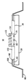
- a preferred embodiment of a chip carrier 10 includes a substrate 20, e.g., a ceramic substrate, such as an alumina substrate, or a plastic substrate.
- This substrate 20 has a circuitized surface 30, including circuit lines (not shown) and electrical contact pads 40 of, for example, copper.
- At least one semiconductor chip 50 e.g., a silicon chip, is mounted in a flip chip configuration on the circuitized surface 30 using solder balls 60 having a composition which includes, for example, three percent (by weight) tin and ninety seven percent (by weight) lead.
- the solder balls 60 are encapsulated in an encapsulant 70 having a CTE which is within 30 percent of the CTE of the solder balls 60.
- the composition of the solder ball encapsulant 70 includes, for example, an epoxy binder, e.g., a cycloaliphatic polyepoxide binder, and a filler, e.g., high purity fused or amorphous silica, as disclosed in US-A-4,999,699.
- the chip carrier 10 also includes a metallic lead frame or edge clip 80 of, for example, copper, which is mechanically and electrically connected to the contact pads 40.
- a metallic lead frame or edge clip 80 of, for example, copper, which is mechanically and electrically connected to the contact pads 40.
- each of the mechanical/electrical connections between the lead frame or edge clip 80 and the contact pads 40 includes a region of solder 90, having a composition which includes, for example, ten percent (by weight) tin and ninety percent (by weight) lead.
- each solder connection between a contact pad 40 and the lead frame or edge clip 80 is at least partially, and preferably totally, encapsulated in a region of material 100.
- the composition of the material region 100 is chosen so that after the combination of the solder region 90 and material region 100 is subjected to sinusoidal thermal cycling between 0 °C and 100 °C, at a frequency of three cycles per hour, for at least 2,000 cycles, the solder region 90 exhibits an increase in electrical resistance less than 200 milliohms.
- a material region 100 comprised of an at least partially filled epoxy resin having a CTE which is within +/- 30 percent of the CTE of the solder region 90.
- One such useful epoxy resin is a cyclohexyldiepoxide resin partially filled with silica filler material, which is sold under the trade name Hysol FP0045 by the Dexter Corporation of California, U.S.A.
- a coating 110 which serves to protect the covered circuitry from mechanical and environmental hazards.
- This coating 110 also contacts, and at least partially encircles, the encapsulant 70 encapsulating the solder balls 60.
- the composition used to form the coating 110 is dispensed onto the circuitized surface 30 using a syringe, and readily flows over this surface to cover exposed circuitry after being dispensed.
- the composition dispensed to form the coating 110 includes three components: (1) an acrylated urethane oligomer; (2) an acrylated monomer; and (3) a photoinitiator.
- the presence of the acrylated urethane oligomer tends, among other things, to make the corresponding coating 110 hydrophobic.
- the acrylated monomer serves as a diluent for the acrylated urethane oligomer and undergoes cross-linking to the latter when the dispensed composition is subjected to UV radiation.
- the presence of the photoinitiator makes such cross-linking possible under the influence of the UV radiation.
- a variety of acrylated urethane oligomers, acrylated monomers and photoinitiators are useful in the invention. In this regard, it has been found that it is primarily the combination of oligomer and monomer which determines the elasticity of the corresponding coating 110. It has also been found that useful elasticity-producing combinations of acrylated urethane oligomer and acrylated monomer are readily found empirically by forming compositions from such oligomers and monomers (and photoinitiators), curing these compositions using UV radiation and then measuring the modulus of elasticity of the resulting coating 110 at room temperature using, for example, a conventional tensile test. If the measured modulus is equal to or less than about 69.10 6 N/m 2 , then the corresponding combination of oligomer and monomer is useful in the invention, at least in so far as to yield a coating 110 having useful elastic properties.
- oligomer, monomer and photoinitiator which determines the concentration of chloride ions in the resulting coating 110, and therefore the degree of ion-induced corrosion and migration.
- useful combinations of oligomer, monomer and photoinitiator are readily empirically found by forming corresponding compositions on circuitized surfaces of chip carriers, curing these compositions using UV radiation and then measuring the ability of the resulting coating to prevent corrosion. That is, the corrosion behavior is ascertained by exposing the coating-covered circuitized surface to an air environment at 85°C, at 80 percent relative humidity, for 1,000 hours. An increase in the DC electrical resistance of any circuit line of 100 percent or more is an indication of significant corrosion activity and is considered unacceptable, for purposes of the present invention.
- the migration behavior is ascertained by exposing the coating -covered circuitized surface to an air environment at 85°C, at 80 percent relative humidity, under the continuous influence of a ten volt bias, for 1,000 hours.
- a DC electrical resistance between any two adjacent circuit lines less than ten megohms is an indication of significant migration behavior and is considered unacceptable, for purposes of the present invention.
- a photoinitiator In addition to the requirements on ion-induced corrosion and migration, a photoinitiator, to be useful in the present invention, must enable the useful acrylated urethane oligomers to undergo essentially complete cross-linking with the useful acrylated monomers under the influence of UV radiation, at the intensities and over the time periods discussed below.
- Such useful photoinitiators are readily found empirically by initially adding a photoinitiator to a composition which includes a useful acrylated urethane oligomer and a useful acrylated monomer, and subjecting the resulting composition to UV radiation having the intensities, and for the durations, specified below, to produce a first coating sample.
- first coating sample which is a measure of the degree of cross-linking
- second such coating sample is then produced by subjecting another composition, including the same oligomer, monomer and photoinitiator, to the same UV radiation, at the same intensity but for a longer exposure time, or at a higher intensity but for the same exposure time.
- the measured fracture stress of the second coating sample is greater than that of the first coating sample, then this indicates that the second coating sample has undergone additional cross-linking. If, on the other hand, the fracture stress of the second coating sample is unchanged, then the first coating sample is assumed to have achieved complete, or essentially complete, cross-linking. Provided the UV intensity and exposure time needed to achieve such complete cross-linking falls within the ranges given below, then the corresponding photoinitiator is useful to the present invention. Otherwise, the photoinitiator is not useful to the present invention.
- acrylated urethane oligomers found using the above-described procedures are the acrylated urethane oligomers sold under the trade names ZL2196 and ZL1365 by Morton International, Inc., of Chicago, Illinois.
- the acrylated monomers isobornyl acrylate and 2-hydroxypropyl acrylate are useful in the invention, in combination with either ZL2196 or ZL1365 acrylated urethane oligomer.
- the following three photoinitiators are useful with any combination of the above oligomers and monomers:
- the relative amounts of the three components of the useful compositions are also important.
- the acrylated urethane oligomer should constitute about 35 percent (by weight) to about 75 percent (by weight) of a useful composition, and should preferably constitute about 65 percent (by weight) of the composition. Amounts less than about 35 percent are undesirable because the corresponding coating 110 exhibits a modulus of elasticity higher than about 69.10 6 N/m 2 and, as a consequence, exhibits internal and interfacial cracks, and delaminates, when subjected to the thermal cycling tests, described above.
- the acrylated monomer should correspondingly constitute about 63.5 percent (by weight) to about 22.5 percent (by weight) of a useful composition. Amounts outside this range are undesirable for the reasons given above.
- the photoinitiator should correspondingly constitute about 1.5 percent (by weight) to about 2.5 percent (by weight) of a useful composition. Amounts less than about 1.5 percent are undesirable because they result in insufficient cross-linking between the oligomer and the monomer. Amounts greater than about 2.5 percent are unnecessary because 2.5 percent is sufficient to achieve complete cross-linking.
- the useful compositions are readily dispensed via a syringe onto the circuitized surface 30 of the substrate 20. These compositions readily flow over the surface 30 to cover exposed circuitry and, under the influence of capillary action, readily flow up the sides of the solder ball encapsulant 70 to cover and encircle this encapsulant.
- the useful UV wavelengths include wavelength bands from 200 to 400 nanometers.
- Useful UV intensities range from about 5.5 to about 6.5 joules per square centimeter, with corresponding exposure times ranging from about 5 to about 30 seconds. UV intensities less than about 5.5 joules per square centimeter are undesirable because they result in insufficient cross-linking between the oligomer and the monomer. UV intensities greater than about 6.5 joules per square centimeter are unnecessary because complete cross-linking occurs at lower intensities and, in fact, significantly higher intensities lead to bond scission, which is counterproductive.
- a commercially available source of UV radiation capable of emitting UV radiation at the intensities and for the durations specified above is, for example, a UV curing system sold by Fusion UV Curing Systems of Rockville, Maryland, equipped with D and H lamps, as denominated by this supplier.
- the thickness of the coating 110 preferably exceeds that of the underlying, protected circuitry by about 0.5 mm. While greater coating thicknesses are useful, effective mechanical and environmental protection is readily achieved at the thickness specified above.
- the resulting coating 110 readily withstands thermal cycling from 0°C to 100°C, at a frequency of three cycles per hour, for at least 2,000 cycles without exhibiting internal or interfacial cracks, when viewed under a 10x optical microscope.
- This thermal cycling is, of course, performed in an oven having a control system which does not permit perfect adherence to the above thermal cycling specification. Rather, in practice, each complete thermal cycle has a duration of 20 +/- 2 minutes (rather than precisely 20 minutes).
- the rise time from 10°C to 90°C is 6 +3/-2 minutes
- the fall time from 90°C to 10°C is also 6 +3/-2 minutes.
- the oven reaches a peak temperature of 100 +/- 10°C, where the corresponding dwell time is 4 +/- 2 minutes. Further, the oven reaches a minimum temperature of 0 +/- 10°C, where the corresponding dwell time is also 4 +/- 2 minutes.
- the former (perfect) thermal cycling specification is to be interpreted as denoting the latter (practical) thermal cycling specification.
- a coating 110 formed in accordance with the present invention, also readily withstands the "ship shock” test, in which the coating is thermally cycled from -40°C to +65°C, at a frequency of one cycle per hour, for at least ten cycles, without delaminating from the circuitized surface 30 and without cracking, when viewed under a 10x optical microscope.
- this "ship shock” test is performed in an oven having a control system which does not permit perfect adherence to the "ship shock” thermal cycling specification. Rather, in practice, the minimum cycling temperature is -40 +/- 5°C, whereas the maximum cycling temperature is +65 +/- 5°C.
- the cycling frequency is 1 +/- 0.1 cycles per hour (rather than precisely one cycle per hour).
- the dwell time at the highest and lowest temperatures is 25 +/- 7 minutes, while the rate of increase or decrease in temperature, away from the highest and lowest temperatures, is 15°C per minute.
- the former (perfect) thermal cycling specification is to be interpreted as denoting the latter (practical) thermal cycling specification.
- a useful composition is also readily applied, via a syringe, to the upper, exposed surface of the chip 50 so that, after UV curing, a continuous coating is formed which protects both the chip 50 and the circuitized surface 30 from mechanical and environmental hazards. If, however, no coating is formed on the upper surface of the chip 50, then a heat sink 120 is readily directly mounted on the upper surface of the chip 50, as depicted in the sole accompanying drawing.
Landscapes
- Structures Or Materials For Encapsulating Or Coating Semiconductor Devices Or Solid State Devices (AREA)
- Wire Bonding (AREA)
- Epoxy Resins (AREA)
- Non-Metallic Protective Coatings For Printed Circuits (AREA)
- Die Bonding (AREA)
- Lead Frames For Integrated Circuits (AREA)
- Dicing (AREA)
- Paints Or Removers (AREA)
Applications Claiming Priority (2)
| Application Number | Priority Date | Filing Date | Title |
|---|---|---|---|
| US07/909,368 US5249101A (en) | 1992-07-06 | 1992-07-06 | Chip carrier with protective coating for circuitized surface |
| US909368 | 1992-07-06 |
Publications (3)
| Publication Number | Publication Date |
|---|---|
| EP0578307A2 EP0578307A2 (en) | 1994-01-12 |
| EP0578307A3 EP0578307A3 (en) | 1994-08-24 |
| EP0578307B1 true EP0578307B1 (en) | 1996-09-25 |
Family
ID=25427125
Family Applications (1)
| Application Number | Title | Priority Date | Filing Date |
|---|---|---|---|
| EP93201907A Expired - Lifetime EP0578307B1 (en) | 1992-07-06 | 1993-07-01 | Chip carrier with protective coating for circuitized surface |
Country Status (12)
| Country | Link |
|---|---|
| US (1) | US5249101A (env) |
| EP (1) | EP0578307B1 (env) |
| JP (1) | JP2501287B2 (env) |
| KR (1) | KR960015924B1 (env) |
| CN (1) | CN1028937C (env) |
| AT (1) | ATE143529T1 (env) |
| CA (1) | CA2091910C (env) |
| DE (1) | DE69305012T2 (env) |
| ES (1) | ES2092216T3 (env) |
| MY (1) | MY108750A (env) |
| SG (1) | SG44362A1 (env) |
| TW (1) | TW230272B (env) |
Families Citing this family (68)
| Publication number | Priority date | Publication date | Assignee | Title |
|---|---|---|---|---|
| JPH04291948A (ja) * | 1991-03-20 | 1992-10-16 | Fujitsu Ltd | 半導体装置及びその製造方法及び放熱フィン |
| JPH0538479U (ja) * | 1991-10-25 | 1993-05-25 | 曙ブレーキ工業株式会社 | ブレーキ制御機構の電磁弁装置 |
| US5288944A (en) * | 1992-02-18 | 1994-02-22 | International Business Machines, Inc. | Pinned ceramic chip carrier |
| US5390082A (en) * | 1992-07-06 | 1995-02-14 | International Business Machines, Corp. | Chip carrier with protective coating for circuitized surface |
| KR100280762B1 (ko) * | 1992-11-03 | 2001-03-02 | 비센트 비.인그라시아 | 노출 후부를 갖는 열적 강화된 반도체 장치 및 그 제조방법 |
| US5403783A (en) * | 1992-12-28 | 1995-04-04 | Hitachi, Ltd. | Integrated circuit substrate with cooling accelerator substrate |
| US5379187A (en) * | 1993-03-25 | 1995-01-03 | Vlsi Technology, Inc. | Design for encapsulation of thermally enhanced integrated circuits |
| US5539545A (en) * | 1993-05-18 | 1996-07-23 | Semiconductor Energy Laboratory Co., Ltd. | Method of making LCD in which resin columns are cured and the liquid crystal is reoriented |
| JPH0722722A (ja) * | 1993-07-05 | 1995-01-24 | Mitsubishi Electric Corp | 樹脂成形タイプの電子回路装置 |
| US5410806A (en) * | 1993-09-15 | 1995-05-02 | Lsi Logic Corporation | Method for fabricating conductive epoxy grid array semiconductors packages |
| US5506756A (en) * | 1994-01-25 | 1996-04-09 | Intel Corporation | Tape BGA package die-up/die down |
| US6232152B1 (en) | 1994-05-19 | 2001-05-15 | Tessera, Inc. | Method of manufacturing a plurality of semiconductor packages and the resulting semiconductor package structures |
| US6359335B1 (en) | 1994-05-19 | 2002-03-19 | Tessera, Inc. | Method of manufacturing a plurality of semiconductor packages and the resulting semiconductor package structures |
| US5776796A (en) * | 1994-05-19 | 1998-07-07 | Tessera, Inc. | Method of encapsulating a semiconductor package |
| US5834339A (en) * | 1996-03-07 | 1998-11-10 | Tessera, Inc. | Methods for providing void-free layers for semiconductor assemblies |
| US5706174A (en) * | 1994-07-07 | 1998-01-06 | Tessera, Inc. | Compliant microelectrionic mounting device |
| US5688716A (en) * | 1994-07-07 | 1997-11-18 | Tessera, Inc. | Fan-out semiconductor chip assembly |
| MY112145A (en) * | 1994-07-11 | 2001-04-30 | Ibm | Direct attachment of heat sink attached directly to flip chip using flexible epoxy |
| JPH0846098A (ja) * | 1994-07-22 | 1996-02-16 | Internatl Business Mach Corp <Ibm> | 直接的熱伝導路を形成する装置および方法 |
| US5659952A (en) | 1994-09-20 | 1997-08-26 | Tessera, Inc. | Method of fabricating compliant interface for semiconductor chip |
| US6169328B1 (en) | 1994-09-20 | 2001-01-02 | Tessera, Inc | Semiconductor chip assembly |
| US6870272B2 (en) * | 1994-09-20 | 2005-03-22 | Tessera, Inc. | Methods of making microelectronic assemblies including compliant interfaces |
| US5915170A (en) * | 1994-09-20 | 1999-06-22 | Tessera, Inc. | Multiple part compliant interface for packaging of a semiconductor chip and method therefor |
| US5757620A (en) * | 1994-12-05 | 1998-05-26 | International Business Machines Corporation | Apparatus for cooling of chips using blind holes with customized depth |
| US5604978A (en) * | 1994-12-05 | 1997-02-25 | International Business Machines Corporation | Method for cooling of chips using a plurality of materials |
| US6046076A (en) * | 1994-12-29 | 2000-04-04 | Tessera, Inc. | Vacuum dispense method for dispensing an encapsulant and machine therefor |
| GB9502178D0 (en) * | 1995-02-03 | 1995-03-22 | Plessey Semiconductors Ltd | MCM-D Assemblies |
| US5798909A (en) * | 1995-02-15 | 1998-08-25 | International Business Machines Corporation | Single-tiered organic chip carriers for wire bond-type chips |
| US6211572B1 (en) * | 1995-10-31 | 2001-04-03 | Tessera, Inc. | Semiconductor chip package with fan-in leads |
| US6284563B1 (en) * | 1995-10-31 | 2001-09-04 | Tessera, Inc. | Method of making compliant microelectronic assemblies |
| US5744383A (en) * | 1995-11-17 | 1998-04-28 | Altera Corporation | Integrated circuit package fabrication method |
| KR19990067623A (ko) | 1995-11-28 | 1999-08-25 | 가나이 쓰도무 | 반도체장치와 그 제조방법 및 실장기판 |
| US6007349A (en) * | 1996-01-04 | 1999-12-28 | Tessera, Inc. | Flexible contact post and post socket and associated methods therefor |
| US5977629A (en) * | 1996-01-24 | 1999-11-02 | Micron Technology, Inc. | Condensed memory matrix |
| JP3527350B2 (ja) * | 1996-02-01 | 2004-05-17 | 株式会社ルネサステクノロジ | 半導体装置 |
| US5851311A (en) * | 1996-03-29 | 1998-12-22 | Sophia Systems Co., Ltd. | Polymerizable flux composition for encapsulating the solder in situ |
| US5700723A (en) * | 1996-05-15 | 1997-12-23 | Lsi Logic Corporation | Method of packaging an integrated circuit |
| US5895976A (en) * | 1996-06-03 | 1999-04-20 | Motorola Corporation | Microelectronic assembly including polymeric reinforcement on an integrated circuit die, and method for forming same |
| US6686015B2 (en) | 1996-12-13 | 2004-02-03 | Tessera, Inc. | Transferable resilient element for packaging of a semiconductor chip and method therefor |
| US5891753A (en) | 1997-01-24 | 1999-04-06 | Micron Technology, Inc. | Method and apparatus for packaging flip chip bare die on printed circuit boards |
| US5798563A (en) | 1997-01-28 | 1998-08-25 | International Business Machines Corporation | Polytetrafluoroethylene thin film chip carrier |
| US6639155B1 (en) | 1997-06-11 | 2003-10-28 | International Business Machines Corporation | High performance packaging platform and method of making same |
| US6403882B1 (en) * | 1997-06-30 | 2002-06-11 | International Business Machines Corporation | Protective cover plate for flip chip assembly backside |
| US6495083B2 (en) * | 1997-10-29 | 2002-12-17 | Hestia Technologies, Inc. | Method of underfilling an integrated circuit chip |
| US6038136A (en) * | 1997-10-29 | 2000-03-14 | Hestia Technologies, Inc. | Chip package with molded underfill |
| US6324069B1 (en) | 1997-10-29 | 2001-11-27 | Hestia Technologies, Inc. | Chip package with molded underfill |
| US5969947A (en) | 1997-12-17 | 1999-10-19 | International Business Machines Corporation | Integral design features for heatsink attach for electronic packages |
| JP3017485B2 (ja) * | 1998-01-23 | 2000-03-06 | アピックヤマダ株式会社 | 半導体装置の樹脂封止方法及び樹脂封止装置 |
| US6224711B1 (en) | 1998-08-25 | 2001-05-01 | International Business Machines Corporation | Assembly process for flip chip package having a low stress chip and resulting structure |
| US6117797A (en) * | 1998-09-03 | 2000-09-12 | Micron Technology, Inc. | Attachment method for heat sinks and devices involving removal of misplaced encapsulant |
| US6008074A (en) | 1998-10-01 | 1999-12-28 | Micron Technology, Inc. | Method of forming a synchronous-link dynamic random access memory edge-mounted device |
| US6214640B1 (en) | 1999-02-10 | 2001-04-10 | Tessera, Inc. | Method of manufacturing a plurality of semiconductor packages |
| US20020014688A1 (en) * | 1999-03-03 | 2002-02-07 | Suresh Ramalingam | Controlled collapse chip connection (c4) integrated circuit package which has two dissimilar underfill materials |
| US6507101B1 (en) * | 1999-03-26 | 2003-01-14 | Hewlett-Packard Company | Lossy RF shield for integrated circuits |
| US6077766A (en) * | 1999-06-25 | 2000-06-20 | International Business Machines Corporation | Variable thickness pads on a substrate surface |
| DE60025489T2 (de) * | 1999-07-08 | 2006-08-03 | Sunstar Giken K.K., Takatsuki | Unterfüllmaterial für halbleitergehäuse |
| US6426545B1 (en) * | 2000-02-10 | 2002-07-30 | Epic Technologies, Inc. | Integrated circuit structures and methods employing a low modulus high elongation photodielectric |
| US6570259B2 (en) | 2001-03-22 | 2003-05-27 | International Business Machines Corporation | Apparatus to reduce thermal fatigue stress on flip chip solder connections |
| US6974765B2 (en) * | 2001-09-27 | 2005-12-13 | Intel Corporation | Encapsulation of pin solder for maintaining accuracy in pin position |
| US20050049334A1 (en) * | 2003-09-03 | 2005-03-03 | Slawomir Rubinsztain | Solvent-modified resin system containing filler that has high Tg, transparency and good reliability in wafer level underfill applications |
| US20040222518A1 (en) * | 2003-02-25 | 2004-11-11 | Tessera, Inc. | Ball grid array with bumps |
| EP1851798B1 (en) * | 2005-02-25 | 2016-08-03 | Tessera, Inc. | Microelectronic assemblies having compliancy |
| DE102005029407B4 (de) * | 2005-06-24 | 2008-06-19 | Mühlbauer Ag | Verfahren und Vorrichtung zum dauerhaften Verbinden integrierter Schaltungen mit einem Substrat |
| US7749886B2 (en) | 2006-12-20 | 2010-07-06 | Tessera, Inc. | Microelectronic assemblies having compliancy and methods therefor |
| US8710618B2 (en) * | 2007-03-12 | 2014-04-29 | Honeywell International Inc. | Fibrous laminate interface for security coatings |
| TW201025467A (en) * | 2008-12-25 | 2010-07-01 | United Test Ct Inc | Ball implantation method and ball implantation system applying the method |
| JP6386746B2 (ja) * | 2014-02-26 | 2018-09-05 | 株式会社ジェイデバイス | 半導体装置 |
| JP7358857B2 (ja) * | 2019-09-04 | 2023-10-11 | 富士通株式会社 | 電子ユニット、電子ユニットの製造方法及び電子機器 |
Family Cites Families (21)
| Publication number | Priority date | Publication date | Assignee | Title |
|---|---|---|---|---|
| DE3365773D1 (en) * | 1982-02-26 | 1986-10-09 | Ciba Geigy Ag | Coloured photo-hardenable composition |
| US4633573A (en) * | 1982-10-12 | 1987-01-06 | Aegis, Inc. | Microcircuit package and sealing method |
| JPS6032807A (ja) * | 1983-07-30 | 1985-02-20 | Matsushita Electric Works Ltd | 光硬化型樹脂組成物 |
| DE3471486D1 (de) * | 1983-08-15 | 1988-06-30 | Ciba Geigy Ag | Photocurable compositions |
| DE3442131A1 (de) * | 1984-11-17 | 1986-05-22 | Messerschmitt-Bölkow-Blohm GmbH, 8012 Ottobrunn | Verfahren zum einkapseln von mikroelektronischen halbleiter- und schichtschaltungen |
| US4806574A (en) * | 1985-07-22 | 1989-02-21 | Desoto, Inc. | Ultraviolet curable coatings for optical glass fiber based on a polyfunctional core |
| JP2568421B2 (ja) * | 1987-03-24 | 1997-01-08 | 株式会社スリーボンド | 嫌気硬化性接着シール剤組成物 |
| US5039715A (en) * | 1987-04-13 | 1991-08-13 | Dymax Corporation | Photocurable acrylate adhesive containing perester/tautomeric acid adhesion promoter |
| EP0335019B1 (en) * | 1988-03-29 | 1993-05-26 | Director General, Agency of Industrial Science and Technology | Semiconductor chip bonded to a substrate |
| US4973611A (en) * | 1988-04-04 | 1990-11-27 | Uvexs Incorporated | Optical fiber buffer coating with Tg |
| EP0340492A3 (en) * | 1988-05-02 | 1990-07-04 | International Business Machines Corporation | Conformal sealing and interplanar encapsulation of electronic device structures |
| US4915167A (en) * | 1988-08-05 | 1990-04-10 | Westinghouse Electric Corp. | Thermal coupling to enhance heat transfer |
| JPH0269945A (ja) * | 1988-09-05 | 1990-03-08 | Hitachi Ltd | 半導体装置及びその製造方法 |
| US5053357A (en) * | 1989-12-27 | 1991-10-01 | Motorola, Inc. | Method of aligning and mounting an electronic device on a printed circuit board using a flexible substrate having fixed lead arrays thereon |
| US5121190A (en) * | 1990-03-14 | 1992-06-09 | International Business Machines Corp. | Solder interconnection structure on organic substrates |
| US5089440A (en) * | 1990-03-14 | 1992-02-18 | International Business Machines Corporation | Solder interconnection structure and process for making |
| US4999699A (en) * | 1990-03-14 | 1991-03-12 | International Business Machines Corporation | Solder interconnection structure and process for making |
| JP2843658B2 (ja) * | 1990-08-02 | 1999-01-06 | 東レ・ダウコーニング・シリコーン株式会社 | フリップチップ型半導体装置 |
| US5128746A (en) * | 1990-09-27 | 1992-07-07 | Motorola, Inc. | Adhesive and encapsulant material with fluxing properties |
| US5120678A (en) * | 1990-11-05 | 1992-06-09 | Motorola Inc. | Electrical component package comprising polymer-reinforced solder bump interconnection |
| US5173764A (en) * | 1991-04-08 | 1992-12-22 | Motorola, Inc. | Semiconductor device having a particular lid means and encapsulant to reduce die stress |
-
1992
- 1992-07-06 US US07/909,368 patent/US5249101A/en not_active Expired - Lifetime
-
1993
- 1993-03-18 CA CA002091910A patent/CA2091910C/en not_active Expired - Fee Related
- 1993-04-26 TW TW082103193A patent/TW230272B/zh active
- 1993-06-07 JP JP5136147A patent/JP2501287B2/ja not_active Expired - Lifetime
- 1993-06-08 MY MYPI93001105A patent/MY108750A/en unknown
- 1993-06-28 KR KR1019930011870A patent/KR960015924B1/ko not_active Expired - Fee Related
- 1993-06-28 CN CN93108062A patent/CN1028937C/zh not_active Expired - Fee Related
- 1993-07-01 EP EP93201907A patent/EP0578307B1/en not_active Expired - Lifetime
- 1993-07-01 AT AT93201907T patent/ATE143529T1/de not_active IP Right Cessation
- 1993-07-01 ES ES93201907T patent/ES2092216T3/es not_active Expired - Lifetime
- 1993-07-01 DE DE69305012T patent/DE69305012T2/de not_active Expired - Fee Related
- 1993-07-01 SG SG1995002312A patent/SG44362A1/en unknown
Also Published As
| Publication number | Publication date |
|---|---|
| JP2501287B2 (ja) | 1996-05-29 |
| CN1081787A (zh) | 1994-02-09 |
| MY108750A (en) | 1996-11-30 |
| CA2091910A1 (en) | 1994-01-07 |
| TW230272B (env) | 1994-09-11 |
| ATE143529T1 (de) | 1996-10-15 |
| DE69305012T2 (de) | 1997-04-03 |
| ES2092216T3 (es) | 1996-11-16 |
| CA2091910C (en) | 1996-07-30 |
| DE69305012D1 (de) | 1996-10-31 |
| US5249101A (en) | 1993-09-28 |
| EP0578307A2 (en) | 1994-01-12 |
| KR960015924B1 (ko) | 1996-11-23 |
| EP0578307A3 (en) | 1994-08-24 |
| CN1028937C (zh) | 1995-06-14 |
| KR940002031A (ko) | 1994-02-16 |
| JPH0697309A (ja) | 1994-04-08 |
| SG44362A1 (en) | 1997-12-19 |
Similar Documents
| Publication | Publication Date | Title |
|---|---|---|
| EP0578307B1 (en) | Chip carrier with protective coating for circuitized surface | |
| US5390082A (en) | Chip carrier with protective coating for circuitized surface | |
| US5471027A (en) | Method for forming chip carrier with a single protective encapsulant | |
| KR0146294B1 (ko) | 수지봉지형 반도체장치 제조방법 | |
| US5458716A (en) | Methods for manufacturing a thermally enhanced molded cavity package having a parallel lid | |
| CA2066704A1 (en) | Method for housing a tape-bonded electronic device and the package employed | |
| US20090140405A1 (en) | Semiconductor device and resin adhesive used to manufacture the same | |
| KR0157844B1 (ko) | 수지봉지형 반도체장치 및 제조방법 | |
| KR19990006450A (ko) | 칩 패키지 | |
| EP0469614B1 (en) | Flip-chip semiconductor device | |
| JP3417247B2 (ja) | 樹脂封止型電子装置の製造方法 | |
| US5877553A (en) | Metallic electronic component packaging arrangement | |
| JP2016127154A (ja) | 発光装置 | |
| EP0670595B1 (en) | Resin-sealed semiconductor device | |
| JP6365187B2 (ja) | 発光装置 | |
| KR100688064B1 (ko) | 경화형 웨이퍼 실장 테이프를 이용한 플립 칩 패키지제조방법 | |
| KR19990036775A (ko) | 봉입 재료 및 그를 사용한 리드-온-칩 구조 반도체 장치 | |
| US20020079048A1 (en) | Method for bonding heat sinks to overmold material | |
| JPH05274947A (ja) | 電子部品封止材およびそれを用いた電子部品 | |
| JPH03155655A (ja) | チップオンボード型印刷回路板 | |
| JP2007227489A (ja) | 放熱基板及びその製造方法並びにそれを用いた発光モジュール | |
| KR100244089B1 (ko) | 볼 그리드 어레이 반도체 패키지의 제조방법 및 그 구조 | |
| KR20000044989A (ko) | 멀티 칩 볼 그리드 어레이 패키지 | |
| CA1304172C (en) | Metal electronic package | |
| JP2002076184A (ja) | 半導体素子収納用パッケージ |
Legal Events
| Date | Code | Title | Description |
|---|---|---|---|
| PUAI | Public reference made under article 153(3) epc to a published international application that has entered the european phase |
Free format text: ORIGINAL CODE: 0009012 |
|
| AK | Designated contracting states |
Kind code of ref document: A2 Designated state(s): AT BE CH DE ES FR GB IT LI NL SE |
|
| PUAL | Search report despatched |
Free format text: ORIGINAL CODE: 0009013 |
|
| 17P | Request for examination filed |
Effective date: 19940519 |
|
| AK | Designated contracting states |
Kind code of ref document: A3 Designated state(s): AT BE CH DE ES FR GB IT LI NL SE |
|
| 17Q | First examination report despatched |
Effective date: 19951030 |
|
| GRAH | Despatch of communication of intention to grant a patent |
Free format text: ORIGINAL CODE: EPIDOS IGRA |
|
| GRAH | Despatch of communication of intention to grant a patent |
Free format text: ORIGINAL CODE: EPIDOS IGRA |
|
| GRAA | (expected) grant |
Free format text: ORIGINAL CODE: 0009210 |
|
| AK | Designated contracting states |
Kind code of ref document: B1 Designated state(s): AT BE CH DE ES FR GB IT LI NL SE |
|
| PG25 | Lapsed in a contracting state [announced via postgrant information from national office to epo] |
Ref country code: NL Free format text: LAPSE BECAUSE OF FAILURE TO SUBMIT A TRANSLATION OF THE DESCRIPTION OR TO PAY THE FEE WITHIN THE PRESCRIBED TIME-LIMIT Effective date: 19960925 Ref country code: BE Effective date: 19960925 Ref country code: AT Effective date: 19960925 |
|
| REF | Corresponds to: |
Ref document number: 143529 Country of ref document: AT Date of ref document: 19961015 Kind code of ref document: T |
|
| REG | Reference to a national code |
Ref country code: CH Ref legal event code: NV Representative=s name: CARL O. BARTH C/O IBM CORPORATION ZURICH INTELLECT |
|
| REF | Corresponds to: |
Ref document number: 69305012 Country of ref document: DE Date of ref document: 19961031 |
|
| REG | Reference to a national code |
Ref country code: ES Ref legal event code: FG2A Ref document number: 2092216 Country of ref document: ES Kind code of ref document: T3 |
|
| ITF | It: translation for a ep patent filed | ||
| ET | Fr: translation filed | ||
| NLV1 | Nl: lapsed or annulled due to failure to fulfill the requirements of art. 29p and 29m of the patents act | ||
| PG25 | Lapsed in a contracting state [announced via postgrant information from national office to epo] |
Ref country code: SE Effective date: 19970702 Ref country code: ES Free format text: LAPSE BECAUSE OF NON-PAYMENT OF DUE FEES Effective date: 19970702 |
|
| PG25 | Lapsed in a contracting state [announced via postgrant information from national office to epo] |
Ref country code: LI Free format text: LAPSE BECAUSE OF NON-PAYMENT OF DUE FEES Effective date: 19970731 Ref country code: CH Free format text: LAPSE BECAUSE OF NON-PAYMENT OF DUE FEES Effective date: 19970731 |
|
| PLBE | No opposition filed within time limit |
Free format text: ORIGINAL CODE: 0009261 |
|
| STAA | Information on the status of an ep patent application or granted ep patent |
Free format text: STATUS: NO OPPOSITION FILED WITHIN TIME LIMIT |
|
| 26N | No opposition filed | ||
| REG | Reference to a national code |
Ref country code: CH Ref legal event code: PL |
|
| PG25 | Lapsed in a contracting state [announced via postgrant information from national office to epo] |
Ref country code: FR Free format text: LAPSE BECAUSE OF NON-PAYMENT OF DUE FEES Effective date: 19980331 |
|
| EUG | Se: european patent has lapsed |
Ref document number: 93201907.8 |
|
| REG | Reference to a national code |
Ref country code: FR Ref legal event code: ST |
|
| PGFP | Annual fee paid to national office [announced via postgrant information from national office to epo] |
Ref country code: DE Payment date: 20000728 Year of fee payment: 8 |
|
| REG | Reference to a national code |
Ref country code: GB Ref legal event code: IF02 |
|
| PG25 | Lapsed in a contracting state [announced via postgrant information from national office to epo] |
Ref country code: DE Free format text: LAPSE BECAUSE OF NON-PAYMENT OF DUE FEES Effective date: 20020501 |
|
| PGFP | Annual fee paid to national office [announced via postgrant information from national office to epo] |
Ref country code: GB Payment date: 20020701 Year of fee payment: 10 |
|
| PG25 | Lapsed in a contracting state [announced via postgrant information from national office to epo] |
Ref country code: GB Free format text: LAPSE BECAUSE OF NON-PAYMENT OF DUE FEES Effective date: 20030701 |
|
| GBPC | Gb: european patent ceased through non-payment of renewal fee |
Effective date: 20030701 |
|
| REG | Reference to a national code |
Ref country code: ES Ref legal event code: FD2A Effective date: 19980811 |
|
| PG25 | Lapsed in a contracting state [announced via postgrant information from national office to epo] |
Ref country code: IT Free format text: LAPSE BECAUSE OF NON-PAYMENT OF DUE FEES Effective date: 20050701 |