EP0539095B1 - Semiconductor device having radiator structure and method of producing the same - Google Patents
Semiconductor device having radiator structure and method of producing the same Download PDFInfo
- Publication number
- EP0539095B1 EP0539095B1 EP92309415A EP92309415A EP0539095B1 EP 0539095 B1 EP0539095 B1 EP 0539095B1 EP 92309415 A EP92309415 A EP 92309415A EP 92309415 A EP92309415 A EP 92309415A EP 0539095 B1 EP0539095 B1 EP 0539095B1
- Authority
- EP
- European Patent Office
- Prior art keywords
- radiator block
- package
- radiator
- semiconductor device
- block
- Prior art date
- Legal status (The legal status is an assumption and is not a legal conclusion. Google has not performed a legal analysis and makes no representation as to the accuracy of the status listed.)
- Expired - Lifetime
Links
- 239000004065 semiconductor Substances 0.000 title claims description 82
- 238000000034 method Methods 0.000 title claims description 29
- 229910052751 metal Inorganic materials 0.000 claims description 28
- 239000002184 metal Substances 0.000 claims description 28
- 239000011347 resin Substances 0.000 claims description 24
- 229920005989 resin Polymers 0.000 claims description 24
- 239000000919 ceramic Substances 0.000 claims description 7
- 239000000463 material Substances 0.000 claims description 5
- 150000002739 metals Chemical class 0.000 claims description 4
- 238000004519 manufacturing process Methods 0.000 claims description 3
- 230000003247 decreasing effect Effects 0.000 claims description 2
- 229910010293 ceramic material Inorganic materials 0.000 claims 2
- 239000007769 metal material Substances 0.000 claims 2
- 239000000758 substrate Substances 0.000 description 13
- 238000000465 moulding Methods 0.000 description 6
- 229910052782 aluminium Inorganic materials 0.000 description 5
- XAGFODPZIPBFFR-UHFFFAOYSA-N aluminium Chemical compound [Al] XAGFODPZIPBFFR-UHFFFAOYSA-N 0.000 description 5
- 229910000679 solder Inorganic materials 0.000 description 5
- BQCADISMDOOEFD-UHFFFAOYSA-N Silver Chemical compound [Ag] BQCADISMDOOEFD-UHFFFAOYSA-N 0.000 description 4
- 239000000853 adhesive Substances 0.000 description 4
- 229910052709 silver Inorganic materials 0.000 description 4
- 239000004332 silver Substances 0.000 description 4
- RYGMFSIKBFXOCR-UHFFFAOYSA-N Copper Chemical compound [Cu] RYGMFSIKBFXOCR-UHFFFAOYSA-N 0.000 description 3
- 229910052802 copper Inorganic materials 0.000 description 3
- 239000010949 copper Substances 0.000 description 3
- 238000012986 modification Methods 0.000 description 3
- 230000004048 modification Effects 0.000 description 3
- KUNSUQLRTQLHQQ-UHFFFAOYSA-N copper tin Chemical class [Cu].[Sn] KUNSUQLRTQLHQQ-UHFFFAOYSA-N 0.000 description 1
- 238000010586 diagram Methods 0.000 description 1
- 230000000694 effects Effects 0.000 description 1
- 238000005538 encapsulation Methods 0.000 description 1
- 238000002347 injection Methods 0.000 description 1
- 239000007924 injection Substances 0.000 description 1
- 238000009413 insulation Methods 0.000 description 1
- 230000010354 integration Effects 0.000 description 1
- 229910052755 nonmetal Inorganic materials 0.000 description 1
- 150000002843 nonmetals Chemical class 0.000 description 1
- 230000003647 oxidation Effects 0.000 description 1
- 238000007254 oxidation reaction Methods 0.000 description 1
- 238000005476 soldering Methods 0.000 description 1
Images

Classifications
-
- H—ELECTRICITY
- H01—ELECTRIC ELEMENTS
- H01L—SEMICONDUCTOR DEVICES NOT COVERED BY CLASS H10
- H01L23/00—Details of semiconductor or other solid state devices
- H01L23/34—Arrangements for cooling, heating, ventilating or temperature compensation ; Temperature sensing arrangements
- H01L23/36—Selection of materials, or shaping, to facilitate cooling or heating, e.g. heatsinks
- H01L23/367—Cooling facilitated by shape of device
-
- H—ELECTRICITY
- H01—ELECTRIC ELEMENTS
- H01L—SEMICONDUCTOR DEVICES NOT COVERED BY CLASS H10
- H01L21/00—Processes or apparatus adapted for the manufacture or treatment of semiconductor or solid state devices or of parts thereof
- H01L21/02—Manufacture or treatment of semiconductor devices or of parts thereof
- H01L21/04—Manufacture or treatment of semiconductor devices or of parts thereof the devices having potential barriers, e.g. a PN junction, depletion layer or carrier concentration layer
- H01L21/50—Assembly of semiconductor devices using processes or apparatus not provided for in a single one of the subgroups H01L21/06 - H01L21/326, e.g. sealing of a cap to a base of a container
- H01L21/56—Encapsulations, e.g. encapsulation layers, coatings
- H01L21/565—Moulds
-
- H—ELECTRICITY
- H01—ELECTRIC ELEMENTS
- H01L—SEMICONDUCTOR DEVICES NOT COVERED BY CLASS H10
- H01L23/00—Details of semiconductor or other solid state devices
- H01L23/34—Arrangements for cooling, heating, ventilating or temperature compensation ; Temperature sensing arrangements
- H01L23/42—Fillings or auxiliary members in containers or encapsulations selected or arranged to facilitate heating or cooling
- H01L23/433—Auxiliary members in containers characterised by their shape, e.g. pistons
- H01L23/4334—Auxiliary members in encapsulations
-
- H—ELECTRICITY
- H05—ELECTRIC TECHNIQUES NOT OTHERWISE PROVIDED FOR
- H05K—PRINTED CIRCUITS; CASINGS OR CONSTRUCTIONAL DETAILS OF ELECTRIC APPARATUS; MANUFACTURE OF ASSEMBLAGES OF ELECTRICAL COMPONENTS
- H05K1/00—Printed circuits
- H05K1/02—Details
- H05K1/0201—Thermal arrangements, e.g. for cooling, heating or preventing overheating
- H05K1/0203—Cooling of mounted components
- H05K1/0204—Cooling of mounted components using means for thermal conduction connection in the thickness direction of the substrate
- H05K1/0206—Cooling of mounted components using means for thermal conduction connection in the thickness direction of the substrate by printed thermal vias
-
- H—ELECTRICITY
- H01—ELECTRIC ELEMENTS
- H01L—SEMICONDUCTOR DEVICES NOT COVERED BY CLASS H10
- H01L2224/00—Indexing scheme for arrangements for connecting or disconnecting semiconductor or solid-state bodies and methods related thereto as covered by H01L24/00
- H01L2224/01—Means for bonding being attached to, or being formed on, the surface to be connected, e.g. chip-to-package, die-attach, "first-level" interconnects; Manufacturing methods related thereto
- H01L2224/26—Layer connectors, e.g. plate connectors, solder or adhesive layers; Manufacturing methods related thereto
- H01L2224/31—Structure, shape, material or disposition of the layer connectors after the connecting process
- H01L2224/32—Structure, shape, material or disposition of the layer connectors after the connecting process of an individual layer connector
- H01L2224/321—Disposition
- H01L2224/32151—Disposition the layer connector connecting between a semiconductor or solid-state body and an item not being a semiconductor or solid-state body, e.g. chip-to-substrate, chip-to-passive
- H01L2224/32153—Disposition the layer connector connecting between a semiconductor or solid-state body and an item not being a semiconductor or solid-state body, e.g. chip-to-substrate, chip-to-passive the body and the item being arranged next to each other, e.g. on a common substrate
- H01L2224/32175—Disposition the layer connector connecting between a semiconductor or solid-state body and an item not being a semiconductor or solid-state body, e.g. chip-to-substrate, chip-to-passive the body and the item being arranged next to each other, e.g. on a common substrate the item being metallic
- H01L2224/32188—Disposition the layer connector connecting between a semiconductor or solid-state body and an item not being a semiconductor or solid-state body, e.g. chip-to-substrate, chip-to-passive the body and the item being arranged next to each other, e.g. on a common substrate the item being metallic the layer connector connecting to a bonding area protruding from the surface of the item
-
- H—ELECTRICITY
- H01—ELECTRIC ELEMENTS
- H01L—SEMICONDUCTOR DEVICES NOT COVERED BY CLASS H10
- H01L2224/00—Indexing scheme for arrangements for connecting or disconnecting semiconductor or solid-state bodies and methods related thereto as covered by H01L24/00
- H01L2224/01—Means for bonding being attached to, or being formed on, the surface to be connected, e.g. chip-to-package, die-attach, "first-level" interconnects; Manufacturing methods related thereto
- H01L2224/42—Wire connectors; Manufacturing methods related thereto
- H01L2224/47—Structure, shape, material or disposition of the wire connectors after the connecting process
- H01L2224/48—Structure, shape, material or disposition of the wire connectors after the connecting process of an individual wire connector
- H01L2224/4805—Shape
- H01L2224/4809—Loop shape
- H01L2224/48091—Arched
-
- H—ELECTRICITY
- H01—ELECTRIC ELEMENTS
- H01L—SEMICONDUCTOR DEVICES NOT COVERED BY CLASS H10
- H01L2224/00—Indexing scheme for arrangements for connecting or disconnecting semiconductor or solid-state bodies and methods related thereto as covered by H01L24/00
- H01L2224/01—Means for bonding being attached to, or being formed on, the surface to be connected, e.g. chip-to-package, die-attach, "first-level" interconnects; Manufacturing methods related thereto
- H01L2224/42—Wire connectors; Manufacturing methods related thereto
- H01L2224/47—Structure, shape, material or disposition of the wire connectors after the connecting process
- H01L2224/48—Structure, shape, material or disposition of the wire connectors after the connecting process of an individual wire connector
- H01L2224/481—Disposition
- H01L2224/48151—Connecting between a semiconductor or solid-state body and an item not being a semiconductor or solid-state body, e.g. chip-to-substrate, chip-to-passive
- H01L2224/48221—Connecting between a semiconductor or solid-state body and an item not being a semiconductor or solid-state body, e.g. chip-to-substrate, chip-to-passive the body and the item being stacked
- H01L2224/48245—Connecting between a semiconductor or solid-state body and an item not being a semiconductor or solid-state body, e.g. chip-to-substrate, chip-to-passive the body and the item being stacked the item being metallic
- H01L2224/48247—Connecting between a semiconductor or solid-state body and an item not being a semiconductor or solid-state body, e.g. chip-to-substrate, chip-to-passive the body and the item being stacked the item being metallic connecting the wire to a bond pad of the item
-
- H—ELECTRICITY
- H01—ELECTRIC ELEMENTS
- H01L—SEMICONDUCTOR DEVICES NOT COVERED BY CLASS H10
- H01L24/00—Arrangements for connecting or disconnecting semiconductor or solid-state bodies; Methods or apparatus related thereto
- H01L24/01—Means for bonding being attached to, or being formed on, the surface to be connected, e.g. chip-to-package, die-attach, "first-level" interconnects; Manufacturing methods related thereto
- H01L24/42—Wire connectors; Manufacturing methods related thereto
- H01L24/47—Structure, shape, material or disposition of the wire connectors after the connecting process
- H01L24/48—Structure, shape, material or disposition of the wire connectors after the connecting process of an individual wire connector
-
- H—ELECTRICITY
- H01—ELECTRIC ELEMENTS
- H01L—SEMICONDUCTOR DEVICES NOT COVERED BY CLASS H10
- H01L2924/00—Indexing scheme for arrangements or methods for connecting or disconnecting semiconductor or solid-state bodies as covered by H01L24/00
- H01L2924/0001—Technical content checked by a classifier
- H01L2924/00014—Technical content checked by a classifier the subject-matter covered by the group, the symbol of which is combined with the symbol of this group, being disclosed without further technical details
-
- H—ELECTRICITY
- H01—ELECTRIC ELEMENTS
- H01L—SEMICONDUCTOR DEVICES NOT COVERED BY CLASS H10
- H01L2924/00—Indexing scheme for arrangements or methods for connecting or disconnecting semiconductor or solid-state bodies as covered by H01L24/00
- H01L2924/15—Details of package parts other than the semiconductor or other solid state devices to be connected
- H01L2924/181—Encapsulation
-
- H—ELECTRICITY
- H01—ELECTRIC ELEMENTS
- H01L—SEMICONDUCTOR DEVICES NOT COVERED BY CLASS H10
- H01L33/00—Semiconductor devices having potential barriers specially adapted for light emission; Processes or apparatus specially adapted for the manufacture or treatment thereof or of parts thereof; Details thereof
- H01L33/48—Semiconductor devices having potential barriers specially adapted for light emission; Processes or apparatus specially adapted for the manufacture or treatment thereof or of parts thereof; Details thereof characterised by the semiconductor body packages
- H01L33/483—Containers
- H01L33/486—Containers adapted for surface mounting
-
- H—ELECTRICITY
- H01—ELECTRIC ELEMENTS
- H01L—SEMICONDUCTOR DEVICES NOT COVERED BY CLASS H10
- H01L33/00—Semiconductor devices having potential barriers specially adapted for light emission; Processes or apparatus specially adapted for the manufacture or treatment thereof or of parts thereof; Details thereof
- H01L33/48—Semiconductor devices having potential barriers specially adapted for light emission; Processes or apparatus specially adapted for the manufacture or treatment thereof or of parts thereof; Details thereof characterised by the semiconductor body packages
- H01L33/64—Heat extraction or cooling elements
- H01L33/642—Heat extraction or cooling elements characterized by the shape
-
- H—ELECTRICITY
- H05—ELECTRIC TECHNIQUES NOT OTHERWISE PROVIDED FOR
- H05K—PRINTED CIRCUITS; CASINGS OR CONSTRUCTIONAL DETAILS OF ELECTRIC APPARATUS; MANUFACTURE OF ASSEMBLAGES OF ELECTRICAL COMPONENTS
- H05K2201/00—Indexing scheme relating to printed circuits covered by H05K1/00
- H05K2201/02—Fillers; Particles; Fibers; Reinforcement materials
- H05K2201/0203—Fillers and particles
- H05K2201/0206—Materials
- H05K2201/0209—Inorganic, non-metallic particles
-
- H—ELECTRICITY
- H05—ELECTRIC TECHNIQUES NOT OTHERWISE PROVIDED FOR
- H05K—PRINTED CIRCUITS; CASINGS OR CONSTRUCTIONAL DETAILS OF ELECTRIC APPARATUS; MANUFACTURE OF ASSEMBLAGES OF ELECTRICAL COMPONENTS
- H05K2201/00—Indexing scheme relating to printed circuits covered by H05K1/00
- H05K2201/03—Conductive materials
- H05K2201/0332—Structure of the conductor
- H05K2201/0364—Conductor shape
- H05K2201/0376—Flush conductors, i.e. flush with the surface of the printed circuit
-
- H—ELECTRICITY
- H05—ELECTRIC TECHNIQUES NOT OTHERWISE PROVIDED FOR
- H05K—PRINTED CIRCUITS; CASINGS OR CONSTRUCTIONAL DETAILS OF ELECTRIC APPARATUS; MANUFACTURE OF ASSEMBLAGES OF ELECTRICAL COMPONENTS
- H05K2201/00—Indexing scheme relating to printed circuits covered by H05K1/00
- H05K2201/10—Details of components or other objects attached to or integrated in a printed circuit board
- H05K2201/10613—Details of electrical connections of non-printed components, e.g. special leads
- H05K2201/10621—Components characterised by their electrical contacts
- H05K2201/10689—Leaded Integrated Circuit [IC] package, e.g. dual-in-line [DIL]
-
- H—ELECTRICITY
- H05—ELECTRIC TECHNIQUES NOT OTHERWISE PROVIDED FOR
- H05K—PRINTED CIRCUITS; CASINGS OR CONSTRUCTIONAL DETAILS OF ELECTRIC APPARATUS; MANUFACTURE OF ASSEMBLAGES OF ELECTRICAL COMPONENTS
- H05K2201/00—Indexing scheme relating to printed circuits covered by H05K1/00
- H05K2201/10—Details of components or other objects attached to or integrated in a printed circuit board
- H05K2201/10613—Details of electrical connections of non-printed components, e.g. special leads
- H05K2201/10954—Other details of electrical connections
- H05K2201/10969—Metallic case or integral heatsink of component electrically connected to a pad on PCB
-
- H—ELECTRICITY
- H05—ELECTRIC TECHNIQUES NOT OTHERWISE PROVIDED FOR
- H05K—PRINTED CIRCUITS; CASINGS OR CONSTRUCTIONAL DETAILS OF ELECTRIC APPARATUS; MANUFACTURE OF ASSEMBLAGES OF ELECTRICAL COMPONENTS
- H05K3/00—Apparatus or processes for manufacturing printed circuits
- H05K3/30—Assembling printed circuits with electric components, e.g. with resistor
- H05K3/303—Surface mounted components, e.g. affixing before soldering, aligning means, spacing means
- H05K3/305—Affixing by adhesive
-
- Y—GENERAL TAGGING OF NEW TECHNOLOGICAL DEVELOPMENTS; GENERAL TAGGING OF CROSS-SECTIONAL TECHNOLOGIES SPANNING OVER SEVERAL SECTIONS OF THE IPC; TECHNICAL SUBJECTS COVERED BY FORMER USPC CROSS-REFERENCE ART COLLECTIONS [XRACs] AND DIGESTS
- Y10—TECHNICAL SUBJECTS COVERED BY FORMER USPC
- Y10T—TECHNICAL SUBJECTS COVERED BY FORMER US CLASSIFICATION
- Y10T29/00—Metal working
- Y10T29/49—Method of mechanical manufacture
- Y10T29/49002—Electrical device making
- Y10T29/49117—Conductor or circuit manufacturing
- Y10T29/49121—Beam lead frame or beam lead device
Definitions
- the present invention generally relates to semiconductor devices and methods of producing the same, and more particularly to a semiconductor device having a radiator structure and to a method of producing such a semiconductor device.
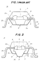
- FIG.1 shows an example of a conventional semiconductor device having the radiator structure.
- a radiator block 3 having a flange 3a is provided at a central opening part of inner leads 2a of a lead frame 2.
- the radiator block 3 has an inverted trapezoidal cross section. Ends of the inner leads 2a and the flange 3a of the radiator block 3 are fixed by calking at a calked part 4.
- a semiconductor chip 5 is mounted on the radiator block 3 by soldering, for example, and this semiconductor chip 5 is bonded to the inner leads 2a by wires 6. In other words, a die-bonding is made using one surface of the radiator block 3 as a stage.
- the semiconductor chip 5, the inner leads 2a and the like are encapsulated by a resin which is molded to form a package 7, and outer leads 2b are thereafter bent in an approximate S-shape or a gull-wing shape to suit the semiconductor device 1A for surface mounting.
- the radiator block 3 is mounted on the inner leads 2a at the calked part 4.
- the thickness of the lead frame 2 must be 300 to 400 ⁇ m at the minimum in order to enable the calking.
- the radiator block 3 is fixed to the lead frame 2, it is necessary to make the calking which limits the thickness of the lead frame 2.
- the radiator block 3 must be made of a metal.
- the adhesion of the radiator block 3 to the circuit substrate via an adhesive agent becomes poor when the semiconductor device 1A is mounted on the circuit substrate, because the adhesive agent used would naturally have good adhesion to the metal forming the radiator block 3 and not to the resin forming the resin burr or flash.
- the relatively heavy radiator block 3 which is made of a metal must hang from the lead frame 2 when molding the resin to form the package 7.
- the lead frame 2 is thin as described above to enable the calking, and it is difficult to stably support the radiator block 3 in the correct position during the molding process, and unwanted bends may be formed in the lead frame 2.
- US-A-3902148 discloses a package of the flip-chip type in which a tapered heat sink extends above the top surface of the package. Separate inner leads are used to attach the leads on the TAB tape to the chip, and two encapsulations are employed.
- a method of producing a semiconductor device including the following steps: (a) fitting a bottom part of a radiator block within a tapered hole formed at the bottom of a recess of a jig; (b) positioning on the jig a lead frame which has a central opening, so that the opening is located above the top surface of the radiator block; (c) mounting a semiconductor chip on the top surface of the radiator block and bonding the semiconductor chip to the lead frame by a plurality of wires; (d) positioning at least the radiator block on a lower metal die; (e) positioning an upper metal die on top of the lower metal die so as to form a cavity between them; and (f) injecting a resin into the cavity so as to mold the resin into apackage which encapsulates at least a part of the radiator block, the semiconductor chip, the wires and the inner parts of the leads of the lead frame, so that the outer parts of the leads of the lead frame extend outwardly of the package, while the bottom
- a semiconductor device comprising a lead frame having an opening at a central part thereof and a plurality of leads each made up of an inner part and an outer part; a radiator block provided under the opening of the lead frame, the radiator block having a top surface part and a bottom part, a gap being formed between the top surface part of the radiator block and the lead frame; a semiconductor chip mounted on the top surface part of the radiator block; a plurality of wires bonding the semiconductor chip and the leads; and a package which encapsulates at least a part of the radiator block, the semiconductor chip, the wires and the inner parts of the leads so that the outer parts of the leads extend outwardly of the package, the package filling the gap between the top surface part of the radiator block and the lead frame, and the bottom part of the radiator block projecting from the package by a predetermined length for conducting heat generated from the semiconductor chip outside the package; characterized in that the radiator block has a tapered shape, the size of the block decreasing towards the bottom surface thereof,
- the device of the present invention it is possible to obtain a satisfactory thermal conductivity by selecting an arbitrary material for the radiator block without being restricted in the selection, and the thickness of the lead frame does not need to be limited for the calking because no calking is require to produce this semiconductor device. Moreover, the mounting of the semiconductor device on a circuit substrate or the like is facilitated because the projecting length of the radiator block can be controlled with a high accuracy.
- the thickness of the lead frame will not be limited for the purpose of carrying out the calking.
- the jig is used to accurately position the radiator block when molding the resin to form the package, it is possible to suppress the generation of resin burr or flash during the molding process, and furthermore, it is possible to accurately control the projecting length of the radiator block by the thickness of the jig.
- FIG.2 shows an embodiment of a semiconductor device according to the present invention.
- those parts which are the same as those corresponding parts in FIG.1 are designated by the same reference numerals, and a description thereof will be omitted.
- an opening 11 is formed at the central part of the lead frame 2 on the inner side of the inner leads 2a.
- the radiator block 3 has an inverted trapezoidal cross section and is positioned below the opening 11 independently of the lead frame 2.
- This radiator block 3 is made of a material having a satisfactory thermal conductivity compared to the resin which forms the package 7, including metals such as aluminum and non-metals such as ceramics.
- the semiconductor chip 5 is mounted on the radiator block 3 by solder, silver paste or the like.
- the semiconductor chip 5 and the inner leads 2a are bonded by the wires 6.
- the semiconductor chip 5, the inner leads 2a and the like are encapsulated by a resin which is molded to form the package 7.
- a tip end 3b of the radiator block 3 projects from the bottom surface of the package 7 by a predetermined length.
- a tapered part 12 is formed on the radiator block 3 toward the tip end 3b.
- the outer leads 2b are bent in the S-shape or gull-wing shape to suit surface mounting of the semiconductor device 1B on a circuit substrate (not shown) or the like.
- the outer leads 2b may have other shapes, and may not be bent, depending on the kind of mounting used.
- a vertical length L1 of the outer lead 2b from the bottom surface of the package 7 is selected to 0.05 to 0.2 mm, for example.
- a projecting length L2 of the radiator block 3 from the bottom surface of the package 7 is selected so that L2 ⁇ L1 to suit surface mounting of the semiconductor device 1B. The surface mounting of the semiconductor device 1B on the circuit substrate will be described later.
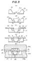
- FIG.3 a description will be given of an embodiment of a method of producing the semiconductor device according to the present invention, by referring to FIG.3.
- this embodiment of the method it is assumed for the sake of convenience that the embodiment of the semiconductor device 1B shown in FIG.2 is produced.
- This embodiment of the method uses a palette (jig) 21 shown in FIG.3 (A).
- This palette 21 has a recess 21a, a tapered hole 22 provided at the bottom of the palette 21, and positioning pins 23 provided on the palette 21 to position the lead frame 2.
- the palette 21 is made of a metal which has a coefficient of thermal expansion close to or approximately the same as that of the lead frame 2. For example, copper, copper-tin alloy or the like is used for the palette 21.
- the tip end 3b of the radiator block 3 is fit into the hole 22 of the palette 21 and positioned.
- the tapered part 12 of the radiator block 3 and the tapered shape of the wall defining the hole 22 correspond, and the positioning of the radiator block 3 can be made with a high accuracy.
- the inner leads 2a of the lead frame 2 are respectively provided with a positioning hole, and the positioning pins 23 fit into the positioning holes of the inner leads 2a when the lead frame 2 is placed on the palette 21 as shown in FIG.3 (C). Hence, the lead frame 2 is positioned on the palette 21 by the positioning pins 23.
- the semiconductor chip 5 is die-bonded on the radiator block 3 by solder, or silver paste for example, as shown in FIG.3 (D). Further, the semiconductor chip 5 and the inner leads 2a are bonded by the wires 6.
- FIG.3 (D) The structure shown in FIG.3 (D) is positioned within a cavity 24b1 of a lower metal die 24b shown in FIG.3 (E).
- a passage 25 is provided at the bottom of the cavity 24b1.
- One end of this passage 25 communicates to a part formed by the palette 21 and the radiator block 3, while the other end of this passage 25 is coupled to a vacuum source (not shown).
- a vacuum source not shown.
- an upper metal die 24a is positioned on top of the lower metal die 24b as shown in FIG.3 (E), and a resin is injected into a cavity 26 of the upper metal die 24a via a gate (not shown) so as to mold the resin and form the package 7.
- the vacuum suction is released, and the upper and lower metal dies 24a and 24b and the palette 21 are removed.
- the package 7 which has the tip end 3b of the radiator block 3 projecting by a predetermined length is obtained.
- the outer leads 2b are bent thereafter if necessary.
- the radiator block 3 can be made of a material other than metals.
- the radiator block 3 is positioned by the palette 21 under the vacuum suction, it is possible to accurately control the length of the tip end 3b of the radiator block 3 projecting from the package 7 by the thickness of the palette 21.
- the palette 21 and the radiator block 3 are positioned by the vacuum suction, it is possible to prevent the generation of resin burr or flash during the molding process.
- FIG.4 shows in more detail the palette 21 which is used in this embodiment of the method.
- FIG.4 (A) shows a side view of the palette 21, and
- FIG.4 (B) shows a plan view of palette 21.
- This palette 21 shown in FIG.4 integrally has three recesses 21a which are connected. However, for mass production purposes, it is of course possible to provide more than three recesses 21a.
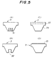
- FIG.5 shows modifications of the radiator block 3.
- the radiator block 3 shown in FIG.5 (A) has slits 31 formed on the tip end part thereof.
- the radiator block 3 has a fin shape, and the thermal conduction efficiency can be improved because the effect is basically the same as if the fins were directly mounted on the semiconductor chip 5.
- the radiator block 3 shown in FIG.5 (B) has a threaded part 32 formed on the tip end part thereof.
- an external radiator member can be screwed onto the radiator block 3 by a screw to improve the thermal conduction efficiency.
- the radiator block 3 shown in FIG.5 (C) has a mounting part 33 formed on top thereof.
- This mounting part 33 is made of copper, for example, and the semiconductor chip 5 is mounted on the mounting part 33.
- a part 34 of the radiator block 3 other than the mounting part 33 is made of a metal such as aluminum which is different from the metal forming the mounting part 33.
- the mounting part 33 and the part 34 are connected by thermocompression bonding. In this case, it is possible to mounting the semiconductor chip 5 on the mounting part 33 not only by silver paste but also by solder.
- the radiator block 3 is made mostly of aluminum, it is possible to reduce the weight of the semiconductor device 1B, and further, the surface of the aluminum can be subjected to an insulation process by an anodic oxidation.
- the mounting part 33 may be made of aluminum and the part 34 may be made of copper in FIG.5 (C).
- the radiator block 3 can be soldered directly when mounting the semiconductor device 1B on the circuit substrate.
- the radiator block 3 shown in FIG.5 (D) is made of a ceramic.
- the semiconductor chip 5 may be mounted on the radiator block 3 by silver paste.
- a metal layer 35 is provided on top of the radiator block 3, it is possible to mount the semiconductor chip 5 on the metal layer 35 by solder.
- the matching with the semiconductor chip 5 is particularly satisfactory because the coefficient of thermal expansion of the ceramic radiator block 3 becomes approximately the same as that of the semiconductor chip 5. Moreover, the ceramic radiator block 3 can be produced at a low cost, and the relatively rough surface of the ceramic provides good adherence to the circuit substrate when mounting the semiconductor device 1B onto the circuit substrate.
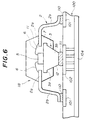
- FIG.6 a description will be given of the mounting of the semiconductor device 1B described above onto a circuit substrate, by referring to FIG.6.
- those parts which are the same as those corresponding parts in FIG.2 are designated by the same reference numerals, and a description thereof will be omitted.
- each outer lead 2b is connected to a contact 101 of a circuit substrate 100 by a solder 110.
- the tip end 3b of the radiator block 3 is adhered on a thermal conduction part 102 by an adhesive agent 111 having a satisfactory thermal conduction.
- the thermal conduction part 102 is made of a metal identical to that used for the radiator block 3. Therefore, the heat generated from the semiconductor chip 5 is transferred mainly through the radiator block 3 to the thermal conduction part 102 via the adhesive agent 111, and is finally released to a ground layer 104, for example. Because the projecting length of the tip end 3b of the radiator block 3 can be controlled with a high accuracy in the present invention, it is possible to improve the mounting of the semiconductor device 1B on the circuit substrate 100.
Landscapes
- Engineering & Computer Science (AREA)
- Microelectronics & Electronic Packaging (AREA)
- Computer Hardware Design (AREA)
- Physics & Mathematics (AREA)
- Condensed Matter Physics & Semiconductors (AREA)
- General Physics & Mathematics (AREA)
- Power Engineering (AREA)
- Manufacturing & Machinery (AREA)
- Chemical & Material Sciences (AREA)
- Materials Engineering (AREA)
- Cooling Or The Like Of Semiconductors Or Solid State Devices (AREA)
- Structures Or Materials For Encapsulating Or Coating Semiconductor Devices Or Solid State Devices (AREA)
- Encapsulation Of And Coatings For Semiconductor Or Solid State Devices (AREA)
Applications Claiming Priority (2)
| Application Number | Priority Date | Filing Date | Title |
|---|---|---|---|
| JP3275710A JP2602380B2 (ja) | 1991-10-23 | 1991-10-23 | 半導体装置及びその製造方法 |
| JP275710/91 | 1991-10-23 |
Publications (3)
| Publication Number | Publication Date |
|---|---|
| EP0539095A2 EP0539095A2 (en) | 1993-04-28 |
| EP0539095A3 EP0539095A3 (ja) | 1994-02-16 |
| EP0539095B1 true EP0539095B1 (en) | 1998-02-04 |
Family
ID=17559293
Family Applications (1)
| Application Number | Title | Priority Date | Filing Date |
|---|---|---|---|
| EP92309415A Expired - Lifetime EP0539095B1 (en) | 1991-10-23 | 1992-10-15 | Semiconductor device having radiator structure and method of producing the same |
Country Status (5)
| Country | Link |
|---|---|
| US (2) | US5444025A (ja) |
| EP (1) | EP0539095B1 (ja) |
| JP (1) | JP2602380B2 (ja) |
| KR (1) | KR960011643B1 (ja) |
| DE (1) | DE69224343T2 (ja) |
Families Citing this family (40)
| Publication number | Priority date | Publication date | Assignee | Title |
|---|---|---|---|---|
| JP3572628B2 (ja) * | 1992-06-03 | 2004-10-06 | セイコーエプソン株式会社 | 半導体装置及びその製造方法 |
| US5652461A (en) * | 1992-06-03 | 1997-07-29 | Seiko Epson Corporation | Semiconductor device with a convex heat sink |
| JP3362530B2 (ja) * | 1993-12-16 | 2003-01-07 | セイコーエプソン株式会社 | 樹脂封止型半導体装置およびその製造方法 |
| US5991156A (en) * | 1993-12-20 | 1999-11-23 | Stmicroelectronics, Inc. | Ball grid array integrated circuit package with high thermal conductivity |
| JP3509274B2 (ja) * | 1994-07-13 | 2004-03-22 | セイコーエプソン株式会社 | 樹脂封止型半導体装置およびその製造方法 |
| JP3367299B2 (ja) * | 1994-11-11 | 2003-01-14 | セイコーエプソン株式会社 | 樹脂封止型半導体装置およびその製造方法 |
| JP3542677B2 (ja) * | 1995-02-27 | 2004-07-14 | セイコーエプソン株式会社 | 樹脂封止型半導体装置およびその製造方法 |
| JP3309686B2 (ja) * | 1995-03-17 | 2002-07-29 | セイコーエプソン株式会社 | 樹脂封止型半導体装置及びその製造方法 |
| JPH08316372A (ja) * | 1995-05-16 | 1996-11-29 | Toshiba Corp | 樹脂封止型半導体装置 |
| JP2795626B2 (ja) * | 1995-08-21 | 1998-09-10 | 北川工業株式会社 | 放熱機能付き電子部品 |
| US5789270A (en) * | 1996-01-30 | 1998-08-04 | Industrial Technology Research Institute | Method for assembling a heat sink to a die paddle |
| DE69627643D1 (de) * | 1996-06-28 | 2003-05-28 | St Microelectronics Srl | Verfahren zur Herstellung einer Plastikpackung für eine elektronische Anordnung mit vollständig isolierter Wärmesenke |
| KR0185512B1 (ko) * | 1996-08-19 | 1999-03-20 | 김광호 | 칼럼리드구조를갖는패키지및그의제조방법 |
| DE69636853T2 (de) * | 1996-11-27 | 2007-11-08 | Stmicroelectronics S.R.L., Agrate Brianza | Herstellunsgverfahren einer Kunststoffpackung für elektronische Anordnungen mit einer Wärmesenke |
| KR19980039675A (ko) * | 1996-11-28 | 1998-08-17 | 황인길 | 반도체 패키지의 구조 |
| US6159764A (en) * | 1997-07-02 | 2000-12-12 | Micron Technology, Inc. | Varied-thickness heat sink for integrated circuit (IC) packages and method of fabricating IC packages |
| EP0895287A3 (en) | 1997-07-31 | 2006-04-05 | Matsushita Electric Industrial Co., Ltd. | Semiconductor device and lead frame for the same |
| US5917704A (en) * | 1997-10-06 | 1999-06-29 | Ford Motor Company | Laser-solderable electronic component |
| FR2778817B1 (fr) * | 1998-05-18 | 2000-06-30 | Remy Kirchdoerffer | Procede de fabrication d'un appareil ou d'un instrument par surmoulage et appareil ou instrument ainsi obtenu |
| JP2000150730A (ja) * | 1998-11-17 | 2000-05-30 | Fujitsu Ltd | 半導体装置及びその製造方法 |
| US6643919B1 (en) * | 2000-05-19 | 2003-11-11 | Siliconware Precision Industries Co., Ltd. | Method of fabricating a semiconductor device package having a core-hollowed portion without causing resin flash on lead frame |
| US6635209B2 (en) * | 2000-12-15 | 2003-10-21 | Siliconware Precision Industries Co., Ltd. | Method of encapsulating a substrate-based package assembly without causing mold flash |
| JP2002333552A (ja) | 2001-05-08 | 2002-11-22 | Fujitsu Ltd | 光装置 |
| US20030223181A1 (en) * | 2002-05-28 | 2003-12-04 | Micron Technology, Inc. | Electronic device package |
| US6987032B1 (en) | 2002-07-19 | 2006-01-17 | Asat Ltd. | Ball grid array package and process for manufacturing same |
| US6979594B1 (en) | 2002-07-19 | 2005-12-27 | Asat Ltd. | Process for manufacturing ball grid array package |
| US6800948B1 (en) | 2002-07-19 | 2004-10-05 | Asat Ltd. | Ball grid array package |
| US7372151B1 (en) | 2003-09-12 | 2008-05-13 | Asat Ltd. | Ball grid array package and process for manufacturing same |
| CN1323471C (zh) * | 2004-05-20 | 2007-06-27 | 中国科学院半导体研究所 | 具有倾斜波导结构的半导体光放大器封装用的热沉 |
| US8610262B1 (en) | 2005-02-18 | 2013-12-17 | Utac Hong Kong Limited | Ball grid array package with improved thermal characteristics |
| JP2007027535A (ja) * | 2005-07-20 | 2007-02-01 | Stanley Electric Co Ltd | 光半導体装置 |
| TW200812023A (en) * | 2006-08-22 | 2008-03-01 | Advanced Semiconductor Eng | Heat slug for package structure |
| GB2470802B (en) * | 2007-11-16 | 2011-10-05 | Uriel Meyer Wittenberg | A silver-based thermally conductive composition for thermally coupling LED chips to heat sinks |
| EP2293328B1 (en) * | 2008-06-12 | 2019-11-20 | Mitsubishi Electric Corporation | Method for manufacturing a power semiconductor circuit device |
| JP4973890B2 (ja) * | 2009-01-16 | 2012-07-11 | 住友電気工業株式会社 | リアクトル及びコイル成形体 |
| KR101092063B1 (ko) * | 2009-04-28 | 2011-12-12 | 엘지이노텍 주식회사 | 발광소자 패키지 및 그 제조방법 |
| KR101014063B1 (ko) | 2009-08-26 | 2011-02-10 | 엘지이노텍 주식회사 | 발광 소자 및 이를 이용한 라이트 유닛 |
| JP5714916B2 (ja) * | 2011-01-12 | 2015-05-07 | ルネサスエレクトロニクス株式会社 | 半導体装置およびその製造方法 |
| JP2013093504A (ja) * | 2011-10-27 | 2013-05-16 | Toshiba Corp | 半導体装置の製造方法および冶具 |
| DE102020106492A1 (de) * | 2019-04-12 | 2020-10-15 | Infineon Technologies Ag | Chip -package, verfahren zum bilden eines chip -packages, halbleitervorrichtung, halbleiteranordnung, dreiphasensystem, verfahren zum bilden einer halbleitervorrichtung und verfahren zum bilden einer halbleiteranordnung |
Family Cites Families (23)
| Publication number | Priority date | Publication date | Assignee | Title |
|---|---|---|---|---|
| US3414968A (en) * | 1965-02-23 | 1968-12-10 | Solitron Devices | Method of assembly of power transistors |
| CA892844A (en) * | 1970-08-14 | 1972-02-08 | H. Hantusch Gerald | Semiconductor heat sink |
| US3902148A (en) * | 1970-11-27 | 1975-08-26 | Signetics Corp | Semiconductor lead structure and assembly and method for fabricating same |
| JPS5315763A (en) * | 1976-07-28 | 1978-02-14 | Hitachi Ltd | Resin sealed type semiconductor device |
| FR2456390A1 (fr) * | 1979-05-11 | 1980-12-05 | Thomson Csf | Grille d'encapsulation, microboitier de circuit electronique utilisant cette grille et procede d'encapsulation de circuit electronique en microboitier |
| IT1218271B (it) * | 1981-04-13 | 1990-04-12 | Ates Componenti Elettron | Procedimento per la fabbricazione di contenitori in plastica con dissipatore termico per circuiti integrati e combinazione di stampo e dissipatori utilizzabile con tale procedimento |
| JPS58100447A (ja) * | 1981-12-11 | 1983-06-15 | Hitachi Ltd | 樹脂封止型半導体装置およびその製造方法 |
| FR2523397A1 (fr) * | 1982-03-08 | 1983-09-16 | Matra | Procede de montage de composants electroniques sur un support et produit realisable par le procede |
| JPH0666721B2 (ja) * | 1985-10-31 | 1994-08-24 | 株式会社東芝 | 衛星通信デマンドアサイン装置の回線使用状況伝達方法 |
| JPS62109326A (ja) * | 1985-11-07 | 1987-05-20 | Oki Electric Ind Co Ltd | 半導体装置の製造方法 |
| JPS62169450A (ja) * | 1986-01-22 | 1987-07-25 | Hitachi Ltd | 半導体装置 |
| US4890152A (en) * | 1986-02-14 | 1989-12-26 | Matsushita Electric Works, Ltd. | Plastic molded chip carrier package and method of fabricating the same |
| US5083373A (en) * | 1986-04-25 | 1992-01-28 | Hamburgen William R | Method for providing a thermal transfer device for the removal of heat from packaged elements |
| JPS63222450A (ja) * | 1987-03-11 | 1988-09-16 | Hitachi Chem Co Ltd | 半導体装置およびその製造法 |
| US5108955A (en) * | 1988-10-27 | 1992-04-28 | Citizen Watch Co., Ltd. | Method of making a resin encapsulated pin grid array with integral heatsink |
| JPH01268157A (ja) * | 1988-04-20 | 1989-10-25 | Ngk Spark Plug Co Ltd | ヒートシンク付セラミックパッケージ基板の製造方法 |
| JP2593702B2 (ja) * | 1988-11-09 | 1997-03-26 | 株式会社日立製作所 | 半導体装置の製造方法 |
| JPH02306639A (ja) * | 1989-05-22 | 1990-12-20 | Toshiba Corp | 半導体装置の樹脂封入方法 |
| JPH03180054A (ja) * | 1989-12-08 | 1991-08-06 | Matsushita Electron Corp | 樹脂封止型半導体装置 |
| JPH03214763A (ja) * | 1990-01-19 | 1991-09-19 | Nec Corp | 半導体集積回路装置のリードフレーム及びこれを用いた半導体集積回路装置 |
| US5147821A (en) * | 1990-09-28 | 1992-09-15 | Motorola, Inc. | Method for making a thermally enhanced semiconductor device by holding a leadframe against a heatsink through vacuum suction in a molding operation |
| US5345100A (en) * | 1991-03-29 | 1994-09-06 | Shindengen Electric Manufacturing Co., Ltd. | Semiconductor rectifier having high breakdown voltage and high speed operation |
| US5172213A (en) * | 1991-05-23 | 1992-12-15 | At&T Bell Laboratories | Molded circuit package having heat dissipating post |
-
1991
- 1991-10-23 JP JP3275710A patent/JP2602380B2/ja not_active Expired - Lifetime
-
1992
- 1992-10-15 DE DE69224343T patent/DE69224343T2/de not_active Expired - Fee Related
- 1992-10-15 EP EP92309415A patent/EP0539095B1/en not_active Expired - Lifetime
- 1992-10-23 KR KR1019920019495A patent/KR960011643B1/ko not_active IP Right Cessation
-
1994
- 1994-10-18 US US08/324,494 patent/US5444025A/en not_active Expired - Fee Related
-
1995
- 1995-04-13 US US08/421,448 patent/US5659200A/en not_active Expired - Fee Related
Also Published As
| Publication number | Publication date |
|---|---|
| EP0539095A3 (ja) | 1994-02-16 |
| EP0539095A2 (en) | 1993-04-28 |
| JP2602380B2 (ja) | 1997-04-23 |
| JPH05114669A (ja) | 1993-05-07 |
| US5659200A (en) | 1997-08-19 |
| KR930009039A (ko) | 1993-05-22 |
| DE69224343D1 (de) | 1998-03-12 |
| KR960011643B1 (ko) | 1996-08-24 |
| US5444025A (en) | 1995-08-22 |
| DE69224343T2 (de) | 1998-06-10 |
Similar Documents
| Publication | Publication Date | Title |
|---|---|---|
| EP0539095B1 (en) | Semiconductor device having radiator structure and method of producing the same | |
| US5198964A (en) | Packaged semiconductor device and electronic device module including same | |
| US6081029A (en) | Resin encapsulated semiconductor device having a reduced thickness and improved reliability | |
| EP0506509B1 (en) | Semiconductor device having radiation part and method of producing the same | |
| US5091341A (en) | Method of sealing semiconductor device with resin by pressing a lead frame to a heat sink using an upper mold pressure member | |
| KR100693241B1 (ko) | 반도체장치 | |
| US20050146057A1 (en) | Micro lead frame package having transparent encapsulant | |
| US5780933A (en) | Substrate for semiconductor device and semiconductor device using the same | |
| US6184575B1 (en) | Ultra-thin composite package for integrated circuits | |
| JPH06112354A (ja) | 薄型オーバーモールデッド半導体デバイスおよびその製造方法 | |
| US20020135076A1 (en) | Heat sink with collapse structure and semiconductor package with heat sink | |
| EP0484180A1 (en) | Packaged semiconductor device having an optimized heat dissipation | |
| JPH0473297B2 (ja) | ||
| JPS61168926A (ja) | 樹脂基板 | |
| EP0711104B1 (en) | Semiconductor device and method for making same | |
| JPH10112519A (ja) | 熱放散手段を有する集積回路装置及びその製造方法 | |
| JPH0870082A (ja) | 半導体集積回路装置およびその製造方法ならびにリードフレーム | |
| JPH08288428A (ja) | 樹脂封止型半導体装置 | |
| JP4688647B2 (ja) | 半導体装置とその製造方法 | |
| JPH0621124A (ja) | 半導体装置の製造方法 | |
| JPH02181956A (ja) | 半導体装置 | |
| JPH09129784A (ja) | 半導体装置およびその製造方法 | |
| JP2002009221A (ja) | 半導体装置及びその製造方法 | |
| KR100451488B1 (ko) | 반도체패키지및그제조방법 | |
| JPH0758246A (ja) | 半導体装置とその製造方法 |
Legal Events
| Date | Code | Title | Description |
|---|---|---|---|
| PUAI | Public reference made under article 153(3) epc to a published international application that has entered the european phase |
Free format text: ORIGINAL CODE: 0009012 |
|
| AK | Designated contracting states |
Kind code of ref document: A2 Designated state(s): DE FR GB |
|
| PUAL | Search report despatched |
Free format text: ORIGINAL CODE: 0009013 |
|
| AK | Designated contracting states |
Kind code of ref document: A3 Designated state(s): DE FR GB |
|
| 17P | Request for examination filed |
Effective date: 19940809 |
|
| 17Q | First examination report despatched |
Effective date: 19950825 |
|
| PGFP | Annual fee paid to national office [announced via postgrant information from national office to epo] |
Ref country code: LU Payment date: 19960901 Year of fee payment: 5 |
|
| GRAG | Despatch of communication of intention to grant |
Free format text: ORIGINAL CODE: EPIDOS AGRA |
|
| GRAH | Despatch of communication of intention to grant a patent |
Free format text: ORIGINAL CODE: EPIDOS IGRA |
|
| GRAH | Despatch of communication of intention to grant a patent |
Free format text: ORIGINAL CODE: EPIDOS IGRA |
|
| GRAA | (expected) grant |
Free format text: ORIGINAL CODE: 0009210 |
|
| AK | Designated contracting states |
Kind code of ref document: B1 Designated state(s): DE FR |
|
| REF | Corresponds to: |
Ref document number: 69224343 Country of ref document: DE Date of ref document: 19980312 |
|
| ET | Fr: translation filed | ||
| PLBE | No opposition filed within time limit |
Free format text: ORIGINAL CODE: 0009261 |
|
| STAA | Information on the status of an ep patent application or granted ep patent |
Free format text: STATUS: NO OPPOSITION FILED WITHIN TIME LIMIT |
|
| 26N | No opposition filed | ||
| PGFP | Annual fee paid to national office [announced via postgrant information from national office to epo] |
Ref country code: DE Payment date: 20061012 Year of fee payment: 15 |
|
| PG25 | Lapsed in a contracting state [announced via postgrant information from national office to epo] |
Ref country code: DE Free format text: LAPSE BECAUSE OF NON-PAYMENT OF DUE FEES Effective date: 20080501 |
|
| REG | Reference to a national code |
Ref country code: FR Ref legal event code: ST Effective date: 20080630 |
|
| PGFP | Annual fee paid to national office [announced via postgrant information from national office to epo] |
Ref country code: FR Payment date: 20061010 Year of fee payment: 15 |
|
| PG25 | Lapsed in a contracting state [announced via postgrant information from national office to epo] |
Ref country code: FR Free format text: LAPSE BECAUSE OF NON-PAYMENT OF DUE FEES Effective date: 20071031 |