EP0444580A2 - Dispositif d'affichage à cristal liquide - Google Patents
Dispositif d'affichage à cristal liquide Download PDFInfo
- Publication number
- EP0444580A2 EP0444580A2 EP91102767A EP91102767A EP0444580A2 EP 0444580 A2 EP0444580 A2 EP 0444580A2 EP 91102767 A EP91102767 A EP 91102767A EP 91102767 A EP91102767 A EP 91102767A EP 0444580 A2 EP0444580 A2 EP 0444580A2
- Authority
- EP
- European Patent Office
- Prior art keywords
- layer
- liquid crystal
- alloy
- electrodes
- disposed
- Prior art date
- Legal status (The legal status is an assumption and is not a legal conclusion. Google has not performed a legal analysis and makes no representation as to the accuracy of the status listed.)
- Granted
Links
Images

Classifications
-
- G—PHYSICS
- G02—OPTICS
- G02F—OPTICAL DEVICES OR ARRANGEMENTS FOR THE CONTROL OF LIGHT BY MODIFICATION OF THE OPTICAL PROPERTIES OF THE MEDIA OF THE ELEMENTS INVOLVED THEREIN; NON-LINEAR OPTICS; FREQUENCY-CHANGING OF LIGHT; OPTICAL LOGIC ELEMENTS; OPTICAL ANALOGUE/DIGITAL CONVERTERS
- G02F1/00—Devices or arrangements for the control of the intensity, colour, phase, polarisation or direction of light arriving from an independent light source, e.g. switching, gating or modulating; Non-linear optics
- G02F1/01—Devices or arrangements for the control of the intensity, colour, phase, polarisation or direction of light arriving from an independent light source, e.g. switching, gating or modulating; Non-linear optics for the control of the intensity, phase, polarisation or colour
- G02F1/13—Devices or arrangements for the control of the intensity, colour, phase, polarisation or direction of light arriving from an independent light source, e.g. switching, gating or modulating; Non-linear optics for the control of the intensity, phase, polarisation or colour based on liquid crystals, e.g. single liquid crystal display cells
- G02F1/133—Constructional arrangements; Operation of liquid crystal cells; Circuit arrangements
- G02F1/1333—Constructional arrangements; Manufacturing methods
- G02F1/1343—Electrodes
- G02F1/13439—Electrodes characterised by their electrical, optical, physical properties; materials therefor; method of making
Definitions
- the present invention relates to a liquid crystal device, particularly a device using a chiral smectic liquid crystal, and a display apparatus using such a device.
- a laminar structure of an ITO (indium-tin-oxide) electrode and a metal wire so as to provide a lower resistivity electrode structure for a liquid crystal display device.
- a metal constituting such a metal wire there has been used a metal, such as Cr (chromium), Mo (molybdenum), W (tungsten) or Ni (nickel), which can be selectively etched in combination with ITO and can also be subjected to an ordinary photolithographic process.
- Cr chromium
- Mo mobdenum
- W tungsten
- Ni nickel
- a laminate electrode structure of ITO and Al is formed by an ordinary lithographic process, there has been observed a difficulty that pinhole defects are liable to occur in the ITO film.
- a pattern of ITO electrode 2 is formed on a glass substrate 1 ( Figure 7A). Further, the ITO electrodes 2 are coated with an Al film 4 in a thickness of, e.g., 3000 ⁇ and then with a positive-type photoresist layer 5 ( Figure 7B). Then, a prescribed Al pattern is formed by an ordinary photolithographic process wherein the Al film 4 is etched by a developing liquid containing principally an organic alkali.
- FIGs 8A - 8E illustrate such an embodiment for production of a laminated electrode structure having a first layer of ITO 2, a second layer of Cr 9 and a third layer of Al 4.
- the production process is similar to the one explained with reference to Figures 7A - 7D except for the provision of the second Cr layer 9.
- the Al is partly preferentially dissolved during the developing step, but the occurrence of a pinhole in the ITO film is prevented due to the presence of the Cr layer 9 between the Al film 4 and the ITO film.
- An object of the present invention is to provide a liquid crystal device and a display apparatus having solved the above-mentioned problems.
- a more specific object of the present invention is to provide a liquid crystal device provided with electrodes with a reduced number of pinhole defects which are practically of no problem and a display apparatus using such a liquid crystal device.
- a liquid crystal device comprising a pair of oppositely disposed electrodes, and a liquid crystal disposed between the electrodes; wherein at least one of the pair of electrodes comprises a laminated structure including a first layer of indium tin oxide, a second layer of molybdenum or its alloy, and a third layer of aluminum or its alloy, disposed in the order named.
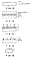
- Figures 1A - 1E illustrate a process for forming a laminated electrode structure on a substrate used in an embodiment of the liquid crystal device according to the invention.
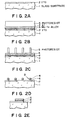
- Figures 2A - 2E illustrate a process for forming a laminated electrode structure on a substrate used in another embodiment of the liquid crystal device according to the invention.
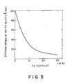
- Figure 3 is a graph showing a relationship between the etching speed of Mo - Ta alloy and the Ta content in the alloy.
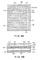
- Figure 4A is a schematic plan view of a ferroelectric liquid crystal device used in the invention
- Figure 4B is a sectional view taken along the line A-A therein.
- FIG. 5 is a block diagram of a liquid crystal display apparatus including a liquid crystal device and a graphic controller according to the invention
- Figure 6 is a time chart showing time correlation for image data communication between the liquid crystal device and the graphic controller.
- Figures 7A - 7D and Figures 8A - 8E respectively illustrate a conventional process for forming a laminated electrode structure on a substrate.
- the device of the present invention has been provided so as to remote the defects of the above-mentioned conventional laminated electrode structure. More specifically, according to the present invention, a layer of Mo or Mo alloy is interposed between an ITO electrode constituting a display electrode and a layer of Al or Al alloy, whereby a low-resistivity electrode including Al can be realized without complicating the production process or causing pinhole defects in the ITO electrode.
- a liquid crystal device may be formed by providing a pair of substrates having a display electrode having a laminated structure including a first layer of ITO, a second layer of Mo or Mo alloy disposed on the first layer, and a third layer of Al or Al alloy; subjecting the substrates to an aligning treatment; bonding the pair of substrates thus treated to each other with a gap therebetween; and filling the gap with a liquid crystal.
- such a display electrode may be formed on a substrate, e.g., through a process including the steps of: forming a film of ITO by sputtering on the substrate, forming the ITO film into a pattern of stripes by ordinary photolithographic technique, forming thereon laminated films of Mo or Mo alloy and Al or Al alloy sequentially by sputtering similarly as the ITO film, coating the laminated films with a positive-type photoresist layer which is then exposed and developed into a pattern, etching the layers of Al or Al alloy and Mo or Mo alloy with an etchant comprising a predominant amount of phosphoric acid and relatively small amounts of nitric acid, acetic acid and water, and then peeling the remaining photoresist film.
- the first layer of ITO may suitably be a conventional one having an Sn content of 1 - 10 wt. % and may suitably have a thickness of 500 ⁇ - 5000 ⁇ .
- the second layer comprises Mo or Mo alloy.
- the Mo alloy may suitably be Mo-Ta, Mo-Ti, Mo-Si, Mo-Cr, Mo-V, Mo-Nb, Mo-W, Mo-Ta-Ti, Mo-Ta-Si, Mo-Ta-V, etc.
- Such an Mo alloy is suitably be used because the etching speed thereof can be controlled by varying the content of an alloying element, such as Ta, Ti, ..., etc. ( Figure 3) preferably in a proportion of 1 - 30 wt. %, more preferably 5 - 20 wt. %. It is particularly preferred to use Mo-Ta or Mo-Ti alloy with a preferred Ta- or Ti-content of 30 wt. % or less, further preferably be 5 - 15 wt. %.
- the second layer of Mo or Mo alloy may be uniformly formed by vapor deposition on the ITO film and may desirably have a thickness of 50 - 2000 ⁇ , preferably 300 - 1000 ⁇ .
- a layer of Al or Al alloy is formed on the second layer of Mo or Mo alloy.
- the Al alloy may for example be Al-Si, Al-Cu-Si or Al-Ti alloys containing at least one alloying element selected from Si, Cu and Ti in a proportion of 1 - 5 wt. %.
- the Al or Al alloy can further contain Mo or Cr in a proportion of 1 - 5 wt. %.
- the Al or Al alloy layer may suitably have a thickness of 50 - 2000 ⁇ , preferably 300 - 1000 ⁇ .
- the liquid crystal used in the liquid crystal device may preferably be a ferroelectric liquid crystal which is not restricted to particular ones but can be selected from a wide scope.
- a laminated electrode structure was formed on a substrate through a process as illustrated in Figures 1A - 1E.
- a glass substrate 1 was coated with a 1000 ⁇ -thick ITO film by sputtering, which ITO film was then patterned into stripes 2 by ordinary photolithographic technique ( Figure 1A).
- the ITO stripes 2 were coated with laminated films including a 500 ⁇ -thick Mo film 3 and a 3000 ⁇ -thick Al film by sputtering similarly as the ITO film and then with a 1 micron-thick layer 5 of a positive-type photoresist (trade name: "OFPR-800", mfd. by Tokyo Ohka Kogyo K.K.) by using a roller coater ( Figure 1B). Then, the photoresist layer was exposed and then dipped in a developer liquid comprising principally an organic alkali (trade name: "NMD-3", mfd. by Tokyo Ohka Kogyo K.K.) to be patterned ( Figure 1C). In this step, Al 4 could be dissolved partly but the occurrence of pinholes in the ITO 2 was prevented due to the presence of the Mo film 2 between Al 4 and ITO 2 even if there were pinholes in the Al 4 film.
- a developer liquid comprising principally an organic alkali (trade name: "NM
- the laminated films of Al 4 and Mo were etched by an etching liquid comprising a mixture of phosphoric acid (98 wt. %), nitric acid (60 wt. %), acetic acid (100 wt. %) and water in volumetric ratios of 16:1:2:1, and then the photoresist 5 was peeled to leave a laminated electrode structure (Figure 1D).
- etching liquid comprising a mixture of phosphoric acid (98 wt. %), nitric acid (60 wt. %), acetic acid (100 wt. %) and water in volumetric ratios of 16:1:2:1, and then the photoresist 5 was peeled to leave a laminated electrode structure (Figure 1D).
- Mo showed a larger etching speed than Al with respect to the above etching liquid, so that slight overhangs of Al electrode were formed as shown in Figure 1E which is an enlarged view of a part A in Figure 1D.
- a pair of substrates each having thereon a laminated electrode structure thus formed were respectively subjected to an aligning treatment (including application of a polyimide film and rubbing of the polyimide film) and then bonded to each other with a gap therebetween, which was then filled with a ferroelectric chiral smectic liquid crystal (trade name: "CS-1014", mfd. by Chisso K.K.) to provide a liquid crystal display device.
- the liquid crystal display device resulted in alignment defects in the vicinity of the overhangs of Al electrodes, which were however so minute that they could be accepted without practical problem.
- a laminated electrode structure was formed on a substrate through a process as shown in Figures 2A - 2E, which was characterized by the use of an Mo-Ta alloy layer 6 as shown in Figures 2B - 2E instead of the Mo layer 3 in Example 1.
- Example 2 a pattern of ITO electrodes 2 was formed on a glass substrate 1 ( Figure 2A) and then coated with a 500 ⁇ -thick film 6 of Mo-Ta alloy (Mo 92.5 wt. %, Ta 7.5 wt. %) and a 3000 ⁇ -thick film 4 of Al, which were subjected to patterning in a similar process as in Example 1 ( Figures 2B - 2D).
- the etching speeds of Mo-Ta alloys were as shown in Figure 3 and could be controlled varying the Ta contents in the alloys.
- an Mo-Ta alloy containing 7.5 wt. % of Mo was used so as to provide an etching speed substantially identical to that of Al.
- a liquid crystal display device was prepared by using a pair of substrates thus processed otherwise in a similar manner as in Example 1.
- the display device provided a good display which was also free from alignment defects near the metal electrodes.
- Al electrodes were used as metal electrodes for providing a lower resistivity. It is however also possible to use an Al alloy such as Al-Si, Al-Si-Cu or Al-Ti in view of electro-migration and anti-corrosion characteristic. In this case, it is still possible to adjust the etching speed of Mo alloy to that of the Al alloy by changing the content of alloying element such as Ta or Ti, and also show the pinhole-preventing effect. These effects are applicable to any-types of liquid crystal display devices including STN, active matrix and ferroelectric chiral smectic liquid crystal devices.
- Figures 4A and 4B illustrate an embodiment of the liquid crystal device according to the present invention.
- Figure 4A is a plan view of the embodiment and
- Figure 4B is a sectional view taken along the line A-A in Figure 4A.
- a cell structure 100 shown in Figure 4 comprises a pair of substrates 101a and 101b made of glass plates or plastic plates which are held with a predetermined gap with spacers 104 and sealed with an adhesive 106 to form a cell structure.
- an electrode group e.g., an electrode group for applying scanning voltages of a matrix electrode structure
- a predetermined pattern e.g., of a stripe pattern.
- another electrode group e. g., an electrode group for applying signal voltages of the matrix electrode structure
- a plurality of laminated electrodes 102b intersecting with the electrodes 102a.
- an alignment control film 105 composed of an inorganic insulating material such as silicon monoxide, silicon dioxide, aluminum oxide, zirconia, magnesium fluoride, cerium oxide, cerium fluoride, silicon nitride, silicon carbide, and boron nitride, or an organic insulating material such as polyvinyl alcohol, polyimide, polyamide-imide, polyester-imide, polyparaxylylene, polyester, polycarbonate, polyvinyl acetal, polyvinyl chloride, polyamide, polystyrene, cellulose resin, melamine resin, urea resin and acrylic resin.
- an inorganic insulating material such as silicon monoxide, silicon dioxide, aluminum oxide, zirconia, magnesium fluoride, cerium oxide, cerium fluoride, silicon nitride, silicon carbide, and boron nitride
- an organic insulating material such as polyvinyl alcohol, polyimide, polyamide-imide, polyester-imide, polyparaxyly
- the alignment control film 105 may be formed by first forming a film of an inorganic insulating material or an organic insulating material as described above and then rubbing the surface thereof in one direction with velvet, cloth, paper, etc.
- the alignment control film 105 may be formed as a film of an inorganic insulating material such as SiO or SiO2 on the substrate 101b by the oblique or tilt vapor deposition.
- the alignment control film 105 also functions as an insulating film.
- the alignment control film may preferably have a thickness in the range of 100 ⁇ to 1 micron, especially 500 to 5000 ⁇ .
- the insulating film also has a function of preventing the occurrence of an electric current which is generally caused due to minor quantities of impurities contained in the liquid crystal layer 103, whereby deterioration of the liquid crystal compounds is prevented even on repeating operations.
- the liquid crystal device according to the present invention can have an alignment control film similar to the above-mentioned alignment control film 105 also on the other substrate 101a.
- the liquid crystal 103 in the cell structure 100 shown in Figure 3 may assume an SmC* (chiral smectic C) or SmH * (chiral smectic H) phase.
- SmC* or SmH* may be formed by phase transition from cholesteric phase which is a higher temperature phase than the smectic phase, particularly cholesteric phase having a grandjean texture, through SmA (smectic A) phase to SmC * or SmH * .
- the liquid crystal device further includes a sealant 106 composed of an epoxy adhesive, a pair of polarizers 107 and 108 disposed in cross nicols, and a heater 109 formed of a transparent resistor film (e.g., of SnO2).
- a sealant 106 composed of an epoxy adhesive
- a pair of polarizers 107 and 108 disposed in cross nicols
- a heater 109 formed of a transparent resistor film (e.g., of SnO2).
- Figure 5 is a block diagram showing an arrangement of a ferroelectric liquid crystal display apparatus 501 and a graphic controller 502 provided in an apparatus body of, e.g., a personal computer as a source of supplying display data.
- Figure 6 is a time chart for communication of image data.
- a display panel 503 (similar to a liquid crystal device 100 as described above) comprises a matrix electrode structure composed of 1120 scanning electrodes and 1280 data electrodes respectively disposed on a pair of glass plates and subjected to an aligning treatment, and a ferroelectric liquid crystal disposed between the glass substrates.
- the scanning electrodes (lines) and data electrodes (lines) are connected to a scanning line drive circuit 504 and a data line drive circuit 505, respectively.
- the graphic controller 502 supplies scanning line address data for designating a scanning line and image data (PD0 - PD3) on the scanning line designated by the address data to a display drive circuit 504/505 (composed of a scanning line drive circuit 504 and a data line drive circuit 505) of the liquid crystal display apparatus 501.
- the image data comprising the scanning line address data and the display data are transferred through the same transmission line, so that it is necessary to differentiate the above-mentioned two types of data.
- a signal AH/DL is used for the differentiation.
- the AH/DL signal at a high level means scanning line address data
- the AH/DL signal at a low level means display data.
- the scanning line address data are extracted from transferred image data PD0 - PD3 by a drive control circuit 511 and then supplied to the scanning line drive circuit 504 in synchronism with a time for driving a designated scanning line.
- the scanning line address data are inputted to a decoder 506 in the scanning line drive circuit 504, and a designated scanning line in the display panel 503 is driven by a scanning signal generating circuit 507 with the aid of the decoder 506.
- the display data are introduced to a shift register 508 in the data line drive circuit 505 and shifted by a unit of 4 pixel data based on a transfer clock signal.
- the shift register 508 When the shift of display data for one horizontal scanning line is completed by the shift register 508, the display data for 1280 pixels are transferred to a line memory disposed in parallel, memorized for a period of one horizontal scanning and are supplied to the respective data lines as display data signals through a data signal generating circuit 510.
- the drive of the display panel 503 in the liquid crystal display apparatus 501 is not synchronized with the generation of the scanning line address data and display data in the graphic controller 502, so that it is necessary to synchronize the apparatus 501 and 502 at the time of image data transfer.
- a signal SYNC is in charge of the synchronization and is generated in the drive control circuit 511 in the liquid crystal display apparatus 501 at each one horizontal scanning period.
- the graphic controller 502 always monitors the SYNC signal, and transfers image data when the SYNC signal is at a low level and does not effect transfer after completing transfer of image data for one horizontal scanning line when the SYNC signal is at high level.
- the graphic controller 502 immediately sets the AH/DL signal at high level and starts transfer of image data for one horizontal scanning line when it detects that the SYNC signal is at low level.
- the drive control circuit 511 in the liquid crystal display apparatus 501 set to the SYNC signal at high level during the image data transfer period.
- the drive controller circuit (FLCD controller) 511 returns the SYNC signal to the low level so that it can receive image data for a subsequent scanning line.
- a display electrode is constituted as a laminated structure including a second layer of Mo or Mo alloy between a first layer of ITO and a third layer of Al or Al alloy, whereby a liquid crystal display device having a low-resistivity electrode structure with the aid of an Al electrode without complicating the production process or causing pinhole defects in the ITO electrodes.
- a liquid crystal device is formed by disposing a liquid crystal between a pair of oppositely disposed electrodes, at least one of which has a laminated structure including a first layer of ITO (indium tin oxide), a second layer of Mo (molybdenum) or its alloy, and a third layer of Al (aluminum) or its alloy, disposed in the order named. Because of the Mo-based second layer, the ITO layer is protected during development of a photoresist layer formed on the Al-based third layer even if some pinholes are present in the Al-based third layer.
- the Mo-based second layer can be etched by an etchant for the Al-based third layer so that the entire process is not complicated because of the provision of the Mo-based second layer.
Landscapes
- Physics & Mathematics (AREA)
- Nonlinear Science (AREA)
- Mathematical Physics (AREA)
- Chemical & Material Sciences (AREA)
- Crystallography & Structural Chemistry (AREA)
- General Physics & Mathematics (AREA)
- Optics & Photonics (AREA)
- Liquid Crystal (AREA)
- Internal Circuitry In Semiconductor Integrated Circuit Devices (AREA)
- Electrodes Of Semiconductors (AREA)
- Weting (AREA)
- Laminated Bodies (AREA)
Applications Claiming Priority (2)
| Application Number | Priority Date | Filing Date | Title |
|---|---|---|---|
| JP2042611A JP2673460B2 (ja) | 1990-02-26 | 1990-02-26 | 液晶表示素子 |
| JP42611/90 | 1990-02-26 |
Publications (3)
| Publication Number | Publication Date |
|---|---|
| EP0444580A2 true EP0444580A2 (fr) | 1991-09-04 |
| EP0444580A3 EP0444580A3 (en) | 1992-03-11 |
| EP0444580B1 EP0444580B1 (fr) | 1996-06-05 |
Family
ID=12640827
Family Applications (1)
| Application Number | Title | Priority Date | Filing Date |
|---|---|---|---|
| EP91102767A Expired - Lifetime EP0444580B1 (fr) | 1990-02-26 | 1991-02-25 | Dispositif d'affichage à cristal liquide |
Country Status (6)
| Country | Link |
|---|---|
| US (2) | US5150233A (fr) |
| EP (1) | EP0444580B1 (fr) |
| JP (1) | JP2673460B2 (fr) |
| AT (1) | ATE139041T1 (fr) |
| DE (1) | DE69119928T2 (fr) |
| ES (1) | ES2089042T3 (fr) |
Cited By (5)
| Publication number | Priority date | Publication date | Assignee | Title |
|---|---|---|---|---|
| EP0536680A3 (en) * | 1991-10-07 | 1993-06-16 | Canon Kabushiki Kaisha | Liquid crystal device and liquid crystal injection method |
| US5361153A (en) * | 1991-06-12 | 1994-11-01 | Canon Kabushiki Kaisha | Electrode plate and process for production thereof |
| GB2283123A (en) * | 1993-10-23 | 1995-04-26 | Samsung Display Devices Co Ltd | Liquid crystal display |
| US6617541B1 (en) * | 1994-02-22 | 2003-09-09 | Koninklijke Philips Electronics N.V. | Laser etching method |
| US8405629B2 (en) | 2010-02-12 | 2013-03-26 | Plansee Se | Touch sensor configuration |
Families Citing this family (42)
| Publication number | Priority date | Publication date | Assignee | Title |
|---|---|---|---|---|
| JP2652072B2 (ja) * | 1990-02-26 | 1997-09-10 | キヤノン株式会社 | 遮光層の形成方法 |
| JP2673460B2 (ja) * | 1990-02-26 | 1997-11-05 | キヤノン株式会社 | 液晶表示素子 |
| US5367179A (en) * | 1990-04-25 | 1994-11-22 | Casio Computer Co., Ltd. | Thin-film transistor having electrodes made of aluminum, and an active matrix panel using same |
| US5243202A (en) * | 1990-04-25 | 1993-09-07 | Casio Computer Co., Ltd. | Thin-film transistor and a liquid crystal matrix display device using thin-film transistors of this type |
| JP2808480B2 (ja) * | 1990-07-18 | 1998-10-08 | キヤノン株式会社 | 液晶カラー表示素子用基板の製造方法 |
| JP2808483B2 (ja) * | 1990-08-30 | 1998-10-08 | キヤノン株式会社 | 液晶素子 |
| US5282068A (en) * | 1990-11-08 | 1994-01-25 | Canon Kabushiki Kaisha | Liquid crystal display with opaque insulating layer and metal layer at and wider than inter-electrode gap and method of manufacturing |
| JP2974520B2 (ja) * | 1991-10-25 | 1999-11-10 | キヤノン株式会社 | 電極基板及び液晶素子 |
| JPH05341315A (ja) * | 1992-06-08 | 1993-12-24 | Hitachi Ltd | 薄膜トランジスタ基板、液晶表示パネルおよび液晶表示装置 |
| US5821622A (en) * | 1993-03-12 | 1998-10-13 | Kabushiki Kaisha Toshiba | Liquid crystal display device |
| JP3106786B2 (ja) * | 1993-08-26 | 2000-11-06 | 松下電器産業株式会社 | 半導体装置およびその製造方法 |
| US5644415A (en) * | 1993-12-20 | 1997-07-01 | Casio Computer Co., Ltd. | Liquid crystal display device having wide field angle |
| DE69621396T2 (de) * | 1995-10-12 | 2002-11-14 | Canon K.K., Tokio/Tokyo | Flüssigkristallvorrichtung und Verfahren zu ihrer Herstellung |
| KR0161462B1 (ko) * | 1995-11-23 | 1999-01-15 | 김광호 | 액정 디스플레이에서의 게이트 패드 형성방법 |
| US6320639B1 (en) | 1996-03-11 | 2001-11-20 | Canon Kabushiki Kaisha | Liquid crystal device and process for production thereof |
| US6208400B1 (en) | 1996-03-15 | 2001-03-27 | Canon Kabushiki Kaisha | Electrode plate having metal electrodes of aluminum or nickel and copper or silver disposed thereon |
| GB2313226A (en) * | 1996-05-17 | 1997-11-19 | Sharp Kk | Addressable matrix arrays |
| US6106907A (en) * | 1996-06-25 | 2000-08-22 | Canon Kabushiki Kaisha | Electrode plate, liquid crystal device and production thereof |
| US6445004B1 (en) | 1998-02-26 | 2002-09-03 | Samsung Electronics Co., Ltd. | Composition for a wiring, a wiring using the composition, manufacturing method thereof, a display using the wiring and a manufacturing method thereof |
| US6337520B1 (en) * | 1997-02-26 | 2002-01-08 | Samsung Electronics Co., Ltd. | Composition for a wiring, a wiring using the composition, manufacturing method thereof, a display using the wiring and manufacturing method thereof |
| US6532053B2 (en) | 1996-12-18 | 2003-03-11 | Hitachi, Ltd. | Transverse electric field system liquid crystal display device suitable for improving aperture ratio |
| US6128053A (en) * | 1997-10-22 | 2000-10-03 | Mannesmann Vdo Ag | Liquid crystal display with heater |
| US6346175B1 (en) * | 1997-11-20 | 2002-02-12 | International Business Machines Corporation | Modification of in-plate refractory metal texture by use of refractory metal/nitride layer |
| US6184960B1 (en) | 1998-01-30 | 2001-02-06 | Sharp Kabushiki Kaisha | Method of making a reflective type LCD including providing a protective metal film over a connecting electrode during at least one portion of the manufacturing process |
| US6356327B1 (en) | 1999-03-29 | 2002-03-12 | National Semiconductor Corporation | Pixel array for silicon LC light valve featuring reflective metal surface underlying inter-pixel regions |
| US6233033B1 (en) * | 1999-03-29 | 2001-05-15 | National Semiconductor Corp. | Pixel array for LC silicon light valve featuring pixels with overlapping edges |
| US6577362B1 (en) | 1999-05-24 | 2003-06-10 | National Semiconductor Corporation | Pixel cell for silicon LC light valve having enhanced storage capacitance |
| KR100590916B1 (ko) * | 1999-06-23 | 2006-06-19 | 비오이 하이디스 테크놀로지 주식회사 | 박막 트랜지스터 어레이 기판의 제조방법 |
| US6373543B1 (en) | 1999-07-16 | 2002-04-16 | National Semiconductor Corporation | Process for forming silicon LC pixel cell having planar alignment layers of uniform thickness |
| KR100312328B1 (ko) * | 1999-08-06 | 2001-11-03 | 구본준, 론 위라하디락사 | 반사투과형 액정 표시장치 |
| KR100315648B1 (ko) * | 2000-01-21 | 2001-11-29 | 정지완 | 액정표시장치의 게이트 전극용 식각액 |
| JP3670577B2 (ja) * | 2000-01-26 | 2005-07-13 | シャープ株式会社 | 液晶表示装置およびその製造方法 |
| JP3617458B2 (ja) * | 2000-02-18 | 2005-02-02 | セイコーエプソン株式会社 | 表示装置用基板、液晶装置及び電子機器 |
| GB0029315D0 (en) * | 2000-12-01 | 2001-01-17 | Koninkl Philips Electronics Nv | Method of increasing the conductivity of a transparent conductive layer |
| KR100476050B1 (ko) * | 2001-09-01 | 2005-03-10 | 비오이 하이디스 테크놀로지 주식회사 | 반사형 액정표시장치 및 그의 제조방법 |
| CN100350570C (zh) * | 2001-10-22 | 2007-11-21 | 三菱瓦斯化学株式会社 | 铝/钼层叠膜的蚀刻方法 |
| US20030122987A1 (en) * | 2001-12-28 | 2003-07-03 | Myung-Joon Kim | Array substrate for a liquid crystal display device having multi-layered metal line and fabricating method thereof |
| JP4271915B2 (ja) * | 2002-04-11 | 2009-06-03 | オプトレックス株式会社 | 有機エレクトロルミネセンス表示素子、有機エレクトロルミネセンス表示装置 |
| JP4761425B2 (ja) * | 2004-05-12 | 2011-08-31 | 株式会社 日立ディスプレイズ | 表示装置および表示装置の製造方法 |
| US7642711B2 (en) * | 2004-07-06 | 2010-01-05 | Fujifilm Corporation | Functional layer having wiring connected to electrode and barrier metal between electrode and wiring |
| KR101061850B1 (ko) * | 2004-09-08 | 2011-09-02 | 삼성전자주식회사 | 박막 트랜지스터 표시판 및 그 제조방법 |
| JP6332019B2 (ja) * | 2014-12-25 | 2018-05-30 | セイコーエプソン株式会社 | 電気光学装置及びその製造方法、電子機器 |
Family Cites Families (14)
| Publication number | Priority date | Publication date | Assignee | Title |
|---|---|---|---|---|
| JPS57161882A (en) * | 1981-03-31 | 1982-10-05 | Hitachi Ltd | Display body panel |
| JPS62263676A (ja) * | 1986-05-09 | 1987-11-16 | Seiko Instr & Electronics Ltd | 薄膜トランジスタの製造方法 |
| US4853296A (en) * | 1986-10-22 | 1989-08-01 | Toppan Printing Co., Ltd. | Electrode plate for color display device |
| US4859036A (en) * | 1987-05-15 | 1989-08-22 | Canon Kabushiki Kaisha | Device plate having conductive films selected to prevent pin-holes |
| JPS63289533A (ja) * | 1987-05-22 | 1988-11-28 | Oki Electric Ind Co Ltd | 液晶ディスプレイ装置 |
| US5000545A (en) * | 1987-05-28 | 1991-03-19 | Canon Kabushiki Kaisha | Liquid crystal device with metal electrode partially overlying transparent electrode |
| JP2698357B2 (ja) * | 1987-08-17 | 1998-01-19 | キヤノン株式会社 | 電極間の短絡部分離法及び液晶パネルの製造法 |
| JPH01179915A (ja) * | 1988-01-11 | 1989-07-18 | Canon Inc | 液晶素子 |
| US5187601A (en) * | 1988-03-07 | 1993-02-16 | Semiconductor Energy Laboratory Co., Ltd. | Method for making a high contrast liquid crystal display including laser scribing opaque and transparent conductive strips simultaneously |
| JPH02132833A (ja) * | 1988-11-11 | 1990-05-22 | Matsushita Electric Ind Co Ltd | 薄膜配線 |
| JPH02228629A (ja) * | 1989-02-28 | 1990-09-11 | Sharp Corp | 液晶表示装置 |
| JP2673460B2 (ja) * | 1990-02-26 | 1997-11-05 | キヤノン株式会社 | 液晶表示素子 |
| JPH04116620A (ja) * | 1990-09-07 | 1992-04-17 | Sharp Corp | 液晶表示装置 |
| JP2952075B2 (ja) * | 1991-06-12 | 1999-09-20 | キヤノン株式会社 | 液晶素子の製造法 |
-
1990
- 1990-02-26 JP JP2042611A patent/JP2673460B2/ja not_active Expired - Fee Related
-
1991
- 1991-02-21 US US07/658,501 patent/US5150233A/en not_active Expired - Lifetime
- 1991-02-25 ES ES91102767T patent/ES2089042T3/es not_active Expired - Lifetime
- 1991-02-25 DE DE69119928T patent/DE69119928T2/de not_active Expired - Fee Related
- 1991-02-25 AT AT91102767T patent/ATE139041T1/de not_active IP Right Cessation
- 1991-02-25 EP EP91102767A patent/EP0444580B1/fr not_active Expired - Lifetime
-
1995
- 1995-02-09 US US08/386,177 patent/US5543946A/en not_active Expired - Lifetime
Cited By (8)
| Publication number | Priority date | Publication date | Assignee | Title |
|---|---|---|---|---|
| US5361153A (en) * | 1991-06-12 | 1994-11-01 | Canon Kabushiki Kaisha | Electrode plate and process for production thereof |
| EP0536680A3 (en) * | 1991-10-07 | 1993-06-16 | Canon Kabushiki Kaisha | Liquid crystal device and liquid crystal injection method |
| US5285300A (en) * | 1991-10-07 | 1994-02-08 | Canon Kabushiki Kaisha | Liquid crystal device |
| US5406398A (en) * | 1991-10-07 | 1995-04-11 | Canon Kabushiki Kaisha | Liquid crystal injection method using dummy electrodes |
| GB2283123A (en) * | 1993-10-23 | 1995-04-26 | Samsung Display Devices Co Ltd | Liquid crystal display |
| GB2283123B (en) * | 1993-10-23 | 1997-10-22 | Samsung Display Devices Co Ltd | A method of forming an electrode for a liquid crystal display |
| US6617541B1 (en) * | 1994-02-22 | 2003-09-09 | Koninklijke Philips Electronics N.V. | Laser etching method |
| US8405629B2 (en) | 2010-02-12 | 2013-03-26 | Plansee Se | Touch sensor configuration |
Also Published As
| Publication number | Publication date |
|---|---|
| DE69119928D1 (de) | 1996-07-11 |
| JP2673460B2 (ja) | 1997-11-05 |
| JPH03246524A (ja) | 1991-11-01 |
| US5150233A (en) | 1992-09-22 |
| ATE139041T1 (de) | 1996-06-15 |
| DE69119928T2 (de) | 1996-11-28 |
| ES2089042T3 (es) | 1996-10-01 |
| EP0444580B1 (fr) | 1996-06-05 |
| EP0444580A3 (en) | 1992-03-11 |
| US5543946A (en) | 1996-08-06 |
Similar Documents
| Publication | Publication Date | Title |
|---|---|---|
| US5150233A (en) | Liquid crystal device and display apparatus with a three-layered electrode of ito, molybdenum, and aluminum | |
| US5995172A (en) | Tablet integrated liquid crystal display apparatus with less parallax | |
| US5000545A (en) | Liquid crystal device with metal electrode partially overlying transparent electrode | |
| US5321537A (en) | Method for producing chiral smectic liquid crystal device including masking areas between electrodes, rubbing, removing mask, and rubbing again | |
| EP0224243B1 (fr) | Dispositif de modulation optique et procédé de commande de celui-ci | |
| EP0518296B1 (fr) | Plaque d'électrode et son procédé de production | |
| TWI224710B (en) | Liquid crystal display device and its driving method | |
| WO2000020918A1 (fr) | Dispositif a cristaux liquides et appareil electronique | |
| JP2001255543A (ja) | 液晶表示装置 | |
| US5282068A (en) | Liquid crystal display with opaque insulating layer and metal layer at and wider than inter-electrode gap and method of manufacturing | |
| JPH0263019A (ja) | 光学変調素子 | |
| JP2000321556A (ja) | 液晶の配向状態転移方法及び液晶表示装置の駆動方法 | |
| JP2769879B2 (ja) | カイラルスメクチック液晶素子 | |
| US5702871A (en) | Liquid crystal display with low resistance electrode and method therefor | |
| JP3120343B2 (ja) | 液晶表示素子 | |
| US6606134B1 (en) | Reflective ferroelectric liquid crystal display and projection system | |
| JP2870500B2 (ja) | 反射型液晶表示装置 | |
| EP1042703A2 (fr) | Dispositif d'affichage | |
| JP2881030B2 (ja) | 液晶表示装置 | |
| JPS62100739A (ja) | 液晶表示装置 | |
| JP2566149B2 (ja) | 光学変調素子 | |
| JP2000047256A (ja) | 液晶表示素子 | |
| JP3544598B2 (ja) | 2端子スイッチング素子を有する配線基板 | |
| JP2001117100A (ja) | 液晶素子 | |
| JP2002268094A (ja) | 液晶表示装置 |
Legal Events
| Date | Code | Title | Description |
|---|---|---|---|
| PUAI | Public reference made under article 153(3) epc to a published international application that has entered the european phase |
Free format text: ORIGINAL CODE: 0009012 |
|
| 17P | Request for examination filed |
Effective date: 19910325 |
|
| AK | Designated contracting states |
Kind code of ref document: A2 Designated state(s): AT BE CH DE DK ES FR GB GR IT LI LU NL SE |
|
| PUAL | Search report despatched |
Free format text: ORIGINAL CODE: 0009013 |
|
| AK | Designated contracting states |
Kind code of ref document: A3 Designated state(s): AT BE CH DE DK ES FR GB GR IT LI LU NL SE |
|
| 17Q | First examination report despatched |
Effective date: 19930809 |
|
| GRAA | (expected) grant |
Free format text: ORIGINAL CODE: 0009210 |
|
| AK | Designated contracting states |
Kind code of ref document: B1 Designated state(s): AT BE CH DE DK ES FR GB GR IT LI LU NL SE |
|
| PG25 | Lapsed in a contracting state [announced via postgrant information from national office to epo] |
Ref country code: LI Effective date: 19960605 Ref country code: GR Free format text: LAPSE BECAUSE OF FAILURE TO SUBMIT A TRANSLATION OF THE DESCRIPTION OR TO PAY THE FEE WITHIN THE PRESCRIBED TIME-LIMIT Effective date: 19960605 Ref country code: DK Effective date: 19960605 Ref country code: CH Effective date: 19960605 Ref country code: BE Effective date: 19960605 Ref country code: AT Effective date: 19960605 |
|
| REF | Corresponds to: |
Ref document number: 139041 Country of ref document: AT Date of ref document: 19960615 Kind code of ref document: T |
|
| REF | Corresponds to: |
Ref document number: 69119928 Country of ref document: DE Date of ref document: 19960711 |
|
| GRAH | Despatch of communication of intention to grant a patent |
Free format text: ORIGINAL CODE: EPIDOS IGRA |
|
| ITF | It: translation for a ep patent filed | ||
| ET | Fr: translation filed | ||
| REG | Reference to a national code |
Ref country code: ES Ref legal event code: FG2A Ref document number: 2089042 Country of ref document: ES Kind code of ref document: T3 |
|
| REG | Reference to a national code |
Ref country code: ES Ref legal event code: FG2A Ref document number: 2089042 Country of ref document: ES Kind code of ref document: T3 |
|
| REG | Reference to a national code |
Ref country code: CH Ref legal event code: PL |
|
| PG25 | Lapsed in a contracting state [announced via postgrant information from national office to epo] |
Ref country code: LU Free format text: LAPSE BECAUSE OF NON-PAYMENT OF DUE FEES Effective date: 19970228 |
|
| PLBE | No opposition filed within time limit |
Free format text: ORIGINAL CODE: 0009261 |
|
| STAA | Information on the status of an ep patent application or granted ep patent |
Free format text: STATUS: NO OPPOSITION FILED WITHIN TIME LIMIT |
|
| 26N | No opposition filed | ||
| REG | Reference to a national code |
Ref country code: GB Ref legal event code: IF02 |
|
| PGFP | Annual fee paid to national office [announced via postgrant information from national office to epo] |
Ref country code: SE Payment date: 20030205 Year of fee payment: 13 |
|
| PGFP | Annual fee paid to national office [announced via postgrant information from national office to epo] |
Ref country code: FR Payment date: 20030210 Year of fee payment: 13 |
|
| PGFP | Annual fee paid to national office [announced via postgrant information from national office to epo] |
Ref country code: GB Payment date: 20030219 Year of fee payment: 13 |
|
| PGFP | Annual fee paid to national office [announced via postgrant information from national office to epo] |
Ref country code: NL Payment date: 20030226 Year of fee payment: 13 Ref country code: ES Payment date: 20030226 Year of fee payment: 13 |
|
| PGFP | Annual fee paid to national office [announced via postgrant information from national office to epo] |
Ref country code: DE Payment date: 20030306 Year of fee payment: 13 |
|
| PG25 | Lapsed in a contracting state [announced via postgrant information from national office to epo] |
Ref country code: GB Free format text: LAPSE BECAUSE OF NON-PAYMENT OF DUE FEES Effective date: 20040225 |
|
| PG25 | Lapsed in a contracting state [announced via postgrant information from national office to epo] |
Ref country code: SE Free format text: LAPSE BECAUSE OF NON-PAYMENT OF DUE FEES Effective date: 20040226 Ref country code: ES Free format text: LAPSE BECAUSE OF NON-PAYMENT OF DUE FEES Effective date: 20040226 |
|
| PG25 | Lapsed in a contracting state [announced via postgrant information from national office to epo] |
Ref country code: NL Free format text: LAPSE BECAUSE OF NON-PAYMENT OF DUE FEES Effective date: 20040901 Ref country code: DE Free format text: LAPSE BECAUSE OF NON-PAYMENT OF DUE FEES Effective date: 20040901 |
|
| EUG | Se: european patent has lapsed | ||
| GBPC | Gb: european patent ceased through non-payment of renewal fee |
Effective date: 20040225 |
|
| PG25 | Lapsed in a contracting state [announced via postgrant information from national office to epo] |
Ref country code: FR Free format text: LAPSE BECAUSE OF NON-PAYMENT OF DUE FEES Effective date: 20041029 |
|
| NLV4 | Nl: lapsed or anulled due to non-payment of the annual fee |
Effective date: 20040901 |
|
| REG | Reference to a national code |
Ref country code: FR Ref legal event code: ST |
|
| PG25 | Lapsed in a contracting state [announced via postgrant information from national office to epo] |
Ref country code: IT Free format text: LAPSE BECAUSE OF NON-PAYMENT OF DUE FEES Effective date: 20050225 |
|
| REG | Reference to a national code |
Ref country code: ES Ref legal event code: FD2A Effective date: 20040226 |