EP0360507A2 - Integrierte Schaltungshalbleiteranordnung mit verbesserter Einrichtung für Speiseleitungen - Google Patents
Integrierte Schaltungshalbleiteranordnung mit verbesserter Einrichtung für Speiseleitungen Download PDFInfo
- Publication number
- EP0360507A2 EP0360507A2 EP89309390A EP89309390A EP0360507A2 EP 0360507 A2 EP0360507 A2 EP 0360507A2 EP 89309390 A EP89309390 A EP 89309390A EP 89309390 A EP89309390 A EP 89309390A EP 0360507 A2 EP0360507 A2 EP 0360507A2
- Authority
- EP
- European Patent Office
- Prior art keywords
- power source
- source lines
- lines
- integrated circuit
- line
- Prior art date
- Legal status (The legal status is an assumption and is not a legal conclusion. Google has not performed a legal analysis and makes no representation as to the accuracy of the status listed.)
- Granted
Links
- 239000004065 semiconductor Substances 0.000 title claims abstract description 36
- 238000003491 array Methods 0.000 claims description 34
- 238000010586 diagram Methods 0.000 description 12
- 238000011960 computer-aided design Methods 0.000 description 7
- 238000000034 method Methods 0.000 description 4
- 230000010354 integration Effects 0.000 description 1
- 238000004519 manufacturing process Methods 0.000 description 1
- 238000012986 modification Methods 0.000 description 1
- 230000004048 modification Effects 0.000 description 1
- 239000000758 substrate Substances 0.000 description 1
Images


Classifications
-
- G—PHYSICS
- G11—INFORMATION STORAGE
- G11C—STATIC STORES
- G11C7/00—Arrangements for writing information into, or reading information out from, a digital store
-
- H—ELECTRICITY
- H01—ELECTRIC ELEMENTS
- H01L—SEMICONDUCTOR DEVICES NOT COVERED BY CLASS H10
- H01L27/00—Devices consisting of a plurality of semiconductor or other solid-state components formed in or on a common substrate
- H01L27/02—Devices consisting of a plurality of semiconductor or other solid-state components formed in or on a common substrate including semiconductor components specially adapted for rectifying, oscillating, amplifying or switching and having potential barriers; including integrated passive circuit elements having potential barriers
- H01L27/04—Devices consisting of a plurality of semiconductor or other solid-state components formed in or on a common substrate including semiconductor components specially adapted for rectifying, oscillating, amplifying or switching and having potential barriers; including integrated passive circuit elements having potential barriers the substrate being a semiconductor body
- H01L27/10—Devices consisting of a plurality of semiconductor or other solid-state components formed in or on a common substrate including semiconductor components specially adapted for rectifying, oscillating, amplifying or switching and having potential barriers; including integrated passive circuit elements having potential barriers the substrate being a semiconductor body including a plurality of individual components in a repetitive configuration
- H01L27/118—Masterslice integrated circuits
-
- H—ELECTRICITY
- H01—ELECTRIC ELEMENTS
- H01L—SEMICONDUCTOR DEVICES NOT COVERED BY CLASS H10
- H01L23/00—Details of semiconductor or other solid state devices
- H01L23/52—Arrangements for conducting electric current within the device in operation from one component to another, i.e. interconnections, e.g. wires, lead frames
- H01L23/522—Arrangements for conducting electric current within the device in operation from one component to another, i.e. interconnections, e.g. wires, lead frames including external interconnections consisting of a multilayer structure of conductive and insulating layers inseparably formed on the semiconductor body
- H01L23/528—Geometry or layout of the interconnection structure
- H01L23/5286—Arrangements of power or ground buses
-
- H—ELECTRICITY
- H01—ELECTRIC ELEMENTS
- H01L—SEMICONDUCTOR DEVICES NOT COVERED BY CLASS H10
- H01L2924/00—Indexing scheme for arrangements or methods for connecting or disconnecting semiconductor or solid-state bodies as covered by H01L24/00
- H01L2924/0001—Technical content checked by a classifier
- H01L2924/0002—Not covered by any one of groups H01L24/00, H01L24/00 and H01L2224/00
Definitions
- the present invention generally relates to a semiconductor integrated circuit device having an improved arrangement of power source lines. More particularly, the present invention is directed to an improvement in routing power source lines of a standard cell type LSI (large scale integrated circuit).
- LSI large scale integrated circuit
- Power consumption of LSI chips is trending to an increase with an increase in integration density and speeding up operation. Particularly, fineness of wiring patterns deteriorates resistance to electromigration and shortens the lifetime of LSI chips. From these viewpoints, effective and efficient power supply is required to fabricate reliable LSI chips. Further, automatic routing of power source lines by use of computer aided design (CAD) is required to reduce a time it takes to design LSI chips.
- CAD computer aided design
- FIG.1 is a plan view of a conventional standard cell type LSI chip.
- the chip includes main (primary) power source lines 1 - 6, secondary or auxiliary power source lines 7 - 16, functional blocks (modules) 17 - 20, and an input/output (I/O) circuit block 21.
- the functional blocks 17 - 20 provide respective logics. For example, an arithmetic logic unit (ALU) is formed by a functional block.
- the functional block 19 includes unit cell arrays 22 each providing an NAND circuit, for example.
- the main power source lines 1 - 6 extend to the vicinity of the functional blocks 17 - 20 from power source terminals (not shown) provided in the I/O circuit block 21.
- the auxiliary power source lines 7 - 14 extend to the functional blocks 17 - 20 from the main power source lines 1 - 6 close thereto.
- the auxiliary power source lines 15 and 16 couple the unit cell arrays 22 and the auxiliary power source lines 7 - 14.
- An auxiliary power source line extending above the unit cell arrays 22 supplies each of the unit cell arrays 22 with power.
- the conventional layout of power source lines shown in FIG. 1 presents the following disadvantages.
- the arrangement is not suitable for automatic routing power source lines.
- a mother power source line is arranged so as to surround the entire internal area in which a plurality of functional blocks are formed.
- Main power source lines extending in a first direction (lateral direction) are arranged so as to connect opposite portions of the mother power source line.
- Supporting power source lines extending on the opposite sides of each of the functional blocks are arranged in a second direction perpendicular to the first direction so as to connect the supporting power source lines or between the supporting power source lines and the mother power source line.
- Power source lines which provide unit cell arrays with power extend so as to connect the supporting power source lines arranged on both the sides of each functional block.
- the unit cell arrays are supplied with power only through the power source lines provided so as to connect the supporting power source lines extending only in the second direction. Therefore, the degree of freedom to route power source lines is poor. In other words, the aforementioned arrangements of power source lines are not suitable for automatic design of routing through CAD. Further, for the same reason, it is very difficult to make the distribution of current uniform over the power source lines.
- a general object of the present invention is to provide a semiconductor integrated circuit device having an improved arrangement of power source lines.
- a more specific object of the present invention is to provide a semiconductor integrated circuit device having an improved arrangement of power source lines which are suitable for automatic routing design by use of CAD.
- Another object of the present invention is to provide a semiconductor integrated circuit device having an improved arrangement of power source lines capable of uniformly supplying functional blocks with necessary power.
- a semiconductor integrated circuit device comprising a plurality of functional blocks each executing respective logic operations and arranged in an internal area on a semiconductor chip, a first power source line arranged so as to surround the internal area, the first power source line being a closed-loop line, second power source lines provided for the respective functional blocks so as to surround the respective functional blocks on the chip, each of the second power source lines being a closed-loop line, and third power source lines mutually connecting the second power source lines for the functional blocks and connecting the second power source lines and the first power source line.
- a semiconductor integrated circuit device comprising a plurality of functional blocks each executing respective logic operations and arranged in an internal area on a semiconductor chip, a first high-potential power source line arranged so as to surround the internal area, the high-potential first power source line being a closed-loop line, second high-potential power source lines provided for the respective functional blocks so as to surround the respective functional blocks on the chip, each of the second high-potential power source lines being a closed-loop line, third high-potential power source lines mutually connecting the second high-potential power source lines for the functional blocks and connecting the second high-potential power source lines and the first high-potential power source line.
- the device includes a first low-potential power source line arranged so as to surround the internal area, the first low-potential power source line being a closed-loop line, second low-potential power source lines provided for the respective functional blocks so as to surround the respective functional blocks on the chip, each of the second low-potential power source lines being a closed-loop line, and third low-potential power source lines mutually connecting the second low-potential power source lines for the functional blocks and connecting the low-potential second power source lines and the first low-potential power source line.
- an integrated circuit chip 100 includes four functional blocks (modules) 17 - 20 such as an ALU or a RAM.
- Main power source lines (hereinafter simply referred to as main lines) 23 - 26 formed by closed loop lines are arranged so as to surround the functional blocks 17 - 20, respectively.
- a plurality of sub power source lines (hereinafter simply referred to sub-lines) 27 extend in the X and Y directions, and are arranged so as to connect the main lines 23 - 26 in the vicinity of the functional blocks 17 - 20.
- the main line 23 for the functional block 17 is connected to the main line 25 for the functional block 19 through the sub-lines 27 extending in the Y direction, and is connected to the main line 24 for the functional block 18 through the sub-lines 27 extending in the X direction.
- the main line 24 related to the functional block 18 is connected to both the main lines 25 and 26 through the sub-lines 27 extending in the Y direction.
- the sub-lines 27 further connect the main lines 23 - 26 to a trunk line 29, which is laid along the ends of the chip 100, and positioned between the I/O circuit block 21 and the functional blocks 23 - 26.
- Power source pads 30 provided in the I/O circuit block 21 are electrically connected to the trunk power source line 29.
- a line A denotes an imaginary boundary of the I/O circuit block 21 and an internal area in which the functional blocks 17 - 20 are located.
- Each of the functional blocks 17 - 20 provided in the internal area surrounded by the trunk power source line 29 is formed as follows.
- a plurality of unit cell arrays 22 (only two arrays are illustrated for the sake of simplicity in FIG.2) are provided in the X direction.
- Each of the unit cells forms a logic unit such as a NAND circuit.
- First local (auxiliary) power source lines (hereinafter simply referred to as first local lines) 28 related to the functional block 19 extend in the Y direction and are connected between opposite portions 25a and 25b of the sub-line 25 which extend in the X direction.
- the first local lines 28, which are illustrated by broken lines, are arranged at predetermined constant intervals. Alternatively, different sets of the adjacent first local lines 28 may be arranged at different intervals.
- Second local power source lines (hereinafter simply referred to as second local lines) 32 extend in the X direction and are connected between opposite portions 25c and 25d of the sub-line 25 which extend in the Y direction.
- the second local lines 32 are interposed between the adjacent unit cell arrays 22 or between each of the unit cell arrays 22 and each of the portions 25a and 25b of the sub-line 25.
- the number of second local lines 32 is not limited to one as illustrated in FIG.2, and an arbitrary number of second local lines 32 may be arranged between the adjacent unit cell arrays 22 or on the side of each of the unit cell arrays 22 which face the portions 25a and 25b of the main lines 25 extending in the X direction.
- Third local power source lines (hereinafter simply referred to as third local lines) 33 extend in the X direction and are laid on an insulating layer (not shown) formed on the unit cell arrays 22.
- the third local lines 33 are connected between the opposite portions 25c and 25d of the sub-line 25 which extend in the Y direction.
- a "black" dot denotes a via (through or contact) hole.
- the first local lines 28 are in contact with the unit cells through via holes and in contact with first and second local lines 32 and 33 through via holes. Via holes may be formed at intersecting points where the lines extending in the different directions intersect or may be formed in the vicinity thereof.
- FIG.3 is a cross sectional view taken along line III-III shown in FIG.2.
- An insulating layer 35 is deposited on the unit cell arrays 22 formed in a semiconductor substrate 39.
- the second and third local lines 32 and 33 extend on the insulating layer 35 in the X direction.
- the third local lines 33 are in contact with the corresponding unit cell arrays 22 through via holes 36 formed in the insulating layer 35.
- Signal lines 38 are also formed on the insulating layer 35.
- the second and third local lines 32 and 33, and the signal lines 38 positioned at a lower layer level are covered by an insulating layer 36, on which the first local line 28 extending in the Y direction is formed.
- the first local line 28 positioned at an upper layer level is in contact with the second and third local lines 32 and 33 through via holes 37 formed in the insulating layer 36.
- the trunk power source line 29 (not shown in FIG.3) is located at the upper or lower layer level.
- W1: W2: W3 are set to 8: 4: 1 where W1 is the width of each main line, W2 is the width of each sub-line, and W3 is the width of each local line.
- main lines 23 - 26, the sub-lines 27, and the local lines 28, 32 and 33 are of the same potential equal to a power source voltage V DD .
- Power source lines of a different potential equal to a power source voltage V SS are arranged in the same manner as the power source lines of V DD as shown in FIG.4.
- the arrangement shown in FIG.4 can be achieved by use of a multilevel layer structure.
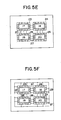
- FIG.5A the layout of the functional blocks 17 - 20 on the chip 100 are determined.
- the illustrated areas of the functional blocks 17 - 20 shown in FIGS.5A through 5F are of the same size for convenience' sake.
- FIG.5B the internal power source lines arranged in each of the functional blocks 17 - 20 are designed. That is, the layout of the first, second and third local lines 28, 32 and 33 are determined.
- the arrangement of signal lines 38 (FIG.3) in the functional blocks 17 - 20 is determined.
- the main lines 23 - 26 to be arranged around the functional blocks 17 - 20 are determined. Thereafter, as shown in FIG.5D, lines which connect the first to third local lines (power source terminals) provided in the functional blocks 17 - 20 and the relative main lines 23 - 26 are routed. After that, the layout of signal lines between the functional blocks 17 - 20 is determined. Then, as shown in FIG.5E, the sub-lines 27 are routed so as to connect the main lines 23 - 26. Finally, as shown in FIG.5F, the sub-lines 27 connecting the trunk power source line 29 and the main lines 17 - 20 are routed. It is noted that the above-mentioned procedure is somewhat different from an actual production procedure.
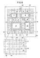
- a power source line 41 is arranged along the trunk power source line 29 so as to surround the internal area in which the functional blocks 17 - 20 are formed.
- the power source line 41 functions to make uniform the distribution of voltage (current) of the power source lines in the chip.
- FIG.7 is a diagram of a third embodiment of the present invention.
- those parts which are the same as those in FIGS.2 and 6 are given the same reference numerals.
- An essential feature of the third embodiment is that a power source line 42 is arranged so as to surround the functional blocks 17 and 18, and a power source line 43 is arranged so as to surround the functional blocks 19 and 20.
- the third embodiment can present the same advantage as the second embodiment.
- FIG.8 is a diagram illustrating a layout of main power source lines related to a functional block according to a fourth preferred embodiment of the present invention.
- a main power source line 45 is arranged so as to surround the functional block 19 in addition to the main line 25.
- the main line 45 is connected to the local lines extending from the functional block 19.
- the arrangement shown in FIG.8 is applicable to the other functional blocks 17, 18 and 20.
- the arrangement of the fourth embodiment makes uniform the distribution of voltage (current) of the power source lines in the chip.
- FIG.9 is a diagram illustrating a layout of main power source lines related to a functional block according to a fifth preferred embodiment of the present invention.
- a main power source line 46 has branch lines 46a and 46b extending in the Y direction.
- each of the line portions extending in the Y direction has a duplex arrangement. It is expected that a large amount of current passes through the duplex portions.
- FIG.10 is a diagram illustrating a variation of local power source lines extending in the X direction.
- Local power source lines 49 extending in the X direction are provided in a dead portion of a channel area.
- the local power source lines 49 contribute to making the distribution of voltage (current) uniform in the functional block 19.
- the arrangement of FIG.10 is applicable to the other functional blocks.
- FIG.11 illustrates an arrangement of power source lines associated with the functional block 19 in a case where the functional block 19 has a macrocell such as a RAM.
- the RAM provided in the functional block 19 together with the unit cell arrays 22 is surrounded by a part of the main line 25 and sub-lines 50 and 51.
- the sub-lines 50 and 51 extend in the Y and X directions, respectively.
- the sub-line 50 has the same width as the sub-line 27, and the sub-line 51 has the same width as each of the local lines 32, 33 and 28.
- Local lines 52 are provided so as to connect power source terminals of the RAM and the main line 25. Further, local lines 52 are provided so as to connect power source terminals of the RAM and the sub-lines 50 and 51. In this case, local lines 33b and 32b extending in the X direction are connected to the sub-line 50.
- the arrangement shown in FIG.11 can automatically be routed even when a macrocell such as a RAM is provided in a functional block.
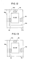
- FIG.12 illustrates a variation of the arrangement shown in FIG.11.
- the sub-line 50 shown in FIG.11 is formed by two sub-lines 50a and 50b extending in the Y direction.
- the sub-line 51 shown in FIG.11 is formed by two sub-lines 51a and 51b.
- An increased number of sub-lines 50 and 51 makes it possible to supply the RAM with sufficient power.
- the number of sub-lines 50 can arbitrarily be selected independent of the number of sub-lines 51 in view of necessary power.
- the sub-line 51 is a single line.
- FIGS.14 and 15 illustrate different variations of the arrangement shown in FIG.11.
- the RAM shown in each of FIGS.14 and 15 is positioned differently from the RAM shown in FIG.11.
- the RAM shown in FIG.14 is surrounded by a part of the main line 25 and sub-lines 50 and 51.
- Power source terminals of the RAM shown in FIG.14 are connected to the main line 25 and the sub-lines 50 and 51 through local lines 52.
- the RAM shown in FIG.15 is surrouned by sub-lines 53 and 54.
- Power source terminals of the RAM are connected to the sub-line 54 through local lines 52 extending in the X direction.
- Each of the lines 52 has the same width as the sub-line 27.
Landscapes
- Physics & Mathematics (AREA)
- Engineering & Computer Science (AREA)
- Power Engineering (AREA)
- Condensed Matter Physics & Semiconductors (AREA)
- General Physics & Mathematics (AREA)
- Computer Hardware Design (AREA)
- Microelectronics & Electronic Packaging (AREA)
- Geometry (AREA)
- Semiconductor Integrated Circuits (AREA)
- Design And Manufacture Of Integrated Circuits (AREA)
Applications Claiming Priority (2)
| Application Number | Priority Date | Filing Date | Title |
|---|---|---|---|
| JP234161/88 | 1988-09-19 | ||
| JP63234161A JP2668981B2 (ja) | 1988-09-19 | 1988-09-19 | 半導体集積回路 |
Publications (3)
| Publication Number | Publication Date |
|---|---|
| EP0360507A2 true EP0360507A2 (de) | 1990-03-28 |
| EP0360507A3 EP0360507A3 (de) | 1991-05-08 |
| EP0360507B1 EP0360507B1 (de) | 1994-08-10 |
Family
ID=16966615
Family Applications (1)
| Application Number | Title | Priority Date | Filing Date |
|---|---|---|---|
| EP89309390A Expired - Lifetime EP0360507B1 (de) | 1988-09-19 | 1989-09-15 | Integrierte Schaltungshalbleiteranordnung mit verbesserter Einrichtung für Speiseleitungen |
Country Status (5)
| Country | Link |
|---|---|
| US (1) | US5008728A (de) |
| EP (1) | EP0360507B1 (de) |
| JP (1) | JP2668981B2 (de) |
| KR (1) | KR920010982B1 (de) |
| DE (1) | DE68917398T2 (de) |
Cited By (1)
| Publication number | Priority date | Publication date | Assignee | Title |
|---|---|---|---|---|
| EP0735584A2 (de) * | 1995-03-30 | 1996-10-02 | AT&T Corp. | Integrierte Schaltung in Mehrlagen-Verbindungstechnik |
Families Citing this family (27)
| Publication number | Priority date | Publication date | Assignee | Title |
|---|---|---|---|---|
| US5349219A (en) * | 1989-06-15 | 1994-09-20 | Fujitsu Limited | Wafer-scale semiconductor integrated circuit device and method of forming interconnection lines arranged between chips of wafer-scale semiconductor integrated circuit device |
| JP2936542B2 (ja) * | 1990-01-30 | 1999-08-23 | 株式会社日立製作所 | 電源幹線のレイアウト方法 |
| US6759732B1 (en) | 1990-04-24 | 2004-07-06 | Seiko Epson Corporation | Semiconductor device with circuit cell array and arrangement on a semiconductor chip |
| JP3293135B2 (ja) * | 1990-04-24 | 2002-06-17 | セイコーエプソン株式会社 | 回路セル・アレイを備えた半導体装置 |
| US5300790A (en) * | 1990-06-15 | 1994-04-05 | Seiko Epson Corporation | Semiconductor device |
| US5321280A (en) * | 1990-09-13 | 1994-06-14 | Nec Corporation | Composite semiconductor integrated circuit device |
| US5283753A (en) * | 1991-07-25 | 1994-02-01 | Motorola, Inc. | Firm function block for a programmable block architected heterogeneous integrated circuit |
| US5155390A (en) * | 1991-07-25 | 1992-10-13 | Motorola, Inc. | Programmable block architected heterogeneous integrated circuit |
| JP2742735B2 (ja) * | 1991-07-30 | 1998-04-22 | 三菱電機株式会社 | 半導体集積回路装置およびそのレイアウト設計方法 |
| JP3052519B2 (ja) * | 1992-01-14 | 2000-06-12 | 日本電気株式会社 | 集積回路の電源配線設計方法 |
| US5313079A (en) * | 1992-06-22 | 1994-05-17 | Vlsi Technology, Inc. | Gate array bases with flexible routing |
| US5508938A (en) * | 1992-08-13 | 1996-04-16 | Fujitsu Limited | Special interconnect layer employing offset trace layout for advanced multi-chip module packages |
| JP2732762B2 (ja) * | 1992-09-21 | 1998-03-30 | 株式会社東芝 | 半導体記憶装置 |
| JPH0864768A (ja) * | 1994-08-18 | 1996-03-08 | Nec Corp | 半導体集積回路装置 |
| JP3432963B2 (ja) * | 1995-06-15 | 2003-08-04 | 沖電気工業株式会社 | 半導体集積回路 |
| JPH10189749A (ja) * | 1996-12-27 | 1998-07-21 | Toshiba Corp | 半導体集積回路装置、半導体集積回路装置の多電源供給方法、半導体集積回路装置の多電源供給プログラムを記録した機械読み取り可能な記録媒体 |
| US6683336B1 (en) | 1996-12-27 | 2004-01-27 | Kabushiki Kaisha Toshiba | Semiconductor integrated circuit, supply method for supplying multiple supply voltages in semiconductor integrated circuit, and record medium for storing program of supply method for supplying multiple supply voltages in semiconductor integrated circuit |
| KR100390464B1 (ko) * | 2000-09-27 | 2003-07-04 | 한국과학기술연구원 | 초미립 유전체 세라믹 조성물 |
| KR100406646B1 (ko) * | 2000-10-07 | 2003-11-21 | 한국과학기술연구원 | 고분자 매트릭스를 이용한 완화형 강유전체 세라믹스 후막 제조방법 |
| JP4737870B2 (ja) * | 2001-05-30 | 2011-08-03 | 東芝モバイルディスプレイ株式会社 | 液晶表示装置 |
| JP3786608B2 (ja) * | 2002-01-28 | 2006-06-14 | 株式会社ルネサステクノロジ | 半導体集積回路装置 |
| JP3964295B2 (ja) * | 2002-09-18 | 2007-08-22 | 松下電器産業株式会社 | 集積回路設計における電源経路構造 |
| JP3790202B2 (ja) | 2002-09-24 | 2006-06-28 | 松下電器産業株式会社 | 半導体集積回路の電源配線方法および半導体集積回路 |
| JP2004134599A (ja) * | 2002-10-11 | 2004-04-30 | Renesas Technology Corp | 半導体装置、およびそのレイアウト方法 |
| US6744081B2 (en) * | 2002-10-30 | 2004-06-01 | Lsi Logic Corporation | Interleaved termination ring |
| KR100615579B1 (ko) * | 2004-09-20 | 2006-08-25 | 삼성전자주식회사 | 반도체 메모리 장치 및 이 장치의 파워 라인 배치 방법 |
| JP5237739B2 (ja) | 2008-09-29 | 2013-07-17 | 株式会社日立製作所 | 情報処理装置 |
Citations (4)
| Publication number | Priority date | Publication date | Assignee | Title |
|---|---|---|---|---|
| JPS5694644A (en) * | 1979-12-27 | 1981-07-31 | Hitachi Ltd | Semiconductor ic device |
| EP0231821A2 (de) * | 1986-01-22 | 1987-08-12 | Nec Corporation | Stromversorgungsleitungen in einer integrierten Halbleiterschaltung |
| EP0295707A2 (de) * | 1987-06-19 | 1988-12-21 | Fujitsu Limited | Integrierte Halbleiterschaltungsanordnung mit Mehrschicht-Stromversorgungsleitungen |
| EP0307722A1 (de) * | 1987-08-31 | 1989-03-22 | Kabushiki Kaisha Toshiba | Halbleiteranordnung mit Mehrschichtleiter |
Family Cites Families (12)
| Publication number | Priority date | Publication date | Assignee | Title |
|---|---|---|---|---|
| JPS577140A (en) * | 1980-06-16 | 1982-01-14 | Pioneer Electronic Corp | Circuit device having plurality of circuit blocks |
| JPS57121250A (en) * | 1981-01-20 | 1982-07-28 | Toshiba Corp | Semiconductor integrated circuit |
| JPS58142559A (ja) * | 1982-02-19 | 1983-08-24 | Hitachi Ltd | 半導体集積回路装置 |
| US4568961A (en) * | 1983-03-11 | 1986-02-04 | Rca Corporation | Variable geometry automated universal array |
| JPS59207641A (ja) * | 1983-05-11 | 1984-11-24 | Hitachi Ltd | 集積回路 |
| JPS60101951A (ja) * | 1983-11-08 | 1985-06-06 | Sanyo Electric Co Ltd | ゲ−トアレイ |
| DE3585756D1 (de) * | 1984-07-02 | 1992-05-07 | Fujitsu Ltd | Halbleiterschaltungsanordnung in hauptscheibentechnik. |
| JPS61194739A (ja) * | 1985-02-22 | 1986-08-29 | Toshiba Corp | マスタ−スライス型半導体装置 |
| JPH07123139B2 (ja) * | 1986-03-28 | 1995-12-25 | 株式会社東芝 | 半導体論理集積回路装置のレイアウト方法 |
| JPS6395653A (ja) * | 1986-10-13 | 1988-04-26 | Nippon Telegr & Teleph Corp <Ntt> | 半導体集積回路電源供給方式 |
| JPS63152163A (ja) * | 1986-12-17 | 1988-06-24 | Hitachi Ltd | 半導体集積回路装置 |
| JPS644055A (en) * | 1987-06-25 | 1989-01-09 | Nec Corp | Construction of semiconductor integrated circuit |
-
1988
- 1988-09-19 JP JP63234161A patent/JP2668981B2/ja not_active Expired - Fee Related
-
1989
- 1989-09-14 US US07/409,553 patent/US5008728A/en not_active Expired - Lifetime
- 1989-09-15 EP EP89309390A patent/EP0360507B1/de not_active Expired - Lifetime
- 1989-09-15 DE DE68917398T patent/DE68917398T2/de not_active Expired - Fee Related
- 1989-09-19 KR KR1019890013475A patent/KR920010982B1/ko not_active IP Right Cessation
Patent Citations (4)
| Publication number | Priority date | Publication date | Assignee | Title |
|---|---|---|---|---|
| JPS5694644A (en) * | 1979-12-27 | 1981-07-31 | Hitachi Ltd | Semiconductor ic device |
| EP0231821A2 (de) * | 1986-01-22 | 1987-08-12 | Nec Corporation | Stromversorgungsleitungen in einer integrierten Halbleiterschaltung |
| EP0295707A2 (de) * | 1987-06-19 | 1988-12-21 | Fujitsu Limited | Integrierte Halbleiterschaltungsanordnung mit Mehrschicht-Stromversorgungsleitungen |
| EP0307722A1 (de) * | 1987-08-31 | 1989-03-22 | Kabushiki Kaisha Toshiba | Halbleiteranordnung mit Mehrschichtleiter |
Non-Patent Citations (2)
| Title |
|---|
| IEEE JOURNAL OF SOLID-STATE CIRCUITS, vol. SC-21, no. 1, February 1986, pages 150-156, IEEE, New York, US; W.S. SONG et al.: "Power distribution techniques for VLSI circuits" * |
| PATENT ABSTRACTS OF JAPAN, vol. 5, no. 167 (E-79)[839], 24th October 1981; & JP-A-56 094 644 (HITACHI SEISAKUSHO K.K.) 31-07-1981 * |
Cited By (2)
| Publication number | Priority date | Publication date | Assignee | Title |
|---|---|---|---|---|
| EP0735584A2 (de) * | 1995-03-30 | 1996-10-02 | AT&T Corp. | Integrierte Schaltung in Mehrlagen-Verbindungstechnik |
| EP0735584A3 (de) * | 1995-03-30 | 1997-12-29 | AT&T Corp. | Integrierte Schaltung in Mehrlagen-Verbindungstechnik |
Also Published As
| Publication number | Publication date |
|---|---|
| JP2668981B2 (ja) | 1997-10-27 |
| EP0360507A3 (de) | 1991-05-08 |
| DE68917398T2 (de) | 1994-12-01 |
| KR920010982B1 (ko) | 1992-12-26 |
| US5008728A (en) | 1991-04-16 |
| KR900005443A (ko) | 1990-04-14 |
| EP0360507B1 (de) | 1994-08-10 |
| DE68917398D1 (de) | 1994-09-15 |
| JPH0282552A (ja) | 1990-03-23 |
Similar Documents
| Publication | Publication Date | Title |
|---|---|---|
| US5008728A (en) | Semiconductor integrated circuit device having an improved arrangement of power source lines | |
| USRE39469E1 (en) | Semiconductor integrated circuit with mixed gate array and standard cell | |
| KR900003832B1 (ko) | 반도체 집적회로장치의 배선방법 | |
| US4811073A (en) | Gate array arrangement | |
| US6404226B1 (en) | Integrated circuit with standard cell logic and spare gates | |
| US5598347A (en) | Layout method for designing an integrated circuit device by using standard cells | |
| US4613941A (en) | Routing method in computer aided customization of a two level automated universal array | |
| US5977574A (en) | High density gate array cell architecture with sharing of well taps between cells | |
| US7523436B2 (en) | Semi-custom-made semiconductor integrated circuit device, method for customization and method for redesign | |
| US5095352A (en) | Semiconductor integrated circuit device of standard cell system | |
| US4568961A (en) | Variable geometry automated universal array | |
| US4499484A (en) | Integrated circuit manufactured by master slice method | |
| EP0072674B1 (de) | Halbleitervorrichtung mit einer Toranordnungsstruktur | |
| US5768146A (en) | Method of cell contouring to increase device density | |
| KR930003838B1 (ko) | 유니트 블록(unit block)구조를 갖는 바이폴라 집적회로 | |
| EP0848426A1 (de) | Integrierte Schaltungsanordnung und Verfahren zum Herstellen derselben | |
| US3983619A (en) | Large scale integrated circuit array of unit cells and method of manufacturing same | |
| EP0021661A1 (de) | Masterslice-Halbleitervorrichtung | |
| JP2000068383A (ja) | 半導体集積回路装置の設計方法および半導体集積回路装置 | |
| US5798541A (en) | Standard semiconductor cell with contoured cell boundary to increase device density | |
| USH512H (en) | Automated universal array | |
| CA1238986A (en) | Integrated circuit chip manufacture | |
| US5436801A (en) | Method and structure for routing power for optimum cell utilization with two and three level metal in a partially predesigned integrated circuit | |
| JPH01152642A (ja) | 半導体集積回路 | |
| GB2122417A (en) | Integrated circuits |
Legal Events
| Date | Code | Title | Description |
|---|---|---|---|
| PUAI | Public reference made under article 153(3) epc to a published international application that has entered the european phase |
Free format text: ORIGINAL CODE: 0009012 |
|
| AK | Designated contracting states |
Kind code of ref document: A2 Designated state(s): DE FR GB |
|
| PUAL | Search report despatched |
Free format text: ORIGINAL CODE: 0009013 |
|
| AK | Designated contracting states |
Kind code of ref document: A3 Designated state(s): DE FR GB |
|
| 17P | Request for examination filed |
Effective date: 19911031 |
|
| 17Q | First examination report despatched |
Effective date: 19931001 |
|
| GRAA | (expected) grant |
Free format text: ORIGINAL CODE: 0009210 |
|
| AK | Designated contracting states |
Kind code of ref document: B1 Designated state(s): DE FR GB |
|
| REF | Corresponds to: |
Ref document number: 68917398 Country of ref document: DE Date of ref document: 19940915 |
|
| ET | Fr: translation filed | ||
| PLBE | No opposition filed within time limit |
Free format text: ORIGINAL CODE: 0009261 |
|
| STAA | Information on the status of an ep patent application or granted ep patent |
Free format text: STATUS: NO OPPOSITION FILED WITHIN TIME LIMIT |
|
| 26N | No opposition filed | ||
| REG | Reference to a national code |
Ref country code: GB Ref legal event code: IF02 |
|
| PGFP | Annual fee paid to national office [announced via postgrant information from national office to epo] |
Ref country code: GB Payment date: 20060913 Year of fee payment: 18 |
|
| PGFP | Annual fee paid to national office [announced via postgrant information from national office to epo] |
Ref country code: DE Payment date: 20070913 Year of fee payment: 19 |
|
| PGFP | Annual fee paid to national office [announced via postgrant information from national office to epo] |
Ref country code: FR Payment date: 20070914 Year of fee payment: 19 |
|
| GBPC | Gb: european patent ceased through non-payment of renewal fee |
Effective date: 20070915 |
|
| PG25 | Lapsed in a contracting state [announced via postgrant information from national office to epo] |
Ref country code: GB Free format text: LAPSE BECAUSE OF NON-PAYMENT OF DUE FEES Effective date: 20070915 |
|
| REG | Reference to a national code |
Ref country code: FR Ref legal event code: ST Effective date: 20090529 |
|
| PG25 | Lapsed in a contracting state [announced via postgrant information from national office to epo] |
Ref country code: DE Free format text: LAPSE BECAUSE OF NON-PAYMENT OF DUE FEES Effective date: 20090401 |
|
| PG25 | Lapsed in a contracting state [announced via postgrant information from national office to epo] |
Ref country code: FR Free format text: LAPSE BECAUSE OF NON-PAYMENT OF DUE FEES Effective date: 20080930 |