EP0340731A2 - Ausgangsschaltung für eine integrierte Halbleiterschaltung mit reduziertem Speiseleitungsrauschen - Google Patents
Ausgangsschaltung für eine integrierte Halbleiterschaltung mit reduziertem Speiseleitungsrauschen Download PDFInfo
- Publication number
- EP0340731A2 EP0340731A2 EP89107943A EP89107943A EP0340731A2 EP 0340731 A2 EP0340731 A2 EP 0340731A2 EP 89107943 A EP89107943 A EP 89107943A EP 89107943 A EP89107943 A EP 89107943A EP 0340731 A2 EP0340731 A2 EP 0340731A2
- Authority
- EP
- European Patent Office
- Prior art keywords
- output
- buffer
- delay
- signal
- circuit
- Prior art date
- Legal status (The legal status is an assumption and is not a legal conclusion. Google has not performed a legal analysis and makes no representation as to the accuracy of the status listed.)
- Granted
Links
- 239000004065 semiconductor Substances 0.000 title claims abstract description 11
- 239000003990 capacitor Substances 0.000 claims abstract description 14
- 239000000872 buffer Substances 0.000 claims description 71
- 229910021420 polycrystalline silicon Inorganic materials 0.000 claims description 8
- 229920005591 polysilicon Polymers 0.000 claims description 7
- 238000010276 construction Methods 0.000 description 20
- 238000010586 diagram Methods 0.000 description 19
- 230000035515 penetration Effects 0.000 description 8
- 239000002184 metal Substances 0.000 description 5
- 238000009792 diffusion process Methods 0.000 description 4
- 230000001934 delay Effects 0.000 description 2
- 230000001939 inductive effect Effects 0.000 description 2
- 230000003071 parasitic effect Effects 0.000 description 2
- 230000015572 biosynthetic process Effects 0.000 description 1
- 230000003111 delayed effect Effects 0.000 description 1
- 238000012886 linear function Methods 0.000 description 1
- 229920000136 polysorbate Polymers 0.000 description 1
Images


Classifications
-
- H—ELECTRICITY
- H01—ELECTRIC ELEMENTS
- H01L—SEMICONDUCTOR DEVICES NOT COVERED BY CLASS H10
- H01L27/00—Devices consisting of a plurality of semiconductor or other solid-state components formed in or on a common substrate
- H01L27/02—Devices consisting of a plurality of semiconductor or other solid-state components formed in or on a common substrate including semiconductor components specially adapted for rectifying, oscillating, amplifying or switching and having at least one potential-jump barrier or surface barrier; including integrated passive circuit elements with at least one potential-jump barrier or surface barrier
- H01L27/04—Devices consisting of a plurality of semiconductor or other solid-state components formed in or on a common substrate including semiconductor components specially adapted for rectifying, oscillating, amplifying or switching and having at least one potential-jump barrier or surface barrier; including integrated passive circuit elements with at least one potential-jump barrier or surface barrier the substrate being a semiconductor body
- H01L27/06—Devices consisting of a plurality of semiconductor or other solid-state components formed in or on a common substrate including semiconductor components specially adapted for rectifying, oscillating, amplifying or switching and having at least one potential-jump barrier or surface barrier; including integrated passive circuit elements with at least one potential-jump barrier or surface barrier the substrate being a semiconductor body including a plurality of individual components in a non-repetitive configuration
-
- H—ELECTRICITY
- H01—ELECTRIC ELEMENTS
- H01L—SEMICONDUCTOR DEVICES NOT COVERED BY CLASS H10
- H01L29/00—Semiconductor devices adapted for rectifying, amplifying, oscillating or switching, or capacitors or resistors with at least one potential-jump barrier or surface barrier, e.g. PN junction depletion layer or carrier concentration layer; Details of semiconductor bodies or of electrodes thereof ; Multistep manufacturing processes therefor
- H01L29/40—Electrodes ; Multistep manufacturing processes therefor
- H01L29/43—Electrodes ; Multistep manufacturing processes therefor characterised by the materials of which they are formed
- H01L29/435—Resistive materials for field effect devices, e.g. resistive gate for MOSFET or MESFET
-
- H—ELECTRICITY
- H01—ELECTRIC ELEMENTS
- H01L—SEMICONDUCTOR DEVICES NOT COVERED BY CLASS H10
- H01L27/00—Devices consisting of a plurality of semiconductor or other solid-state components formed in or on a common substrate
- H01L27/02—Devices consisting of a plurality of semiconductor or other solid-state components formed in or on a common substrate including semiconductor components specially adapted for rectifying, oscillating, amplifying or switching and having at least one potential-jump barrier or surface barrier; including integrated passive circuit elements with at least one potential-jump barrier or surface barrier
-
- H—ELECTRICITY
- H03—ELECTRONIC CIRCUITRY
- H03K—PULSE TECHNIQUE
- H03K17/00—Electronic switching or gating, i.e. not by contact-making and –breaking
- H03K17/16—Modifications for eliminating interference voltages or currents
- H03K17/161—Modifications for eliminating interference voltages or currents in field-effect transistor switches
- H03K17/162—Modifications for eliminating interference voltages or currents in field-effect transistor switches without feedback from the output circuit to the control circuit
- H03K17/163—Soft switching
- H03K17/164—Soft switching using parallel switching arrangements
-
- H—ELECTRICITY
- H03—ELECTRONIC CIRCUITRY
- H03K—PULSE TECHNIQUE
- H03K19/00—Logic circuits, i.e. having at least two inputs acting on one output; Inverting circuits
-
- H—ELECTRICITY
- H03—ELECTRONIC CIRCUITRY
- H03K—PULSE TECHNIQUE
- H03K19/00—Logic circuits, i.e. having at least two inputs acting on one output; Inverting circuits
- H03K19/003—Modifications for increasing the reliability for protection
- H03K19/00346—Modifications for eliminating interference or parasitic voltages or currents
- H03K19/00361—Modifications for eliminating interference or parasitic voltages or currents in field effect transistor circuits
-
- H—ELECTRICITY
- H03—ELECTRONIC CIRCUITRY
- H03K—PULSE TECHNIQUE
- H03K2217/00—Indexing scheme related to electronic switching or gating, i.e. not by contact-making or -breaking covered by H03K17/00
- H03K2217/0036—Means reducing energy consumption
Definitions
- This invention relates to an output circuit of a semiconductor integrated circuit, and more particularly to the improvement for reduction in the power source noise occurring when a plurality of output circuits perform switching operations at the same time.
- resistive, capacitive and inductive loads are parasitically associated with the power source line of a semiconductor integrated circuit (IC).
- the inductive load in particular causes a large noise level when current flowing via the power source line changes abruptly.
- Such an abrupt change of current is caused by an output circuit for outputting a signal to the exterior of the IC. That is, it is necessary for the output circuit to extract a sufficiently large current from the power source line and charge or discharge a load capacitor outside the IC so as to drive the load capacitor at high speed.
- a plurality of output circuits of the same type as described above are used in the IC, and some of them perform switching operations at the same time.
- Fig. 6 is a circuit diagram showing the construction of the prior art output circuit provided in the MOS IC.
- Input signal In in the IC is supplied to buffer 24 having a CMOS inverter constituted by P-channel MOS transistor 22 and N-channel MOS transistor 23 via pre-buffer 21 constituted by an inverter.
- Output signal Out is output from the output terminal of buffer 24.
- buffer 24 is formed of one P-channel MOS transistor and one N-channel MOS transistor. Therefore, the current flowing out from power source voltage terminal Vcc and current flowing into ground voltage terminal Vss when output signal Out is changed are determined by the characteristics of the above transistors.
- the buffer of the output circuit is constituted by transistors having a large current driving ability, and the transistor is operated at a high switching speed.
- the noise occurring in the power source line increases even further, thereby causing the introduction of more noise into the signal of the output circuit.
- This invention has been made in consideration of the above situation, and an object of this invention is to provide an output circuit of a semiconductor integrated circuit capable of reducing the noise occurring in the power source lines at the time of a switching operation.
- the output circuit of the semiconductor integrated circuit of this invention includes a plurality of output transistors having different current driving abilities for a load; and a plurality of signal delay means for delaying signals for driving the respective output transistors by different delay times, wherein the plurality of output transistors are sequentially driven by outputs of the plurality of signal delay means whose signal delay times are set to be longer for the output transistors having larger load current driving abilities.
- the plurality of output transistors having different current driving abilities are sequentially driven with time delays.
- an output transistor having a larger current driving ability is driven with a longer delay time.
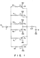
- Fig. 1 is a circuit diagram showing the construction of one embodiment of this invention applied to the output circuit of a MOS IC.
- 1 denotes a pre-buffer constituted by an inverter supplied with signal In in the IC.
- 20 to 2n denote output transistors of the P-channel section respectively constituting buffers for amplifying the output of pre-buffer 1 and outputting the amplified output as signal Out to the exterior of the IC.
- 30 to 3n denote output transistors of the N-channel section respectively constituting buffers.
- the sources of (n+1) output transistors 20 to 2n of the P-channel section are connected to power source potential terminal Vcc, and the drains thereof are commonly connected to a connection node for output signal Out.
- transistor 20 among output transistors 20 to 2n, transistor 20 has the largest current driving ability, and the current driving abilities of output transistors 20 to 2n become smaller respectively.
- the sources of (n+1) output transistors 30 to 3n of the N-channel section are connected to ground potential terminals Vss and the drains thereof are commonly connected to a node for output signal Out.
- transistor 30 Like the output transistors of the P-channel section, among (n+1) output transistors 30 to 3n of the N-channel section, transistor 30 has the largest current driving ability, and the current driving abilities of output transistors 30 to 3n become smaller respectively. Further, the entire current driving ability of output transistors 20 to 2n of the P-channel section is set equal to the current driving ability of one P-channel MOS transistor in the buffer of a conventional output circuit. Likewise, the entire current driving ability of output transistors 30 to 3n of the N-channel section is set equal to the current driving ability of one N-channel MOS transistor in the buffer of a conventional output circuit.
- resistors 40 to 4n which are formed of polysilicon, for example, are respectively connected between the output terminal of pre-buffer 1 and each of the gates of (n+1) output transistors 20 to 2n of the P-channel section.
- resistors 50 to 5n which are formed of polysilicon, for example, are respectively connected between the output terminal of pre-buffer 1 and each of the gates of (n+1) output transistors 30 to 3n of the N-channel section.
- resistor 4n has the smallest resistance, and the resistances of resistors 4n to 40 become larger respectively.
- resistor 5n has the smallest resistance, and the resistances of resistors 5n to 50 become larger respectively.
- Resistors 4 and 5 are respectively combined with gate input capacitors parasitically associated with the gates of respective P-channel MOS transistors 2 and N-channel MOS transistors 3 to constitute signal delay circuits.
- the signal delay circuits have CR time constants determined by the resistances of respective resistors 4 and 5 and capacitances of the respective gate input capacitors. That is, the signal delay times of the delay circuits are set in proportion to the resistances of the respective resistors 4 and 5. More specifically, the signal delay times associated with resistors 40 to 4n in the P-channel section become progressively shorter, and the signal delay times associated with resistors 50 to 5n in the N-channel section become progressively shorter.
- the output transistors in the P-channel and N-channel sections of the buffer are selectively driven with the signal delay times thereof being set to be longer for the output transistors having larger load current driving abilities.
- Capacitor 6 connected between a node for output signal Out and ground voltage terminal Vss shows an equivalent element of the external load driven by means of the output circuit.
- transistor 3n having the smallest current driving ability in the N-channel section is first turned on, thereby permitting output signal Out to be discharged towards ground voltage Vss via transistor 3n.
- the current driving ability of transistor 3n is small, the current flowing into the power source line of ground voltage Vss will not change abruptly.
- the outputs of the signal delay circuits are sequentially changed from Vss to Vcc in the order from the delay circuit having a shorter delay time to the delay circuit having a longer delay time. In this way, transistors 3 are sequentially turned on in the order from the transistor having a smaller current driving ability to the transistor having a larger current driving ability. Therefore, variation in current flowing into the power source line of ground voltage Vss with time can be suppressed to a minimum and kept constant.
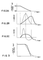
- Fig. 2B is a waveform diagram showing variations in the output currents in the conventional circuit and the circuit of the above embodiment, which are respectively indicated by broken and solid lines.
- Fig. 2C is a waveform diagram showing variations in the noise occurring in the power source lines when the above output currents flow in the conventional circuit and the circuit of the above embodiment, which are respectively indicated by broken and solid lines. As shown in Fig. 2C, the occurrence of power source noise in the circuit of the above embodiment is significantly reduced in comparison with the conventional case which is indicated by the broken line.
- Vout(t) Vcc - 1 C6 ⁇ I(t)dt ... (3) where C6 is the capacitance of load capacitor 6 and I(t) is a current flowing into the ground terminal.
- a plurality of output transistors are provided in each of the P-channel and N-channel sections of the buffer. Since the output transistors are sequentially turned on with respective time delays, noise occurring in the power source line can be significantly suppressed. Further, since the load current driving abilities of the output transistors of the P-channel and N-channel sections can be set at the same values as in the conventional case, high operation speeds and a high output circuit can be maintained. Since the power source noise can be suppressed, output noise in the output circuits which do not perform the switching operation can also be suppressed.
- Fig. 4 is a circuit diagram showing the construction of another embodiment of this invention which is applied to the output circuit of a MOS IC.
- resistors 4 and 5 which are combined with the respective gate input capacitors of output transistors 2 and 3 to constitute the signal delay circuits with respective CR time constants are connected between the output terminal of pre-buffer 1 and the gates of output transistors 2 and 3, respectively.
- (n+1) resistors 70 to 7n are series-connected between the output terminal of pre-buffer 1 and the gate of transistor 20 included in (n+1) output transistors 20 to 2n of the P-channel section and having the largest current driving ability.
- (n+1) resistors 80 to 8n are series-connected between the output terminal of pre-buffer 1 and the gate of transistor 30 included in (n+1) output transistors 30 to 3n of the P-channel section and having the largest current driving ability.
- delay signals derived from nodes of (n+1) resistors 70 to 7n of the P-channel section and respectively having gradually increasing delay times are sequentially supplied to the gates of output transistors 2n to 21 (in Fig. 4, transistor 21 is not shown).
- delay signals derived from nodes of (n+1) resistors 80 to 8n of the N-channel section and having gradually increasing delay times are sequentially supplied to the gates of output transistors 3n to 31 (in Fig. 4, transistor 31 is not shown).
- Fig. 5 is a circuit diagram showing the construction of still another embodiment of this invention which is applied to the output circuit of a MOS IC.
- the output of the pre-buffer is delayed by means of the signal delay circuits each constituted by the resistor and the gate input capacitor of the MOS transistor.
- the output terminals of pre-buffers 100 to 10n are respectively connected to CMOS inverters 90 to 9n which respectively include MOS transistors 20 to 2n of the P-channel section and MOS transistors 30 to 3n of the N-channel MOS transistors to constitute buffers.
- the current driving ability or circuit threshold voltage of each of pre-buffers 100 to 10n is determined according to the load current driving abilities of the MOS transistors constituting a corresponding one of CMOS inverters 90 to 9n.
- the signal delay time is determined according to the current driving ability thereof and the input capacitor of CMOS inverter 9 of the succeeding stage.
- the circuit threshold voltage of pre-buffer 10 the signal delay time is determined according to the threshold voltage thereof.
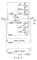
- Fig. 7 is a circuit diagram showing the construction of a transistor circuit according to still another embodiment of this invention and including a plurality of circuit blocks 1 to m in which part of the circuit shown in Fig. 4 is replaced by the circuit shown in Fig. 1.
- each of the connection nodes between series-connected resistors 10(0,0) to 10(i,0) is connected to a corresponding one of the gates of P-channel MOS transistors 12(0,0) to 12(i,0) in the same manner as in Fig. 4.
- each of the connection nodes between series-connected resistors 11(0,0) to 11(i,0) is connected to a corresponding one of the gates of N-channel MOS transistors 13(0,0) to 13(i,0).
- Subscripts i and j are integers which can be selectively set. That is, the gate of P-channel MOS transistor 12(i,0) is connected to freely selected connection node (i-1) of series-connected resistors 10(0,0) to 10(i,0) via resistor 10(i,0), and the gate of N-channel MOS transistor 13(i,0) is connected to freely selected connection node (i-1) of series-connected resistors 11(0,0) to 11(i,0) via resistor 11(i,0).
- P-channel MOS transistors 12(i,l) to 12(i,j), whose gates are respectively series-connected to resistors 10(i,l) to 10(i,j), are connected in parallel to the gate of P-channel MOS transistor 12(i,0), whose gate is series-connected to resistor 10(i,0), and an optional connection node.
- N-channel MOS transistors 13(i,l) to 13(i,j) whose gates are respectively series-connected to resistors 11(i,l) to 11(i,j), are connected in parallel to the gate of N-channel MOS transistor 13(i,0), whose gate is series-connected to resistor 11(i,0), and an optional node.
- Each of the drains of P-channel MOS transistors 12(0,0) to 12(i,j) and each of the drains of N-channel MOS transistors 13(0,0) to 13(i,j) are commonly connected to output terminal Out.
- the relation between the resistances of resistors 10(0,0) to 10(i,0) and resistors 11(0,0) to 11(i,0) is determined in the same manner as in the case of the relation between the resistances of resistors 70 to 7n and resistors 80 to 8n of Fig. 4. Further, the relation between the resistances of resistors 10(i,0) to 10(i,j) and resistors 11(i,0) to 11(i,j) is determined in the same manner as in the case of the relation between the resistances of resistors 40 to 4n and resistors 50 to 5n of Fig. 1.
- block 1 and blocks 2 to m having the same circuit construction as block 1 are connected in parallel (subscript numerals i and j may be differently set in each of blocks 1 to m).
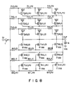
- Fig. 8 is a circuit diagram showing the construction of a transistor circuit according to another embodiment of this invention and corresponding to a circuit which is obtained by connecting a plurality of circuits shown in Fig. 4 in parallel.
- resistors 7(0,0) to 7(n,m) and resistors 8(0,0) to 8(n,m) are used to set the load driving abilities and load driving starting phases of the parallel-connected MOS transistors to different values, and it is not necessary to set the resistances of the resistors connected to the transistors on the same row in Fig. 8 to the same value.
- the output signal phase of pre-buffer 1 can be set so as to become larger in the order of Tp(0,0), Tp(0,1), ... Tp(0,m), Tp(1,0), Tp(1,1), ... Tp(1,m), Tp(n,0), Tp(n,1), ... and Tp(n,m) by adequately setting the resistances of the gate resistors of the P-channel MOS transistors.
- Fig. 9 is a circuit diagram showing the construction of still another embodiment of this invention including a plurality of circuit blocks for preventing penetration currents from flowing between power source terminals Vcc and Vss.
- the output signal of pre-buffer 1 In a case where the output signal of pre-buffer 1 is set to have different phases, the output signal of the pre-buffer for turning off the transistor which is driven by a signal with phase lag is set to have a corresponding phase lag.
- the P-channel MOS transistor and N-channel MOS transistor are simultaneously kept on for a longer period of time. In the period of time in which both the transistors are kept conductive, a penetration current will flow between power source terminals Vcc and Vss.
- P-channel MOS transistors T0P0 to T0Pn causing no phase delay (that is, having no delay resistor connected to the gate thereof) which results in occurrence of the simultaneous on-state, are inserted between each gate of P-Channel MOS buffer transistors TP(0,0) to TP(n,0) and power source terminal Vcc, and N-Channel MOS transistorsT0N0 to T0Nn having no delay resistor connected to the gate thereof and inserted between each gage of N-channel MOS buffer transistors TN(0,0) to TN(n,0) and power source terminal Vss.
- the gates of P-channel MOS transistors T0P0 to T0Pn and N-channel MOS transistors T0N0 to T0Nn are driven by the input signal of pre-buffer 1 without phase lag.
- the gates of transistors TP(0,0)to TP(N,0) and TN(0,0) to TN(n,0) are simultaneously driven by means of the transistors which are driven without phase lag, thereby preventing the penetration current flow.
- the circuit of Fig. 9 corresponds to a circuit obtained by adding the penetration current preventing circuit to the circuit of Fig. 4.
- Fig. 10 is a circuit diagram showing the construction of another embodiment of this invention including another circuit construction for preventing penetration currents from flowing between power source terminals Vcc and Vss.
- the circuit of Fig. 10 corresponds to a circuit obtained by applying the penetration current preventing transistors (T0P0 to T0Pn, T0N0 to T0Nn) to the parallel buffer transistors (20 to 2n, 30 to 3n).
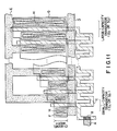
- Fig. 11 shows an IC pattern in which buffer MOS transistors (20 to 2n, 30 to 3n) are series-connected as in the case of Fig. 4.
- symbol A denotes output metal of pre-buffer 1
- symbol B denotes a metal-polysilicon contact hole
- symbol C denotes a polysilicon layer
- symbol D denotes source metal
- symbol E denotes drain metal
- symbol F denotes a source diffusion area
- symbol G denotes a drain diffusion area
- symbol H denotes a diffusion-metal contact hole.
- Polysilicon layer C is used for formation of a gate delay resistor.
- the channel width of a transistor section driven by a signal with relatively leading phase is narrow, and the channel width of a transistor section driven by a driving signal with larger phase lag is set wider (the transistor section having a wider channel width has a larger driving ability).
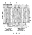
- Fig. 12 shows an IC pattern in which buffer MOS transistors are connected in parallel as in the case of Fig. 1.
- the channel width of a transistor in which a distance from contact hole B for pre-buffer output signal metal wiring A and gate polysilicon layer C to diffusion areas F and G is short (that is, the gate resistance is small) is set small
- the channel width of a transistor in which a distance from contact hole B to diffusion areas F and G is long (that is, the gate resistance is large) is set large.
- Fig. 13 shows an IC pattern in which buffer MOS transistors are connected in a series-parallel fashion as in the case of Fig. 7.
- a parasitic resistance component formed in the gate wiring portion when the gate of the transistor is formed by use of polysilicon layer C is used as a gate delay resistor.
- the driving abilities of the transistors are adjusted by the channel widths of the MOS transistors.
- the driving ability of the transistor can also be adjusted by changing the channel length, the gate oxide film thickness, or the threshold voltage of the transistor.
- a semiconductor integrated circuit can be provided which can suppress noise occurring in the power source line at the time of a switching operation.
Applications Claiming Priority (2)
| Application Number | Priority Date | Filing Date | Title |
|---|---|---|---|
| JP109312/88 | 1988-05-02 | ||
| JP63109312A JPH01279631A (ja) | 1988-05-02 | 1988-05-02 | 半導体集積回路の出力回路 |
Publications (3)
| Publication Number | Publication Date |
|---|---|
| EP0340731A2 true EP0340731A2 (de) | 1989-11-08 |
| EP0340731A3 EP0340731A3 (en) | 1990-05-23 |
| EP0340731B1 EP0340731B1 (de) | 1994-01-26 |
Family
ID=14507016
Family Applications (1)
| Application Number | Title | Priority Date | Filing Date |
|---|---|---|---|
| EP89107943A Expired - Lifetime EP0340731B1 (de) | 1988-05-02 | 1989-05-02 | Ausgangsschaltung für eine integrierte Halbleiterschaltung mit reduziertem Speiseleitungsrauschen |
Country Status (5)
| Country | Link |
|---|---|
| US (1) | US5128567A (de) |
| EP (1) | EP0340731B1 (de) |
| JP (1) | JPH01279631A (de) |
| KR (1) | KR930000970B1 (de) |
| DE (1) | DE68912640T2 (de) |
Cited By (8)
| Publication number | Priority date | Publication date | Assignee | Title |
|---|---|---|---|---|
| EP0298350A2 (de) * | 1987-07-10 | 1989-01-11 | Bayer Ag | Chirale 6-Hydroxymethylenverzweigte 3-Amino-4,5-dihydroxypiperidine, Zwischenprodukte zu ihrer Herstellung, Verfahren zu ihrer Herstellung und ihre Verwendung |
| EP0455572A2 (de) * | 1990-04-30 | 1991-11-06 | International Business Machines Corporation | CMOS-Treiber |
| WO1993014568A1 (de) * | 1992-01-14 | 1993-07-22 | Robert Bosch Gmbh | Treiberschaltung |
| EP1028528A1 (de) * | 1998-08-28 | 2000-08-16 | Matsushita Electric Industrial Co., Ltd. | Schaltregler und lsi-system |
| EP1056095A2 (de) * | 1997-01-06 | 2000-11-29 | Micron Technology, Inc. | Einstellbare Ausgangstreiberschaltung |
| WO2005057788A2 (de) * | 2003-12-11 | 2005-06-23 | Conti Temic Microelectronic Gmbh | Verfahren und schaltungsanordnung zur ansteuerung eines lastelements mittels eines elektronischen schaltelements im laststromkreis |
| EP1845619A1 (de) * | 2006-04-13 | 2007-10-17 | Stmicroelectronics Sa | Pufferkreis, der Mittel zur Steuerung der Steilheit des Ausgangssignals umfasst |
| US7417473B2 (en) * | 2005-05-30 | 2008-08-26 | Denso Corporation | Signal generator including current control element and signal forming element for achieving low noise level and low switching loss |
Families Citing this family (22)
| Publication number | Priority date | Publication date | Assignee | Title |
|---|---|---|---|---|
| US5231311A (en) * | 1989-02-28 | 1993-07-27 | Vlsi Technology, Inc. | Digital output buffer and method with slew rate control and reduced crowbar current |
| JP2616204B2 (ja) * | 1990-10-24 | 1997-06-04 | 日本電気株式会社 | 出力バッファ回路 |
| JPH04165669A (ja) * | 1990-10-29 | 1992-06-11 | Mitsubishi Denki Eng Kk | 集積化cmos出力回路 |
| JPH04248192A (ja) * | 1991-01-23 | 1992-09-03 | Nec Ic Microcomput Syst Ltd | 半導体記憶装置の出力回路 |
| JPH0555881A (ja) * | 1991-08-27 | 1993-03-05 | Toshiba Corp | 遅延回路 |
| US5287021A (en) * | 1992-05-06 | 1994-02-15 | Motorola, Inc. | Low noise BICMOS circuit |
| JPH06261386A (ja) * | 1993-03-05 | 1994-09-16 | Pioneer Electron Corp | ミューティング制御回路 |
| JP4467622B2 (ja) * | 1993-11-17 | 2010-05-26 | 株式会社ルネサステクノロジ | 出力回路 |
| US5694063A (en) * | 1994-08-11 | 1997-12-02 | Ltx Corporation | High speed IDDQ monitor circuit |
| US5552744A (en) * | 1994-08-11 | 1996-09-03 | Ltx Corporation | High speed IDDQ monitor circuit |
| JPH10290147A (ja) * | 1997-04-14 | 1998-10-27 | Mitsubishi Electric Corp | 遅延量可変回路 |
| US6177818B1 (en) | 1999-04-30 | 2001-01-23 | International Business Machines Corporation | Complementary depletion switch body stack off-chip driver |
| US6564173B1 (en) * | 2000-10-17 | 2003-05-13 | Daimlerchrysler Corporation | Remote multiplexed diagnostic circuitry and a method of detecting faults in sequentially driven loads |
| US6525569B1 (en) * | 2001-09-21 | 2003-02-25 | International Business Machines Corporation | Driver circuit having shapable transition waveforms |
| JP2004104940A (ja) * | 2002-09-11 | 2004-04-02 | Nidec Copal Corp | モータ駆動装置 |
| DE10355509A1 (de) * | 2003-11-27 | 2005-07-07 | Infineon Technologies Ag | Schaltung und Verfahren zum verzögerten Einschalten einer elektrischen Last |
| US7061301B2 (en) | 2003-12-19 | 2006-06-13 | Power Integrations, Inc. | Method and apparatus switching a semiconductor switch with a multi-state drive circuit |
| CN101765973A (zh) * | 2007-09-27 | 2010-06-30 | 松下电器产业株式会社 | 半导体集成电路装置、通信装置、信息再生装置、图像显示装置、电子装置、电子控制装置以及移动体 |
| KR100880924B1 (ko) * | 2007-12-20 | 2009-02-04 | 주식회사 하이닉스반도체 | 직류 대 직류 전압 변환 장치 |
| JP2012527178A (ja) | 2009-05-11 | 2012-11-01 | エスエス エスシー アイピー、エルエルシー | エンハンスメントモード型およびデプレションモード型のワイドバンドギャップ半導体jfetのためのゲートドライバ |
| US10483973B2 (en) | 2017-12-06 | 2019-11-19 | Taiwan Semiconductor Manufacturing Co., Ltd. | Temperature instability-aware circuit |
| US10505579B2 (en) * | 2018-02-02 | 2019-12-10 | Samsung Electro-Mechanics Co., Ltd. | Radio frequency switching device for fast switching operation |
Citations (6)
| Publication number | Priority date | Publication date | Assignee | Title |
|---|---|---|---|---|
| GB2177865A (en) * | 1985-07-12 | 1987-01-28 | Sony Corp | Output buffer circuit |
| EP0253914A1 (de) * | 1986-07-23 | 1988-01-27 | Deutsche ITT Industries GmbH | Isolierschicht-Feldeffekttransistor-Gegentakttreiberstufe mit Kompensierung von Betriebsparameterschwankungen und Fertigungsstreuungen |
| US4725747A (en) * | 1986-08-29 | 1988-02-16 | Texas Instruments Incorporated | Integrated circuit distributed geometry to reduce switching noise |
| EP0292641A2 (de) * | 1987-05-27 | 1988-11-30 | Kabushiki Kaisha Toshiba | Ausgangspuffer für MOS-integrierte Halbleiterschaltung |
| US4789793A (en) * | 1987-02-24 | 1988-12-06 | Texas Instruments Incorporated | Integrated FET circuit to reduce switching noise |
| US4820942A (en) * | 1988-01-27 | 1989-04-11 | Advanced Micro Devices, Inc. | High-speed, high-drive output buffer circuits with reduced ground bounce |
Family Cites Families (5)
| Publication number | Priority date | Publication date | Assignee | Title |
|---|---|---|---|---|
| JPS60141020A (ja) * | 1983-12-28 | 1985-07-26 | Nec Corp | Cmos論理回路 |
| US4700089A (en) * | 1984-08-23 | 1987-10-13 | Fujitsu Limited | Delay circuit for gate-array LSI |
| US4719369A (en) * | 1985-08-14 | 1988-01-12 | Hitachi, Ltd. | Output circuit having transistor monitor for matching output impedance to load impedance |
| JPS6248806A (ja) * | 1985-08-28 | 1987-03-03 | Nec Corp | 出力回路 |
| JPS63299513A (ja) * | 1987-05-29 | 1988-12-07 | Toshiba Corp | 出力回路 |
-
1988
- 1988-05-02 JP JP63109312A patent/JPH01279631A/ja active Pending
-
1989
- 1989-05-01 US US07/345,259 patent/US5128567A/en not_active Expired - Lifetime
- 1989-05-02 EP EP89107943A patent/EP0340731B1/de not_active Expired - Lifetime
- 1989-05-02 DE DE89107943T patent/DE68912640T2/de not_active Expired - Fee Related
- 1989-05-02 KR KR1019890005909A patent/KR930000970B1/ko not_active IP Right Cessation
Patent Citations (6)
| Publication number | Priority date | Publication date | Assignee | Title |
|---|---|---|---|---|
| GB2177865A (en) * | 1985-07-12 | 1987-01-28 | Sony Corp | Output buffer circuit |
| EP0253914A1 (de) * | 1986-07-23 | 1988-01-27 | Deutsche ITT Industries GmbH | Isolierschicht-Feldeffekttransistor-Gegentakttreiberstufe mit Kompensierung von Betriebsparameterschwankungen und Fertigungsstreuungen |
| US4725747A (en) * | 1986-08-29 | 1988-02-16 | Texas Instruments Incorporated | Integrated circuit distributed geometry to reduce switching noise |
| US4789793A (en) * | 1987-02-24 | 1988-12-06 | Texas Instruments Incorporated | Integrated FET circuit to reduce switching noise |
| EP0292641A2 (de) * | 1987-05-27 | 1988-11-30 | Kabushiki Kaisha Toshiba | Ausgangspuffer für MOS-integrierte Halbleiterschaltung |
| US4820942A (en) * | 1988-01-27 | 1989-04-11 | Advanced Micro Devices, Inc. | High-speed, high-drive output buffer circuits with reduced ground bounce |
Non-Patent Citations (1)
| Title |
|---|
| ELECTRO 1988 CONFERENCE RECORD, vol. 13, 10th-12th May 1988, paper 41/1, pages 1-4; S. ANDERSON et al.: "Investigation of the performance of advanced CMOS ouput buffers in a transmission line environment" * |
Cited By (16)
| Publication number | Priority date | Publication date | Assignee | Title |
|---|---|---|---|---|
| EP0298350A3 (de) * | 1987-07-10 | 1990-07-25 | Bayer Ag | Chirale 6-Hydroxymethylenverzweigte 3-Amino-4,5-dihydroxypiperidine, Zwischenprodukte zu ihrer Herstellung, Verfahren zu ihrer Herstellung und ihre Verwendung |
| EP0298350A2 (de) * | 1987-07-10 | 1989-01-11 | Bayer Ag | Chirale 6-Hydroxymethylenverzweigte 3-Amino-4,5-dihydroxypiperidine, Zwischenprodukte zu ihrer Herstellung, Verfahren zu ihrer Herstellung und ihre Verwendung |
| EP0455572A2 (de) * | 1990-04-30 | 1991-11-06 | International Business Machines Corporation | CMOS-Treiber |
| EP0455572A3 (en) * | 1990-04-30 | 1992-01-08 | International Business Machines Corporation | Complementary mos driver device |
| WO1993014568A1 (de) * | 1992-01-14 | 1993-07-22 | Robert Bosch Gmbh | Treiberschaltung |
| EP1056095A3 (de) * | 1997-01-06 | 2000-12-20 | Micron Technology, Inc. | Einstellbare Ausgangstreiberschaltung |
| EP1056095A2 (de) * | 1997-01-06 | 2000-11-29 | Micron Technology, Inc. | Einstellbare Ausgangstreiberschaltung |
| EP1028528A4 (de) * | 1998-08-28 | 2001-10-10 | Matsushita Electric Ind Co Ltd | Schaltregler und lsi-system |
| EP1028528A1 (de) * | 1998-08-28 | 2000-08-16 | Matsushita Electric Industrial Co., Ltd. | Schaltregler und lsi-system |
| US6429633B1 (en) | 1998-08-28 | 2002-08-06 | Matsushita Electric Industrial Co., Ltd. | Switching regulator and LSI system |
| WO2005057788A2 (de) * | 2003-12-11 | 2005-06-23 | Conti Temic Microelectronic Gmbh | Verfahren und schaltungsanordnung zur ansteuerung eines lastelements mittels eines elektronischen schaltelements im laststromkreis |
| WO2005057788A3 (de) * | 2003-12-11 | 2005-07-28 | Conti Temic Microelectronic | Verfahren und schaltungsanordnung zur ansteuerung eines lastelements mittels eines elektronischen schaltelements im laststromkreis |
| US8035363B2 (en) | 2003-12-11 | 2011-10-11 | Conti Temic Microelectronic, Gmbh | Procedure and a switching arrangement for triggering a load element using an electronic switching element in a load circuit |
| US7417473B2 (en) * | 2005-05-30 | 2008-08-26 | Denso Corporation | Signal generator including current control element and signal forming element for achieving low noise level and low switching loss |
| EP1845619A1 (de) * | 2006-04-13 | 2007-10-17 | Stmicroelectronics Sa | Pufferkreis, der Mittel zur Steuerung der Steilheit des Ausgangssignals umfasst |
| FR2900003A1 (fr) * | 2006-04-13 | 2007-10-19 | St Microelectronics Sa | Circuit tampon comprenant des moyens de controle de la pente du signal de sortie |
Also Published As
| Publication number | Publication date |
|---|---|
| KR930000970B1 (ko) | 1993-02-11 |
| DE68912640T2 (de) | 1994-05-11 |
| JPH01279631A (ja) | 1989-11-09 |
| EP0340731B1 (de) | 1994-01-26 |
| DE68912640D1 (de) | 1994-03-10 |
| US5128567A (en) | 1992-07-07 |
| KR890017807A (ko) | 1989-12-18 |
| EP0340731A3 (en) | 1990-05-23 |
Similar Documents
| Publication | Publication Date | Title |
|---|---|---|
| EP0340731A2 (de) | Ausgangsschaltung für eine integrierte Halbleiterschaltung mit reduziertem Speiseleitungsrauschen | |
| US5694065A (en) | Switching control circuitry for low noise CMOS inverter | |
| JP2564787B2 (ja) | ゲートアレー大規模集積回路装置及びその製造方法 | |
| US6459322B1 (en) | Level adjustment circuit and data output circuit thereof | |
| US6677780B2 (en) | Level conversion circuit and semiconductor integrated circuit device employing the level conversion circuit | |
| US5821783A (en) | Buffer circuits with changeable drive characteristic | |
| US7123055B1 (en) | Impedance-matched output driver circuits having coarse and fine tuning control | |
| US4874971A (en) | Edge-sensitive dynamic switch | |
| US5073727A (en) | Cmos inverter with noise reduction feedback means | |
| JPH0454721A (ja) | クロックドライバー回路 | |
| US6731164B2 (en) | Capacitor current multiplier capacitive feedback circuit | |
| US7183816B2 (en) | Circuit and method for switching an electrical load on after a delay | |
| US4880998A (en) | Bipolar transistor and CMOS transistor logic circuit having improved discharge capabilities | |
| US6411133B1 (en) | Semiconductor device | |
| US6958626B2 (en) | Off chip driver | |
| US20020011881A1 (en) | Output buffer circuit | |
| EP0735683A2 (de) | Logikgatterschaltung und digitale integrierte Schaltung | |
| US5146109A (en) | Circuit for driving a floating circuit in response to a digital signal | |
| US6985014B2 (en) | System and method for compensating for the effects of process, voltage, and temperature variations in a circuit | |
| JPH06224730A (ja) | 出力バッファ回路 | |
| JPS6358493B2 (de) | ||
| US5180936A (en) | High speed logic circuit | |
| US6087875A (en) | Single-edge adjustable delay circuit | |
| JP3190191B2 (ja) | 出力バッファ回路 | |
| US6288582B1 (en) | Output circuit for semiconductor integrated circuit |
Legal Events
| Date | Code | Title | Description |
|---|---|---|---|
| PUAI | Public reference made under article 153(3) epc to a published international application that has entered the european phase |
Free format text: ORIGINAL CODE: 0009012 |
|
| 17P | Request for examination filed |
Effective date: 19890530 |
|
| AK | Designated contracting states |
Kind code of ref document: A2 Designated state(s): DE FR GB IT |
|
| PUAL | Search report despatched |
Free format text: ORIGINAL CODE: 0009013 |
|
| AK | Designated contracting states |
Kind code of ref document: A3 Designated state(s): DE FR GB IT |
|
| 17Q | First examination report despatched |
Effective date: 19910725 |
|
| GRAA | (expected) grant |
Free format text: ORIGINAL CODE: 0009210 |
|
| AK | Designated contracting states |
Kind code of ref document: B1 Designated state(s): DE FR GB |
|
| REF | Corresponds to: |
Ref document number: 68912640 Country of ref document: DE Date of ref document: 19940310 |
|
| ET | Fr: translation filed | ||
| PLBE | No opposition filed within time limit |
Free format text: ORIGINAL CODE: 0009261 |
|
| STAA | Information on the status of an ep patent application or granted ep patent |
Free format text: STATUS: NO OPPOSITION FILED WITHIN TIME LIMIT |
|
| 26N | No opposition filed | ||
| PGFP | Annual fee paid to national office [announced via postgrant information from national office to epo] |
Ref country code: DE Payment date: 19970509 Year of fee payment: 9 |
|
| PGFP | Annual fee paid to national office [announced via postgrant information from national office to epo] |
Ref country code: FR Payment date: 19970513 Year of fee payment: 9 |
|
| PG25 | Lapsed in a contracting state [announced via postgrant information from national office to epo] |
Ref country code: FR Free format text: LAPSE BECAUSE OF NON-PAYMENT OF DUE FEES Effective date: 19980531 |
|
| REG | Reference to a national code |
Ref country code: GB Ref legal event code: 746 Effective date: 19981012 |
|
| PG25 | Lapsed in a contracting state [announced via postgrant information from national office to epo] |
Ref country code: DE Free format text: LAPSE BECAUSE OF NON-PAYMENT OF DUE FEES Effective date: 19990302 |
|
| REG | Reference to a national code |
Ref country code: FR Ref legal event code: ST |
|
| REG | Reference to a national code |
Ref country code: GB Ref legal event code: IF02 |
|
| PGFP | Annual fee paid to national office [announced via postgrant information from national office to epo] |
Ref country code: GB Payment date: 20070502 Year of fee payment: 19 |
|
| GBPC | Gb: european patent ceased through non-payment of renewal fee |
Effective date: 20080502 |
|
| PG25 | Lapsed in a contracting state [announced via postgrant information from national office to epo] |
Ref country code: GB Free format text: LAPSE BECAUSE OF NON-PAYMENT OF DUE FEES Effective date: 20080502 |