EP0279670B1 - Reflexionsmaske - Google Patents
Reflexionsmaske Download PDFInfo
- Publication number
- EP0279670B1 EP0279670B1 EP88301367A EP88301367A EP0279670B1 EP 0279670 B1 EP0279670 B1 EP 0279670B1 EP 88301367 A EP88301367 A EP 88301367A EP 88301367 A EP88301367 A EP 88301367A EP 0279670 B1 EP0279670 B1 EP 0279670B1
- Authority
- EP
- European Patent Office
- Prior art keywords
- mask
- reflection type
- pattern
- workpiece
- layers
- Prior art date
- Legal status (The legal status is an assumption and is not a legal conclusion. Google has not performed a legal analysis and makes no representation as to the accuracy of the status listed.)
- Expired - Lifetime
Links
- 239000000463 material Substances 0.000 claims description 53
- 230000005855 radiation Effects 0.000 claims description 23
- 230000003287 optical effect Effects 0.000 claims description 15
- 238000000034 method Methods 0.000 claims description 14
- 239000011358 absorbing material Substances 0.000 claims description 7
- 230000001678 irradiating effect Effects 0.000 claims description 3
- 239000010410 layer Substances 0.000 description 108
- 239000010408 film Substances 0.000 description 37
- 239000000758 substrate Substances 0.000 description 23
- 229910052710 silicon Inorganic materials 0.000 description 17
- XUIMIQQOPSSXEZ-UHFFFAOYSA-N Silicon Chemical compound [Si] XUIMIQQOPSSXEZ-UHFFFAOYSA-N 0.000 description 16
- 229920003229 poly(methyl methacrylate) Polymers 0.000 description 16
- 239000004926 polymethyl methacrylate Substances 0.000 description 16
- 239000010703 silicon Substances 0.000 description 16
- XKRFYHLGVUSROY-UHFFFAOYSA-N Argon Chemical compound [Ar] XKRFYHLGVUSROY-UHFFFAOYSA-N 0.000 description 12
- 239000013078 crystal Substances 0.000 description 12
- 238000000151 deposition Methods 0.000 description 10
- 230000008021 deposition Effects 0.000 description 9
- 238000004519 manufacturing process Methods 0.000 description 9
- 229910052750 molybdenum Inorganic materials 0.000 description 8
- 238000004544 sputter deposition Methods 0.000 description 8
- OKTJSMMVPCPJKN-UHFFFAOYSA-N Carbon Chemical compound [C] OKTJSMMVPCPJKN-UHFFFAOYSA-N 0.000 description 7
- ZOKXTWBITQBERF-UHFFFAOYSA-N Molybdenum Chemical compound [Mo] ZOKXTWBITQBERF-UHFFFAOYSA-N 0.000 description 7
- VYPSYNLAJGMNEJ-UHFFFAOYSA-N Silicium dioxide Chemical compound O=[Si]=O VYPSYNLAJGMNEJ-UHFFFAOYSA-N 0.000 description 7
- 229910052799 carbon Inorganic materials 0.000 description 7
- 230000000694 effects Effects 0.000 description 7
- 239000011733 molybdenum Substances 0.000 description 7
- HBMJWWWQQXIZIP-UHFFFAOYSA-N silicon carbide Chemical compound [Si+]#[C-] HBMJWWWQQXIZIP-UHFFFAOYSA-N 0.000 description 7
- 229910052786 argon Inorganic materials 0.000 description 6
- 238000000313 electron-beam-induced deposition Methods 0.000 description 6
- 229910010271 silicon carbide Inorganic materials 0.000 description 6
- 230000008569 process Effects 0.000 description 5
- KDLHZDBZIXYQEI-UHFFFAOYSA-N Palladium Chemical compound [Pd] KDLHZDBZIXYQEI-UHFFFAOYSA-N 0.000 description 4
- 238000010521 absorption reaction Methods 0.000 description 4
- 238000000609 electron-beam lithography Methods 0.000 description 4
- 238000010884 ion-beam technique Methods 0.000 description 4
- WFKWXMTUELFFGS-UHFFFAOYSA-N tungsten Chemical compound [W] WFKWXMTUELFFGS-UHFFFAOYSA-N 0.000 description 4
- 229910052721 tungsten Inorganic materials 0.000 description 4
- 239000010937 tungsten Substances 0.000 description 4
- KJTLSVCANCCWHF-UHFFFAOYSA-N Ruthenium Chemical compound [Ru] KJTLSVCANCCWHF-UHFFFAOYSA-N 0.000 description 3
- 230000008901 benefit Effects 0.000 description 3
- 230000015572 biosynthetic process Effects 0.000 description 3
- 239000011521 glass Substances 0.000 description 3
- PCHJSUWPFVWCPO-UHFFFAOYSA-N gold Chemical compound [Au] PCHJSUWPFVWCPO-UHFFFAOYSA-N 0.000 description 3
- 229910052737 gold Inorganic materials 0.000 description 3
- 239000010931 gold Substances 0.000 description 3
- 238000005259 measurement Methods 0.000 description 3
- 229910052707 ruthenium Inorganic materials 0.000 description 3
- 230000003746 surface roughness Effects 0.000 description 3
- 229910052715 tantalum Inorganic materials 0.000 description 3
- GUVRBAGPIYLISA-UHFFFAOYSA-N tantalum atom Chemical compound [Ta] GUVRBAGPIYLISA-UHFFFAOYSA-N 0.000 description 3
- 235000012431 wafers Nutrition 0.000 description 3
- 229910052581 Si3N4 Inorganic materials 0.000 description 2
- 239000005350 fused silica glass Substances 0.000 description 2
- 238000001659 ion-beam spectroscopy Methods 0.000 description 2
- 150000004767 nitrides Chemical class 0.000 description 2
- 239000010453 quartz Substances 0.000 description 2
- 239000011034 rock crystal Substances 0.000 description 2
- 239000004065 semiconductor Substances 0.000 description 2
- HQVNEWCFYHHQES-UHFFFAOYSA-N silicon nitride Chemical compound N12[Si]34N5[Si]62N3[Si]51N64 HQVNEWCFYHHQES-UHFFFAOYSA-N 0.000 description 2
- MZLGASXMSKOWSE-UHFFFAOYSA-N tantalum nitride Chemical compound [Ta]#N MZLGASXMSKOWSE-UHFFFAOYSA-N 0.000 description 2
- 239000010409 thin film Substances 0.000 description 2
- 229910052723 transition metal Inorganic materials 0.000 description 2
- 150000003624 transition metals Chemical class 0.000 description 2
- 229910052580 B4C Inorganic materials 0.000 description 1
- ZOXJGFHDIHLPTG-UHFFFAOYSA-N Boron Chemical compound [B] ZOXJGFHDIHLPTG-UHFFFAOYSA-N 0.000 description 1
- 230000001133 acceleration Effects 0.000 description 1
- 230000002411 adverse Effects 0.000 description 1
- 229910052790 beryllium Inorganic materials 0.000 description 1
- ATBAMAFKBVZNFJ-UHFFFAOYSA-N beryllium atom Chemical compound [Be] ATBAMAFKBVZNFJ-UHFFFAOYSA-N 0.000 description 1
- 229910052796 boron Inorganic materials 0.000 description 1
- INAHAJYZKVIDIZ-UHFFFAOYSA-N boron carbide Chemical compound B12B3B4C32B41 INAHAJYZKVIDIZ-UHFFFAOYSA-N 0.000 description 1
- 239000013590 bulk material Substances 0.000 description 1
- 239000000919 ceramic Substances 0.000 description 1
- 230000008859 change Effects 0.000 description 1
- 238000005229 chemical vapour deposition Methods 0.000 description 1
- 238000000576 coating method Methods 0.000 description 1
- 239000002131 composite material Substances 0.000 description 1
- PMHQVHHXPFUNSP-UHFFFAOYSA-M copper(1+);methylsulfanylmethane;bromide Chemical compound Br[Cu].CSC PMHQVHHXPFUNSP-UHFFFAOYSA-M 0.000 description 1
- 239000006185 dispersion Substances 0.000 description 1
- 238000010894 electron beam technology Methods 0.000 description 1
- 238000003384 imaging method Methods 0.000 description 1
- 229910052751 metal Inorganic materials 0.000 description 1
- 239000002184 metal Substances 0.000 description 1
- 238000002488 metal-organic chemical vapour deposition Methods 0.000 description 1
- 238000012986 modification Methods 0.000 description 1
- 230000004048 modification Effects 0.000 description 1
- 229910052763 palladium Inorganic materials 0.000 description 1
- 238000009304 pastoral farming Methods 0.000 description 1
- 230000002265 prevention Effects 0.000 description 1
- 230000009467 reduction Effects 0.000 description 1
- 239000013074 reference sample Substances 0.000 description 1
- 238000002310 reflectometry Methods 0.000 description 1
- 229910052703 rhodium Inorganic materials 0.000 description 1
- 239000010948 rhodium Substances 0.000 description 1
- MHOVAHRLVXNVSD-UHFFFAOYSA-N rhodium atom Chemical compound [Rh] MHOVAHRLVXNVSD-UHFFFAOYSA-N 0.000 description 1
- 239000000523 sample Substances 0.000 description 1
- 230000035945 sensitivity Effects 0.000 description 1
- 229910021332 silicide Inorganic materials 0.000 description 1
- FVBUAEGBCNSCDD-UHFFFAOYSA-N silicide(4-) Chemical compound [Si-4] FVBUAEGBCNSCDD-UHFFFAOYSA-N 0.000 description 1
- 229910052814 silicon oxide Inorganic materials 0.000 description 1
- 239000000126 substance Substances 0.000 description 1
- 239000002344 surface layer Substances 0.000 description 1
- XLYOFNOQVPJJNP-UHFFFAOYSA-N water Substances O XLYOFNOQVPJJNP-UHFFFAOYSA-N 0.000 description 1
Images


Classifications
-
- G—PHYSICS
- G03—PHOTOGRAPHY; CINEMATOGRAPHY; ANALOGOUS TECHNIQUES USING WAVES OTHER THAN OPTICAL WAVES; ELECTROGRAPHY; HOLOGRAPHY
- G03F—PHOTOMECHANICAL PRODUCTION OF TEXTURED OR PATTERNED SURFACES, e.g. FOR PRINTING, FOR PROCESSING OF SEMICONDUCTOR DEVICES; MATERIALS THEREFOR; ORIGINALS THEREFOR; APPARATUS SPECIALLY ADAPTED THEREFOR
- G03F1/00—Originals for photomechanical production of textured or patterned surfaces, e.g., masks, photo-masks, reticles; Mask blanks or pellicles therefor; Containers specially adapted therefor; Preparation thereof
- G03F1/22—Masks or mask blanks for imaging by radiation of 100nm or shorter wavelength, e.g. X-ray masks, extreme ultraviolet [EUV] masks; Preparation thereof
- G03F1/24—Reflection masks; Preparation thereof
-
- B—PERFORMING OPERATIONS; TRANSPORTING
- B82—NANOTECHNOLOGY
- B82Y—SPECIFIC USES OR APPLICATIONS OF NANOSTRUCTURES; MEASUREMENT OR ANALYSIS OF NANOSTRUCTURES; MANUFACTURE OR TREATMENT OF NANOSTRUCTURES
- B82Y10/00—Nanotechnology for information processing, storage or transmission, e.g. quantum computing or single electron logic
-
- B—PERFORMING OPERATIONS; TRANSPORTING
- B82—NANOTECHNOLOGY
- B82Y—SPECIFIC USES OR APPLICATIONS OF NANOSTRUCTURES; MEASUREMENT OR ANALYSIS OF NANOSTRUCTURES; MANUFACTURE OR TREATMENT OF NANOSTRUCTURES
- B82Y40/00—Manufacture or treatment of nanostructures
-
- G—PHYSICS
- G03—PHOTOGRAPHY; CINEMATOGRAPHY; ANALOGOUS TECHNIQUES USING WAVES OTHER THAN OPTICAL WAVES; ELECTROGRAPHY; HOLOGRAPHY
- G03F—PHOTOMECHANICAL PRODUCTION OF TEXTURED OR PATTERNED SURFACES, e.g. FOR PRINTING, FOR PROCESSING OF SEMICONDUCTOR DEVICES; MATERIALS THEREFOR; ORIGINALS THEREFOR; APPARATUS SPECIALLY ADAPTED THEREFOR
- G03F1/00—Originals for photomechanical production of textured or patterned surfaces, e.g., masks, photo-masks, reticles; Mask blanks or pellicles therefor; Containers specially adapted therefor; Preparation thereof
- G03F1/54—Absorbers, e.g. of opaque materials
- G03F1/58—Absorbers, e.g. of opaque materials having two or more different absorber layers, e.g. stacked multilayer absorbers
-
- G—PHYSICS
- G03—PHOTOGRAPHY; CINEMATOGRAPHY; ANALOGOUS TECHNIQUES USING WAVES OTHER THAN OPTICAL WAVES; ELECTROGRAPHY; HOLOGRAPHY
- G03F—PHOTOMECHANICAL PRODUCTION OF TEXTURED OR PATTERNED SURFACES, e.g. FOR PRINTING, FOR PROCESSING OF SEMICONDUCTOR DEVICES; MATERIALS THEREFOR; ORIGINALS THEREFOR; APPARATUS SPECIALLY ADAPTED THEREFOR
- G03F7/00—Photomechanical, e.g. photolithographic, production of textured or patterned surfaces, e.g. printing surfaces; Materials therefor, e.g. comprising photoresists; Apparatus specially adapted therefor
- G03F7/70—Microphotolithographic exposure; Apparatus therefor
- G03F7/70008—Production of exposure light, i.e. light sources
- G03F7/70033—Production of exposure light, i.e. light sources by plasma extreme ultraviolet [EUV] sources
-
- G—PHYSICS
- G03—PHOTOGRAPHY; CINEMATOGRAPHY; ANALOGOUS TECHNIQUES USING WAVES OTHER THAN OPTICAL WAVES; ELECTROGRAPHY; HOLOGRAPHY
- G03F—PHOTOMECHANICAL PRODUCTION OF TEXTURED OR PATTERNED SURFACES, e.g. FOR PRINTING, FOR PROCESSING OF SEMICONDUCTOR DEVICES; MATERIALS THEREFOR; ORIGINALS THEREFOR; APPARATUS SPECIALLY ADAPTED THEREFOR
- G03F7/00—Photomechanical, e.g. photolithographic, production of textured or patterned surfaces, e.g. printing surfaces; Materials therefor, e.g. comprising photoresists; Apparatus specially adapted therefor
- G03F7/70—Microphotolithographic exposure; Apparatus therefor
- G03F7/70216—Mask projection systems
- G03F7/70233—Optical aspects of catoptric systems, i.e. comprising only reflective elements, e.g. extreme ultraviolet [EUV] projection systems
-
- G—PHYSICS
- G03—PHOTOGRAPHY; CINEMATOGRAPHY; ANALOGOUS TECHNIQUES USING WAVES OTHER THAN OPTICAL WAVES; ELECTROGRAPHY; HOLOGRAPHY
- G03F—PHOTOMECHANICAL PRODUCTION OF TEXTURED OR PATTERNED SURFACES, e.g. FOR PRINTING, FOR PROCESSING OF SEMICONDUCTOR DEVICES; MATERIALS THEREFOR; ORIGINALS THEREFOR; APPARATUS SPECIALLY ADAPTED THEREFOR
- G03F7/00—Photomechanical, e.g. photolithographic, production of textured or patterned surfaces, e.g. printing surfaces; Materials therefor, e.g. comprising photoresists; Apparatus specially adapted therefor
- G03F7/70—Microphotolithographic exposure; Apparatus therefor
- G03F7/70216—Mask projection systems
- G03F7/70283—Mask effects on the imaging process
-
- G—PHYSICS
- G03—PHOTOGRAPHY; CINEMATOGRAPHY; ANALOGOUS TECHNIQUES USING WAVES OTHER THAN OPTICAL WAVES; ELECTROGRAPHY; HOLOGRAPHY
- G03F—PHOTOMECHANICAL PRODUCTION OF TEXTURED OR PATTERNED SURFACES, e.g. FOR PRINTING, FOR PROCESSING OF SEMICONDUCTOR DEVICES; MATERIALS THEREFOR; ORIGINALS THEREFOR; APPARATUS SPECIALLY ADAPTED THEREFOR
- G03F7/00—Photomechanical, e.g. photolithographic, production of textured or patterned surfaces, e.g. printing surfaces; Materials therefor, e.g. comprising photoresists; Apparatus specially adapted therefor
- G03F7/70—Microphotolithographic exposure; Apparatus therefor
- G03F7/708—Construction of apparatus, e.g. environment aspects, hygiene aspects or materials
- G03F7/70858—Environment aspects, e.g. pressure of beam-path gas, temperature
- G03F7/70866—Environment aspects, e.g. pressure of beam-path gas, temperature of mask or workpiece
- G03F7/70875—Temperature, e.g. temperature control of masks or workpieces via control of stage temperature
-
- G—PHYSICS
- G03—PHOTOGRAPHY; CINEMATOGRAPHY; ANALOGOUS TECHNIQUES USING WAVES OTHER THAN OPTICAL WAVES; ELECTROGRAPHY; HOLOGRAPHY
- G03F—PHOTOMECHANICAL PRODUCTION OF TEXTURED OR PATTERNED SURFACES, e.g. FOR PRINTING, FOR PROCESSING OF SEMICONDUCTOR DEVICES; MATERIALS THEREFOR; ORIGINALS THEREFOR; APPARATUS SPECIALLY ADAPTED THEREFOR
- G03F7/00—Photomechanical, e.g. photolithographic, production of textured or patterned surfaces, e.g. printing surfaces; Materials therefor, e.g. comprising photoresists; Apparatus specially adapted therefor
- G03F7/70—Microphotolithographic exposure; Apparatus therefor
- G03F7/708—Construction of apparatus, e.g. environment aspects, hygiene aspects or materials
- G03F7/7095—Materials, e.g. materials for housing, stage or other support having particular properties, e.g. weight, strength, conductivity, thermal expansion coefficient
- G03F7/70958—Optical materials or coatings, e.g. with particular transmittance, reflectance or anti-reflection properties
Definitions
- This invention relates to a reflection type mask usable in the manufacture of semiconductor devices such as integrated circuits, large scale integrated circuits, etc. More particularly, the invention is concerned with a reflection type mask suitably usable with an exposure apparatus that uses, for exposure of workpieces such as wafers, a radiation energy such as X-rays of a wavelength in the range of 0.5-30 nm (5 - 300 ⁇ ) or vacuum ultraviolet radiation of a wavelength in the range of 30-200 nm (300 - 2000 ⁇ ) (hereinafter, these rays will be referred to as "soft X-rays").
- This invention also relates to an exposure method and to an apparatus each using a reflection type mask.
- reflection type mask with a projection exposure of the type using soft X-rays to print a pattern on a wafer. It may be considered to manufacture such a reflection type mask, particularly a reflective portion thereof, in the following two ways:
- One is to use a natural crystal (single crystal) to provide a reflecting surface.
- the other is to grind the surface of a substrate to provide a total reflection mirror.
- the former (see for example European patent application EP 0 055 077) utilises Bragg diffraction of the natural (single) crystal.
- the wavelength must be in an order of 0.5 nm (5 ⁇ ).
- resist material that has a sufficient sensitivity to such very short wavelength range.
- the present invention has been made having regard to the aforesaid problems and disadvantages, and provides a solution.
- a reflection type mask usable in an exposure apparatus having a projection optical system with a plurality of mirrors provided between the mask and a workpiece, for transferring a pattern of the mask onto the workpiece with soft X-ray or vacuum ultraviolet radiation, characterized in that: said mask has a reflective surface provided by a multilayered film, and a non-reflective portion provided in or upon said reflective surface to define the pattern, and wherein said non-reflective portion is effective to attenuate the soft X-ray or vacuum ultraviolet radiation.
- reflection type mask can assure high resolution and contrast in the transfer of a pattern onto a workpiece.
- a reflection surface of a mask is provided by a reflective portion having a multilayered structure.
- Fresnel reflection theory is used to improve the reflection efficiency at the interfaces of the layers and, additionally, the Bragg diffraction theory is used so that the reflected lights from the interfaces of the layers interfere with each other to mutually the intensity.
- the thickness of each layer is determined so as to satisfy these conditions.
- Figure 1 shows a projection optical system of an X-ray exposure apparatus which may be used with a reflection type mask of the present invention so as to print, by projection exposure, a pattern of the mask upon a semiconductor wafer at a reduced scale.
- the projection system includes three mirrors M1, M2 and M3 each being adapted to reflect soft X-rays in this example.
- the first and third mirrors M1 and M3 have concave mirror surfaces, respectively, while the second mirror M2 has a convex mirror surface. Details of such a projection optical system usable in an X-ray exposure apparatus are disclosed in European Patent Application EP 0252734.
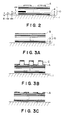
- Figure 2 shows a reflection type mask according to a first embodiment of the present invention.
- the mask of this embodiment is suitable for use with a radiation of wavelength 12.4 nm (124 ⁇ ) as the exposing radiation.
- the mask includes a substrate 1 which may be formed by a silicon single crystal plate having a ground surface having surface roughness not larger than 1.0 nm (10 ⁇ )(rms).
- a substrate 1 which may be formed by a silicon single crystal plate having a ground surface having surface roughness not larger than 1.0 nm (10 ⁇ )(rms).
- a large number of layers is formed, although only some of which are shown in the drawing for ease in illustration.
- the first type layers and the second type layers are formed alternately, as illustrated, to provide a reflective base portion 10 of multilayered structure.
- the first type layers and the second type layers were made by sputtering deposition after a super high vacuum pressure not greater than 1x10 -6 Pa was achieved and with an argon pressure of 5x10 -1 Pa.
- Each of the first type layers had a thickness of 2.98 nm (29.8 ⁇ ) while each of the second type layers had a thickness of 3.39 nm (33.9 ⁇ ).
- Forty-one layers comprising the first type layers of a number twenty-one and the second type layers of a number twenty were formed on the substrate.
- a surface layer of carbon (C) was formed with a thickness 1.0 nm (10 ⁇ ) upon the top layer as a protection film B ( Figure 3A), whereby a reflective base portion of multilayered structure was obtained.
- the first type layers have a refractive index whose real number portion is smaller while the second type layers have a refractive index whose real number portion is larger. This is because, as will be readily understood from the Fresnel reflection theory, such a material whose refractive index has a large difference from that of an ambience, such as an air, should preferably be used as the material of the final layer.
- each layer can be determined in accordance with the aforementioned Bragg diffraction formula and on the basis of the refractive index of each material and the wavelength of the radiation to be used.
- the thickness can be determined as follows:
- the thickness of each layer can be determined.
- n 1 0.91 + 6.8 x 10 -3 i
- the thicknesses can be determined as follows: d 1 ⁇ 2.98 nm (29.8 ⁇ ) d 2 ⁇ 3.39 nm (33.9 ⁇ )
- a resist layer of PMMA was formed on the reflective base portion with a thickness 0.5 ⁇ m .
- the resist layer was patterned with 1.75 ⁇ m line-and-space.
- gold (linear expansion coefficient: 1.42x10 -5 /deg and heat conductivity: 3.16 J/cm.s.deg) was deposited on the resist layer, by electron beam deposition and with a thickness of 0.1 ⁇ m ( Figure 3B).
- gold is a material that can absorb soft X-rays.
- the PMMA material was removed, whereby a gold pattern A was obtained on the multilayered film (see Figure 3C).
- a ground silicon single crystal plate 1 was used.
- each of the first type layer and the second type layer can be determined in accordance with equation (1) related to the Bragg diffraction, as described hereinbefore.
- PMMA layer of a thickness 0.5 ⁇ m was formed on the thus obtained reflective base portion of multilayered structure, and the PMMA layer was patterned by electron-beam patterning process.
- tantalum (Ta) linear expansion coefficient: 6.3x10 -6 /deg and heat conductivity: 0.575 J/cm.s.deg
- the PMMA material was removed, such that a tantalum pattern was obtained on the multilayered film.
- a ground silicon single crystal plate was used.
- a super high vacuum pressure not greater than 1 x 10 -6 Pa forty-one layers (twenty-one layers of Pd and twenty layers of Si) were formed on the substrate by electron-beam deposition, with respective thicknesses 2.11 nm (21.1 ⁇ ) and 4.03 nm (40.3 ⁇ ).
- a layer of carbon (C) of a thickness 1.0 nm (10 ⁇ ) was formed thereupon as a protection film.
- the first type layers have a refractive index whose real number portion is smaller and the second type layers have a refractive index whose real number portion is larger.
- a PMMA layer of a thickness 0.5 ⁇ m was formed on the thus obtained reflective base portion of multilayered structure, and, then, the PMMA layer was patterned by electron-beam patterning process.
- silicon (Si) linear expansion coefficient: 2.6x10 -6 /deg and heat conductivity: 1.49J/cm.s.deg) which is a soft X-ray absorbing material was deposited by electron-beam deposition to a thickness of 0.1 um.
- the PMMA material was removed, with the result that a silicon pattern was obtained on the multilayered film.
- a silicon single crystal plate is used as the substrate
- the material is not limited thereto.
- a glass plate, a fused silica plate, a silicon carbide plate or otherwise may be used, provided that its surface is made sufficiently smooth, by grinding, as compared with the wavelength of radiation to be used.
- Figure 4 shows a reflection type mask according to a second embodiment of the present invention.
- Figure 5 is a schematic illustration for explaining a problem which can be solved by the present embodiment.
- denoted at 21 are non-reflective elements patterned on a reflective base portion of a multilayered film structure.
- Denoted at 20 are reflecting portions, and denoted at 25 is a substrate.
- the half shade 23 can be reduced by reducing the thickness (height) of the non-reflective pattern 21. Actually, however, to do so might be very difficult since an ordinary X-ray absorbing material does not have a high X-ray absorbing efficiency so that a substantial thickness is required for the material to provide a sufficient X-ray absorbing function.
- the non-reflective pattern is provided by a multilayered film structure which is arranged so that, by the interference effect, the light reflected from the upper surface of a first layer (such as ) and the light reflected from the upper surface of a second layer (such as ) act upon one another to mutually weaken the intensity.
- the layer thickness is determined for this purpose.
- the non-reflective portion D can function as an anti-reflection film.
- the non-reflective portion D of the multilayered structure can be reduced in thickness significantly while retaining high non-reflection efficiency, as compared with that of a non-reflective portion simply made of an X-ray absorbing material.
- the mask of the present embodiment has a reflective base portion 10 comprising a multilayered film showing reflectivity to soft X-rays or otherwise.
- the reflective portion 10 is formed on a non-reflective flat substrate 1 made of a material absorbing soft X-rays or otherwise.
- the non-reflective portion D comprises a multilayered film and is formed on the reflective portion 10, to thereby provide a predetermined pattern.
- the reflective portion 10 is formed by layering two different materials having different optical constants to provide first type layers 2, 4, 6, ... and second type layers 3, 5, 7, ... in an alternate fashion.
- the thicknesses d 1 , d 2 , d 3 , d 4 , ... of the two types of layers are not less than 1.0 nm (10 ⁇ ).
- the thickness of each layer is less than 1.0 nm (10 ⁇ )
- the reflection factor can be improved.
- the number of layers may preferably be not greater than two hundred.
- the non-reflective portion D comprises alternately provided layers made of the different materials and constitutes an anti-reflection film to the reflective portion 10.
- a reflection type mask has an intensity ratio of 2:1, preferably 10:1, in respect to the intensities of the soft X-rays or otherwise reflected by the reflective portion 10 and the non-reflective portion D, respectively.
- the anti-reflection film may preferably be formed by two or more layers, although the number intimately depends upon the wavelength range to be used.
- the soft X-rays or otherwise of a wavelength near 10.0 nm (100 ⁇ ) for example, the provision of three or more layers is preferable.
- each layer of the anti-reflection film has a thickness approximately of an order of ⁇ /4n wherein ⁇ is the wavelength and n is the refractive index.
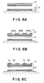
- a silicon single crystal plate which has been ground to a surface roughness not greater than 1.0 nm (10 ⁇ ) (rms) was used as the substrate 1 ( Figure 6A).
- a super high vacuum pressure not greater than 1x10 -6 Pa was achieved, forty-one layers (twenty-one layers of Mo and twenty layers of Si) were formed on the substrates with a thickness 2.7 nm (27 ⁇ ) (for each first type layer Mo) and a thickness 38.9 nm (38.9 ⁇ ) (for each second type layer Si), by sputtering deposition while maintaining an argon pressure of 5x10 -2 Pa.
- the reflective base portion 10 was formed.
- a carbon layer was formed on the reflective portion 10 as a protection film B.
- the thicknesses were determined in the same manner as in the examples described hereinbefore.
- the selection of materials is made so that the first type layers (Mo) have a refractive index whose real number portion is smaller while the second type layers (Si) have a refractive index whose real number portion is larger.
- a layer of a resist material PMMA was formed on the reflective portion 10 with a thickness 0.5 micron. Then, by electron beam patterning, the PMMA layer was patterned with 1.75 ⁇ m line-and-space. As a result, a patterned resist layer of PMMA was obtained.
- silicon (Si) and molybdenum (Mo) were alternately deposited by sputtering deposition to form thirteen alternate layers of Si and Mo having thicknesses 7.1, 3.7, 3.1, ..., 3.6, 3.2, 3.6 and 3.3 nm (71, 37, 31, ..., 36, 32, 36 and 33 ⁇ ).
- the conditions of the sputtering deposition were the same as those at the time of manufacture of the reflective portion 10.
- the thicknesses are those that satisfy " ⁇ /4n" described hereinbefore.
- the thickness of the non-reflective portion 31 as a whole was 48.0 nm (480 ⁇ ).
- reference samples were also placed in a deposition apparatus. At the time of formation of the reflective portion, three reference samples were set and, at the time of formation of the non-reflective portion, one of them was set again. This was done to allow measurement of the reflection factor of a reflective portion and the reflection factor of a reflective portion having a non-reflective portion formed thereon. By the measurement with a wavelength 13.0 nm (130 ⁇ ) and with an angle of incidence of 10 degrees, it was confirmed that the former has a reflection factor of 52 % and the latter has a reflection factor of 28 %.
- the mask of this example may be used with a wavelength of 12.4 nm (124 ⁇ ).
- the thicknesses were determined in the same manner as the foregoing example. Subsequently, the resist material PMMA was removed, with the result that a mask having a reflective portion of multilayered film structure and a non-reflective portion formed on the reflective portion and having a multilayered film structure, was obtained.
- the thickness of the non-reflective portion as a whole was 31.8 nm (318 ⁇ ).
- reference samples were prepared so as to confirm the anti-reflection effect of the non-reflective portion.
- a reflection factor of 52% was measured with a wavelength 13.0 nm (130 ⁇ ) and an angle of incidence of 1.0 degree.
- a reflection factor 3.2 % was measured for the reflective portion.
- an absorptive element provided by depositing tungsten on the surface of the reflective portion of the sample with a thickness 72.0 nm (720 ⁇ a reflection factor of 4.7 % was measured.
- the absorptive element must has a thickness twice or more greater than the thickness of the non-reflective portion of multilayered film structure.
- the protection film provided on the upper surface of the reflective portion is preferably made by a carbon layer of a thickness not greater than than 10.0 nm (100 ⁇ ). However, such a protection film may be omitted.
- the multilayered structure of the reflective portion is formed by alternately layering two different materials, three or more materials may be used and layered in sequence.
- a silicon single crystal plate is used in the present embodiment as a substrate, the material is not limited thereto.
- a glass plate, a fused silica plate, a silicon carbide plate or otherwise may be used, provided that its surface is made sufficiently smooth, by grinding, as compared with the wavelength to be used.
- Figure 7 shows the structure of a reflection type mask according to a third embodiment of the present invention.
- a mask pattern is formed by selectively irradiating a reflective base portion of multilayered film structure with a particular radiation beam so as to change the physical and/or chemical characteristics of the reflective portion to thereby destroy the regularity of the multilayered structure in the portion irradiated by the radiation beam.
- a ground quartz plate having a surface roughness not greater than 0.2 nm (2 ⁇ ) (rms) was used as a substrate 1.
- first type layers Forty-one layers (twenty-one layers of Mo and twenty layers of Si) were formed in an alternately layered fashion to provide first type layers 2, 4, 6, ... made of Mo and second type layers 3, 5, 7, ... made of Si.
- the thickness of each of the first type layers (Mo) was 2.7 nm (27 ⁇ ) and the thickness of each of the second type layers (Si) was 3.6 nm (36 ⁇ ). The thickness was determined similarly as in the examples described hereinbefore.
- the selection of materials for the first and second layers has been made so that the first type layers (Mo) have a refractive index whose real number portion is smaller while the second type layers (Si) have a refractive index whose real number portion is larger.
- the thus formed reflective portion comprising a multilayered film was irradiated with a focused silicon ion beam having a focused beam diameter of 0.1 ⁇ m under an acceleration voltage 200 Kev.
- a focused silicon ion beam having a focused beam diameter of 0.1 ⁇ m under an acceleration voltage 200 Kev.
- the regularity of the layered structure of the part of the reflective portion 10 irradiated with the ion beam was destroyed so that the irradiated part of the reflective portion 10 lost the function of a "reflecting surface".
- a plurality of non-reflective portions 22 were formed in the reflective portion 10 and a pattern of 0.8 ⁇ m line-and-space was obtained.
- the beam current was 100 PA.
- the thus obtained reflective portion of multilayered film structure was selectively irradiated with a focused argon laser beam with an output power of 5 W.
- the regularity of the layered structure of the part of the reflective portion irradiated with the laser beam was destroyed so that the irradiated part lost the function as a "reflecting surface".
- non-reflective portions 22 formed in the reflective portion and a pattern of 1 ⁇ m line-and-space was obtained.
- the means for destroying the regularity of the layered structure is not limited to the converging ion-beam scanning apparatus or the use of a laser beam.
- an electron beam may be used. It is a further alternative that a resist pattern is first formed on a multilayered film and a glass plasma is used to destroy the regularity of the layered structure, the resist material being thereafter removed.
- a reflection type mask will be used, in many cases, with an intense X-ray source such as, for example, a light source means using a synchrotron emission light source.
- an intense X-ray source such as, for example, a light source means using a synchrotron emission light source.
- a temperature increase due to the absorption of a radiation energy by the mask.
- the thermal expansion due to the temperature increase will cause shift of the position of a pattern on the mask surface or distortion of the mask pattern. This is a very serious problem in the reproduction of patterns having a submicrometre linewidth.
- a bulk material may be used as the substrate.
- the mask itself can be cooled by water or otherwise. Therefore, it is possible to diminish, remarkably, the adverse effect of the temperature increase in the mask.
- a material (examples of which will be described later) having a high heat conductivity as for the substrate and the multilayered film, the heat can be radiated efficiently with an advantageous effect of prevention of the temperature increase.
- a material (examples of which will be described later) having a small linear expansion coefficient may be used as the substrate and the multilayered film. This is effective to suppress the occurrence of distortion due to the temperature increase.
- the material of the substrate which may be used preferably, there are silicon carbide, aluminum nitride, silicon nitride of ceramics series, for example. Particularly, the silicon carbide is preferable because it has a very large heat conductivity (of an order of 100 w/mK).
- the material usable in the multilayered film as one type layer there are transition metal such as tungsten, tantalum, molybdenum, rhodium, ruthenium or otherwise, carbide, nitride, silicide, boride, oxide or otherwise of any one of the aforementioned transition metals.
- the material which may be used as the other type layer there are silicon, beryllium, carbon, boron, composite of these materials (e.g. silicon carbide, boron carbide), oxide, nitride or otherwise of these materials such as silicon oxide, silicon nitride and so on.
- the silicon carbide has a linear expansion coefficient of not greater than 4.5x10 -6 K -1 and the tungsten has a linear expansion coeffcient of not greater than 4.5x10 -6 K -1 , so that they are preferble.
- molybdenum usable as the material of the reflective portion has a linear expansion coefficient of not greater than 4.8x10 -6 K -1 , and therefore molybdenum is a preferable material.
- a material having a linear expansion coefficient not greater than 1x10 -5 /K and a heat conductivity not less than 20 w/mK is preferable to use as for the material of the substrate, the material of the reflective portion and the material of the non-reflective portion.
- the manufacture of the multilayered film is not limited to use of the ion-beam sputtering method or the electron-beam deposition method using a super high vacuum.
- Other thin film manufacturing techniques such as double-electrode sputtering method, organic metal chemical vapour deposition method (called "MOCVD method"), etc., may be adopted.
- the mask may be formed so that the substrate thereof has a curved surface such as, for example, a spherical surface, an aspherical surface, an asymmetrically curved surface, etc.
Claims (10)
- Reflexionsmaske (Mo), die in einer Belichtungsapparatur mit einem optischen Projektionssystem verwendet werden kann, das eine Vielzahl an Spiegeln (M1,M2,M3) aufweist, die zwischen der Maske und einem Werkstück (W) angeordnet sind, um mittels weicher Röntgenstrahlung oder Vakuum-UV-Strahlung ein Maskenmuster auf das Werkstück zu übertragen, dadurch gekennzeichnet, daß
die Maske eine reflektierende Oberfläche (10;10;24), die von einem mehrschichtigen Film (2-5;2-5;2-5) bereitgestellt wird, und einen nichtreflektierenden Bereich (A;D;21;22) aufweist, der in oder auf der reflektierenden Oberfläche bereitgestellt wird, um das Muster festzulegen, wobei der nicht-reflektierende Bereich (A;D;21;22) eine Schwächung der weichen Röntgenstrahlung oder der Vakuum-UV-Strahlung bewirkt. - Maske nach Anspruch 1,
dadurch gekennzeichnet, daß
der nicht-reflektierende Bereich (A;D;21) ein absorbierendes Material umfaßt, das auf dem mehrschichtigen Film (2-5;2-5;24) aufgebracht ist. - Maske nach Anspruch 1,
dadurch gekennzeichnet, daß
der nicht-reflektierende Bereich (22) ein ungeordneter Bereich (22) des mehrschichtigen Films (2-5) ist. - Reflexionsmaske nach Anspruch 1,
dadurch gekennzeichnet, daß
das absorbierende Material des nicht-reflektierenden Bereichs (A;D;21;22) einen linearen Ausdehnungskoeffizienten, der nicht größer als 5 x 10⁻⁵ deg-1 ist, und eine Wärmeleitfähigkeit von nicht kleiner als 0,1 J/cm.s.deg aufweist. - Reflexionsmaske nach Anspruch 1,
dadurch gekennzeichnet, daß
der mehrschichtige Film (2-5) aus alternierenden Schichten (2,3,4,5) aus jeweils unterschiedlichen Materialien mit unterschiedlichen optischen Konstanten gebildet ist. - Reflexionsmaske nach Anspruch 5,
dadurch gekennzeichnet, daß
der mehrschichtige Film erste Schichten (2,4,...) mit einem Brechungsindex, dessen Realteil kleiner ist, und zweite, alternierende Schichten (3,5,...) mit einem Brechungsindex, dessen Realteil größer ist, aufweist, wobei sich die ersten und zweiten Schichten (2-5) weiter weg von beziehungsweise näher an der Oberfläche der Reflexionsmaske befinden. - Belichtungsverfahren zum Übertragen eines Musters einer Reflexionsmaske auf ein Werkstück mittels weicher Röntgenstrahlung oder Vakuum-UV-Strahlung, wobei das Verfahren die nachstehenden Schritte umfaßt:Bereitstellung einer Reflexionsmaske (Mo) nach einem der vorstehenden Ansprüche 1 bis 6; undBestrahlen der Maske (Mo) mit der Strahlung und Aussetzen des Werkstücks (W) der von der Maske (Mo) reflektierten Strahlung mittels eines optisches Projektionssystem, das eine Vielzahl an Spiegeln (M1, M2, M3) aufweist, wodurch das Muster der Maske (Mo) auf das Werkstück (W) übertragen wird.
- Verfahren nach Anspruch 7, in dem das Muster der Maske (Mo), das auf das Werkstück projeziert wird, einen verkleinerten Maßstab aufweist.
- Belichtungsgerät zum Übertragen eines Musters einer Reflexionsmaske mittels weicher Röntgenstrahlung oder Vakuum-UV-Strahlung auf ein Werkstück, wobei das Gerät die nachstehenden Bestandteile umfaßt:eine Halteeinrichtung zum Halten der Reflexionsmaske (Mo);eine Reflexionsmaske (Mo), die von der Halteeinrichtung gehalten wird, wobei es sich um eine Maske (Mo) nach einem der vorstehenden Ansprüche 1 bis 6 handelt; undeine optische Einrichtung zum Bestrahlen der Maske (Mo) mit der Strahlung und zum Belichten des Werkstücks (W) mit der von der Maske (Mo) reflektierten Strahlung, wobei die optische Einrichtung ein optisches Projektionssystem mit einer Vielzahl an Spiegeln (M1,M2,M3) zum Projezieren des Musters der Maske auf das Werkstück umfaßt, wodurch das Muster der Maske (Mo) auf das Werkstück (W) übertragen wird.
- Gerät nach Anspruch 9, das ferner ein optisches System zum Projezieren des Musters der Maske (Mo) in verkleinertem Maßstab auf das Werkstück umfaßt.
Applications Claiming Priority (12)
| Application Number | Priority Date | Filing Date | Title |
|---|---|---|---|
| JP33523/87 | 1987-02-18 | ||
| JP3352387A JPH0727198B2 (ja) | 1987-02-18 | 1987-02-18 | 多層膜反射型マスク |
| JP335222/87 | 1987-12-29 | ||
| JP335223/87 | 1987-12-29 | ||
| JP33522287A JP2545905B2 (ja) | 1987-12-29 | 1987-12-29 | 反射型マスクならびにこれを用いた露光方法 |
| JP62335220A JPH01175734A (ja) | 1987-12-29 | 1987-12-29 | 反射型マスク及びその製造方法 |
| JP335221/87 | 1987-12-29 | ||
| JP33522387A JP2546312B2 (ja) | 1987-12-29 | 1987-12-29 | 反射型マスクおよび該反射型マスクを用いた露光装置と露光方法 |
| JP62335221A JPH01175735A (ja) | 1987-12-29 | 1987-12-29 | 反射型マスク及びその製造方法 |
| JP335220/87 | 1987-12-29 | ||
| JP1213688A JP2615741B2 (ja) | 1988-01-22 | 1988-01-22 | 反射型マスクならびにこれを用いた露光装置と露光方法 |
| JP12136/87 | 1988-01-22 |
Publications (3)
| Publication Number | Publication Date |
|---|---|
| EP0279670A2 EP0279670A2 (de) | 1988-08-24 |
| EP0279670A3 EP0279670A3 (de) | 1990-03-14 |
| EP0279670B1 true EP0279670B1 (de) | 1997-10-29 |
Family
ID=27548393
Family Applications (1)
| Application Number | Title | Priority Date | Filing Date |
|---|---|---|---|
| EP88301367A Expired - Lifetime EP0279670B1 (de) | 1987-02-18 | 1988-02-18 | Reflexionsmaske |
Country Status (3)
| Country | Link |
|---|---|
| US (1) | US5052033A (de) |
| EP (1) | EP0279670B1 (de) |
| DE (1) | DE3856054T2 (de) |
Families Citing this family (62)
| Publication number | Priority date | Publication date | Assignee | Title |
|---|---|---|---|---|
| US4923772A (en) * | 1986-10-29 | 1990-05-08 | Kirch Steven J | High energy laser mask and method of making same |
| JPH0797216B2 (ja) * | 1986-10-29 | 1995-10-18 | インタ−ナショナル・ビジネス・マシ−ンズ・コ−ポレ−ション | マスクの製造方法 |
| FR2653234A1 (fr) * | 1989-10-13 | 1991-04-19 | Philips Electronique Lab | Dispositif du type miroir dans le domaine des rayons x-uv. |
| US5182763A (en) * | 1989-12-28 | 1993-01-26 | Canon Kabushiki Kaisha | Reflection device |
| JPH03266842A (ja) * | 1990-03-16 | 1991-11-27 | Fujitsu Ltd | 反射型ホトリソグラフィ方法、反射型ホトリソグラフィ装置および反射型ホトマスク |
| JP2599513B2 (ja) * | 1990-06-25 | 1997-04-09 | インターナショナル・ビジネス・マシーンズ・コーポレイション | アブレーション・マスク |
| JP2979667B2 (ja) * | 1991-01-23 | 1999-11-15 | 株式会社ニコン | 反射型のx線露光用マスク |
| JP3025545B2 (ja) * | 1991-03-18 | 2000-03-27 | キヤノン株式会社 | X線リソグラフィ用マスクおよびx線リソグラフィ露光装置 |
| US5335256A (en) * | 1991-03-18 | 1994-08-02 | Canon Kabushiki Kaisha | Semiconductor substrate including a single or multi-layer film having different densities in the thickness direction |
| JP3047541B2 (ja) * | 1991-08-22 | 2000-05-29 | 株式会社日立製作所 | 反射型マスクおよび欠陥修正方法 |
| DE69220868T2 (de) * | 1991-09-07 | 1997-11-06 | Canon Kk | System zur Stabilisierung der Formen von optischen Elementen, Belichtungsvorrichtung unter Verwendung dieses Systems und Verfahren zur Herstellung von Halbleitervorrichtungen |
| US5485497A (en) * | 1991-11-12 | 1996-01-16 | Hitachi, Ltd. | Optical element and projection exposure apparatus employing the same |
| JP3012069B2 (ja) * | 1991-12-04 | 2000-02-21 | キヤノン株式会社 | X線露光用マスク構造体及びこれを用いたx線露光装置 |
| JPH07117605B2 (ja) * | 1992-03-13 | 1995-12-18 | 日本ピラー工業株式会社 | 回折格子 |
| JPH05281704A (ja) * | 1992-04-02 | 1993-10-29 | Nec Corp | 半導体集積回路用ホトマスク |
| US5304437A (en) * | 1992-04-03 | 1994-04-19 | At&T Bell Laboratories | Mask for x-ray pattern delineation |
| JPH0689848A (ja) * | 1992-07-20 | 1994-03-29 | Canon Inc | X線マスク構造体の作製方法及び該作製方法により作製されたx線マスク構造体、並びに該x線マスク構造体を用い作製されたデバイス |
| US5307395A (en) * | 1992-09-30 | 1994-04-26 | The United States Of America As Represented By The Secretary Of The Navy | Low-damage multilayer mirror for the soft X-ray region |
| JP3219502B2 (ja) * | 1992-12-01 | 2001-10-15 | キヤノン株式会社 | 反射型マスクとその製造方法、並びに露光装置と半導体デバイス製造方法 |
| US5356662A (en) * | 1993-01-05 | 1994-10-18 | At&T Bell Laboratories | Method for repairing an optical element which includes a multilayer coating |
| JPH0772318A (ja) * | 1993-04-28 | 1995-03-17 | Canon Inc | 反射装置とこれを用いた照明装置や露光装置、並びにデバイス製造方法 |
| JPH07240364A (ja) * | 1994-03-02 | 1995-09-12 | Canon Inc | 反射型マスク、その製造方法及び該マスクを用いた露光装置 |
| US5827622A (en) * | 1995-11-02 | 1998-10-27 | International Business Machines Corporation | Reflective lithographic mask |
| DE69702641T2 (de) * | 1996-03-07 | 2001-04-05 | Koninkl Philips Electronics Nv | Belichtungssystem und belichtungsgerät für uv-lithographie |
| JP3814359B2 (ja) | 1996-03-12 | 2006-08-30 | キヤノン株式会社 | X線投影露光装置及びデバイス製造方法 |
| US6317479B1 (en) * | 1996-05-17 | 2001-11-13 | Canon Kabushiki Kaisha | X-ray mask, and exposure method and apparatus using the same |
| JP3774522B2 (ja) * | 1996-12-24 | 2006-05-17 | キヤノン株式会社 | 回折光学素子及びそれを有する光学機器 |
| US5978441A (en) * | 1997-12-01 | 1999-11-02 | Advanced Micro Devices, Inc. | Extreme ultraviolet lithography mask blank and manufacturing method therefor |
| WO2000003341A1 (en) * | 1998-07-10 | 2000-01-20 | Ball Semiconductor, Inc. | A method and system for generating a flat mask onto a three-dimensional surface |
| US6316150B1 (en) | 1998-08-24 | 2001-11-13 | Euv Llc | Low thermal distortion extreme-UV lithography reticle |
| AU5932500A (en) | 1999-07-22 | 2001-02-13 | Corning Incorporated | Extreme ultraviolet soft x-ray projection lithographic method and mask devices |
| US6596465B1 (en) | 1999-10-08 | 2003-07-22 | Motorola, Inc. | Method of manufacturing a semiconductor component |
| KR100446126B1 (ko) * | 1999-11-29 | 2004-08-30 | 토호쿠 테크노 아르크 코포레이션 리미티드 | 다층막 반사경 등의 광학 소자, 그 제조방법 및 그를이용한 장치 |
| DE10016008A1 (de) * | 2000-03-31 | 2001-10-11 | Zeiss Carl | Villagensystem und dessen Herstellung |
| US20070281109A1 (en) * | 2000-03-31 | 2007-12-06 | Carl Zeiss Smt Ag | Multilayer system with protecting layer system and production method |
| US7261957B2 (en) * | 2000-03-31 | 2007-08-28 | Carl Zeiss Smt Ag | Multilayer system with protecting layer system and production method |
| US6625251B2 (en) * | 2000-09-22 | 2003-09-23 | Ntt Advanced Technology Corporation | Laser plasma x-ray generation apparatus |
| US6821682B1 (en) * | 2000-09-26 | 2004-11-23 | The Euv Llc | Repair of localized defects in multilayer-coated reticle blanks for extreme ultraviolet lithography |
| US6776006B2 (en) | 2000-10-13 | 2004-08-17 | Corning Incorporated | Method to avoid striae in EUV lithography mirrors |
| JP2002245947A (ja) * | 2000-12-15 | 2002-08-30 | Canon Inc | 細線を有する基板及びその製造方法及び電子源基板及び画像表示装置 |
| US6635391B2 (en) * | 2000-12-28 | 2003-10-21 | The Regents Of The University Of California | Method for fabricating reticles for EUV lithography without the use of a patterned absorber |
| JP2002299228A (ja) * | 2001-04-03 | 2002-10-11 | Nikon Corp | レチクル、それを用いた露光装置及び露光方法 |
| DE10123768C2 (de) * | 2001-05-16 | 2003-04-30 | Infineon Technologies Ag | Verfahren zur Herstellung einer lithographischen Reflexionsmaske insbesondere für die Strukturierung eines Halbleiterwafers sowie Reflexionsmaske |
| US7053988B2 (en) | 2001-05-22 | 2006-05-30 | Carl Zeiss Smt Ag. | Optically polarizing retardation arrangement, and microlithography projection exposure machine |
| US6967168B2 (en) * | 2001-06-29 | 2005-11-22 | The Euv Limited Liability Corporation | Method to repair localized amplitude defects in a EUV lithography mask blank |
| US6673520B2 (en) | 2001-08-24 | 2004-01-06 | Motorola, Inc. | Method of making an integrated circuit using a reflective mask |
| US6653053B2 (en) | 2001-08-27 | 2003-11-25 | Motorola, Inc. | Method of forming a pattern on a semiconductor wafer using an attenuated phase shifting reflective mask |
| DE10155112B4 (de) * | 2001-11-09 | 2006-02-02 | Infineon Technologies Ag | Reflexionsmaske für die EUV-Lithographie und Herstellungsverfahren dafür |
| US6986971B2 (en) * | 2002-11-08 | 2006-01-17 | Freescale Semiconductor, Inc. | Reflective mask useful for transferring a pattern using extreme ultraviolet (EUV) radiation and method of making the same |
| DE10259331B4 (de) * | 2002-12-18 | 2005-02-10 | Infineon Technologies Ag | Herstellungsverfahren für eine Photomaske für eine integrierte Schaltung und entsprechende Photomaske |
| DE10261137A1 (de) * | 2002-12-21 | 2004-07-15 | Carl Zeiss Smt Ag | Projektionsoptik für die Lithographie und Spiegel für eine solche |
| US6875546B2 (en) * | 2003-03-03 | 2005-04-05 | Freescale Semiconductor, Inc. | Method of patterning photoresist on a wafer using an attenuated phase shift mask |
| US7026076B2 (en) * | 2003-03-03 | 2006-04-11 | Freescale Semiconductor, Inc. | Method of patterning photoresist on a wafer using a reflective mask with a multi-layer ARC |
| US6986974B2 (en) * | 2003-10-16 | 2006-01-17 | Freescale Semiconductor, Inc. | Attenuated phase shift mask for extreme ultraviolet lithography and method therefore |
| JP2005302963A (ja) * | 2004-04-09 | 2005-10-27 | Canon Inc | 露光装置 |
| JP2006049837A (ja) * | 2004-06-30 | 2006-02-16 | Canon Inc | 厚膜部材パターンの製造方法 |
| US7485410B2 (en) * | 2004-06-30 | 2009-02-03 | Canon Kabushiki Kaisha | Method of manufacturing thick dielectric pattern and method of manufacturing image displaying apparatus |
| KR100607201B1 (ko) * | 2005-01-04 | 2006-08-01 | 삼성전자주식회사 | 극자외선 리소그래피 공정에서 웨이퍼 상의 임계 치수편차를 보정하는 방법 |
| JP5018787B2 (ja) * | 2006-12-27 | 2012-09-05 | 旭硝子株式会社 | Euvリソグラフィ用反射型マスクブランク |
| WO2008093534A1 (ja) * | 2007-01-31 | 2008-08-07 | Asahi Glass Company, Limited | Euvリソグラフィ用反射型マスクブランク |
| CN102132209B (zh) | 2008-08-21 | 2014-07-16 | Asml控股股份有限公司 | 具有高热传导率的euv掩模版基底 |
| US9195132B2 (en) * | 2014-01-30 | 2015-11-24 | Globalfoundries Inc. | Mask structures and methods of manufacturing |
Family Cites Families (6)
| Publication number | Priority date | Publication date | Assignee | Title |
|---|---|---|---|---|
| JPS57106031A (en) * | 1980-12-23 | 1982-07-01 | Toshiba Corp | Transferring device for fine pattern |
| US4693933A (en) * | 1983-06-06 | 1987-09-15 | Ovonic Synthetic Materials Company, Inc. | X-ray dispersive and reflective structures and method of making the structures |
| JPS60173551A (ja) * | 1984-02-20 | 1985-09-06 | Hideki Matsumura | X線など光線の反射投影によるパタ−ン転写法 |
| WO1987006028A2 (en) * | 1986-03-28 | 1987-10-08 | Shimadzu Corporation | X-ray reflective mask and system for image formation with use of the same |
| EP0947882B1 (de) * | 1986-07-11 | 2006-03-29 | Canon Kabushiki Kaisha | Verkleinerndes Projektionsbelichtungssystem des Reflexionstyps für Röntgenstrahlung |
| US4923772A (en) * | 1986-10-29 | 1990-05-08 | Kirch Steven J | High energy laser mask and method of making same |
-
1988
- 1988-02-18 DE DE3856054T patent/DE3856054T2/de not_active Expired - Lifetime
- 1988-02-18 EP EP88301367A patent/EP0279670B1/de not_active Expired - Lifetime
-
1990
- 1990-12-28 US US07/633,181 patent/US5052033A/en not_active Expired - Lifetime
Also Published As
| Publication number | Publication date |
|---|---|
| EP0279670A2 (de) | 1988-08-24 |
| DE3856054D1 (de) | 1997-12-04 |
| EP0279670A3 (de) | 1990-03-14 |
| DE3856054T2 (de) | 1998-03-19 |
| US5052033A (en) | 1991-09-24 |
Similar Documents
| Publication | Publication Date | Title |
|---|---|---|
| EP0279670B1 (de) | Reflexionsmaske | |
| US11754917B2 (en) | Extreme ultraviolet mask blank with multilayer absorber and method of manufacture | |
| EP0708367B1 (de) | Gerät zur Darstellung von Mustern zum Einsatz im extremen UV-Bereich | |
| JP3078163B2 (ja) | リソグラフィ用反射型マスクおよび縮小投影露光装置 | |
| US6833223B2 (en) | Multilayer-film reflective mirrors and optical systems comprising same | |
| KR100589240B1 (ko) | Euv 광학 요소의 캡핑 층 | |
| US6048652A (en) | Backside polish EUV mask and method of manufacture | |
| JP3219502B2 (ja) | 反射型マスクとその製造方法、並びに露光装置と半導体デバイス製造方法 | |
| CN110501769A (zh) | 用于光刻设备内的膜和包括这种膜的光刻设备 | |
| JPH11506876A (ja) | 紫外線リトグラフィー用の結像システム及び装置 | |
| CN1312531C (zh) | 光刻掩模制造 | |
| JP2545905B2 (ja) | 反射型マスクならびにこれを用いた露光方法 | |
| JPH0727198B2 (ja) | 多層膜反射型マスク | |
| JPH0868897A (ja) | 反射鏡およびその製造方法 | |
| US6830851B2 (en) | Photolithographic mask fabrication | |
| JP2006194764A (ja) | 多層膜反射鏡および露光装置 | |
| JPH10339799A (ja) | 反射鏡及びその製造方法 | |
| JP2615741B2 (ja) | 反射型マスクならびにこれを用いた露光装置と露光方法 | |
| JPH05144710A (ja) | 光学素子及びその製造方法 | |
| US8906582B2 (en) | Blank masks for extreme ultra violet lithography, methods of fabricating the same, and methods of correcting registration errors thereof | |
| JP7295260B2 (ja) | 多層吸収体を備えた極紫外線マスクブランクおよび製造方法 | |
| US11815803B2 (en) | Multilayer extreme ultraviolet reflector materials | |
| JP2675263B2 (ja) | 反射型マスクを用いた露光装置および露光方法 | |
| JPH01175734A (ja) | 反射型マスク及びその製造方法 | |
| JP2615741C (de) |
Legal Events
| Date | Code | Title | Description |
|---|---|---|---|
| PUAI | Public reference made under article 153(3) epc to a published international application that has entered the european phase |
Free format text: ORIGINAL CODE: 0009012 |
|
| AK | Designated contracting states |
Kind code of ref document: A2 Designated state(s): DE FR GB |
|
| PUAL | Search report despatched |
Free format text: ORIGINAL CODE: 0009013 |
|
| AK | Designated contracting states |
Kind code of ref document: A3 Designated state(s): DE FR GB |
|
| 17P | Request for examination filed |
Effective date: 19900730 |
|
| 17Q | First examination report despatched |
Effective date: 19930322 |
|
| GRAG | Despatch of communication of intention to grant |
Free format text: ORIGINAL CODE: EPIDOS AGRA |
|
| GRAH | Despatch of communication of intention to grant a patent |
Free format text: ORIGINAL CODE: EPIDOS IGRA |
|
| GRAH | Despatch of communication of intention to grant a patent |
Free format text: ORIGINAL CODE: EPIDOS IGRA |
|
| GRAA | (expected) grant |
Free format text: ORIGINAL CODE: 0009210 |
|
| AK | Designated contracting states |
Kind code of ref document: B1 Designated state(s): DE FR GB |
|
| REF | Corresponds to: |
Ref document number: 3856054 Country of ref document: DE Date of ref document: 19971204 |
|
| ET | Fr: translation filed | ||
| PLBE | No opposition filed within time limit |
Free format text: ORIGINAL CODE: 0009261 |
|
| STAA | Information on the status of an ep patent application or granted ep patent |
Free format text: STATUS: NO OPPOSITION FILED WITHIN TIME LIMIT |
|
| 26N | No opposition filed | ||
| REG | Reference to a national code |
Ref country code: GB Ref legal event code: IF02 |
|
| PGFP | Annual fee paid to national office [announced via postgrant information from national office to epo] |
Ref country code: GB Payment date: 20070214 Year of fee payment: 20 |
|
| PGFP | Annual fee paid to national office [announced via postgrant information from national office to epo] |
Ref country code: DE Payment date: 20070418 Year of fee payment: 20 |
|
| REG | Reference to a national code |
Ref country code: GB Ref legal event code: PE20 |
|
| PGFP | Annual fee paid to national office [announced via postgrant information from national office to epo] |
Ref country code: FR Payment date: 20070221 Year of fee payment: 20 |
|
| PG25 | Lapsed in a contracting state [announced via postgrant information from national office to epo] |
Ref country code: GB Free format text: LAPSE BECAUSE OF EXPIRATION OF PROTECTION Effective date: 20080217 |