EP0279670B1 - Masque par réflection - Google Patents
Masque par réflection Download PDFInfo
- Publication number
- EP0279670B1 EP0279670B1 EP88301367A EP88301367A EP0279670B1 EP 0279670 B1 EP0279670 B1 EP 0279670B1 EP 88301367 A EP88301367 A EP 88301367A EP 88301367 A EP88301367 A EP 88301367A EP 0279670 B1 EP0279670 B1 EP 0279670B1
- Authority
- EP
- European Patent Office
- Prior art keywords
- mask
- reflection type
- pattern
- workpiece
- layers
- Prior art date
- Legal status (The legal status is an assumption and is not a legal conclusion. Google has not performed a legal analysis and makes no representation as to the accuracy of the status listed.)
- Expired - Lifetime
Links
- 239000000463 material Substances 0.000 claims description 53
- 230000005855 radiation Effects 0.000 claims description 23
- 230000003287 optical effect Effects 0.000 claims description 15
- 238000000034 method Methods 0.000 claims description 14
- 239000011358 absorbing material Substances 0.000 claims description 7
- 230000001678 irradiating effect Effects 0.000 claims description 3
- 239000010410 layer Substances 0.000 description 108
- 239000010408 film Substances 0.000 description 37
- 239000000758 substrate Substances 0.000 description 23
- 229910052710 silicon Inorganic materials 0.000 description 17
- XUIMIQQOPSSXEZ-UHFFFAOYSA-N Silicon Chemical compound [Si] XUIMIQQOPSSXEZ-UHFFFAOYSA-N 0.000 description 16
- 229920003229 poly(methyl methacrylate) Polymers 0.000 description 16
- 239000004926 polymethyl methacrylate Substances 0.000 description 16
- 239000010703 silicon Substances 0.000 description 16
- XKRFYHLGVUSROY-UHFFFAOYSA-N Argon Chemical compound [Ar] XKRFYHLGVUSROY-UHFFFAOYSA-N 0.000 description 12
- 239000013078 crystal Substances 0.000 description 12
- 238000000151 deposition Methods 0.000 description 10
- 230000008021 deposition Effects 0.000 description 9
- 238000004519 manufacturing process Methods 0.000 description 9
- 229910052750 molybdenum Inorganic materials 0.000 description 8
- 238000004544 sputter deposition Methods 0.000 description 8
- OKTJSMMVPCPJKN-UHFFFAOYSA-N Carbon Chemical compound [C] OKTJSMMVPCPJKN-UHFFFAOYSA-N 0.000 description 7
- ZOKXTWBITQBERF-UHFFFAOYSA-N Molybdenum Chemical compound [Mo] ZOKXTWBITQBERF-UHFFFAOYSA-N 0.000 description 7
- VYPSYNLAJGMNEJ-UHFFFAOYSA-N Silicium dioxide Chemical compound O=[Si]=O VYPSYNLAJGMNEJ-UHFFFAOYSA-N 0.000 description 7
- 229910052799 carbon Inorganic materials 0.000 description 7
- 230000000694 effects Effects 0.000 description 7
- 239000011733 molybdenum Substances 0.000 description 7
- HBMJWWWQQXIZIP-UHFFFAOYSA-N silicon carbide Chemical compound [Si+]#[C-] HBMJWWWQQXIZIP-UHFFFAOYSA-N 0.000 description 7
- 229910052786 argon Inorganic materials 0.000 description 6
- 238000000313 electron-beam-induced deposition Methods 0.000 description 6
- 229910010271 silicon carbide Inorganic materials 0.000 description 6
- 230000008569 process Effects 0.000 description 5
- KDLHZDBZIXYQEI-UHFFFAOYSA-N Palladium Chemical compound [Pd] KDLHZDBZIXYQEI-UHFFFAOYSA-N 0.000 description 4
- 238000010521 absorption reaction Methods 0.000 description 4
- 238000000609 electron-beam lithography Methods 0.000 description 4
- 238000010884 ion-beam technique Methods 0.000 description 4
- WFKWXMTUELFFGS-UHFFFAOYSA-N tungsten Chemical compound [W] WFKWXMTUELFFGS-UHFFFAOYSA-N 0.000 description 4
- 229910052721 tungsten Inorganic materials 0.000 description 4
- 239000010937 tungsten Substances 0.000 description 4
- KJTLSVCANCCWHF-UHFFFAOYSA-N Ruthenium Chemical compound [Ru] KJTLSVCANCCWHF-UHFFFAOYSA-N 0.000 description 3
- 230000008901 benefit Effects 0.000 description 3
- 230000015572 biosynthetic process Effects 0.000 description 3
- 239000011521 glass Substances 0.000 description 3
- PCHJSUWPFVWCPO-UHFFFAOYSA-N gold Chemical compound [Au] PCHJSUWPFVWCPO-UHFFFAOYSA-N 0.000 description 3
- 229910052737 gold Inorganic materials 0.000 description 3
- 239000010931 gold Substances 0.000 description 3
- 238000005259 measurement Methods 0.000 description 3
- 229910052707 ruthenium Inorganic materials 0.000 description 3
- 230000003746 surface roughness Effects 0.000 description 3
- 229910052715 tantalum Inorganic materials 0.000 description 3
- GUVRBAGPIYLISA-UHFFFAOYSA-N tantalum atom Chemical compound [Ta] GUVRBAGPIYLISA-UHFFFAOYSA-N 0.000 description 3
- 235000012431 wafers Nutrition 0.000 description 3
- 229910052581 Si3N4 Inorganic materials 0.000 description 2
- 239000005350 fused silica glass Substances 0.000 description 2
- 238000001659 ion-beam spectroscopy Methods 0.000 description 2
- 150000004767 nitrides Chemical class 0.000 description 2
- 239000010453 quartz Substances 0.000 description 2
- 239000011034 rock crystal Substances 0.000 description 2
- 239000004065 semiconductor Substances 0.000 description 2
- HQVNEWCFYHHQES-UHFFFAOYSA-N silicon nitride Chemical compound N12[Si]34N5[Si]62N3[Si]51N64 HQVNEWCFYHHQES-UHFFFAOYSA-N 0.000 description 2
- MZLGASXMSKOWSE-UHFFFAOYSA-N tantalum nitride Chemical compound [Ta]#N MZLGASXMSKOWSE-UHFFFAOYSA-N 0.000 description 2
- 239000010409 thin film Substances 0.000 description 2
- 229910052723 transition metal Inorganic materials 0.000 description 2
- 150000003624 transition metals Chemical class 0.000 description 2
- 229910052580 B4C Inorganic materials 0.000 description 1
- ZOXJGFHDIHLPTG-UHFFFAOYSA-N Boron Chemical compound [B] ZOXJGFHDIHLPTG-UHFFFAOYSA-N 0.000 description 1
- 230000001133 acceleration Effects 0.000 description 1
- 230000002411 adverse Effects 0.000 description 1
- 229910052790 beryllium Inorganic materials 0.000 description 1
- ATBAMAFKBVZNFJ-UHFFFAOYSA-N beryllium atom Chemical compound [Be] ATBAMAFKBVZNFJ-UHFFFAOYSA-N 0.000 description 1
- 229910052796 boron Inorganic materials 0.000 description 1
- INAHAJYZKVIDIZ-UHFFFAOYSA-N boron carbide Chemical compound B12B3B4C32B41 INAHAJYZKVIDIZ-UHFFFAOYSA-N 0.000 description 1
- 239000013590 bulk material Substances 0.000 description 1
- 239000000919 ceramic Substances 0.000 description 1
- 230000008859 change Effects 0.000 description 1
- 238000005229 chemical vapour deposition Methods 0.000 description 1
- 238000000576 coating method Methods 0.000 description 1
- 239000002131 composite material Substances 0.000 description 1
- PMHQVHHXPFUNSP-UHFFFAOYSA-M copper(1+);methylsulfanylmethane;bromide Chemical compound Br[Cu].CSC PMHQVHHXPFUNSP-UHFFFAOYSA-M 0.000 description 1
- 239000006185 dispersion Substances 0.000 description 1
- 238000010894 electron beam technology Methods 0.000 description 1
- 238000003384 imaging method Methods 0.000 description 1
- 229910052751 metal Inorganic materials 0.000 description 1
- 239000002184 metal Substances 0.000 description 1
- 238000002488 metal-organic chemical vapour deposition Methods 0.000 description 1
- 238000012986 modification Methods 0.000 description 1
- 230000004048 modification Effects 0.000 description 1
- 229910052763 palladium Inorganic materials 0.000 description 1
- 238000009304 pastoral farming Methods 0.000 description 1
- 230000002265 prevention Effects 0.000 description 1
- 230000009467 reduction Effects 0.000 description 1
- 239000013074 reference sample Substances 0.000 description 1
- 238000002310 reflectometry Methods 0.000 description 1
- 229910052703 rhodium Inorganic materials 0.000 description 1
- 239000010948 rhodium Substances 0.000 description 1
- MHOVAHRLVXNVSD-UHFFFAOYSA-N rhodium atom Chemical compound [Rh] MHOVAHRLVXNVSD-UHFFFAOYSA-N 0.000 description 1
- 239000000523 sample Substances 0.000 description 1
- 230000035945 sensitivity Effects 0.000 description 1
- 229910021332 silicide Inorganic materials 0.000 description 1
- FVBUAEGBCNSCDD-UHFFFAOYSA-N silicide(4-) Chemical compound [Si-4] FVBUAEGBCNSCDD-UHFFFAOYSA-N 0.000 description 1
- 229910052814 silicon oxide Inorganic materials 0.000 description 1
- 239000000126 substance Substances 0.000 description 1
- 239000002344 surface layer Substances 0.000 description 1
- XLYOFNOQVPJJNP-UHFFFAOYSA-N water Substances O XLYOFNOQVPJJNP-UHFFFAOYSA-N 0.000 description 1
Images


Classifications
-
- G—PHYSICS
- G03—PHOTOGRAPHY; CINEMATOGRAPHY; ANALOGOUS TECHNIQUES USING WAVES OTHER THAN OPTICAL WAVES; ELECTROGRAPHY; HOLOGRAPHY
- G03F—PHOTOMECHANICAL PRODUCTION OF TEXTURED OR PATTERNED SURFACES, e.g. FOR PRINTING, FOR PROCESSING OF SEMICONDUCTOR DEVICES; MATERIALS THEREFOR; ORIGINALS THEREFOR; APPARATUS SPECIALLY ADAPTED THEREFOR
- G03F1/00—Originals for photomechanical production of textured or patterned surfaces, e.g., masks, photo-masks, reticles; Mask blanks or pellicles therefor; Containers specially adapted therefor; Preparation thereof
- G03F1/22—Masks or mask blanks for imaging by radiation of 100nm or shorter wavelength, e.g. X-ray masks, extreme ultraviolet [EUV] masks; Preparation thereof
- G03F1/24—Reflection masks; Preparation thereof
-
- B—PERFORMING OPERATIONS; TRANSPORTING
- B82—NANOTECHNOLOGY
- B82Y—SPECIFIC USES OR APPLICATIONS OF NANOSTRUCTURES; MEASUREMENT OR ANALYSIS OF NANOSTRUCTURES; MANUFACTURE OR TREATMENT OF NANOSTRUCTURES
- B82Y10/00—Nanotechnology for information processing, storage or transmission, e.g. quantum computing or single electron logic
-
- B—PERFORMING OPERATIONS; TRANSPORTING
- B82—NANOTECHNOLOGY
- B82Y—SPECIFIC USES OR APPLICATIONS OF NANOSTRUCTURES; MEASUREMENT OR ANALYSIS OF NANOSTRUCTURES; MANUFACTURE OR TREATMENT OF NANOSTRUCTURES
- B82Y40/00—Manufacture or treatment of nanostructures
-
- G—PHYSICS
- G03—PHOTOGRAPHY; CINEMATOGRAPHY; ANALOGOUS TECHNIQUES USING WAVES OTHER THAN OPTICAL WAVES; ELECTROGRAPHY; HOLOGRAPHY
- G03F—PHOTOMECHANICAL PRODUCTION OF TEXTURED OR PATTERNED SURFACES, e.g. FOR PRINTING, FOR PROCESSING OF SEMICONDUCTOR DEVICES; MATERIALS THEREFOR; ORIGINALS THEREFOR; APPARATUS SPECIALLY ADAPTED THEREFOR
- G03F1/00—Originals for photomechanical production of textured or patterned surfaces, e.g., masks, photo-masks, reticles; Mask blanks or pellicles therefor; Containers specially adapted therefor; Preparation thereof
- G03F1/54—Absorbers, e.g. of opaque materials
- G03F1/58—Absorbers, e.g. of opaque materials having two or more different absorber layers, e.g. stacked multilayer absorbers
-
- G—PHYSICS
- G03—PHOTOGRAPHY; CINEMATOGRAPHY; ANALOGOUS TECHNIQUES USING WAVES OTHER THAN OPTICAL WAVES; ELECTROGRAPHY; HOLOGRAPHY
- G03F—PHOTOMECHANICAL PRODUCTION OF TEXTURED OR PATTERNED SURFACES, e.g. FOR PRINTING, FOR PROCESSING OF SEMICONDUCTOR DEVICES; MATERIALS THEREFOR; ORIGINALS THEREFOR; APPARATUS SPECIALLY ADAPTED THEREFOR
- G03F7/00—Photomechanical, e.g. photolithographic, production of textured or patterned surfaces, e.g. printing surfaces; Materials therefor, e.g. comprising photoresists; Apparatus specially adapted therefor
- G03F7/70—Microphotolithographic exposure; Apparatus therefor
- G03F7/70008—Production of exposure light, i.e. light sources
- G03F7/70033—Production of exposure light, i.e. light sources by plasma extreme ultraviolet [EUV] sources
-
- G—PHYSICS
- G03—PHOTOGRAPHY; CINEMATOGRAPHY; ANALOGOUS TECHNIQUES USING WAVES OTHER THAN OPTICAL WAVES; ELECTROGRAPHY; HOLOGRAPHY
- G03F—PHOTOMECHANICAL PRODUCTION OF TEXTURED OR PATTERNED SURFACES, e.g. FOR PRINTING, FOR PROCESSING OF SEMICONDUCTOR DEVICES; MATERIALS THEREFOR; ORIGINALS THEREFOR; APPARATUS SPECIALLY ADAPTED THEREFOR
- G03F7/00—Photomechanical, e.g. photolithographic, production of textured or patterned surfaces, e.g. printing surfaces; Materials therefor, e.g. comprising photoresists; Apparatus specially adapted therefor
- G03F7/70—Microphotolithographic exposure; Apparatus therefor
- G03F7/70216—Mask projection systems
- G03F7/70233—Optical aspects of catoptric systems, i.e. comprising only reflective elements, e.g. extreme ultraviolet [EUV] projection systems
-
- G—PHYSICS
- G03—PHOTOGRAPHY; CINEMATOGRAPHY; ANALOGOUS TECHNIQUES USING WAVES OTHER THAN OPTICAL WAVES; ELECTROGRAPHY; HOLOGRAPHY
- G03F—PHOTOMECHANICAL PRODUCTION OF TEXTURED OR PATTERNED SURFACES, e.g. FOR PRINTING, FOR PROCESSING OF SEMICONDUCTOR DEVICES; MATERIALS THEREFOR; ORIGINALS THEREFOR; APPARATUS SPECIALLY ADAPTED THEREFOR
- G03F7/00—Photomechanical, e.g. photolithographic, production of textured or patterned surfaces, e.g. printing surfaces; Materials therefor, e.g. comprising photoresists; Apparatus specially adapted therefor
- G03F7/70—Microphotolithographic exposure; Apparatus therefor
- G03F7/70216—Mask projection systems
- G03F7/70283—Mask effects on the imaging process
-
- G—PHYSICS
- G03—PHOTOGRAPHY; CINEMATOGRAPHY; ANALOGOUS TECHNIQUES USING WAVES OTHER THAN OPTICAL WAVES; ELECTROGRAPHY; HOLOGRAPHY
- G03F—PHOTOMECHANICAL PRODUCTION OF TEXTURED OR PATTERNED SURFACES, e.g. FOR PRINTING, FOR PROCESSING OF SEMICONDUCTOR DEVICES; MATERIALS THEREFOR; ORIGINALS THEREFOR; APPARATUS SPECIALLY ADAPTED THEREFOR
- G03F7/00—Photomechanical, e.g. photolithographic, production of textured or patterned surfaces, e.g. printing surfaces; Materials therefor, e.g. comprising photoresists; Apparatus specially adapted therefor
- G03F7/70—Microphotolithographic exposure; Apparatus therefor
- G03F7/708—Construction of apparatus, e.g. environment aspects, hygiene aspects or materials
- G03F7/70858—Environment aspects, e.g. pressure of beam-path gas, temperature
- G03F7/70866—Environment aspects, e.g. pressure of beam-path gas, temperature of mask or workpiece
- G03F7/70875—Temperature, e.g. temperature control of masks or workpieces via control of stage temperature
-
- G—PHYSICS
- G03—PHOTOGRAPHY; CINEMATOGRAPHY; ANALOGOUS TECHNIQUES USING WAVES OTHER THAN OPTICAL WAVES; ELECTROGRAPHY; HOLOGRAPHY
- G03F—PHOTOMECHANICAL PRODUCTION OF TEXTURED OR PATTERNED SURFACES, e.g. FOR PRINTING, FOR PROCESSING OF SEMICONDUCTOR DEVICES; MATERIALS THEREFOR; ORIGINALS THEREFOR; APPARATUS SPECIALLY ADAPTED THEREFOR
- G03F7/00—Photomechanical, e.g. photolithographic, production of textured or patterned surfaces, e.g. printing surfaces; Materials therefor, e.g. comprising photoresists; Apparatus specially adapted therefor
- G03F7/70—Microphotolithographic exposure; Apparatus therefor
- G03F7/708—Construction of apparatus, e.g. environment aspects, hygiene aspects or materials
- G03F7/7095—Materials, e.g. materials for housing, stage or other support having particular properties, e.g. weight, strength, conductivity, thermal expansion coefficient
- G03F7/70958—Optical materials or coatings, e.g. with particular transmittance, reflectance or anti-reflection properties
Landscapes
- Physics & Mathematics (AREA)
- Engineering & Computer Science (AREA)
- General Physics & Mathematics (AREA)
- Chemical & Material Sciences (AREA)
- Nanotechnology (AREA)
- Health & Medical Sciences (AREA)
- Environmental & Geological Engineering (AREA)
- Public Health (AREA)
- Epidemiology (AREA)
- Crystallography & Structural Chemistry (AREA)
- Manufacturing & Machinery (AREA)
- Life Sciences & Earth Sciences (AREA)
- Atmospheric Sciences (AREA)
- Toxicology (AREA)
- Mathematical Physics (AREA)
- Condensed Matter Physics & Semiconductors (AREA)
- Theoretical Computer Science (AREA)
- Plasma & Fusion (AREA)
- Preparing Plates And Mask In Photomechanical Process (AREA)
- Exposure Of Semiconductors, Excluding Electron Or Ion Beam Exposure (AREA)
Claims (10)
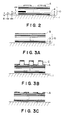
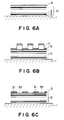
- Masque (Mo) du type à réflexion, utilisable dans un appareil d'exposition comportant un système optique de projection avec plusieurs miroirs (M1, M2, M3) placés entre le masque et une pièce d'oeuvre (W) destinés à transférer un motif du masque sur la pièce d'oeuvre à l'aide d'un rayonnement de rayons X mous ou d'ultraviolet lointain, caractérisé en ce que :
ledit masque (Mo) possède une surface réfléchissante (10 ; 10 ; 24) constituée par un film multicouche (2 à 5 ; 2 à 5 ; 2 à 5), et une partie non réfléchissante (A ; D ; 21 ; 22) prévue dans ou sur ladite surface réfléchissante pour définir le motif ; et dans lequel ladite partie non réfléchissante (A ; D ; 21 ; 22) sert à atténuer le rayonnement de rayons X mous ou d'ultraviolet lointain. - Masque selon la revendication 1, dans lequel ladite partie non réfléchissante (A ; D ; 21) comprend une matière absorbante disposée sur ledit film multicouche (2 à 5 ; 2 à 5 ; 24).
- Masque selon la revendication 1, dans lequel ladite partie non réfléchissante (22) est une partie (22) dudit film multicouche (2 à 5) dont l'ordre a été modifié.
- Masque du type à réflexion selon la revendication 1, dans lequel ladite matière absorbante de ladite partie non réfléchissante (A ; D ; 21 ; 22) a un coefficient de dilatation linéaire qui n'est pas plus grand que 5 x 10⁻⁵ deg-1 et une conductivité thermique qui n'est pas plus petite que 0,1 J/cm.s.deg.
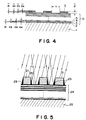
- Masque du type à réflexion selon la revendication 1, dans lequel ledit film multicouche (2 à 5) est formé de couches (2, 3, 4, 5) alternées de matières respectives différentes ayant des constantes optiques différentes.
- Masque du type à réflexion selon la revendication 5, dans lequel ledit film multicouche comporte des premières couches (2, 4, ...) ayant un indice de réfraction dont la partie nombre réel est plus petite et des secondes couches alternées (3, 5, ...) ayant un indice de réfraction dont la partie nombre réel est plus grande, lesquelles premières et secondes couches (2 à 5) sont respectivement plus loin et plus près de la surface de masque du type à réflexion.
- Procédé d'exposition destiné à transférer un motif d'un masque du type à réflexion sur une pièce d'oeuvre à l'aide d'un rayonnement de rayons X mous ou d'ultraviolet lointain, ledit procédé comprenant les étapes :de création d'un masque (Mo) du type à réflexion tel que revendiqué dans l'une quelconque des revendications 1 à 6 précédentes ; etde projection dudit rayonnement sur le masque (Mo), et d'exposition de la pièce d'oeuvre (W) au rayonnement réfléchi par le masque (Mo), à l'aide d'un système optique de projection comportant plusieurs miroirs (M1, M2, M3), en transférant ainsi le motif du masque (Mo) sur la pièce d'oeuvre (W).
- Procédé selon la revendication 7, dans lequel le motif du masque (Mo) projeté sur la pièce d'oeuvre (W) est à échelle réduite.
- Appareil d'exposition destiné à transférer un motif d'un masque du type à réflexion sur une pièce d'oeuvre à l'aide d'un rayonnement de rayons X mous ou d'ultraviolet lointain, ledit appareil comprenant :un moyen de maintien destiné à maintenir un masque (Mo) du type à réflexion ;un masque (Mo) du type à réflexion maintenu par ledit moyen de maintien, lequel masque (Mo) est tel que revendiqué dans l'une quelconque des revendications 1 à 6 précédentes ; etun moyen optique destiné à projeter ledit rayonnement sur le masque (Mo), et à exposer la pièce d'oeuvre (W) au rayonnement réfléchi par le masque (Mo), ledit moyen optique comprenant un système optique de projection comportant plusieurs miroirs (M1, M2, M3) destinés à projeter le motif du masque sur la pièce d'oeuvre, en transférant ainsi le motif du masque (Mo) sur la pièce d'oeuvre (W).
- Appareil selon la revendication 9, comprenant en outre un système optique destiné à projeter le motif du masque (Mo) sur la pièce d'oeuvre à une échelle réduite.
Applications Claiming Priority (12)
| Application Number | Priority Date | Filing Date | Title |
|---|---|---|---|
| JP33523/87 | 1987-02-18 | ||
| JP3352387A JPH0727198B2 (ja) | 1987-02-18 | 1987-02-18 | 多層膜反射型マスク |
| JP33522287A JP2545905B2 (ja) | 1987-12-29 | 1987-12-29 | 反射型マスクならびにこれを用いた露光方法 |
| JP335221/87 | 1987-12-29 | ||
| JP62335221A JPH01175735A (ja) | 1987-12-29 | 1987-12-29 | 反射型マスク及びその製造方法 |
| JP335220/87 | 1987-12-29 | ||
| JP33522387A JP2546312B2 (ja) | 1987-12-29 | 1987-12-29 | 反射型マスクおよび該反射型マスクを用いた露光装置と露光方法 |
| JP335223/87 | 1987-12-29 | ||
| JP62335220A JPH01175734A (ja) | 1987-12-29 | 1987-12-29 | 反射型マスク及びその製造方法 |
| JP335222/87 | 1987-12-29 | ||
| JP12136/87 | 1988-01-22 | ||
| JP1213688A JP2615741B2 (ja) | 1988-01-22 | 1988-01-22 | 反射型マスクならびにこれを用いた露光装置と露光方法 |
Publications (3)
| Publication Number | Publication Date |
|---|---|
| EP0279670A2 EP0279670A2 (fr) | 1988-08-24 |
| EP0279670A3 EP0279670A3 (fr) | 1990-03-14 |
| EP0279670B1 true EP0279670B1 (fr) | 1997-10-29 |
Family
ID=27548393
Family Applications (1)
| Application Number | Title | Priority Date | Filing Date |
|---|---|---|---|
| EP88301367A Expired - Lifetime EP0279670B1 (fr) | 1987-02-18 | 1988-02-18 | Masque par réflection |
Country Status (3)
| Country | Link |
|---|---|
| US (1) | US5052033A (fr) |
| EP (1) | EP0279670B1 (fr) |
| DE (1) | DE3856054T2 (fr) |
Families Citing this family (62)
| Publication number | Priority date | Publication date | Assignee | Title |
|---|---|---|---|---|
| JPH0797216B2 (ja) * | 1986-10-29 | 1995-10-18 | インタ−ナショナル・ビジネス・マシ−ンズ・コ−ポレ−ション | マスクの製造方法 |
| US4923772A (en) * | 1986-10-29 | 1990-05-08 | Kirch Steven J | High energy laser mask and method of making same |
| FR2653234A1 (fr) * | 1989-10-13 | 1991-04-19 | Philips Electronique Lab | Dispositif du type miroir dans le domaine des rayons x-uv. |
| US5182763A (en) * | 1989-12-28 | 1993-01-26 | Canon Kabushiki Kaisha | Reflection device |
| JPH03266842A (ja) * | 1990-03-16 | 1991-11-27 | Fujitsu Ltd | 反射型ホトリソグラフィ方法、反射型ホトリソグラフィ装置および反射型ホトマスク |
| JP2599513B2 (ja) * | 1990-06-25 | 1997-04-09 | インターナショナル・ビジネス・マシーンズ・コーポレイション | アブレーション・マスク |
| JP2979667B2 (ja) * | 1991-01-23 | 1999-11-15 | 株式会社ニコン | 反射型のx線露光用マスク |
| US5335256A (en) * | 1991-03-18 | 1994-08-02 | Canon Kabushiki Kaisha | Semiconductor substrate including a single or multi-layer film having different densities in the thickness direction |
| JP3025545B2 (ja) * | 1991-03-18 | 2000-03-27 | キヤノン株式会社 | X線リソグラフィ用マスクおよびx線リソグラフィ露光装置 |
| JP3047541B2 (ja) * | 1991-08-22 | 2000-05-29 | 株式会社日立製作所 | 反射型マスクおよび欠陥修正方法 |
| DE69220868T2 (de) * | 1991-09-07 | 1997-11-06 | Canon Kk | System zur Stabilisierung der Formen von optischen Elementen, Belichtungsvorrichtung unter Verwendung dieses Systems und Verfahren zur Herstellung von Halbleitervorrichtungen |
| US5485497A (en) * | 1991-11-12 | 1996-01-16 | Hitachi, Ltd. | Optical element and projection exposure apparatus employing the same |
| JP3012069B2 (ja) * | 1991-12-04 | 2000-02-21 | キヤノン株式会社 | X線露光用マスク構造体及びこれを用いたx線露光装置 |
| JPH07117605B2 (ja) * | 1992-03-13 | 1995-12-18 | 日本ピラー工業株式会社 | 回折格子 |
| JPH05281704A (ja) * | 1992-04-02 | 1993-10-29 | Nec Corp | 半導体集積回路用ホトマスク |
| US5304437A (en) * | 1992-04-03 | 1994-04-19 | At&T Bell Laboratories | Mask for x-ray pattern delineation |
| JPH0689848A (ja) * | 1992-07-20 | 1994-03-29 | Canon Inc | X線マスク構造体の作製方法及び該作製方法により作製されたx線マスク構造体、並びに該x線マスク構造体を用い作製されたデバイス |
| US5307395A (en) * | 1992-09-30 | 1994-04-26 | The United States Of America As Represented By The Secretary Of The Navy | Low-damage multilayer mirror for the soft X-ray region |
| JP3219502B2 (ja) * | 1992-12-01 | 2001-10-15 | キヤノン株式会社 | 反射型マスクとその製造方法、並びに露光装置と半導体デバイス製造方法 |
| US5356662A (en) * | 1993-01-05 | 1994-10-18 | At&T Bell Laboratories | Method for repairing an optical element which includes a multilayer coating |
| JPH0772318A (ja) * | 1993-04-28 | 1995-03-17 | Canon Inc | 反射装置とこれを用いた照明装置や露光装置、並びにデバイス製造方法 |
| JPH07240364A (ja) * | 1994-03-02 | 1995-09-12 | Canon Inc | 反射型マスク、その製造方法及び該マスクを用いた露光装置 |
| US5827622A (en) * | 1995-11-02 | 1998-10-27 | International Business Machines Corporation | Reflective lithographic mask |
| DE69702641T2 (de) * | 1996-03-07 | 2001-04-05 | Koninkl Philips Electronics Nv | Belichtungssystem und belichtungsgerät für uv-lithographie |
| JP3814359B2 (ja) * | 1996-03-12 | 2006-08-30 | キヤノン株式会社 | X線投影露光装置及びデバイス製造方法 |
| US6317479B1 (en) * | 1996-05-17 | 2001-11-13 | Canon Kabushiki Kaisha | X-ray mask, and exposure method and apparatus using the same |
| JP3774522B2 (ja) * | 1996-12-24 | 2006-05-17 | キヤノン株式会社 | 回折光学素子及びそれを有する光学機器 |
| US5978441A (en) * | 1997-12-01 | 1999-11-02 | Advanced Micro Devices, Inc. | Extreme ultraviolet lithography mask blank and manufacturing method therefor |
| WO2000003341A1 (fr) * | 1998-07-10 | 2000-01-20 | Ball Semiconductor, Inc. | Procede et systeme servant a generer un masque plat sur une surface tridimensionnelle |
| US6316150B1 (en) | 1998-08-24 | 2001-11-13 | Euv Llc | Low thermal distortion extreme-UV lithography reticle |
| JP3770542B2 (ja) | 1999-07-22 | 2006-04-26 | コーニング インコーポレイテッド | 遠紫外軟x線投影リソグラフィー法およびマスク装置 |
| US6596465B1 (en) | 1999-10-08 | 2003-07-22 | Motorola, Inc. | Method of manufacturing a semiconductor component |
| CA2361519C (fr) | 1999-11-29 | 2009-12-08 | Tohoku Techno Arch Co., Ltd | Element optique, comme un reflecteur de film multicouches et article semblable, procede de fabrication et appareil y faisant appel |
| DE10016008A1 (de) * | 2000-03-31 | 2001-10-11 | Zeiss Carl | Villagensystem und dessen Herstellung |
| US7261957B2 (en) * | 2000-03-31 | 2007-08-28 | Carl Zeiss Smt Ag | Multilayer system with protecting layer system and production method |
| US20070281109A1 (en) * | 2000-03-31 | 2007-12-06 | Carl Zeiss Smt Ag | Multilayer system with protecting layer system and production method |
| US6625251B2 (en) * | 2000-09-22 | 2003-09-23 | Ntt Advanced Technology Corporation | Laser plasma x-ray generation apparatus |
| US6821682B1 (en) * | 2000-09-26 | 2004-11-23 | The Euv Llc | Repair of localized defects in multilayer-coated reticle blanks for extreme ultraviolet lithography |
| US6776006B2 (en) | 2000-10-13 | 2004-08-17 | Corning Incorporated | Method to avoid striae in EUV lithography mirrors |
| JP2002245947A (ja) | 2000-12-15 | 2002-08-30 | Canon Inc | 細線を有する基板及びその製造方法及び電子源基板及び画像表示装置 |
| US6635391B2 (en) * | 2000-12-28 | 2003-10-21 | The Regents Of The University Of California | Method for fabricating reticles for EUV lithography without the use of a patterned absorber |
| JP2002299228A (ja) * | 2001-04-03 | 2002-10-11 | Nikon Corp | レチクル、それを用いた露光装置及び露光方法 |
| DE10123768C2 (de) * | 2001-05-16 | 2003-04-30 | Infineon Technologies Ag | Verfahren zur Herstellung einer lithographischen Reflexionsmaske insbesondere für die Strukturierung eines Halbleiterwafers sowie Reflexionsmaske |
| US7053988B2 (en) | 2001-05-22 | 2006-05-30 | Carl Zeiss Smt Ag. | Optically polarizing retardation arrangement, and microlithography projection exposure machine |
| US6967168B2 (en) * | 2001-06-29 | 2005-11-22 | The Euv Limited Liability Corporation | Method to repair localized amplitude defects in a EUV lithography mask blank |
| US6673520B2 (en) | 2001-08-24 | 2004-01-06 | Motorola, Inc. | Method of making an integrated circuit using a reflective mask |
| US6653053B2 (en) | 2001-08-27 | 2003-11-25 | Motorola, Inc. | Method of forming a pattern on a semiconductor wafer using an attenuated phase shifting reflective mask |
| DE10155112B4 (de) * | 2001-11-09 | 2006-02-02 | Infineon Technologies Ag | Reflexionsmaske für die EUV-Lithographie und Herstellungsverfahren dafür |
| US6986971B2 (en) * | 2002-11-08 | 2006-01-17 | Freescale Semiconductor, Inc. | Reflective mask useful for transferring a pattern using extreme ultraviolet (EUV) radiation and method of making the same |
| DE10259331B4 (de) * | 2002-12-18 | 2005-02-10 | Infineon Technologies Ag | Herstellungsverfahren für eine Photomaske für eine integrierte Schaltung und entsprechende Photomaske |
| DE10261137A1 (de) * | 2002-12-21 | 2004-07-15 | Carl Zeiss Smt Ag | Projektionsoptik für die Lithographie und Spiegel für eine solche |
| US6875546B2 (en) * | 2003-03-03 | 2005-04-05 | Freescale Semiconductor, Inc. | Method of patterning photoresist on a wafer using an attenuated phase shift mask |
| US7026076B2 (en) * | 2003-03-03 | 2006-04-11 | Freescale Semiconductor, Inc. | Method of patterning photoresist on a wafer using a reflective mask with a multi-layer ARC |
| US6986974B2 (en) * | 2003-10-16 | 2006-01-17 | Freescale Semiconductor, Inc. | Attenuated phase shift mask for extreme ultraviolet lithography and method therefore |
| JP2005302963A (ja) * | 2004-04-09 | 2005-10-27 | Canon Inc | 露光装置 |
| JP2006049837A (ja) * | 2004-06-30 | 2006-02-16 | Canon Inc | 厚膜部材パターンの製造方法 |
| US7485410B2 (en) * | 2004-06-30 | 2009-02-03 | Canon Kabushiki Kaisha | Method of manufacturing thick dielectric pattern and method of manufacturing image displaying apparatus |
| KR100607201B1 (ko) * | 2005-01-04 | 2006-08-01 | 삼성전자주식회사 | 극자외선 리소그래피 공정에서 웨이퍼 상의 임계 치수편차를 보정하는 방법 |
| JP5018787B2 (ja) * | 2006-12-27 | 2012-09-05 | 旭硝子株式会社 | Euvリソグラフィ用反射型マスクブランク |
| EP2028681B1 (fr) * | 2007-01-31 | 2014-04-23 | Asahi Glass Company, Limited | Ébauche de masque réfléchissant pour lithographie euv |
| NL2003305A (en) | 2008-08-21 | 2010-03-10 | Asml Holding Nv | Euv reticle substrates with high thermal conductivity. |
| US9195132B2 (en) * | 2014-01-30 | 2015-11-24 | Globalfoundries Inc. | Mask structures and methods of manufacturing |
Family Cites Families (6)
| Publication number | Priority date | Publication date | Assignee | Title |
|---|---|---|---|---|
| JPS57106031A (en) * | 1980-12-23 | 1982-07-01 | Toshiba Corp | Transferring device for fine pattern |
| US4693933A (en) * | 1983-06-06 | 1987-09-15 | Ovonic Synthetic Materials Company, Inc. | X-ray dispersive and reflective structures and method of making the structures |
| JPS60173551A (ja) * | 1984-02-20 | 1985-09-06 | Hideki Matsumura | X線など光線の反射投影によるパタ−ン転写法 |
| WO1987006028A2 (fr) * | 1986-03-28 | 1987-10-08 | Shimadzu Corporation | Masque reflechissant les rayons x et systeme de formation d'images utilisant ledit masque |
| EP0252734B1 (fr) * | 1986-07-11 | 2000-05-03 | Canon Kabushiki Kaisha | Système d'exposition, par projection en réduction, de rayons X, du type réflectif |
| US4923772A (en) * | 1986-10-29 | 1990-05-08 | Kirch Steven J | High energy laser mask and method of making same |
-
1988
- 1988-02-18 DE DE3856054T patent/DE3856054T2/de not_active Expired - Lifetime
- 1988-02-18 EP EP88301367A patent/EP0279670B1/fr not_active Expired - Lifetime
-
1990
- 1990-12-28 US US07/633,181 patent/US5052033A/en not_active Expired - Lifetime
Also Published As
| Publication number | Publication date |
|---|---|
| DE3856054T2 (de) | 1998-03-19 |
| EP0279670A3 (fr) | 1990-03-14 |
| EP0279670A2 (fr) | 1988-08-24 |
| US5052033A (en) | 1991-09-24 |
| DE3856054D1 (de) | 1997-12-04 |
Similar Documents
| Publication | Publication Date | Title |
|---|---|---|
| EP0279670B1 (fr) | Masque par réflection | |
| US11754917B2 (en) | Extreme ultraviolet mask blank with multilayer absorber and method of manufacture | |
| EP0708367B1 (fr) | Appareil pour décrire des motifs pour utilisation dans le domaine ultra-violet extrême | |
| JP3078163B2 (ja) | リソグラフィ用反射型マスクおよび縮小投影露光装置 | |
| US6833223B2 (en) | Multilayer-film reflective mirrors and optical systems comprising same | |
| KR100589240B1 (ko) | Euv 광학 요소의 캡핑 층 | |
| US6048652A (en) | Backside polish EUV mask and method of manufacture | |
| JP3219502B2 (ja) | 反射型マスクとその製造方法、並びに露光装置と半導体デバイス製造方法 | |
| CN110501769A (zh) | 用于光刻设备内的膜和包括这种膜的光刻设备 | |
| JPH11506876A (ja) | 紫外線リトグラフィー用の結像システム及び装置 | |
| CN1312531C (zh) | 光刻掩模制造 | |
| JP2545905B2 (ja) | 反射型マスクならびにこれを用いた露光方法 | |
| JPH0727198B2 (ja) | 多層膜反射型マスク | |
| JPH0868897A (ja) | 反射鏡およびその製造方法 | |
| US6830851B2 (en) | Photolithographic mask fabrication | |
| JP2006194764A (ja) | 多層膜反射鏡および露光装置 | |
| JPH10339799A (ja) | 反射鏡及びその製造方法 | |
| JP2615741B2 (ja) | 反射型マスクならびにこれを用いた露光装置と露光方法 | |
| JPH05144710A (ja) | 光学素子及びその製造方法 | |
| US8906582B2 (en) | Blank masks for extreme ultra violet lithography, methods of fabricating the same, and methods of correcting registration errors thereof | |
| JP7295260B2 (ja) | 多層吸収体を備えた極紫外線マスクブランクおよび製造方法 | |
| US11815803B2 (en) | Multilayer extreme ultraviolet reflector materials | |
| JP2675263B2 (ja) | 反射型マスクを用いた露光装置および露光方法 | |
| JPH01175734A (ja) | 反射型マスク及びその製造方法 | |
| JP2615741C (fr) |
Legal Events
| Date | Code | Title | Description |
|---|---|---|---|
| PUAI | Public reference made under article 153(3) epc to a published international application that has entered the european phase |
Free format text: ORIGINAL CODE: 0009012 |
|
| AK | Designated contracting states |
Kind code of ref document: A2 Designated state(s): DE FR GB |
|
| PUAL | Search report despatched |
Free format text: ORIGINAL CODE: 0009013 |
|
| AK | Designated contracting states |
Kind code of ref document: A3 Designated state(s): DE FR GB |
|
| 17P | Request for examination filed |
Effective date: 19900730 |
|
| 17Q | First examination report despatched |
Effective date: 19930322 |
|
| GRAG | Despatch of communication of intention to grant |
Free format text: ORIGINAL CODE: EPIDOS AGRA |
|
| GRAH | Despatch of communication of intention to grant a patent |
Free format text: ORIGINAL CODE: EPIDOS IGRA |
|
| GRAH | Despatch of communication of intention to grant a patent |
Free format text: ORIGINAL CODE: EPIDOS IGRA |
|
| GRAA | (expected) grant |
Free format text: ORIGINAL CODE: 0009210 |
|
| AK | Designated contracting states |
Kind code of ref document: B1 Designated state(s): DE FR GB |
|
| REF | Corresponds to: |
Ref document number: 3856054 Country of ref document: DE Date of ref document: 19971204 |
|
| ET | Fr: translation filed | ||
| PLBE | No opposition filed within time limit |
Free format text: ORIGINAL CODE: 0009261 |
|
| STAA | Information on the status of an ep patent application or granted ep patent |
Free format text: STATUS: NO OPPOSITION FILED WITHIN TIME LIMIT |
|
| 26N | No opposition filed | ||
| REG | Reference to a national code |
Ref country code: GB Ref legal event code: IF02 |
|
| PGFP | Annual fee paid to national office [announced via postgrant information from national office to epo] |
Ref country code: GB Payment date: 20070214 Year of fee payment: 20 |
|
| PGFP | Annual fee paid to national office [announced via postgrant information from national office to epo] |
Ref country code: DE Payment date: 20070418 Year of fee payment: 20 |
|
| REG | Reference to a national code |
Ref country code: GB Ref legal event code: PE20 |
|
| PGFP | Annual fee paid to national office [announced via postgrant information from national office to epo] |
Ref country code: FR Payment date: 20070221 Year of fee payment: 20 |
|
| PG25 | Lapsed in a contracting state [announced via postgrant information from national office to epo] |
Ref country code: GB Free format text: LAPSE BECAUSE OF EXPIRATION OF PROTECTION Effective date: 20080217 |