EP0197560A2 - Verfahren und Anordnung zur Aufzeichnung von PCM-Signalen - Google Patents
Verfahren und Anordnung zur Aufzeichnung von PCM-Signalen Download PDFInfo
- Publication number
- EP0197560A2 EP0197560A2 EP86104920A EP86104920A EP0197560A2 EP 0197560 A2 EP0197560 A2 EP 0197560A2 EP 86104920 A EP86104920 A EP 86104920A EP 86104920 A EP86104920 A EP 86104920A EP 0197560 A2 EP0197560 A2 EP 0197560A2
- Authority
- EP
- European Patent Office
- Prior art keywords
- data
- channels
- pcm signal
- bits
- recording
- Prior art date
- Legal status (The legal status is an assumption and is not a legal conclusion. Google has not performed a legal analysis and makes no representation as to the accuracy of the status listed.)
- Granted
Links
Images


Classifications
-
- G—PHYSICS
- G11—INFORMATION STORAGE
- G11B—INFORMATION STORAGE BASED ON RELATIVE MOVEMENT BETWEEN RECORD CARRIER AND TRANSDUCER
- G11B20/00—Signal processing not specific to the method of recording or reproducing; Circuits therefor
- G11B20/02—Analogue recording or reproducing
- G11B20/08—Pulse-modulation recording or reproducing
-
- G—PHYSICS
- G11—INFORMATION STORAGE
- G11B—INFORMATION STORAGE BASED ON RELATIVE MOVEMENT BETWEEN RECORD CARRIER AND TRANSDUCER
- G11B20/00—Signal processing not specific to the method of recording or reproducing; Circuits therefor
- G11B20/10—Digital recording or reproducing
- G11B20/10527—Audio or video recording; Data buffering arrangements
-
- G—PHYSICS
- G11—INFORMATION STORAGE
- G11B—INFORMATION STORAGE BASED ON RELATIVE MOVEMENT BETWEEN RECORD CARRIER AND TRANSDUCER
- G11B20/00—Signal processing not specific to the method of recording or reproducing; Circuits therefor
- G11B20/10—Digital recording or reproducing
- G11B20/18—Error detection or correction; Testing, e.g. of drop-outs
- G11B20/1806—Pulse code modulation systems for audio signals
- G11B20/1809—Pulse code modulation systems for audio signals by interleaving
Definitions
- the present invention relates to a recording and/or reproducing technique for PCM signals, and in particular to PCM signal recording and/or reproducing method and apparatus suitable for recording and/or reproducing audio PCM signals onto and/or from a digital audio tape recorder (hereafter referred to as DAT).
- DAT digital audio tape recorder
- the DAT for converting the audio signal into PCM signals and recording the PCM signals onto the magnetic tape is excellent in tone quality and free from quality deterioration caused by the recording and reproducing operation.
- R-DAT rotary-head type digital audio tape recorder
- the first PCM signal having a sampling frequency of 48 KHz, a quantization of 16 bits per sample, and the number of channels 2 (left and right) was recorded onto the tape as an experimental format of the R-DAT.
- the first PCM signal corresponds to the B-mode specification in the PCM signal transmission of the satellite broadcast in Japan.
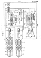
- Fig. 1 shows configuration of an embodiment of the present invention. In Fig. 1, however, it is possible to record the above described PCM signal onto tape by removing blocks 1 to 4 and blocks 8 to 11 of the C channel and D channel, removing blocks 7 and 13, and connecting the input of the block 7 and the output of the block 13 to an external circuit.
- Fig. 2 shows a record pattern on the magnetic tape of the R-DAT described on page 41 of the aforementioned literature.
- blocks of the above described first PCM signal are recorded alternately on a plus azimuth track 34 and on a minus azimuth track 35 128 by 128.
- Head gaps of heads 32a and 32b shown in Fig. 1 are slanted with respect to a face perpendicular to the record direction as indicated by oblique lines of Fig. 2.
- the first PCM signal is also recorded in the directions indicated by oblique lines of Fig. 2. These tracks are referred to as azimuth tracks.
- the terms "plus azimuth” and "minus aximuth” mean that the oblique directions of tracks 34 and 35 are opposite each other as illustrated by oblique lines.
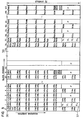
- Figs. 3 and 4 show configuration of an example of PCM data recorded on respective tracks of Fig. 2.
- Fig. 3 shows data arrangement on the plus azimuth track 34 of Fig. 2.
- Fig. 4 shows data arrangement on the minus aximuth track 35 of Fig. 2.
- Numeral 36 denotes one symbol unit which consists of 8 bits.
- one-word signal comprises two symbols, an upper symbol and a lower symbol.
- One block comprises 32 symbols and 128 blocks are recorded on one track.
- Numeral 38 denotes a first error detection and correction code Q and numeral 37 denotes a second error detection and correction code P.
- Letter L represents left channel data and letter R represents right channel data.
- the suffix following L or R represents a serial number of the left channel data or right channel data.
- the suffix 0, 2, 4, ... represents even-numbered data and the suffix l, 3, 5, ... represents odd-numbered data.
- Letter U represents the above described upper symbol and letter 1 represents the above described lower symbol.
- Data dispersion is conducted in data recording so that error compensation may be effected by means of means value interpolation even-if a large burst error occurs in data reproduction. That is to say, even-numbered data of the left channel are recorded on former halves of plus azimuth tracks and odd-numbered data of the left channel are recorded on latter halves of minus azimuth tracks. And even-numbered data of the right channel are recorded on former halves of minus azimuth tracks and odd-numbered data of the right channel are recorded on letter halves of plus azimuth tracks. Examples of this arrangement will now be described by referring to Figs. 3 and 4. Even-numbered data Lou of the left channel is indicated on block No. 0 of Fig. 3.
- An object of the present invention is to provide a method and an apparatus for recording and/or reproducing PCM signals capable of recording the second PCM signal source which is different in sampling frequency, the number of quantized bits per sample, and the number of channels.
- words of a P C M signal which is different in sampling frequency, the number of quantized bits per sample, and the number of channels are interchanged in a predetermined sequence while taking a fixed number of words as unit in order to be recorded in a data arrangement optimum with respect to burst errors.
- Fig. 1 shows configuration of an R-DAT.
- analog signals of four channels A, B, C and D are supplied from an input terminal 1.
- the input signal is amplified to a predetermined level by an amplifier circuit 2, limited in bandwidth by a filter 3, and sampled by a sample and hold circuit 4.
- Input signals thus sampled are successively supplied to an A/D converter 6 through a switch circuit 5 to be converted into PCM signals.
- the PCM signals supplied from the A/D converter 6 undergo interchange according to a predetermined sequence in a data conversion circuit 7 and are written into a RAM 15 through a bus line 14.
- the PCM signals are exchanged between the RAM 15 and the error correction circuit 20, and error correction codes ; for detecting and correcting errors in the reproduction operation are added to the PCM signals.
- the address of the RAM 15 is controlled by address generation circuits 17 to 19 and an address switch circuit 16 to arrange PCM signals according to the above described format illustrated in Figs. 3 and 4.
- data are read out of the ROM 15 block by block and are modulated by a modulation circuit 23.
- Control signals such as synchronization signals are added to the modulated data by a control signal generation circuit 24 and a switch circuit 25.
- the resultant data are amplified to a predetermined level by a record amplifier 26 and supplied to a rotary head 32 through a switch circuit 31 to be recorded on the magnetic tape 33.
- the switch circuit 31 is changed over between the record operation and reproduction operation.
- a timing generation circuit 21 generates timing signals for controlling the entire circuit (blocks 4 to 13, 15 to 20, and 23 to 28), on the basis of clocks generated by an oscillation circuit 22.
- the switch circuit 31 In reproduction operation, the switch circuit 31 is changed over to the reproduction position. Signals reproduced by the rotary head 32 are supplied to a reproduction amplifier 30 to undergo amplification and waveform equalization. After the resultant signals are converted into digtal signals by a data strobe circuit 29, data demodulation and synchronization signal detection are effected by a demodulation circuit 27 and a synchronization detection circuit 28, respectively. The synchronization signal thus detected is used as a reference for data reproduction.
- the data demodulated by the demodulation circuit 27 are stored into the RAM 15 through the bus line 14 and thereafter undergo the data rearrangement by the address generation circuits 17 to 19 and the address switch circuit 16 and the error correction by the error correction circuit 20. The resultant data are supplied to a data conversion circuit 13 through the bus line 14.
- the data undergo data interchange which is reverse to that effected in the data conversion circuit 7.
- the PCM signals rearranged in time series sequence are successively converted into analog signals by a D/A converter 12 and resampled for respective channels by a sample and hold circuit 11.
- the resampled analog signal of each channel is sent out from an output terminal 8 through a filter 10 and an amplifier circuit 9.
- a part 39 of Fig. 1 surrounded by a broken line is so configured as to be suitable for recording the above described first PCM signal having a sampling frequency of 48 KHz, a quantization of 16 bits per sample, and two channels.
- the above described second PCM signal having a sampling frequency of 32 KHz, a quantization of 12 bits per sample, and 4 channels by adding blocks 1 to 4 and 8 to 11 of the channels C and D as well as the data conversion circuits 7 and 13.
- Fig. 5 shows the output data sequence of the A/D converter 6 when the above described first PCM signal source having two channels (left and right) is recorded.
- the subscript represents the order of each data on time series and is supplied to each word composed of 16 bits.
- This output data is then transmitted to the RAM 15.
- the PCM signals thus supplied are rearranged so that even-numbered data and odd-numbered data of each channel may be disposed on different tracks and also separated in the track direction as described before with reference to Figs. 3, 4 and 2.
- the sequence of the output data of the A/D converter 6 becomes as shown in Fig. 6(a). It is also possible to record the second PCM signal without effecting interchange because the second PCM signal has as many data bits per hour as the above described first PCM signal having a sampling frequency of 48 KHz, a quantization of 16 bits per sample, and two channels. In this case, however, even-numbered data positions and odd-numbered data positions of each channel does not correspond to even-numbered positions and odd-numbered positions of the left channel data and the right channel data as illustrated in Fig. 5.
- Figs. 6(b) and 6(c) data interchange as illustrated in Figs. 6(b) and 6(c) is conducted in the data conversion circuit 7. That is to say, each word composed of 12 bits (A o , for example) as illustrated in Fig. 6(a) is divided into 4-bit groups (A , A ob , A oc ) as illustrated in Fig. 6(b). As illustrated in Fig. 6(c), data interchange is effected with 16 words (A oa , A ob , A oc , C oa ) taken as unit as follows.
- Fig. 6(d) corresponds to Fig. 5.
- data of channels A and C are disposed in positions of the left channel, and data of channels B and D are disposed in positions of the right channel.
- data of channels A and B are disposed in positions of the channel L and dispose data of channels C and D in positions of the channel R.
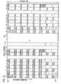
- Figs. 7 and 8 show data configuration when the second PCM signal having a sampling frequency of 32 KHz, a quantization of 12 bits per sample, and four channels is recorded on the tape by using the conversion illustrated in Fig. 6.
- Fig. 7 shows the configuration of data recorded on the azimuth track 34 illustrated in Fig. 2.
- Fig. 8 shows the configuration of data recorded on the minus azimuth track 35 illustrated in Fig. 2.
- Figs. 7 and 8 are represented by marks of Fig. 6(e). In the same way as Figs. 3 and 4, even-numbered data and odd-numbered data of each channel are disposed on adjacent tracks and at a distance on the track direction.
- Fig. 9 shows an example of configuration of the data conversion circuits 7 and 13.
- the circuit of Fig. 9 is composed of a RAM 45, an address switch circuit 46, an adder circuit 47, counters 49 and 50, and an offset generation circuit.
- Fig. 10 is a timing chart of input and output signals of the circuit illustrated in Fig. 9.
- Data 40-1 supplied from an input terminal 40 are written into the RAM 45.
- the data read out of the RAM 45 are sent out from an output terminal 41 as data 41-1.
- Data conversion is effected by controlling the read address and write address of the RAM 45.
- the capacity cf the RAM is 4 bits x 21 words.
- a counter 49 is a 21-step counter which successively counts clock signals 43-1 supplied from an input terminal 43. The value contained in the counter 49 is used as the write address and the read address of the RAM 45.
- a counter 50 is a 48-step counter and represents the serial number of the supplied data. The counter 50 is reset at the beginning of conversion by a reset signal 44-1 supplied from an input terminal 44.
- the read address is controlled by adding in the adder circuit 47 the value of the counter 49 to an offset value sent out from the offset generation circuit 48 on the basis of the value of the counter 50.
- Numeral 42 denotes an input terminal for a data write control signal 42-1 of the RAM 45.
- the address switch circuit 46 assumes the position connected to the counter 49. At the same time, the RAM write control signal 42-1 is supplied to the RAM 45 to write data therein. When the clock signal 43-1 is "0", the address switch circuit 46 is changed over to a position connected to the adder circuit 47 to read out data.
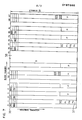
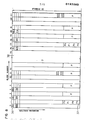
- Table 1 shows an example of input and output data and address state of the RAM 45 during data conversion in the data conversion circuit of Fig. 9.
- Data conversion effected in the data conversion circuit 7 during the recording operation is shown in Table 1.
- Data conversion during the reproduction can be similarly effected in the data conversion circuit 13.
- the write address is the value of the counter 49.
- the read address is obtained by adding the offset value to the write address.
- the addition of the offset value to the write address in the adder circuit 47 is addition, modulo 21.
- the present invention heretofore described, it is possible to record the second PCM signal having a sampling frequency of 32 KHz, a quantization of 12 bits per sample, and 4 channels in data configuration optimum to burst errors.
- the rotary-head type DAT is used. It is also possible to cope with a fixed-head type DAT by using similar conversion. Even it input and output signals are digital signals, they can be handled with no problem by configuring the input and output signal as shown in Fig. 6(a).
Landscapes
- Engineering & Computer Science (AREA)
- Signal Processing (AREA)
- Multimedia (AREA)
- Signal Processing For Digital Recording And Reproducing (AREA)
Applications Claiming Priority (2)
| Application Number | Priority Date | Filing Date | Title |
|---|---|---|---|
| JP74234/85 | 1985-04-10 | ||
| JP60074234A JP2574744B2 (ja) | 1985-04-10 | 1985-04-10 | Pcm信号記録再生装置 |
Publications (3)
| Publication Number | Publication Date |
|---|---|
| EP0197560A2 true EP0197560A2 (de) | 1986-10-15 |
| EP0197560A3 EP0197560A3 (en) | 1987-08-19 |
| EP0197560B1 EP0197560B1 (de) | 1990-07-04 |
Family
ID=13541269
Family Applications (1)
| Application Number | Title | Priority Date | Filing Date |
|---|---|---|---|
| EP86104920A Expired - Lifetime EP0197560B1 (de) | 1985-04-10 | 1986-04-10 | Verfahren und Anordnung zur Aufzeichnung von PCM-Signalen |
Country Status (6)
| Country | Link |
|---|---|
| US (1) | US4758907A (de) |
| EP (1) | EP0197560B1 (de) |
| JP (1) | JP2574744B2 (de) |
| KR (1) | KR900005060B1 (de) |
| CN (1) | CN86102443B (de) |
| DE (1) | DE3672368D1 (de) |
Cited By (3)
| Publication number | Priority date | Publication date | Assignee | Title |
|---|---|---|---|---|
| EP0278702A3 (en) * | 1987-02-06 | 1990-04-04 | Sony Corporation | Apparatus for reproducing a digital signal |
| EP0411998A3 (en) * | 1989-07-29 | 1993-04-07 | Sony Corporation | 4-channel pcm signal processing apparatus |
| US5285326A (en) * | 1989-07-29 | 1994-02-08 | Sony Corporation | Digital signal processor for converting between 4-channel PCM signals and 2-channel PCM signals |
Families Citing this family (22)
| Publication number | Priority date | Publication date | Assignee | Title |
|---|---|---|---|---|
| JP2557624B2 (ja) * | 1986-03-17 | 1996-11-27 | 株式会社 日立メディコ | デイジタルデ−タ記録再生装置 |
| US4903025A (en) * | 1987-04-07 | 1990-02-20 | Nakamichi Corporation | Signal path setting circuit |
| JPH069108B2 (ja) * | 1988-02-05 | 1994-02-02 | ソニーマグネスケール株式会社 | 多チャンネルpcmデータ記録方法 |
| JP2694343B2 (ja) * | 1988-04-18 | 1997-12-24 | 株式会社日立製作所 | Pcm音声受信機 |
| JP2585710B2 (ja) * | 1988-05-13 | 1997-02-26 | 株式会社日立製作所 | Pcm信号記録再生装置及びpcm信号記録再生方法 |
| JP2638091B2 (ja) * | 1988-06-24 | 1997-08-06 | ソニー株式会社 | データ伝送方法 |
| US4972190A (en) * | 1989-06-12 | 1990-11-20 | Aerocorp Technologies Inc. | Analog signal digitizer for recording on a video |
| US5680378A (en) * | 1990-09-27 | 1997-10-21 | Casio Computer Co., Ltd. | Digital recorder for recording/reproducing events formed by dividing audio data in a designated order |
| JPH04232666A (ja) * | 1990-12-28 | 1992-08-20 | Casio Comput Co Ltd | デジタルレコーダ |
| JP2969187B2 (ja) * | 1990-12-28 | 1999-11-02 | カシオ計算機株式会社 | デジタルレコーダ |
| JP2979100B2 (ja) * | 1991-03-13 | 1999-11-15 | カシオ計算機株式会社 | デジタルレコーダ |
| US5245667A (en) * | 1991-04-03 | 1993-09-14 | Frox, Inc. | Method and structure for synchronizing multiple, independently generated digital audio signals |
| JP3311770B2 (ja) * | 1992-02-03 | 2002-08-05 | ローム株式会社 | ハードディスクドライブ装置 |
| EP0593173B1 (de) * | 1992-10-16 | 1998-11-11 | Matsushita Electric Industrial Co., Ltd. | Gerät zur Aufzeichnung von Datensignalen mittels Steuerung der Frequenzcharakteristiken der Datensignale |
| US5940238A (en) * | 1996-06-07 | 1999-08-17 | Seagate Technology, Inc. | Mechanism to reduce adjacent track interference in a magnetic tape data storage system |
| US6496328B1 (en) | 1999-12-30 | 2002-12-17 | Advanced Research Corporation | Low inductance, ferrite sub-gap substrate structure for surface film magnetic recording heads |
| US6947247B2 (en) * | 2003-03-05 | 2005-09-20 | Advanced Research Corporation | Large angle azimuth recording and head configurations |
| US8144424B2 (en) | 2003-12-19 | 2012-03-27 | Dugas Matthew P | Timing-based servo verify head and magnetic media made therewith |
| WO2005109405A1 (en) | 2004-05-04 | 2005-11-17 | Advanced Research Corporation | Intergrated thin film subgap/subpole structure for arbitrary gap pattern, magnetic recording heads and method of making the same |
| WO2009121073A1 (en) | 2008-03-28 | 2009-10-01 | Advanced Research Corporation | Thin film planar arbitrary gap pattern magnetic head |
| WO2011014836A2 (en) | 2009-07-31 | 2011-02-03 | Advanced Research Corporation | Erase drive systems and methods of erasure for tape data cartridge |
| CN103178867A (zh) * | 2013-04-03 | 2013-06-26 | 上海航天测控通信研究所 | 一种WiFi头戴设备 |
Family Cites Families (8)
| Publication number | Priority date | Publication date | Assignee | Title |
|---|---|---|---|---|
| JPS58188314A (ja) * | 1982-04-26 | 1983-11-02 | Sony Corp | Pcmデータの記録装置及び再生装置 |
| EP0112868A1 (de) * | 1982-07-06 | 1984-07-11 | Beckman Instruments, Inc. | Probenbehälter mit mehreren räumen für das ultrazentrifugieren |
| JPH0634305B2 (ja) * | 1983-03-04 | 1994-05-02 | ソニー株式会社 | デイジタルデイスクによるデ−タ伝送システム |
| JPH0661156B2 (ja) * | 1983-05-21 | 1994-08-10 | ソニー株式会社 | エラ−訂正のための符号化方法 |
| KR900001222B1 (ko) * | 1983-06-15 | 1990-03-05 | 가부시기가이샤 히다찌세이사꾸쇼 | Pcm 신호의 기록 재생장치 |
| JPS601940A (ja) * | 1983-06-17 | 1985-01-08 | Sony Corp | データ列伝送システム |
| JPH07118160B2 (ja) * | 1983-06-18 | 1995-12-18 | ソニー株式会社 | ディジタル情報信号の記録方法 |
| JPH07122966B2 (ja) * | 1984-03-19 | 1995-12-25 | 株式会社日立製作所 | 回転ヘッド型pcmレコーダの記録方法及び再生方法 |
-
1985
- 1985-04-10 JP JP60074234A patent/JP2574744B2/ja not_active Expired - Lifetime
-
1986
- 1986-04-03 KR KR1019860002542A patent/KR900005060B1/ko not_active Expired
- 1986-04-09 CN CN86102443A patent/CN86102443B/zh not_active Expired
- 1986-04-10 US US06/850,110 patent/US4758907A/en not_active Expired - Lifetime
- 1986-04-10 EP EP86104920A patent/EP0197560B1/de not_active Expired - Lifetime
- 1986-04-10 DE DE8686104920T patent/DE3672368D1/de not_active Expired - Lifetime
Cited By (3)
| Publication number | Priority date | Publication date | Assignee | Title |
|---|---|---|---|---|
| EP0278702A3 (en) * | 1987-02-06 | 1990-04-04 | Sony Corporation | Apparatus for reproducing a digital signal |
| EP0411998A3 (en) * | 1989-07-29 | 1993-04-07 | Sony Corporation | 4-channel pcm signal processing apparatus |
| US5285326A (en) * | 1989-07-29 | 1994-02-08 | Sony Corporation | Digital signal processor for converting between 4-channel PCM signals and 2-channel PCM signals |
Also Published As
| Publication number | Publication date |
|---|---|
| KR860008548A (ko) | 1986-11-17 |
| KR900005060B1 (ko) | 1990-07-19 |
| JP2574744B2 (ja) | 1997-01-22 |
| US4758907A (en) | 1988-07-19 |
| EP0197560A3 (en) | 1987-08-19 |
| JPS61236074A (ja) | 1986-10-21 |
| CN86102443B (zh) | 1988-08-03 |
| CN86102443A (zh) | 1986-11-05 |
| EP0197560B1 (de) | 1990-07-04 |
| DE3672368D1 (de) | 1990-08-09 |
Similar Documents
| Publication | Publication Date | Title |
|---|---|---|
| EP0197560B1 (de) | Verfahren und Anordnung zur Aufzeichnung von PCM-Signalen | |
| US4866636A (en) | Method and apparatus for uniformly encoding data occurring with different word lengths | |
| US4675754A (en) | Magnetic recorder/reproducer | |
| EP0178589B1 (de) | Verfahren und Anordnung zur Aufzeichnung von PCM-Signalen | |
| EP0130091B1 (de) | Gerät zur Aufzeichnung und/oder Wiedergabe von digitalen Informationssignalen | |
| EP0209141B1 (de) | PCM-Signal-Aufzeichnungs- und Wiedergabeeinrichtung | |
| US4961204A (en) | PCM signal generating/reproducing apparatus | |
| US5247396A (en) | PCM signal recording method and apparatus for recording four-channel data to be compatible with two-channel data | |
| US5559644A (en) | Data recording/reproducing apparatus having a first error correcting code on both sides of a main data area of each azimuth track | |
| JPS5965906A (ja) | マルチチヤンネル記録再生装置 | |
| JPS60209973A (ja) | 回転ヘッド形磁気記録再生装置およびその記録再生方式 | |
| JP2546189B2 (ja) | 回転ヘッド形磁気再生装置及びこれに用いる信号処理回路 | |
| JPH0191376A (ja) | 補助情報記録方法 | |
| JPH05250814A (ja) | ディジタル磁気記録再生装置 | |
| JPS61230678A (ja) | Pcm信号記録再生装置 | |
| JPS6136305B2 (de) | ||
| JPH0782713B2 (ja) | Pcm信号記録再生装置及び再生装置 | |
| JPH0519785B2 (de) | ||
| JPH0514354B2 (de) | ||
| JPS6055557A (ja) | ディジタル音響記録再生装置 | |
| JPH0782712B2 (ja) | ディジタル信号記録再生装置 | |
| JPS61214281A (ja) | Pcm信号記録再生装置 | |
| JPH027265A (ja) | 磁気記録再生装置 | |
| JPH01303674A (ja) | デジタル信号用記録再生方式 | |
| JPS63187741A (ja) | デイジタル信号の伝送方式 |
Legal Events
| Date | Code | Title | Description |
|---|---|---|---|
| PUAI | Public reference made under article 153(3) epc to a published international application that has entered the european phase |
Free format text: ORIGINAL CODE: 0009012 |
|
| 17P | Request for examination filed |
Effective date: 19860410 |
|
| AK | Designated contracting states |
Kind code of ref document: A2 Designated state(s): DE FR GB |
|
| PUAL | Search report despatched |
Free format text: ORIGINAL CODE: 0009013 |
|
| AK | Designated contracting states |
Kind code of ref document: A3 Designated state(s): DE FR GB |
|
| 17Q | First examination report despatched |
Effective date: 19880226 |
|
| GRAA | (expected) grant |
Free format text: ORIGINAL CODE: 0009210 |
|
| AK | Designated contracting states |
Kind code of ref document: B1 Designated state(s): DE FR GB |
|
| REF | Corresponds to: |
Ref document number: 3672368 Country of ref document: DE Date of ref document: 19900809 |
|
| ET | Fr: translation filed | ||
| PLBE | No opposition filed within time limit |
Free format text: ORIGINAL CODE: 0009261 |
|
| 26N | No opposition filed | ||
| REG | Reference to a national code |
Ref country code: GB Ref legal event code: IF02 |
|
| PGFP | Annual fee paid to national office [announced via postgrant information from national office to epo] |
Ref country code: FR Payment date: 20050322 Year of fee payment: 20 |
|
| PGFP | Annual fee paid to national office [announced via postgrant information from national office to epo] |
Ref country code: GB Payment date: 20050324 Year of fee payment: 20 |
|
| REG | Reference to a national code |
Ref country code: GB Ref legal event code: PE20 |
|
| PGFP | Annual fee paid to national office [announced via postgrant information from national office to epo] |
Ref country code: DE Payment date: 20050609 Year of fee payment: 20 |
|
| PG25 | Lapsed in a contracting state [announced via postgrant information from national office to epo] |
Ref country code: GB Free format text: LAPSE BECAUSE OF EXPIRATION OF PROTECTION Effective date: 20060409 |