EP0140814B1 - Système de contrôle à conservation d'énergie - Google Patents
Système de contrôle à conservation d'énergie Download PDFInfo
- Publication number
- EP0140814B1 EP0140814B1 EP84630152A EP84630152A EP0140814B1 EP 0140814 B1 EP0140814 B1 EP 0140814B1 EP 84630152 A EP84630152 A EP 84630152A EP 84630152 A EP84630152 A EP 84630152A EP 0140814 B1 EP0140814 B1 EP 0140814B1
- Authority
- EP
- European Patent Office
- Prior art keywords
- power
- signal
- processor
- control system
- control
- Prior art date
- Legal status (The legal status is an assumption and is not a legal conclusion. Google has not performed a legal analysis and makes no representation as to the accuracy of the status listed.)
- Expired - Lifetime
Links
Images


Classifications
-
- G—PHYSICS
- G06—COMPUTING; CALCULATING OR COUNTING
- G06F—ELECTRIC DIGITAL DATA PROCESSING
- G06F1/00—Details not covered by groups G06F3/00 - G06F13/00 and G06F21/00
- G06F1/26—Power supply means, e.g. regulation thereof
- G06F1/32—Means for saving power
- G06F1/3203—Power management, i.e. event-based initiation of a power-saving mode
- G06F1/3206—Monitoring of events, devices or parameters that trigger a change in power modality
- G06F1/3215—Monitoring of peripheral devices
-
- G—PHYSICS
- G06—COMPUTING; CALCULATING OR COUNTING
- G06F—ELECTRIC DIGITAL DATA PROCESSING
- G06F1/00—Details not covered by groups G06F3/00 - G06F13/00 and G06F21/00
- G06F1/26—Power supply means, e.g. regulation thereof
- G06F1/32—Means for saving power
- G06F1/3203—Power management, i.e. event-based initiation of a power-saving mode
- G06F1/3234—Power saving characterised by the action undertaken
- G06F1/3287—Power saving characterised by the action undertaken by switching off individual functional units in the computer system
-
- Y—GENERAL TAGGING OF NEW TECHNOLOGICAL DEVELOPMENTS; GENERAL TAGGING OF CROSS-SECTIONAL TECHNOLOGIES SPANNING OVER SEVERAL SECTIONS OF THE IPC; TECHNICAL SUBJECTS COVERED BY FORMER USPC CROSS-REFERENCE ART COLLECTIONS [XRACs] AND DIGESTS
- Y02—TECHNOLOGIES OR APPLICATIONS FOR MITIGATION OR ADAPTATION AGAINST CLIMATE CHANGE
- Y02D—CLIMATE CHANGE MITIGATION TECHNOLOGIES IN INFORMATION AND COMMUNICATION TECHNOLOGIES [ICT], I.E. INFORMATION AND COMMUNICATION TECHNOLOGIES AIMING AT THE REDUCTION OF THEIR OWN ENERGY USE
- Y02D10/00—Energy efficient computing, e.g. low power processors, power management or thermal management
-
- Y—GENERAL TAGGING OF NEW TECHNOLOGICAL DEVELOPMENTS; GENERAL TAGGING OF CROSS-SECTIONAL TECHNOLOGIES SPANNING OVER SEVERAL SECTIONS OF THE IPC; TECHNICAL SUBJECTS COVERED BY FORMER USPC CROSS-REFERENCE ART COLLECTIONS [XRACs] AND DIGESTS
- Y02—TECHNOLOGIES OR APPLICATIONS FOR MITIGATION OR ADAPTATION AGAINST CLIMATE CHANGE
- Y02D—CLIMATE CHANGE MITIGATION TECHNOLOGIES IN INFORMATION AND COMMUNICATION TECHNOLOGIES [ICT], I.E. INFORMATION AND COMMUNICATION TECHNOLOGIES AIMING AT THE REDUCTION OF THEIR OWN ENERGY USE
- Y02D30/00—Reducing energy consumption in communication networks
- Y02D30/50—Reducing energy consumption in communication networks in wire-line communication networks, e.g. low power modes or reduced link rate
Definitions
- This invention relates to control systems and more particularly to the conservation of the power required by such control systems. More particularly still, the invention relates to the regulation of power consumed by an electronic control system powered by a limited capacity electrical power source.
- an electrical control system derives its power from an electrical source of limited capacity, as for instance from a battery.
- An example of such a system exists in various control systems employed in vehicles.
- a particular example of such a situation resides in a multiplexed system provided in an automobile for controlling various body electrical functions.
- Recent developments in this regard have employed the use of a centralized signal processing system typically employing a microprocessor for controlling various remote stations which may respond to multiplexed instructions conveyed via a serial bus from the central controller.
- US-A- 4381552 discloses logic circuitry in a portable electronic device which is combined with the microprocessor to reduce power consumption in the microprocessor and its associated memories during inactive periods of the device, with periodic sampling for inputs from peripherals or received data which would require active operation of the device.
- GB-A- 2010551 discloses a digital computer system which utilizes a processing unit having a higher computational capability than required, and means for removing power from system components not required to remember computational variables when the processing unit has completed its prescribed tasks.
- a flip-flop is set by a clock at the start of each computational cycle and is reset by processing unit at the end of each computational cycle.
- control system In the example of a multiplex control system for an automobile, it is particularly important that the system be capable of responding promptly to various critical or essential inputs made by the operator. Moreover it is important that the control system, to be economically and functionally practical, impose minimal power drain requirements on the vehicle's battery. Control provided by microprocessors based on NMOS technology is attractive because of the cost, capabilities and availability of such processors, however, their power demand is significant, being in the range of 1 watt.
- One object of the invention is the provision of a control system, supplied by a limited capacity electrical power source, which minimizes the level of power consumption and thereby extends the life of the power source. Included within this object is the provision that such system remain sufficiently functional that it be capable of meeting the demands of it. It is yet a further object of the present invention to provide an arrangement for reducing the power consumption of a multiplex control system in an automobile during those periods of little or no activity involving the control system. It is a still further object invention to provide the aforementioned capabilities of power management in an economical and efficient manner.
- a control system powered by a limited capacity electrical power souce is structured and controlled in a manner to minimize consumption of electrical power.
- the control system is designed for conducting data transactions between a central control station and one or more remote controllers connected therewith, and the central control station includes a provision for electronic signal processing, as by a microprocessor, for controlling the data transactions with the remote controllers.
- a power switching device as for instance a power FET, is operatively connected to the power source and to a portion of the control system for selectively connecting or disconnecting power to that control system portion.
- the system employs a microprocessor based on NMOS or other technology. Accordingly, the portion of the control system from which power may be disconnected will typically include the processor.
- the level of system activity is monitored and a power-down control signal is automatically provided if a predetermined condition of inactivity occurs. That power-down control signal is operatively applied to certain control circuitry for in turn causing the power switch to disconnect power when the power-down control results.
- a timer which preferably is continuously powered, serves to time an interval during which power is disconnected from the relevant control system portion and for generating a power-up control signal at the end of some predetermined time.
- the control circuitry responds to this power-up control signal by causing the power switch to reapply power to the previously disconnected portions of the control system.
- the system In application in a system for controlling the body electrical requirements of an automotive vehicle, the system is operative to monitor various essential switch conditions to ascertain the level of activity and thus the requirement that the system remain powered up. If that level falls below some threshold, the processor is operative to issue the power-down control signal for effecting the disconnection of power.
- the system includes the capability of detecting certain requests made of it while in a power-down configuration and recalling those requests a short time later when it is again powered-up.
- the interval during which the processor may be powered-down is referred to as a "sleep" interval and typically will be as long as possible to minimize power consumption, but not so long as to adversely affect the system's response to input requirements made by the operator.
- the timer is continuously clocked and is resettable, and the processor while powered-up normally provides a periodic reset signal for resetting the timer.
- this periodic resetting of the timer by the processor is a known technique for preventing the timing-out of an interval which, at its end, results in the generation of a so-called "watchdog" signal.
- the watchdog signal is typically used to either shut down or reset the processor as a result of the processor's failing to operate correctly and provide the requisite resetting signal to the timer.
- the invention further utilizes such circuitry to provide the wake-up signal from the "sleep" mode.
- the power control circuitry which responds to the power-down signal provided by the processor for disconnecting power is further operative in response to the "wake-up" signal to reapply that power.
- the processor typically will not generate the timer resetting pulses during the "sleep" interval, such that the timer is permitted to time-out and issue the "wake-up” signal.
- the processor is interrupt driven by an interrupt signal also provided by the timer. Additional logic is gated by the power control latch to ensure that certain signals are inhibited during the "sleep" mode.
- the processor operates in accordance with a stored program to first detect the conditions of inactivity which would warrant entering the sleep mode and then delays the issuance of the power-down control signal for some interval, perhaps 10 seconds, while it continues to assure itself that a decision to enter the sleep mode is appropriate. In the event new activity of essential switches does occur during that interval, the power-down control signal will not then be issued. Assuming the system does enter the "sleep" mode, it will wake up briefly some 600 or 700 milliseconds (ms) later, will repower the control system sufficiently to again check the essential inputs and return to another sleep mode if no activity has occurred.
- the system resumes its normal powered-up operation of polling the various switches and servicing the operator's commands via the multiplexed transmission of data. Assuming essential switch activity is confirmed during power-up, the processor no longer issues power-down control pulses.
- the central controller and the remote controllers employ LSI CMOS gate arrays operating as multiplexers, and operation of the control system in the sleep mode serves to discontinue the multiplex clock and data transfer therebetween to further minimize power consumption.
- Remote stations remain powered, but in a low current-drain configuration due to the absence of the multiplex clock. Consequently essential switch activity is continuously monitored and latched independent of the central station "sleep" decision.
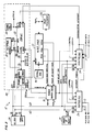
- Fig. 1 is an architectural block diagram of the multiplex communication system 10 for the body electrical functions of a vehicle and incorporating the present invention.
- the word “multiplex” will often be expressed as “Mux” and a remote multiplexer will be referred to as a "Remux”.
- the designations for various signals appearing on various conductors or at various ports in the system will be represented by descriptive abbreviations.
- the logic employed in the illustrated embodiment uses, in many instances, the "active-low" state of a signal for effecting some result.
- the multiplex communication system 10 employs a Mux computer 12 located at a central station within an automotive vehicle for providing control to and interacting with one or more remote multiplex (Remux) controllers 14 positioned at various remote locations about the vehicle.
- a Mux computer 12 located at a central station within an automotive vehicle for providing control to and interacting with one or more remote multiplex (Remux) controllers 14 positioned at various remote locations about the vehicle.
- Remux remote multiplex
- Communication between the Mux computer 12 and the Remuxes 14 is afforded via a four wire bus 15 which includes a first wire 16 for carrying bidirectional, serial, time division multiplexed data, a second wire 17 for conveying the serial multiplex clock (MUXCLK), a third wire 18 for extending a +5 volt DC supply voltage to the Mux computer 12 and the Remuxes 14 and a fourth wire 19 which serves as a signal ground (GND) for the multiplex system 10.
- the five volt supply voltage and the ground may be supplied by and referenced to the conventional 12 volt battery (not shown) of an automotive vehicle via a 5 volt regulator 20.
- the multiplex communications bus 15 between the Mux computer 12 and the various Remux controllers 14 might in some applications be open ended with the Mux computer 12 being located at one end and the various Remux controllers 14 tapping in parallel "T" connection to the conductors 16-19 along the length of the bus, in accordance with an aspect of the present invention the bus 15 is formed as a loop which is terminated at its opposite ends or terminals by differing portions of the Mux computer 12 to provide increased integrity and security to the multiplex communication system 10 as will be hereinafter described.
- Provision of a communication bus 15 configured as a loop controlled at each end by the Mux computer 12 permits detection of various anomolies which may occur in the transfer of information, such detection being of a nature to identify one or more breaks in the bus 15 and to further provide for maintaining transmission integrity in the event of such line break.
- the Mux computer 12 located at the central station includes a standard microprocessor 22 operatively connected with a master Mux controller 24 and a monitor Mux controller 24'.
- the master Mux controller 24 (Master Mux) and the monitor Mux controller 24' (Monitor Mux) are each formed of custom LSI CMOS gate array circuitry and are identical in construction but differ somewhat in operation as a function of time and control mode.
- One end of the loop of multiplex bus 15 is connected to Master Mux 24 and the other end is connected to Monitor Mux 24'.
- the microprocessor 22 in the preferred embodiment is a 4 MHz Z80, such as the Mostek 3880, employing NMOS circuitry, but it will be understood that other microprocessors are similarly applicable.
- Memory 25 is also provided in conjunction with microprocessor 22 in the Mux computer 12, and typically includes a 1K CMOS random access memory (RAM) 26 and a 4K CMOS programmable read only memory (EPROM) 27 shown in Fig. 2.
- Mux computer 12 also includes oscillator and counter/timer circuitry, generally represented by the function block 28, for generating the system timing signals and for providing a "sleep mode" of operation to be described hereinafter in greater detail. Operative interconnection between the microprocessor 22, memory 25, oscillator and counter/timer 28 and the Master and Monitor Muxes 24, 24' is afforded by various control lines shown later in greater detail as well as by a data bus and an address bus, so designated, within the functional illustraton of Mux computer 12.
- Each Remux controller 14 is provided with significant logic capacity for "intellectual" interaction with the Mux computer 12, and typically includes provision for 16 inputs from various vehicle switches and 16 outputs to various vehicle loads, a typical switch input being that for on-off control of headlights and a typical output being a control signal for turning on or turning off the headlights. It will be appreciated that the switch inputs may derive from the need to control numerous diverse loads and functions and similarly, that the output signals will serve to control numerous diverse types of loads.
- the architecture of each Remux 14 is such that it is divided into halves, each half having eight inputs and eight outputs and having a separate address.
- Remux 14 one side of a Remux 14 is designated the A side and is provided with an even numbered address and the other side is designated the B side and is given an odd number address which is numerically 1 greater than the A side address.
- the outputs from Remuxes 14 to the various vehicle loads typically provide low voltage control signals to various control elements or buffers 30 which in return respond by connecting or disconnecting the vehicle 12 volt supply to the load being controlled.
- the multiplex communication system 10 employs a communications protocol illustrated in Fig. 5B for use in the data communications between the Mux computer 12 and the Remuxes 14.
- This data protocol is intended to enhance the integrity of the communications system through an efficient detection of communication errors and/or anomolies.
- a thorough description of this data protocol is contained in U.S. Application Serial No. 469,591 for Vehicle Multiplex System Having Protocol/Format for Secure Communication Transactions filed February 24, 1983 by William Floyd and assigned to the same assignee as the present application, and is incorporated herein by reference.
- each communication transaction on the Mux data line 16 of multiplex bus 15 includes seven characters or bytes of eight bits each, the first byte being a sync byte, the following three bytes comprising a command message from the master controller 24 consisting of an address byte, a command byte and a CRC error detect byte and the final three bytes comprising a reply message from a Remux 14 consisting of an address byte, a response byte and a CRC error detect byte.
- the system 10 as presently configured has the potential for controlling as many as 128 Remuxes 14, each having two separate addresses, it will be understood that usually far fewer Remuxes 14 are actually required, only two being illustrated in the Fig. 1 embodiment.
- the system clock (SYSCLK) for controlling the timing of the microprocessor 22 and various other elements of the Mux computer 12 is typically of 2.5 MHz and is provided by an RC oscillator 28 of conventional design. Further, a similar type of RC oscillator provides a 50 KHz source 30 which is divided by two in the initial stage of a multistage binary counter 32 to provide a 25 KHz clock signal which is used as the multiplex clock (MUXCLK). Inasmuch as the serial Mux data appearing on multiplex bus 15 is clocked at a 25 KHz rate, the period of each bit will typically be .04ms and the period of an eight-bit byte is 0.32ms.
- Interactions between the microprocessor 22, its program stored in EPROM or PROM 27, the data stored in RAM 26, and the Master and Monitor Muxes 24, 24' is conducted at a rate determined by SYSCLK.
- Interaction between the microprocessor 22 and the memory elements 26 and 27 is determined by conventional decode control logic 34 which additionally includes timer decode logic for providing certain control signals to timer circuitry and power control switch circuitry generally represented by the blocks designated 31 and 35, respectively in Fig. 2 to be described hereinafter in greater detail.
- the processor 22 is interrupt driven, a nonmaskable interrupt (NMI)* being provided by the timer 31 at approximately 20 ms intervals.
- the hardware timer 31 includes two, eight-stage, divide-by-256 counters, 32 and 33, respectively of Fig. 3B.
- a timing signal occurring at 20 ms intervals from the timer 31 is applied to pulse generating circuitry, generally designated 36 in Fig. 2 for providing the NMI* signal. Additionally, upon initial powering-up of the multiplex system 10, as by connecting of the vehicle's battery cable, a conventional power up reset signal PUR1 is generated by conventional circuitry represented by block 37. This PUR1 signal may also be applied to the pulse generating circuitry 36.
- processor 22 utilizes eight bidirectional data lines D0-D7 for the parallel output and input of data to the memory elements 26, 27 and the Master and Monitor Muxes 24, 24'.
- the processor also includes 16 address lines A0-A15 for providing addressing signals to the memories 26, 27 and Master and Monitor Muxes 24, 24', as well as to the decode control logic 24.
- the data bus between processor 22 and the Master and Monitor multiplexers 24, 24' is designated 40 and the corresponding address bus between those elements is designated 42 and consists of A0-A9.
- Five further signal lines are provided at the processor 22 and at the Master and Monitor multiplexers 24, 24', and are designated RD*, WR*, IORQ*, Ml*, and INT*.
- the RD* signal is issued by processor 22 when it wishes to read data from memory 25 or an I/O device such as the multiplexers, 24, 24'. Depending on which is addressed by processor 22, one or the other of the multiplexers 24, 24' is issued the RD* signal to gate data onto the data bus 40 from multiplexers 24, 24'.
- the WR* signal provided by processor 22 indicates that the data bus 40 holds valid data to be stored in the addressed memory 26, 27 or I/O device multiplexers 24, 24'.
- the IORQ* signal indicates that the address bus 42 contains a valid I/O address for an I/O read or write operation. This signal is also generated with an Ml* signal when an interrupt is being acknowledged to indicate that an interrupt response vector can be placed on data bus 40.
- the Ml* signal indicates that the current processor cycle is the OP-Code Fetch cycle of an instruction execution, and it also occurs with IORQ*, as mentioned, to indicate an interrupt acknowledge cycle.
- the INT* signal is one generated by a multiplexer operating in its Master Mode, as Master Multiplexer 24, and is directed to processor 22 when an interrupt is being requested. This request is honored by processor 22 at the end of the current instruction being executed by the processor.
- the processor 22 issues a further control signal designated MREQ* which is extended to the RAM and EPROM decoding circuitry and to the NMI* pulse generator for selecting either ROM or RAM when the address holds a valid address for a Memory Read or Memory Write operation, and enabling the NMI* generator to provide a pulse for the NMI* input.
- MREQ* further control signal
- Master and Monitor Multiplexers 24 and 24' each include address input lines ADDCMP 1-7 for fixing or hardwiring their respective addresses.
- ADDCMP 1-7 address input lines
- All of the ADDCMP 1-7 inputs are tied to ground (logic 0) except for ADDACP 4 which is at +5 volts (logic 1).
- ADDCMP 4 is a logic 0
- input ADDCMP 5 is a logic 1. Accordingly, the Master and Monitor Muxes 24, 24' are separately identified and identifiable in their respective communications with processor 22.
- Each of the Master and Monitor Mux modules 24, 24' also includes an input designated MR which receives a signal designated PUR2 obtained in a manner to be hereinafter described and which effects a resetting initialization of the internal control registers and timing of the respective Muxes 24, 24'.
- the processor 22 scans the various Remuxes firstly to establish what, if any, input switches have been actuated, and secondly to effect the requisite output control action to the appropriate loads.
- the processor 22 which typically provides and receives operating addresses and data in a parallel manner, utilizes the Master Multiplexer 24 to convert the address and command issued to the respective Remuxes 14 into a serialized data format and to reconvert the serialized address and response data issued by the Remuxes 14 into a parallel format for transmission on the parallel data bus 40 to processor 22.
- a typical transaction between the Mux computer 12 and a Remux 14 includes, as illustrated in the trace of Fig. 5B, the issuance of a sync byte followed by an address byte, a command byte and an error check (CRC) byte in the message sent from the Master Mux 24 to a particular Remux 14. Subsequently the addressed Remux 14 will, or should, reply on Mux data line 16 with an address byte, a response byte and an error check (CRC) byte.
- the address byte sent by the Master Mux 24 contains the address of a selected half of one of the Remuxes 14.
- the command byte instructs the addressed Remux to respond with various input signals which it may have received by the actuation of outside switches and/or to provide output control signals to the output load devices connected to that particular half of the Remux.
- a cyclical redundancy error checking technique utilizes the address and command bytes for generating an error check byte which is transmitted to the addressed Remux.
- the Remux 14 which responds is presumably that which was addressed by Master Mux 24 and the response is initiated with an address byte which indicates the address of the particular responding Remux. That byte is followed by a response byte which indicates the response taken by the particular Remux to the received command message; typically revealing the status of various input switches and actuation of output loads.
- the status of switch inputs and/or output loads is typically determined by sampling latched switch inputs and actuation responses of load outputs.
- the response byte will typically also include an indication of whether or not the particular Remux, having done its own error checking of the incoming message from Master Mux 24, "agrees" with its error check byte.
- the error check byte sent by the Remux 14 will have been calculated using a CRC technique using its Address and Response in the reply message.
- the Multiplexer does its own error checking on the Remux Reply. Following each such transaction there may or may not be a period of bus latency in which all "ones" are written while a further instruction is awaited from processor 22.
- Fig. 4 the Master and Monitor Muxes 24, 24' are considered in greater detail. Because both are of identical architecture, they are discussed and illustrated as one in Fig. 4, though they are capable of functioning differently from one another in accordance with the invention. Accordingly, the discussion will first be from the standpoint of the Master Mux 24 and subsequently the Monitor Mux 24'. Further in Fig. 1 the bus 15 and its MUX DATA line 16 and MUXCLK line 17 are each shown with arrows at both ends, the solid arrowheads depicting the general flow in the presently discussed and illustrated configuration, and the dotted arrowheads depicting the reversed configuration.
- the programming of the control register 46 for the Master Multiplex function includes setting bit number 4 to a 1 to reset the internal logic in the Mux module. Once completed, bit number 4 automatically resets itself. Bit number 2 of register 46 is set to a 1 to enable the next byte on Data Bus 40 to be written into the Vector Address Register 50. Once completed bit number 2 automatically resets itself. Bits number 0, 1 and 3 must be set to 1 for the Mux to operate as a master. Specifically, if bit number 0 is a 1, the device is a master, otherwise it is a monitor. With bit number 1 as a 1, the Mux clock, MUXCLK, is transmitted on line 17 of bus 15. With bit number 3 as a 1, the Interrupt Logic 52 is enabled. Bit numbers 5, 6 and 7 may be programmed to any state since they are not used.
- Control Register 46 Following programming of Control Register 46 such that the device 24 will act as a Master Mux, it is again addressed by processor 22 and the multiplexing operation is initiated by writing the appropriate data byte (Address byte) into the Multiplex Register 54.
- A0 a logic 0, and data is entered in the register during a write, WR, operation.
- Master Mux 24 will start transmitting the SYNC character or byte (00010110) on the serial bus 16.
- the SYNC byte is derived from a SYNC Register 56.
- Synchronization of the SYNC byte and the subsequent data bytes transmitted by Master Mux 24 is effected by a conventional synchronization circuit 58 receiving a synchronization control signal SYNC, from counter logic 60 which responds to the 25 KHz Mux CLK for providing the appropriate phasing to the SYNC signal.
- SYNC synchronization control signal
- the Address byte stored in register 54 will be converted from parallel to serial by register 62 and is then automatically appended to the SYNC byte on the serial bus via synchronizing circuitry 58.
- An interrupt, INT* is then generated.
- the interrupt signal INT* is requesting that the processor 22 stop its existing action and service the MUX 24.
- a TINTRQ signal from the counter logic 60 is applied to Interrupt Decision logic 64 and being extended therefrom as an interrupt request signal to the Interrupt Register and Logic 52 for extension as signal INT to the processor 22.
- MI* and IORQ* Sometime after an interrupt is requested by the Master Mux 24, the processor 22 will send out an "interrupt acknowledge" (MI* and IORQ*).
- MI* and IORQ* "interrupt acknowledge"
- the Interrupt Logic 52 of Master Mux 24 will detemine the highest priority device which is requesting an interrupt. This is simply the device with its interrupt enable input, IEI, at a logic 1 and its interrupt enable output, IEO, at a logic 0. It will be noted in Fig.
- the Interrupt Logic 52 is such that when IEI is a logic 1, no other devices of higher priority are being serviced by an interrupt service routine from the processor 22. Additionally, the IEO signal from the Interrupt Logic 52 will be a logic 1 only if the IEI input to that Mux is a logic 1 and the processor 22 is not servicing an interrupt from that multiplexer.
- the processor 22 when the processor 22 is servicing an interrupt from that multiplexer, its IEO signal is a logic 0 and will serve to place the IEI inputs of other multiplexers to which it is connected to a logic 0, thereby making them subservient in the priority of interrupt servicing.
- Multiplex devices are inhibited from changing their interrupt request status when Ml* is active (0).
- the higest priority device places the contents of its Interrupt Vector Address Register 50 onto the data bus 40 during "interrupt acknowledge". After an interrupt by the Master Multiplex is acknowledged, that multiplexer is "under service”.
- the processor 22 When the processor 22 receives the interrupt, it has one byte time (.32ms) in which to write the Command byte into the Multiplex Register 54. If this time has elaspsed before data is written into the register 54, the data on the serial bus 16 following the Address byte will be nonvalid. As was the case with the Address byte, the Command byte will be transferred from register 54 through parallel to serial converter register 62 for output to the serial data line 16 via the data multiplexing sync circuit 58, the CRC data Mux gate 66 and the transmitter circuitry 68.
- serial Address and Command data bytes are being read from register 62 onto the serial data line 16, they are also being provided on the line designated "SDATA#2" to an input of an EXCLUSIVE OR gate 70 having its output connected to an input stage of CRC calculator register 72.
- the other input to the EXCLUSIVE OR gate 70 is provided by a selected one of the output stages of the CRC register 72 to perform the CRC calculation function in accordance with the description provided in the aforementioned application Serial No. 469,591.
- the CRC byte will have been generated in register 72 and is serially read therefrom and through the CRC Data Mux circuit 66 which has been enabled by a CRC word select signal CWS from the counter logic 60.
- the Master Mux 24 Upon completing the transmit mode, the Master Mux 24 automatically switches into the receiver mode. In the receiver mode, the Remux Address byte will be the first character to be received, after which an interrupt will be generated to signal the processor 22 that it is time to read that byte. Once again the processor has .32ms in which to read the byte, after which the byte is no longer valid.
- the data being received from line 16 by Master Mux 24 first enters through receive buffering circuitry 74 and is gated through logic circuitry 76 to the serial to parallel register 62.
- a transmit/receive control signal TNRECNTL applied to gate circuit 76 provides for the received data, R DATA, to be passed to serial to parallel register 62 and also provides that that data be extended to an input of the EXCLUSIVE OR 70 for use in the calculation of a CRC byte during the receive mode.
- the second byte will be the Remux response byte and it will be received in the same manner as the remote address byte. It too will signal the processor 22 with an interrupt indicating that valid data can then be read.
- the final byte received by Master Mux 24 will be the Remux's CRC byte. This byte will be compared to the byte generated by the CRC calculator 72 from the incoming data stream during the receive mode. If the two bytes compare, bit number 0 in the Master Muxes status register 78 will be a 0, whereas if the two CRC bytes do not compare bit number 0 in register 78 will be a 1. Also, an interrupt is again generated to signal the processor 22 that the status register should be read. Reading the status register 78 serves to reset that register.
- the state of bit number 1 will be indicative of operation in the transmit or the receive mode
- the state of bit number 2 will be indicative of the correctness or incorrectness of the CRC comparison if the device is operating in the monitor mode as will be discussed hereinafter.
- the state of bit number 3 signifies whether or not the Master Mux and Remux addresses compare when the device is operating in the monitor mode as will be described hereinafter and the state of bit number 4 is used to signify when a transaction has been completed.
- the Master Mux 24 When the status register 78 has been read and reset, the Master Mux 24 will switch back to the transmit mode and will send ones onto the serial bus 16; thus waiting for a write, WR*, from the processor 22 to initiate another transaction.
- Figs. 5A-L further correlates the timing of the above-described functions with the various parts of a complete transaction performed by Master Mux 24. It will be noticed in 5K that a single interrupt is generated during the transmit mode, whereas three separate interrupts are generated during the receive mode. It will also be noticed that the control signal DLOAD in 5E for loading parallel data into the parallel to serial register 62 occurs at the beginning of the address, command and CRC bytes respectively during the transmission mode, whereas hat function to convert from serial to parallel occurs at the end of the address, response and CRC bytes during the receive mode. The determination of whether or not the CRC byte received by Master Mux 24 was correct is determined by the signal CRC OK?
- a Master Address/Receive Address comparison signal M/RCOMP? occurs at the end of the receipt of the Remux address during the receive mode of the transaction; however, this function is performed only by Monitor Mux 24' as will be discussed hereinafter.
- the monitor mode may be attained either upon power-up initialization or by writing a 0 into bit numbers 0 and 3 of the control register 46.
- the multiplexer functions only as a receiver or listener, and interrupts to the processor 22 are never generated.
- the INT* is tri-state.
- an output line designated bus listen control BUSLCNTL from the bit number 0 position of control register 46 serves to control Master/Monitor select circuitry 80 for generating a control or gating signal MONLY which is a 1 when the device is to operate as a Master Mux and is a 0 when it is to operate as a monitor.
- MONLY control signal is extended to those portions of the Master/Monitor Mux circuitry which are to provide different modes of operation depending upon whether the chip is configured as a master or as a monitor.
- the device When configured as a Monitor Mux 24', the device operates only as a receiver and therefore is in the "sync search" state awaiting receipt of a Sync byte at the "downstream" end or terminal of the serial data line 16.
- the Monitor Mux When the Sync byte is received, it is recognized by Sync Detect Logic 63 and the Monitor Mux is initalized for enabling the following three bytes on the serial bus to be acknowledged.
- the first byte received after the Sync byte is the Remux address transmitted by the Master Mux. This byte is stored in the data buffer, MUX Data Register 54, for comparison later with the address byte sent by the responding Remux 14. Further, that first byte is gated through the CRC data Mux 76 and EXCLUSIVE OR gate 70 to the CRC calculator 72.
- the next byte received is the command from the Master Mux 24 and it also is gated through CRC data Mux 76 and EXCLUSIVE OR 70 into the CRC calculator 72 for determining a CRC byte value at the monitor.
- the third byte received by monitor 24' will be the Master's CRC.
- This CRC byte is also conducted through the CRC data Mux 76 and the EXCLUSIVE OR 70 to the CRC checker 72 to determine whether or not the CRC bytes compare. If the results are the same, bit number 2 in the status register 78 will be set to a 0 and if not, a 1 will be placed in bit number 2 of that register. After this operation, the CRC calculator 72 is automatically cleared.
- the fourth byte received by Monitor Mux 24' is the address byte sent by a responding Remux 14. This byte is compared to the Address byte previously sent by Master Mux 24 and presently stored in Mux data register 54. The comparison of the two address bytes occurs in Address Compare Logic 84 which is active only if the Mux chip is acting as a monitor 24'. If the two address bytes compare, bit number 3 of the Status Register 78 will be set to 0 and if not, a 1 will be place in bit number 3 of that register.
- Byte 4 received by Monitor Mux 24' is also passed through CRC data Mux 76 and EXCLUSIVE OR gate 70 into the CRC calculator 72 for use in determining a CRC byte.
- the fifth byte received by Monitor Mux 24' is the Response byte issued by the responding Remux 14. This response byte is directed through CRC data Mux circuit 76 and EXCLUSIVE OR gate 70 to the CRC calculator for determination of the CRC error byte.
- the sixth byte received by Monitor Mux 24' is the CRC byte sent by the responding Remux 14. This byte is also directed through CRC data Mux 76 and the EXCLUSIVE OR gate 70 for comparative combination with the CRC byte then stored in register 72.
- CRC byte transmitted by the Remux compares with that calculated in the Monitor Mux 14
- a 0 will be set in the bit number 0 position of the status register 78, but if the bytes do not compare, a 1 will be placed in the bit number 0 position of the status register.
- the SYNC search mode will be restored; thus enabling a new operation to begin.
- the processor 22 will instead interrogate the Monitor Mux 24' followin each transaction to ascertain whether or not the address and CRC checks performed by the monitor indicate accuracy, integrity and consistency in the transmissions between the Master Mux 24 and Remux 14. In the event errors are reflected by one or more of these checks, the processor 22 is capable of taking various forms of corrective action.
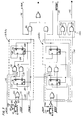
- a representative Remux 14 is illustrated in functional block diagrammatic form.
- the Remuxes 14 are provided by LSI gate array logic configured to provide the requiste functions discussed herein.
- Each Remux 14 is connected with the Mux bus loop 15 via parallel "T" connections with the respective four wires 16-19 of that bus. The provision of +5 volts and ground is not shown but is implied.
- the bidirectional data line connecting Remux 14 with the Mux data line is designated 16' and the line connecting the Remux with the MUXCLK line 17 is designated 17'.
- Appropriate circuitry 120 is located in line 17' for buffering the received MUXCLK. Similarly, in line 16' there is provided Receive buffering circuitry 121 and Transmit buffering circuitry 122 connected in complementary relationship. The incoming data on line 16' and the MUXCLK on line 17' are supplied as inputs to an eight bit serial-to-parallel and parallel-to-serial shift register 125 which is responsible for providing the appropriate conversions of data from one form to the other in response to an appropriate control signal CRTL. As used in the description of Fig. 6, the control signals CRTL are provided by control logic 128 and may provide a variety of control functions. The following discussion is intended to reveal the characteristics of those various control functions.
- Each of the Remuxes 14 on the Mux bus 15 awaits receipt of a Sync byte from the Master Mux 24 as an indication of a transaction to follow which may or may not be addressed to a particular Remux 14.
- the Sync byte is received on Mux data line 16' and entered in the register 125 where it is parallel connected via bus 130 to control logic 128 capable of recognizing the Sync byte pattern and providing a resulting control signal. Accordingly each Remux 14 is then synchronized to receive the next byte in the transaction from the Master Mux 24, that being an Address byte containing the address of a particular one of the Remuxes 14.
- Each of the Remuxes 14 will have a different preassigned address stored in address latch 132.
- the address latch 132 and the preprogramming of an address thereinto will be described later in greater detail.
- the address byte received on the serial data line 16' is compared by the Control Logic 128 with the Remux Address previously stored in address latch 132.
- the address for only one of the Remuxes 14 should compare and accordingly, the other Remuxes are effectively dormant for the remainder of that particular transaction. However, for the Remux 14 actually addressed, the bidirectional transfer of data will continue.
- the Command byte data may also be applied to the Control Logic 128 via bus 134 for effecting certain control actions, such as Read A Side A or B Side switches; Read Essential switches; and Diagnostic Byte.
- each Remux 14 is divided into halves, one half being designated the A side and the other half being designed the B side.
- a particular Remux 14 has a singular distinct address relative to all of the other Remuxes 14, the distinction between A side and B side within a particular Remux is determined by whether the least significant bit in the address is even or odd.
- An even LSB designates the A side of a Remux 14 and an odd LSB designates the B side of the Remux.
- Control Logic 128 Internal logic associated with Control Logic 128 is capable of determining whether the LSB is even or odd and thus the address latch 132 is only required to provide the seven more significant bits of the address.
- a resulting CRC value has then been determined in the calculator 138.
- the next byte to be received is a CRC byte transmitted by Master Mux 24 and it is introduced to the checking circuitry 138 via CRC data Mux 134 and the EXCLUSIVE OR gate 136 to determine whether the two CRC bytes compare. Unless they do compare, the Command byte previously received will not be executed.
- the execution of these commands requires converting the serial Command byte to parallel data applied via bus 130 to the Control Logic 128 so as to set certain A- or B-side latched outputs to a particular state or to condition the certain gating 142 such that it can transmit input switch states from either the A-side debounced switch register 144A, the B-side debounced switch register 144B or the essential switch register 146 to the parallel-to-serial register 125 via parallel bus 148. Further, a control signal CTRL from the Control Logic 128 may condition the register 125 to send a particular diagnostic byte.
- the Reply half of the handshake transaction between Master Mux 24 and Remux 14 begins with the Address byte identifying the particular Remux 14 and further, the A or B side thereof, which is responding.
- This address is derived from the address latch 132 and Control Logic 128 and is parallel loaded into register 125 for serial shifting out via serial line 150 which is extended through the transmit buffer 122 to the flux data line 16'.
- this reply transmission of the Remuxes address it is also entered into the CRC calculator 138 via CRC data Mux 134 and the EXCLUSIVE OR gate 136 in a manner before described.
- the response byte next sent by Remux 14 may be coded in a variety of ways to indicate the response taken by the Remux to the previously received command byte.
- each bit of the eight bit Response byte will signify and an input state of a respective one of the eight input switches.
- Each of the responses to each of the remaining commands discussed above is a uniquely coded eight bit byte indicative of a positive acknowledgement that a commanded output action has been effected.
- the output latches are monitored to determine that they were set to the state commanded and a coded Response byte indicating compliance is then formulated and transmitted.
- the Response byte is formed in shift register 125 and is serially shifted out on line 150 for transmission on line 16'.
- the response byte is entered in CRC calculator 138 for determination of a Reply CRC byte.
- CRC calculator 138 Upon formulation of that CRC byte, it is parallel shifted via bus 152 gating logic 142 and bus 148 into register 125 for serial transmission via line 150 to the Mux data line 16'.
- the transaction Upon completion of transmission of the CRC byte from Remux 14, the transaction is completed and the Remux returns to a state in which it awaits another sync byte and more specifically its address from the Master Mux 24.
- the Remux 14 is of course provided with power-on resetting circuitry (not shown) for initializing the circuitry each time it is powered up.
- FIG. 6 A facet of the invention is illustrated in Figs. 6, 7, and 8 concerning the provision of switch input signals to a Remux 14. It will be noted in Fig. 6 that MUXCLK received on line 17' is extended, after frequency division of 128 by divider 137 via internal line 17'' to the A side debounced switch register 144A and the B side debounced switch register 144B.
- Each of the registers 144A and 144B includes eight synchronously clocked debouncer circuits adapted for receiving inputs from single-throw switches and providing debounced signals to the remaining circuitry of the Remux for transmission during a response byte.
- Fig. 7further illustrates one of the essential switch inputs 1461 contained in the essential switch register 146.
- the individual debouncer circuits for the A and B side registers 144A and 144B are designate 144A1 and 144B1, respectively. Because the debouncing circuitry 144B1 associated with each of the B side switches is identical with that of the A side switch debouncers 144A1, only the latter will be described in detail. In those situations employing a single throw switch for input of a control signal to a digital logic system and particularly a logic system which is synchronously clocked, it is often advantageous to "debounce" the resulting signal in order to prevent an inaccurate indication of multiple switch opening and closings upon a single switch actuation.
- the debounced circuitry A1 is particularly suitable for detecting actuation of a single or multiple pole single throw switch and providing a clean, debounced synchronized signal for use by the internal circuitry of Remux 14 or other similar circuits.
- One terminal 161 of single-throw switch 160 is connected to ground (logic 0) and the other terminal 162 is connected through input buffer 163 to an input port of EXCLUSIVE OR 164.
- a positive voltage of 5 volts is applied to the input terminal 162 via resistor 166 to hold the input side of switch 160 at a logic 1 during its normally-open configuration. It will be appreciated, however, that the debouncer circuitry 144A1 is equally suitable with a single-throw switch of normally-closed configuration.
- the other input to EXCLUSIVE OR gate 164 is provided via line 168 from the Q output of a latch, such as D-flip-flop 170.
- EXCLUSIVE OR 164 is extended via line 171 to respective inputs on NAND gate 172 and AND gate 174.
- the MUXCLK signal supplied to the Remux on line 17' is processed via control logic 128 to provide an ACLK signal and an ACLK* signal operative in 180 o phase relationship during interrogation of the A side inputs, and a BCLK and BCLK* signals operative in 180 o relationship during interrogation of the B side inputs.
- the ACLK signal is applied via line 175 to another input of NAND gate 172.
- a third input to NAND gate 172 is provided via line 176 from the Q output of latch 178.
- AND gate 174 is provided from the Q* output of a latch, such as D-flip-flop 178, via line 179.
- the output of AND gate 174 is extended via line 180 to the D-input of latch 178.
- the ACLK* signal is extended via line 181 to the CLK input of latch 178.
- the output of NAND gate 172 is extended via line 184 to the CLK input of latch 170, the Q* output of that latch being connected via line 185 to its D-input.
- an optional preset signal may be applied via line 186 to the Asychonrous Clear (AC) inputs of the latches 170 and 178.
- AC Asychonrous Clear
- a debouncer circuit 144A1 with particular reference to the timing diagram of Fig. 8 which illustrates the signal waveforms at various locations throughout the circuit.
- the timing waveforms in Fig. 8 are designated according to the numbering in Fig. 7 of the signal line or component on which or at which they appear.
- the input from switch 160 appearing at terminal 162 is illustrated as normally being high until switch actuation, whereupon it goes low; however, due to bounce there are several alternations between the high and low logic states for an interval designated T B .
- the input signal 162 is applied to EXCLUSIVE OR gate 164 as is the resulting debounced output signal 168.
- the output 171 from EXCLUSIVE OR 164 is the logic 0 and no changes occur in the latches 178 and 170. If the two inputs signals to EXCLUSIVE OR gate 164 differ, the output 171 from EXCLUSIVE OR gate 164 is a logic 1. If the signal on line 171 is a logic 1, latches 178 and 170 may change state if the duration of the differing signals at the input of EXCLUSIVE OR gate 164 exceeds a capture time window equal T DB plus T A for the circuit.
- T DB of the capture time window represents the interval or period between successive down-steps in the ACLK signal.
- the expression T A for the capture time window represents that variable interval between the initial down-step in the switch input signal 162 occurring upon initial switch actuation and the next down-step in the ACLK signal (or up-step in ACLK*).
- the ACLK signal is a debouncer clock derived as mentioned from the transmitted MUXCLK such that its falling edge, or down-step, is time-synchronous with the system MUXCLK edge at which input data is desired to transition.
- the Q output 168 of latch 170 will toggle due to a clock signal 184 then appearing on its CLK input. This will result in the output 171 of the EXCLUSIVE OR gate 164 then returning to 0 since the Q output 168 of latch 170 is then the same logic state as the switch input signal 162. In any event, the Q output 176 of latch 178 will toggle to a 0 when clocked by the second ACLK* pulse following switch actuation, and in conjunction with AND gate 174, will set up to detect the next change in the switch input signal 162.
- next change will be an opening of the switch 160 to return signal 162 to a logic 1; however, the interval until that event will typically be determined by the construction of the switch and the duration of its actuation. For instance, although the trace 162 of switch input illustrates the switch opening after only several ACLK periods, it will be appreciated that it may be longer if the switch is of the momentary type and the user continues to depress the switch. Still further, the switch may remain actuated when the user removes finger pressure, in which case the interval of actuation would continue until the switch is manually opened.
- the output 168 of debouncer circuit 144A1 is a clean, debounced input signal which may then be applied to logic such as AND gate 190 such that it may be gated to the remaining relevant portions of the Remux 14 by a gating signal 192 which is provided when an A-side input switch is being interrogated.
- logic such as AND gate 190 such that it may be gated to the remaining relevant portions of the Remux 14 by a gating signal 192 which is provided when an A-side input switch is being interrogated.
- the debouncing circuitry 144B1 for each of the B side switch inputs is identical to that just described.
- some of the input switches are associated with so-called "essential” functions.
- essential functions include exterior lighting such as head and tail lights, hazard flashers, keyless entry system, and various others.
- clock signals such as ACLK, BCLK, etc., which are required for the proper debounce operation and latching of input signals using only the debouncing circuitry of 144A1, 144B1. Therefore, those input switches identified as being “essential” will also be capable of providing their input via the essential switch register generally designated 146 in Fig.
- FIG. 6 an individual such essential switch register being illustrated in greater detail in Fig. 7 and designated 1461.
- the switch input signal 162 extending from a B side input switch in Fig. 7 is extended via line 194 to an essential switch register 1461, and more specifically to one input of a pair of NAND gates 195, 196 which are cross-coupled in a conventional manner to provide a conventional latching circuit.
- the other input to this latching register 1461 is a resetting signal, RSTESW* provided via line 197 for resetting the latch following its interrogation.
- the output signal from the essential switch latch 1461 appears on lead line 198 where it is held following switch actuation and awaiting interrogation.
- a further aspect resides in the provision of a technique and circuitry for the automatic self-addressing of integrated digital devices. More specifically, the self-addressing circuitry is particularly applicable to large scale integrated circuits where the package pins available for I/O are at a premium. In the embodiment of multiplex system 10 under consideration, such a situation exists in connection with the LSI gate array circuits which make up each of the Remuxes 14. Accordingly, provision is made for establishing the address in the address latch 132 of the Remux 14 illustrated in Fig. 6 using the same I/O ports as are used for the output signals from the A side latched outputs 140A.
- FIG. 9 there is illustrated in generalized form, circuitry for implementing a time-shared method of digital control output and variable address input on the same actual signal pins of an integrated circuit device, as for instance Remux 14. Assuming some number, N, of I/O pins 200 are provided for time-shared output of data and input of address, it is also necessary to provide one additional I/O pin 201 to serve as an Address Common bus as will be described.
- Conventional external power-on-reset circuitry comprised of resistor 202 and capacitor 204 generate a power-on reset signal POR which is a normal input signal to Remux 14 provided via a normal existing pin 206 for use, following squaring and inversion by inverter 208 as a reset signal 210 extended to various other portions of the integrated circuitry of Remux 14. Additionally, signal 210 is applied to the enable gate input of a tri-state device 212 having its input connected to ground (logic 0), and having its output connected via line 214 to the Address Common I/O pin 201. The inverted state of reset signal 210 is obtained on line 216 at the output of inverter 218.
- the group of A side latched outputs 140A each include eight latches individually designated 220, and the address latch group 132 includes seven address latches individually designated 222. Accordingly in Fig. 9 each D-flip-flop latch 230 for the A side outputs is shown grouped with a respective D-flip-flop address bit latch 232 within a dotted block designated 220, 222.
- Each function block 220, 222 also includes a respective transceiver comprised of a tri-stated inverting transmitter output circuit 240 and a nontri-stated inverting receiver input circuit 242 of conventional design.
- the Q* output of output latch 230 is connected as the input to the transmitter circuit 240, the output of which is connected to a respective one of the I/O pins 200 for extension via a respective lead to respective external load circuitry (not shown).
- the input to receiver circuit 242 is connected to the same respective I/O pin 200, its inverted output being connected to the D-input of address latch 232.
- the RESET* signal appearing on line 216 is connected to the power-on reset, PRST, input of each of the output latches 230 and to the clock, CK, input of each of the address bit latches 232.
- the RESET* signal on line 216 is also connected to the enabling gate of each tri-state device 240.
- each output latch 230 is supplied with a respective gating signal via a respective lead 250 from the interior logic of Remux 14.
- a clock signal is supplied to the clock input, CK, of each output latch 230 via respective clocking leads 252 from the interior circuitry of Remux 14.
- each diode to be used in establishing the address configuration will have its anode connected to a respective one of the I/O pins 200 and will have its cathode connected to a Common line 262 which extends from the Address Common pin out 201 to the cathodes of each of the other diodes 260 to be used in the address configuration.
- a separate resistor 264 is connected at one end to a respective one of the output pins 200 and at the other end to +5 volts (logic 1) for normally holding the I/O pin 200 at a logic 1 voltage level. Similarly, this logic 1 voltage will be applied to the anodes of those diodes 260 used in the selected address configuration.
- Tri-state circuit 212 is of known design and normally provides a high impedance on the address common pin 201 and line 262; however, when the RESET signal on line 210 is a 1, the tri-state device 212 is also active and applies a logic 0 level on the Address Common I/O pin 201 and line 262.
- reset inverter 218 is also low on its output line 216.
- the signal on line 216- is then effective to place the tri-state devices 240 in the high impedance or Z state, permitting the logic states appearing at the respective ones of the I/O pins 200 to be input through the respective receiver devices 242 and in addition initializes the output latch 230.
- the respective pull-up resistors 264 will maintain the pin at a logic 1 level such that a 1 is applied to the receiver circuit 242.
- the receiver circuits 242 invert their respective inputs such that the D-input of a respective address latch 232 will receive a logic 1 if a logic 0 appears on the respective input pin 200 and will receive a logic 0 if a logic 1 appears at that pin.
- the RESET* signal 216 When RESET signal 210 is a 0, the RESET* signal 216 will apply a rising edge to the clock, CK, inputs of each of the address latch 232 and result in these states latching the address bits received via receiver circuits 242.
- tri-state circuit 212 goes to the high impedance Z state and the RESET* signal on line 216 places the tri-stated transmitter devices 240 in the active condition, thereby returning the I/O pins 200 to their normal role as device output pins.
- the unidirectional characteristic of the signal diodes 260 used in the selected address configuration serves an isolation or steering function which prevents logic states on any of the I/O pins 200 which happen to have addressing diodes 260 installed thereto from affecting each other via the Address Common line 262.
- Remux 14 Having completed a consideration of the circuitry of Remux 14, it is appropriate to further consider the interaction of processor 22, Master Mux 24, Monitor Mux 24' and, via serial bus 15, the Remuxes 14. Because the system 10 includes a pair of selectable, redundant multiplex controllers 24, 24' under the direction of a processor 22 in its Mux computer, the system is provided with enhanced integrity and operability. Firstly, the control program of the processor 22 is established such that it configures the Master and Monitor status of the Muxes 24, 24' to best ensure MUX DATA and MUX CLK transmission to and from the intended Remux 14.
- one of the redurdant Mux controllers is designated a Master and the other is designated a Monitor; however, their relative functions and designations may be reversed in the event the configuring program deems it desirable to effect the communications objective of the system.
- the Mux computer 12 is capable of recognizing this situation and reconfiguring or reversing the functional roles of the Master and Monitor Muxes 24, 24'.
- FIG. 11 the decisional process of processor 22 in configuring the Muxes 24 and 24' as Master and Monitor or Monitor and Master, respectively, is depicted in flow diagram form.
- the decisional and control process of processor 22 in determining whether or not a transmission using a particular Mux as a Master is "good” or "bad” is depicted in flow diagram form.
- the initial conditions for entering the "configuring" routine include either the power-up initialization step 300 which occurs when power is first applied to the total system or a request for configuration provided as a result of step 400 in the flow diagram of Fig. 12.
- step 302 obtains the address of the first Remux to be addressed in a predetermined sequence of Remux addressing.
- the control registers of the Muxes 24, 24' are set such that a preselected one, i.e., Mux 24, is a Master and the other, i.e., 24' is the Monitor. Absent a need to reconfigure, i.e., due to multiplex line degradation, this relationship will continue to be maintained.
- Step 306 then effects transmission of data to and from the addressed Remux via the selected Master Mux 24.
- Decision block 308 broadly represents one or more tests for determining the integrity and success of the communication transaction. Assuming that integrity is established, a flag 310 is set in the processor's memory which indicates that transmissions addressed to that particular Remux should continue to use multiplexer 24 configured as a Master to effect those transactions. On the other hand, if the integriy determination step 308 results in a negative decision, the effort to accurately complete the transaction to the addressed Remux via the initially selected Master Mux 24 will be repeated some number of times, N, as represented by block 312, and decision block 314 monitors whether or not the repeated attempts are successful. If an attempt is successful (Yes), the program routine returns to the affirmative output of block 308.
- the control program of the processor will reverse the relative roles of the Master and Monitor multiplexers such that the multiplexer 24 becomes the Monitor and the multiplexer 24' becomes the Master, as represented by block 316.
- This reversal of functions is effected by reversing the logic states of the relevant bit sent to the relevant stage of the control registers of the respective Muxes.
- the processor program will try as many as N times to direct communications to and from the Remuxes 14 through the former Monitor, now Master, Mux 24'.
- Decision block 320 determines whether or not this effort through the reconfigured arrangement of the Muxes is successful and assuming it is, the conclusion of block 322 is that a line break or the like has prevented the Mux computer from addressing the particular Remux through original Master 24 and must now address that Remux using Mux 24' as the new Master.
- Block 322 will set flags in memory so as to indicate a line break and to thereafter direct communications with that particular Remux through Mux 24' configured as a Master. If however, the decision of block 320 was negative, that particular Remux will thereafter be configured out of the system of possible Remux addresses, as represented by block 323.
- Block 324 asks whether all valid Remux addresses have been configured and if not, an instruction is issued by block 326 to get the next Remux address and the routine then returns to the entry point to block 304. When all Remuxes have been configured, the configuring routine is stopped.
- Step 350 provides for reading the Status Registers in both the Master and the Monitor Muxes 24, 24'. Based on that information, numerous decisions can then be made.
- block 354 determines if the CRC at the Master from the Remux is valid. If that CRC is not good, as by failure of CRC's to compare, the routine branches to a decision chain which first determines at block 364 if the Address received by the Master and conveyed to processor 22 is hexadecimal FF, i.e., all 1's. Such a condition is an invalid address and usually exists only if the MUX DATA line 16 is open and thus pulled to a constant logic 1 level. If the Address is not FF, the "resend" count is incremented at 358 and the message is resent at 362 unless the resend count is a maximum.
- a Monitor status bit is checked at 366 to determine if the first half (i.e., Master transmit) CRC is bad. If it is not bad, the "message resend" routine 358-362 and 400 is pursued; otherwise a Monitor status bit is checked at block 368 to determine whether the second half (i.e., Remux reply) CRC is bad. If it is not, the "message resend” routine 358-362 and 400 is pursued; otherwise a Monitor status bit is checked at block 370 to determine if the addresses sent by the Master and by the Remux fail to compare.
- the Response received at the Master and conveyed to processor 22 is inspected at block 380 to determine if it is a hexadecimal FF. If it is FF, the "message resend" routine of 358-362 and 400 is pursued; otherwise the routine proceeds to decision block 382 to check whether the "line break” flag has been set in block 322 of the "configure” routine. If the "line break” flag has not been set, the routine moves to block 384 to see if the Monitor's "transaction done” status bit has been set. If it has been set, the next transaction sequence may proceed, as represented by block 386.
- the aforedescribed "good-bad transaction" routine serves to incorporate a number of integrity checks and provides for several attempts at resending a transaction before postulating that a line break exists and that reconfiguration of the Master and Monitor Muxes may be required.
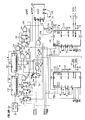
- Figs. 1, 2, 3A and 3B provision is made for operating the multiplex system 10, and particularly a portion thereof represented by the dotted block 500 in Fig. 2, in a low power mode for various intervals.
- the system's power source which typically is an automobile 12 volt storage battery
- the 50 KHz oscillator 30 is of conventional RC design and provides a 50 KHz signal to the clock input CK1 of an eight stage counter 32.
- the stages of the counter are connected so as to provide at its first Q A output the 25 KHz square wave signal which is extended to the Master and Monitor Muxes 24, 24' as the MUXCLK.
- the final Q D output of counter 32 is connected to the CK1 clock input of counter 33 to continue the ripple-down count provided by counter 32. It will be important to note, however, that the CL2 reset input for the second half of counter 32 and the CL1 reset input to the first half of counter 33 serve to reset those portions of the counters 32 and 33 and thereby change their count cycles when reset pulses are provided. Reset pulses are under control of processor 22 and usually follow NMI* pulses.
- the Q A output of the first stage of counter 33 is extended via line 510 to one input of an AND gate 512, the output of which is extended via line 514 to the CL2 reset input to the second half of counter 33.
- the Q C output of the third stage of counter 33 is extended via line 515 to one of the inputs of NAND gate 516, the output of which is extended to the D-input of D-flip-flop 518.
- the Q D output of the fourth stage of counter 33 is extended via line 519 to one input of AND gate 520 and to the CK2 clock input of the second half of that counter.
- the Q D output of the eighth stage of counter 33 is extended via line 522 to the input of an inverter 523 and also provides the reset signal, RESET. That RESET signal is extended through inverter 524 in Fig. 3A to provide the RESET* input to microprocessor 22 and to also provide signal PUR2 applied to the MR* inputs of Master and Monitor Muxes 24, 24'.
- the signal appearing on line 522 comprises one of the inputs to power control circuitry generally included within dotted enclosure 35.
- Power control circuitry 35 initiates and terminates the low power or "sleep" mode of operation.
- the power control logic 35 includes a D-type flip-flop latch 526, an AND gate 528 and finally a gated power switch such as MOSFET 530.
- the AND gate 516, D-flip-flop 518, D-flip-flop 532 and NAND gate 534 provide logic which, in conjunction with the counters 32 and 33, provides interrupt signals at 20ms intervals as will be hereinafter discussed, and genrally corresponds to pulse generator 36 in Fig. 2. Further, circuitry comprised of D-flip-flops 536, 538 and 540, as well as AND gate 542, serve to reset counters 32, 33.
- the D-flip-flop 518 will provide a nonmaskable interrupt signal, NMI* for controlling operation of the program for processor 22.
- the NMI* signal is first provided 20ms after the system is first powered and a power-up reset pulse PURl has occurred. Thereafter, NMI* interrupt signals will be generated at 20ms intervals during normal powered operation of the microprocessor 22.
- the NMI* signal is that transition occuring at the Q* output of flip-flop 518 when the first memory request signal MREQ* is applied to the clock CK input of the flip-flop following its D-input going to a logic 1 at 20ms intervals.
- That enabling of the D-input of flip-flop 518 at 20ms intervals is determined by line 515 from counter 33 and is conditioned upon the system being in its "on” or “awake” mode, as represented by the signal appearing on line 550 applied to the other input of AND gate 516.
- the MREQ* signal is also extended to the CK input of D-flip-flop 532 which has its D-input connected to the Q output of flip-flop 518.
- the Q* output of flip-flop 532 is provided as one input to NAND gate 534, the other input to which is provided by the Q output of flip-flop 518.
- a resetting signal coinciding with the NMI* pulse is provided on line 552 at the output of NAND gate 534 at 20ms intervals and continues until the next MREQ* signal.
- the reset signal appearing on line 552 is extended to the CL* input of D-flip-flop 536 which reenables the timer reset logic 538, 540 and 542.
- Flip-flops 538 and 540 are initially cleared by a power-up reset PURl upon initial application of power. Further, the Q* output of flip-flop 536 is set to a logic 1 by the signal appearing on line 552 following each NMI* signal. This action sets flip-flops 538 and 540 such that their Q* outputs connected to the input of NAND gate 542 are both set to 0 and 1 respectively when a 50 KHz clock is applied to their respective clock CK inputs. Accordingly, the output of AND gate 542 would then be 0 and would not effect a resetting of timers 32 and 33.
- TIMERST which is extended to the clock CK input of flip-flop 536 for toggling first that flip-flop and then the two subsequent flip-flops 538 and 540 such that the output of AND gate 542 goes to a logic 1.
- Such a logic 1 at the output of AND gate 542 then effects a resetting of the last four stages of counter 32 and the first four stages of counter 33.
- the TIMERST resetting signal is provided at approximately 20ms intervals and accordingly, the counter 33 is reset before it proceeds to the next count following its 20ms output from the third stage on line 515.
- the counters 32 and 33 will no longer be reset and will continue their normal ripple-down count. Under such circumstances the counter 33 will continue to count beyond the 20ms inverval at which it would normally be reset and will reach a time of 40ms which is reflected by a logic 1 appearing on line 519 applied to the input of NAND gate 520. If at that time the other input to NAND gate 520 is a logic 1, as will be the case during normal powered operation, the NAND gate will output a logic 1 signal which is extended via line 556 to the PR* input of latch 526 such that its Q output is set to a logic 1.
- the power MOSFET 530 is "on” and provides +5 V SW when its gate input is a logic 0, and is off when its gate input is a logic 1.
- the Q output of flip-flop 526 is extended via line 558 to the control gate of FET 530 such that when it goes to a logic 1, the FET is switched off and +5 V SW is disconnected from the circuitry 500.
- +5 V SW supply is disconnected from the microprocessor 22, the system enters a "power-down" or "sleep" mode.
- the counter 33 may then provide a reenabling or "wake-up” signal at some later time. Specifically, when the interval since the last NMI* interrupt reaches about 654ms, the final stage of the timer 33 will go to a logic 1 which is extended via line 522 to provide the aforementioned reset pulse RESET and to provide a wake-up signal to the input of inverter 523 in the power control circuit 35.
- Inverter 523 will then provide a 0 at the CL* reset input to latch 526, thereby resetting its Q output to a logic 0 which turns FET switch 530 "on” and reapplies power to the microprocessor 22 and other circuitry 500.
- the logic repeatedly tries to get the microprocessor 22 back into an operational mode after a "watchdog” event by first powering down and then repowering and, at the time of repowering, by extending a reset signal RESET to the processor to initialize it at each attempted restart.
- the processor 22 When and if the processor 22 is effectively restarted, it will resume generating TIMERST pulses to effect resetting of timer counters 32, 33 for inhibiting subsequent "watchdog power-down".
- the power control switch 35 has been discussed in association with the initiation of power-down in response to the watchdog circuitry timing out because no TIMERST resetting pulse occurred. However, that power switch 35 may also be used to power-down the microprocessor 22 and place it in a "sleep" mode in response to a control signal provided by the processor. Specifically, if it is desired to enter a "sleep” mode the processor 22 may generate a "power-down" or "power-off" strobe signal, PWRSTB, derived via the timer decode logic 34C. The PWRSTB signal is extended to the clock CK input of the power control latch 526.
- the processor 22 can place itself and the other circuitry within block 500 in the "sleep" mode such that all communications on the Mux Data line 16 are stopped and the MUXCLK signal on line 17 is turned off.
- the timing of the PWRSTB signal which initiates the "sleep” mode is pre-established to occur shortly after the issuance of a TIMERST pulse such that little or no time has elapsed since the timers 32 and 33 were reset. Accordingly, those timers 32, 33 will begin their timing at substantially the same time as the "sleep" mode is initiated by PWRSTB.
- the power control register 526 will reverse states and the FET power switch 530 will again be turned on to "wake-up” or "power-up” the processor 22 and the other circuitry within block 500.
- the power control switch 35 additionally provides, via the output of AND gate 528 and the inverter 566, a Chip Select signal CS* which is extended to the CS* inputs of Master and Monitor Muxes 24, 24'.
- CS* Chip Select signal
- the Muxes 24, 24' are prevented from accepting any signals from processor 22 and will place the MUXCLK signal on line 17 at a constant high level for its duration.
- the power switch circuitry 35 via the output from AND gate 528 and the NAND gate 568, will serve to inhibit the enabling of RAM 26 by RAM enable signals RAMENB applied to the other input of the NAND gate 568 so long as the system is in the "power-down” or "sleep mode". This provision is desirable inasmuch as the RAM 26 is not to be enabled during the "power-down” mode and there is a chance that the RAM decode circuitry 34B might inadvertently provide an enabling signal RAMENB at or during the "power-down” mode.
- the various "essential" body electrical functions previously mentioned are those which must function independently of the vehicles' ignition switch position. For example, lights (exterior, headlamps, hazard, etc.) must be operable at all times and are thus an "essential” function.
- windshield wipers only operate when the ignition switch is “on” in the"RUN” or “ACCESSORY” position and are thus a “nonessential” function.
- the multiplex system 10 is powered directly from the vehicles' battery rather than through the ignition switch because of these essential functions.
- the "sleep" mode provided herein serves to automatically reduce the power drain on the battery by the multiplex system during periods of inactivity, such as when the vehicle is parked.
- the "sleep" mode and the "essential" switch inputs 146 have been configured such that the multiplex system resonds to essential inputs within a reasonable time even though the system may have been in a "sleep" mode.
- the programmed processor 22 periodically looks at the ignition switch, as represented by flow diagram block 600.
- the ignition switch (or switches, if more than single “on” and “off") is connected to a B-side debounced input 144B1 of a Remux 14, and thus also is connected to an essential switch register 1461.
- Decision block 602 determines whether or not the ignition system is “off” and if it is not, the routine goes immediately to block 630 which tells the system to remain “on” or “powered-up” and to service the operator's commands. If the ignition system is "off”, the routine moves to step 604 which begins the "sleep" decision process.
- the first determination of the "sleep" decision process is whether the exterior light system or hazard light system (or other "essential” function), is "on”. If one is “on”, the routine goes to block 634 to remain “on”, but if none are “on”, a 10 second monitoring time period is provided during which the power is maintained, as represented by block 608. The 10 second monitoring period is measured by the program software. During the 10 second monitoring period the system inputs continue to be scanned, as seen in block 610, and decision block 612 determines whether or not any "essential" function or ignition switch has been activated during the 10 second monitoring interval. If so, the system continues to poll switches and service driver's commands, as represented at block 630, and the loop returns to block 600. If a switch has not been activated during the 10 seconds, the decision is made to enter the "sleep" mode at step 616.
- the "sleep" mode sequence first provides, at block 618, for all of the Remuxes 14 to be placed in their low power dissipation mode by setting their output latches 140A and 140B so as to deactivate the loads and by gating "off" the MUXCLK. Deactivating the loads puts the external electronic drives in the lowest power configuration. Gating "off” the MUXCLK puts the Muxes and Remuxes in the lowest power configuration due to the fact that CMOS power consumption is directly related to the number of gate transitions in the device.
- a power-off strobe pulse PWRSTB is generated by the software for extension to the power switch latch 526.
- Block 622 indicates that the PWRSTB pulse and latch 526 operate to switch "off” the +5 V SW power for the Mux computer circuitry in dotted box 500 in Fig. 2.
- the power for the circuitry in box 500 is timed to remain “off” for 654ms, with the dotted line path to block 624 representing that this timing is a hardware function and that power is switched back on at the end of the timing interval.
- the routine determines whether or not any "essential" switch activity occurred during the immediately preceding 654ms "sleep" interval. If such activity did not occur, the routine returns to block 620 to reenter the "sleep" mode. If, however, "essential” switch activity did occur, the routine proceeds to block 630 where it continues to poll switches and service driver commands. The routine then restarts the "low-power" decision at block 600.
Landscapes
- Engineering & Computer Science (AREA)
- Theoretical Computer Science (AREA)
- General Engineering & Computer Science (AREA)
- Physics & Mathematics (AREA)
- General Physics & Mathematics (AREA)
- Computer Hardware Design (AREA)
- Computing Systems (AREA)
- Selective Calling Equipment (AREA)
- Small-Scale Networks (AREA)
- Communication Control (AREA)
- Power Sources (AREA)
Claims (17)
- Système de commande pour conduire des transactions de données soumises à des impulsions d'horloge entre un poste de commande central (12) et une ou plusieurs unités de commande éloignées (14) reliées à celui-ci, constitué de moyens pour soumettre à des impulsions d'horloge ledit poste de commande centrale et lesdites unités de commande éloignées pour cette transaction de données, le poste de commande central comprenant des moyens de traitement électronique de signal (22), pour commander les transactions de données avec les unités de commande éloignées, et pour commander ledit comptage par horloge desdites transactions, le système de commande étant alimenté en puissance par une source de puissance électrique de capacité limitée, et ledit comptage par horloge des transactions de données consommant du courant au poste de commande central et aux unités de commande éloignées, caractérisé en ce qu'il comporte:
des moyens commutateurs de puissance (35) reliés fonctionnellement à la source d'alimentation et à une partie du système de commande pour relier de façon sélective ou interrompre ladite alimentation de la partie du système de commande, en réponse à des signaux de commande de connexion ou de déconnexion de l'alimentation respectifs
des moyens (34) pour fournir automatiquement un signal de commande de coupure d'alimentation (PWRSTB), en réponse à une condition prédéterminée d'inactivité du système,
des moyens de temporisation (31) en mesure de fonctionner comme un temporisateur réinitialisable continuellement par une horloge, les moyens de traitement fournissant un signal de réinitialisation périodique (TIMERST), ledit signal de réinitialisation étant relié fonctionnellement au temporisateur pour réinitialiser celui-ci, dans lequel le signal de commande de coupure d'alimentation (PWRSTB) est fourni par ledit processeur seulement un bref intervalle de temps prédéterminé après qu'un signal de réinitialisation soit émis par le processeur, de façon que ledit temporisateur démarre à partir d'une référence connue, le temporisateur (31) étant en mesure de fonctionner pour mesurer un intervalle de temps prédéterminé durant lequel l'alimentation est déconnectée de ladite partie du système de commande et pour produire un signal de commande d'alimentation (alimentation-temporisateur sommeil) à la fin dudit intervalle prédéterminé, aux moyens commutateurs (35), dans lequel le signal de réinitialisation normalement fourni par les moyens de traitement (22), alors que l'alimentation est reliée à ceux-ci, peut ne pas intervenir si le processeur fonctionne de façon incorrecte, dans lequel ledit temporisateur (31) fournit un signal de commande "chien de garde" (coupure alimentation-chien de garde) après un intervalle prédéterminé plus long que l'intervalle normal entre les signaux de réinitialisation issus du processeur vers les moyens commutateurs (35), pour couper l'alimentation de la partie du système de commande, dans lequel l'intervalle du signal de commande d'alimentation est plus long que le signal de commande "chien de garde", de façon que la puissance sait rendue à la partie du signal de commande, suivant la suppression de l'alimentation par un signal chien de garde,
des moyens de circuit de commande (526) reliés fonctionnellement aux moyens commutateurs de puissance (35) et étant liés au signal de commande de coupure d'alimentation, et le signal de commande de chien de garde fournissant ledit signal de commande de coupure d'alimentation pour déconnecter la source de puissance de ladite partie du système de commande et étant liés au signal de commande d'alimentation pour fournir le signal de commande d'alimentation pour connecter la source de puissance à ladite partie du système de commande, au moins une des unités de commande éloignées (14) étant reliée aux moyens d'entrée de données pour recevoir des données d'entrée (entrées commutateurs), et
des moyens de traitement de signal (22) contrôlant les données entrées vers au moins l'une des unités de commande éloignées, au travers des moyens d'entrée de données, en réponse à ces données entrées représentatives de ladite condition prédéterminée d'inactivité, ces moyens entrant un mode de commande de coupure d'alimentation pour produire un signal de commande contrôlé par horloge pour envoyer ce dernier au poste de commande central et le signal de commande de connection de d'alimentation. - Système de commande suivant la revendication 1 caractérisé en ce qu'au moins une des unités de commande éloignées reçoit des données d'entrée prédéterminées pour indiquer si ladite partie du système de commande demande ou non d'être alimentée en puissance, le signal de commande de coupure d'alimentation étant fourni par les moyens de traitement de signal central en réponse aux données d'entrée indiquant l'absence d'un besoin d'alimentation de cette partie de système.
- Système de commande suivant la revendication 2 caractérisé en ce que ledit système de commande, commande les fonctions électriques d'un véhicule et dans lequel les données d'entrée indiquent si ladite partie du système de commande demande ou non l'état du commutateur d'allumage et l'état d'unautre commutateur essentiel.
- Système de commande suivant la revendication 1 caractérisé en ce que les moyens de traitement de signal comprennent un processeur intégré et des moyens pour stocker un programme de celui-ci, à la fois le processeur et les moyens de stockage de programme étant compris dans la partie de système de commande duquel la puissance est déconnectable, et dans lequel le processeur fournit le signal de commande d'arrêt d'alimentation.
- Système de commande suivant la revendication 4 caractérisé en ce que les moyens de temporisation et les moyens de circuit de commande sont connectés continuellement à la source de puissance.
- Système de commande suivant la revendication 5 caractérisé en ce que le signal de commande d'alimentation provient du temporisateur dans un intervalle de temps après la coupure d'alimentation par le signal de commande "chien de garde", cet intervalle de temps étant d'une longueur telle qu'il diminue d'une façon significative la moyenne de consommation de puissance sans retarder, de façon significative, l'entrée des données fournies a une unité de commande éloignée.
- Système de commande suivant la revendication 6 caractérisé en ce que l'intervalle entre une coupure d'alimentation par un signal de commande chien de garde et le signal suivant de commande de mise en alimentation est d'environ 650 ms.
- Système de commande suivant la revendication 5 caractérisé en ce que les moyens de circuit de commande comprennent un verrou bistable réinitialisable prédéterminé pour répondre à l'impulsion de commande chien de garde de coupure d'alimentation pour fournir ledit signal de commande aux moyens de commutation, pour déconnecter l'alimentation de ladite la partie du système de commande, ledit élément bistable étant réinitialisé par le signal de commande de coupure d'alimentation pour fournir ainsi un signal de commande audit moyen commutateur pour connecter l'alimentation à ladite partie du système de commande.
- Système de commande suivant la revendication 5 caractérisé en ce que le processeur est attaqué en interruption, le temporisateur est un compteur descendant multi-étages, et comprend, de plus, des moyens de circuit logique alimentés de façon continue, reliés à un ou plus des étages sélectionnés dudit compteur et à un signal de demande provenant du processeur pour fournir des signaux d'interruption périodiques sensiblement à des intervalles déterminés par l'étage compteur sélectionné, ledit signal d'interruption étant envoyé au processeur pour réaliser l'exécution du programme de celui-ci.
- Système de commande suivant la revendication 9 caractérisé en ce que les moyens de circuit logique de signal d'interruption sont reliés de plus au signal de commande pour couper l'alimentation du processeur de façon à inhiber la production du signal d'interruption.
- Système de commande suivant la revendication 5 caractérisé en ce que le processeur est un dispositif intégré à grande échelle utilisant des circuits NMOS.
- Système de commande suivant la revendication 8 caractérisé en ce que le processeur est attaqué en interruption, le compteur de temps est un compteur descendant multi-étages et comprend des moyens de circuit alimentés de façon continue, reliés à un ou plus des étages sélectionnés dudit compteur et à un signal de demande provenant du processeur pour fournir des signaux d'interruption périodiques sensiblement à des intervalles déterminés par l'étage compteur sélectionné, ledit signal d'interruption étant envoyé audit processeur pour réaliser l'exécution du programme de celui-ci, ledit signal de réinitialisation périodique fourni par le processeur intervenant lorsque celui-ci est alimenté et fonctionne correctement et, comporte de plus des moyens de logique réinitialisables alimentés de façon continue, liés au signal de réinitialisation du processeur, pour appliquer ledit signal de réinitialisation pour réinitialiser le temporisateur, les moyens logiques de réinitialisation étant prédéterminés par les signaux d'interruption pour appliquer le signal de réinitialisation de façon à réinitialiser le temporisateur, l'absence desdits signaux d'interruption, lorsque l'alimentation est déconnectée du processeur, empêchant ainsi la prédétermination des moyens logiques de réinitialisation de façon à s'assurer que le temporisateur n'est pas réinitialisé.
- Système de commande suivant la revendication 8 caractérisé en ce que l'élément verrou est également préinitialisable et le signal de commande chien de garde est apte à réaliser la présélection de l'élément de verrou.
- Système de commande suivant la revendication 3 caractérisé en ce que les moyens de traitement de signal comprennent un processeur inrégré et des moyens pour stocker un programme dudit processeur, les moyens de stockage du processeur et du programme étant compris dans une partie du système de commande auquel la puissance est déconnectable, le processeur fournissant le signal de commande de coupure d'alimentation, et dans lequel le processeur attend l'issue du signal de commande de coupure d'alimentation pendant un intervalle fixé par programme de durée prédéterminée et continue à contrôler les données entrées pour tout changement qui pourrait annuler la délivrance du signal de commande d'alimentation.
- Système de commande suivant la revendication 14 caractérisé en ce que la durée du retard dans la production du signal de commande de coupure d'alimentation est d'approximativement 10 secondes.
- Système de commande suivant la revendication 3 caractérisé en ce que la commande centrale comprend une ou plusieurs unités de commande multiplex, les unités de commande éloignées étant reliées aux unités de commande multiplex par un bus série, ce bus série servant à envoyer les données multiplex et les signaux d'horloge multiplex des unités de commande multiplex vers les unités de commande éloignées, les unités de commande multiplex et les unités de commande éloignées étant constituées de circuits intégrés à grande échelle pour une opération multiplex, et dans lequel la déconnection de l'alimentation de ladite partie du système de commande intervient pour envoyer les signaux de données multiplex et d'horloge multiplex aux unités de commande multiplex et aux unités de commande éloignées, diminuant ainsi leur consommation de puissance.
- Système suivant la revendication 15 caractérisé en ce que l'entrée de données pour les unités de commande éloignées provenant de commutateurs considérés comme essentiels est stockée dans des verrous respectifs des contrôleurs éloignés, même lorsque l'alimentation est déconnectée, dans lequel les verrous sont interrogés à chaque reconnection de l'alimentation audit système, pour déterminer s'il faut converser l'alimentation ou de nouveau couper celle-ci.
Applications Claiming Priority (2)
| Application Number | Priority Date | Filing Date | Title |
|---|---|---|---|
| US06/540,582 US4698748A (en) | 1983-10-07 | 1983-10-07 | Power-conserving control system for turning-off the power and the clocking for data transactions upon certain system inactivity |
| US540582 | 1983-10-07 |
Publications (3)
| Publication Number | Publication Date |
|---|---|
| EP0140814A2 EP0140814A2 (fr) | 1985-05-08 |
| EP0140814A3 EP0140814A3 (en) | 1988-05-04 |
| EP0140814B1 true EP0140814B1 (fr) | 1993-08-04 |
Family
ID=24156064
Family Applications (1)
| Application Number | Title | Priority Date | Filing Date |
|---|---|---|---|
| EP84630152A Expired - Lifetime EP0140814B1 (fr) | 1983-10-07 | 1984-10-05 | Système de contrôle à conservation d'énergie |
Country Status (6)
| Country | Link |
|---|---|
| US (1) | US4698748A (fr) |
| EP (1) | EP0140814B1 (fr) |
| JP (1) | JPS60143050A (fr) |
| CA (1) | CA1229875A (fr) |
| DE (1) | DE3486192T2 (fr) |
| ES (1) | ES536542A0 (fr) |
Cited By (1)
| Publication number | Priority date | Publication date | Assignee | Title |
|---|---|---|---|---|
| US6114887A (en) | 1995-12-29 | 2000-09-05 | Intel Corporation | Apparatus for generating bus clock signals with a 1/N characteristic in a 2/N mode clocking scheme |
Families Citing this family (288)
| Publication number | Priority date | Publication date | Assignee | Title |
|---|---|---|---|---|
| NL8401557A (nl) * | 1984-05-15 | 1985-12-02 | Philips Nv | Rekenmachinesysteem met verwijderd opgestelde werkstations en een reservebatterijvoeding. |
| JPS61262827A (ja) * | 1985-05-15 | 1986-11-20 | Mitsubishi Electric Corp | 半導体集積回路装置 |
| US5245314A (en) * | 1985-09-18 | 1993-09-14 | Kah Jr Carl L C | Location monitoring system |
| CA1242809A (fr) * | 1985-12-20 | 1988-10-04 | Mitel Corporation | Systeme de stockage de donnees |
| US4851987A (en) * | 1986-01-17 | 1989-07-25 | International Business Machines Corporation | System for reducing processor power consumption by stopping processor clock supply if a desired event does not occur |
| JPS63163912A (ja) * | 1986-12-26 | 1988-07-07 | Toshiba Corp | マイクロコンピユ−タシステム |
| GB8701496D0 (en) * | 1987-01-23 | 1987-02-25 | Salplex Ltd | Information handling & control systems |
| JPH0695656B2 (ja) * | 1987-03-12 | 1994-11-24 | 株式会社東芝 | 無線チヤネルサ−チ方式 |
| JPS63248227A (ja) * | 1987-04-03 | 1988-10-14 | Aisin Seiki Co Ltd | 電話装置 |
| JP2516983B2 (ja) * | 1987-06-19 | 1996-07-24 | 松下通信工業株式会社 | 無線電話装置 |
| JP2760787B2 (ja) * | 1987-08-28 | 1998-06-04 | 株式会社日立製作所 | 電子計算機システムの運転制御装置 |
| DE3828745A1 (de) * | 1987-09-29 | 1989-04-13 | Pioneer Electronic Corp | Navigationsvorrichtung fuer ein kraftfahrzeug |
| US4812677A (en) * | 1987-10-15 | 1989-03-14 | Motorola | Power supply control with false shut down protection |
| WO1989006012A1 (fr) * | 1987-12-17 | 1989-06-29 | Rakoczy G Istvan | Procedure et equipement d'arret automatique de machines de traitement de donnees |
| US5051936A (en) * | 1987-12-21 | 1991-09-24 | Johnson Service Company | Microprocessor-based controller with synchronous reset |
| FR2626998B1 (fr) * | 1988-02-05 | 1990-08-03 | Bendix Electronics Sa | Systeme de mise en etat operationnel et en etat de veille de boitiers electroniques connectes a un canal de communication |
| US5524083A (en) * | 1988-03-31 | 1996-06-04 | Square D Company | Decentralized, modular tripping arrangement |
| JPH0759109B2 (ja) * | 1988-04-20 | 1995-06-21 | 日本電気株式会社 | 終話処理機能付自動車電話端末機 |
| US4965738A (en) * | 1988-05-03 | 1990-10-23 | Anton/Bauer, Inc. | Intelligent battery system |
| DK174975B1 (da) * | 1988-05-06 | 2004-04-05 | Toppan Printing Co Ltd | Integreret kredsløbskort |
| US5016196A (en) * | 1988-05-24 | 1991-05-14 | Battelle Memorial Institute | Rain sampling device |
| US5115513A (en) * | 1988-08-18 | 1992-05-19 | Delco Electronics Corporation | Microprogrammed timer processor |
| US4980836A (en) * | 1988-10-14 | 1990-12-25 | Compaq Computer Corporation | Apparatus for reducing computer system power consumption |
| JPH02148210A (ja) * | 1988-11-30 | 1990-06-07 | Toshiba Corp | フラットパネルディスプレイの着脱制御回路 |
| US5249298A (en) * | 1988-12-09 | 1993-09-28 | Dallas Semiconductor Corporation | Battery-initiated touch-sensitive power-up |
| US5203000A (en) * | 1988-12-09 | 1993-04-13 | Dallas Semiconductor Corp. | Power-up reset conditioned on direction of voltage change |
| US5175845A (en) * | 1988-12-09 | 1992-12-29 | Dallas Semiconductor Corp. | Integrated circuit with watchdog timer and sleep control logic which places IC and watchdog timer into sleep mode |
| US5590343A (en) * | 1988-12-09 | 1996-12-31 | Dallas Semiconductor Corporation | Touch-sensitive switching circuitry for power-up |
| US5754462A (en) * | 1988-12-09 | 1998-05-19 | Dallas Semiconductor Corporation | Microprocessor auxiliary with ability to be queried re power history |
| WO1990006552A1 (fr) * | 1988-12-09 | 1990-06-14 | Dallas Semiconductor Corporation | Mise en circuit a effleurement declenchee par batterie |
| US5073943A (en) * | 1988-12-27 | 1991-12-17 | Ford Motor Company | Automotive audio system having active controls in reduced power state |
| US5247164A (en) * | 1989-01-26 | 1993-09-21 | Hitachi Maxell, Ltd. | IC card and portable terminal |
| JPH02201516A (ja) * | 1989-01-31 | 1990-08-09 | Toshiba Corp | パワーセーブ方式 |
| US5018148A (en) * | 1989-03-01 | 1991-05-21 | Ncr Corporation | Method and apparatus for power failure protection |
| US5142278A (en) * | 1989-04-18 | 1992-08-25 | Qualcomm Incorporated | Current carrier tractor-trailer data link |
| US5155809A (en) * | 1989-05-17 | 1992-10-13 | International Business Machines Corp. | Uncoupling a central processing unit from its associated hardware for interaction with data handling apparatus alien to the operating system controlling said unit and hardware |
| US4952817A (en) * | 1989-05-31 | 1990-08-28 | Dallas Semiconductor Corporation | Self-starting test station |
| US5163153A (en) * | 1989-06-12 | 1992-11-10 | Grid Systems Corporation | Low-power, standby mode computer |
| US5241680A (en) * | 1989-06-12 | 1993-08-31 | Grid Systems Corporation | Low-power, standby mode computer |
| US5041964A (en) * | 1989-06-12 | 1991-08-20 | Grid Systems Corporation | Low-power, standby mode computer |
| DE69031807T2 (de) * | 1989-06-30 | 1998-04-09 | Fujitsu Personal Syst Inc | Methode zur Reduzierung der Leistungsaufnahme eines Rechners |
| US5222239A (en) * | 1989-07-28 | 1993-06-22 | Prof. Michael H. Davis | Process and apparatus for reducing power usage microprocessor devices operating from stored energy sources |
| AU629019B2 (en) * | 1989-09-08 | 1992-09-24 | Apple Computer, Inc. | Power management for a laptop computer |
| US5167024A (en) * | 1989-09-08 | 1992-11-24 | Apple Computer, Inc. | Power management for a laptop computer with slow and sleep modes |
| US5151855A (en) * | 1989-10-19 | 1992-09-29 | Saturn Corporation | Multiple microprocessor single power supply system shutdown |
| US5218704A (en) * | 1989-10-30 | 1993-06-08 | Texas Instruments | Real-time power conservation for portable computers |
| US6158012A (en) * | 1989-10-30 | 2000-12-05 | Texas Instruments Incorporated | Real-time power conservation and thermal management for computers |
| US5247655A (en) * | 1989-11-07 | 1993-09-21 | Chips And Technologies, Inc. | Sleep mode refresh apparatus |
| US5201059A (en) * | 1989-11-13 | 1993-04-06 | Chips And Technologies, Inc. | Method for reducing power consumption includes comparing variance in number of time microprocessor tried to react input in predefined period to predefined variance |
| US5287525A (en) * | 1989-11-29 | 1994-02-15 | Linear Technology Corporation | Software controlled power shutdown in an integrated circuit |
| FR2656122B1 (fr) * | 1989-12-19 | 1992-04-17 | Jaeger | Procede de controle d'un reseau de stations electroniques et reseau obtenu, notamment pour vehicules automobiles. |
| EP0435738B1 (fr) * | 1989-12-19 | 1993-09-01 | Jaeger | Procédé de contrôle d'un réseau de stations électroniques et réseau obtenu, notamment pour véhicules automobiles |
| FR2656121B1 (fr) * | 1989-12-19 | 1992-04-17 | Jaeger | Perfectionnements aux procedes de controle d'un reseau comprenant des stations electroniques et reseau obtenu. |
| US5276824A (en) * | 1990-01-08 | 1994-01-04 | Motorola, Inc. | Data processor having a multi-stage instruction pipe and selection logic responsive to an instruction decoder for selecting one stage of the instruction pipe |
| US5081586A (en) * | 1990-02-20 | 1992-01-14 | Eaton Corporation | Multiplexing of accessories in a vehicle |
| US5355501A (en) * | 1990-03-09 | 1994-10-11 | Novell, Inc. | Idle detection system |
| JP2762670B2 (ja) * | 1990-03-30 | 1998-06-04 | 松下電器産業株式会社 | データ処理装置 |
| FR2660769B1 (fr) * | 1990-04-06 | 1994-09-23 | Neiman Sa | Circuit de reveil d'alimentation de microprocesseur, notamment pour une carte d'identification d'un ensemble de telecommande d'automobile. |
| US5396635A (en) * | 1990-06-01 | 1995-03-07 | Vadem Corporation | Power conservation apparatus having multiple power reduction levels dependent upon the activity of the computer system |
| US5303390A (en) * | 1990-06-28 | 1994-04-12 | Dallas Semiconductor Corporation | Microprocessor auxiliary with combined pin for reset output and pushbutton input |
| US5060138A (en) * | 1990-08-31 | 1991-10-22 | Advanced Micro Devices, Inc. | Apparatus for use with a computing device for generating a substitute acknowledgement to an input when the computing device is in an operational hiatus |
| US5175853A (en) * | 1990-10-09 | 1992-12-29 | Intel Corporation | Transparent system interrupt |
| AU8908691A (en) * | 1990-10-12 | 1992-05-20 | Intel Corporation | Slow memory refresh in a computer with a limited supply of power |
| US5351041A (en) * | 1990-10-25 | 1994-09-27 | Pioneer Electronic Corporation | Method of data communication in communication network on automobile |
| US5237692A (en) * | 1990-11-09 | 1993-08-17 | Ast Research Inc. | Internal interrupt controller for a peripheral controller |
| US5560017A (en) * | 1990-11-09 | 1996-09-24 | Wang Laboratories, Inc. | System with clock frequency controller responsive to interrupt independent of software routine and software loop repeatedly executing instruction to slow down system clock |
| US5280283A (en) * | 1990-11-09 | 1994-01-18 | Ast Research, Inc. | Memory mapped keyboard controller |
| JP3034362B2 (ja) * | 1990-11-22 | 2000-04-17 | 株式会社日立製作所 | 周辺制御装置およびscsiバス制御装置 |
| US5414860A (en) * | 1991-01-29 | 1995-05-09 | International Business Machines Incorporated | Power management initialization for a computer operable under a plurality of operating systems |
| US5239652A (en) * | 1991-02-04 | 1993-08-24 | Apple Computer, Inc. | Arrangement for reducing computer power consumption by turning off the microprocessor when inactive |
| US5566340A (en) * | 1991-02-14 | 1996-10-15 | Dell Usa L.P. | Portable computer system with adaptive power control parameters |
| US5410711A (en) * | 1991-02-14 | 1995-04-25 | Dell Usa, L.P. | Portable computer with BIOS-independent power management |
| JP2928651B2 (ja) * | 1991-03-19 | 1999-08-03 | 株式会社日立製作所 | 通信機能を備えた制御装置 |
| US5432946A (en) * | 1991-04-11 | 1995-07-11 | International Business Machines Corp. | LAN server personal computer with unattended activation capability |
| US5390350A (en) * | 1991-04-22 | 1995-02-14 | Western Digital Corporation | Integrated circuit chip core logic system controller with power saving features for a microcomputer system |
| US5652890A (en) * | 1991-05-17 | 1997-07-29 | Vantus Technologies, Inc. | Interrupt for a protected mode microprocessor which facilitates transparent entry to and exit from suspend mode |
| US5394527A (en) * | 1991-05-17 | 1995-02-28 | Zenith Data Systems Corporation | Method and apparatus facilitating use of a hard disk drive in a computer system having suspend/resume capability |
| US5551033A (en) * | 1991-05-17 | 1996-08-27 | Zenith Data Systems Corporation | Apparatus for maintaining one interrupt mask register in conformity with another in a manner invisible to an executing program |
| US5303171A (en) * | 1992-04-03 | 1994-04-12 | Zenith Data Systems Corporation | System suspend on lid close and system resume on lid open |
| US5166661A (en) * | 1991-06-07 | 1992-11-24 | Advance Security Inc. | Automobile alarm system with noise reduction function |
| US5630163A (en) * | 1991-08-09 | 1997-05-13 | Vadem Corporation | Computer having a single bus supporting multiple bus architectures operating with different bus parameters |
| US5414861A (en) * | 1991-09-11 | 1995-05-09 | Fujitsu Limited | Data protection system using different levels of reserve power to maintain data in volatile memories for any period of time |
| GB2260631B (en) * | 1991-10-17 | 1995-06-28 | Intel Corp | Microprocessor 2X core design |
| US5935253A (en) * | 1991-10-17 | 1999-08-10 | Intel Corporation | Method and apparatus for powering down an integrated circuit having a core that operates at a speed greater than the bus frequency |
| US5842029A (en) * | 1991-10-17 | 1998-11-24 | Intel Corporation | Method and apparatus for powering down an integrated circuit transparently and its phase locked loop |
| US5396636A (en) * | 1991-10-21 | 1995-03-07 | International Business Machines Corporation | Remote power control via data link |
| AU3250393A (en) | 1991-12-17 | 1993-07-19 | Compaq Computer Corporation | Apparatus for reducing computer system power consumption |
| US5297275A (en) * | 1991-12-20 | 1994-03-22 | International Business Machines Corporation | Personal computer system variable resolution timers |
| EP0549165A2 (fr) * | 1991-12-23 | 1993-06-30 | National Semiconductor Corporation | Circuit intégré conservateur d'énergie |
| US5369771A (en) * | 1991-12-23 | 1994-11-29 | Dell U.S.A., L.P. | Computer with transparent power-saving manipulation of CPU clock |
| US5481730A (en) * | 1992-01-24 | 1996-01-02 | Compaq Computer Corp. | Monitoring and control of power supply functions using a microcontroller |
| FR2687809A3 (en) * | 1992-02-21 | 1993-08-27 | Bernard Roux | Device for optimising the operating autonomy of a microprocessor |
| GB2264794B (en) * | 1992-03-06 | 1995-09-20 | Intel Corp | Method and apparatus for automatic power management in a high integration floppy disk controller |
| US5283906A (en) * | 1992-03-16 | 1994-02-01 | Silitek Corporation | Notebook computer CMOS firmware processing method and the related hardware |
| US6343363B1 (en) | 1994-09-22 | 2002-01-29 | National Semiconductor Corporation | Method of invoking a low power mode in a computer system using a halt instruction |
| US5452401A (en) | 1992-03-31 | 1995-09-19 | Seiko Epson Corporation | Selective power-down for high performance CPU/system |
| JP3090767B2 (ja) * | 1992-04-02 | 2000-09-25 | ダイヤセミコンシステムズ株式会社 | コンピュータシステムの節電制御装置 |
| US6193422B1 (en) | 1992-04-03 | 2001-02-27 | Nec Corporation | Implementation of idle mode in a suspend/resume microprocessor system |
| US5423045A (en) * | 1992-04-15 | 1995-06-06 | International Business Machines Corporation | System for distributed power management in portable computers |
| US5404544A (en) * | 1992-06-05 | 1995-04-04 | Advanced Micro Devices | System for periodically transmitting signal to/from sleeping node identifying its existence to a network and awakening the sleeping node responding to received instruction |
| US5408573A (en) * | 1992-06-17 | 1995-04-18 | Johnson Service Company | Integrated motor controller |
| US5485625A (en) * | 1992-06-29 | 1996-01-16 | Ford Motor Company | Method and apparatus for monitoring external events during a microprocessor's sleep mode |
| US5404459A (en) * | 1992-07-21 | 1995-04-04 | Advanced Micro Devices | Serial interface module and method in which the clock is only activated to send a predetermined number of data bits |
| DE4226704A1 (de) * | 1992-08-12 | 1994-02-17 | Becker Autoradio | Verfahren zum Betreiben einer Anlage mit mehreren an ein Bus-System angeschlossenen Komponenten und Schnittstellen-Schaltungsanordnung zur Durchführung des Verfahrens |
| US5613135A (en) * | 1992-09-17 | 1997-03-18 | Kabushiki Kaisha Toshiba | Portable computer having dedicated register group and peripheral controller bus between system bus and peripheral controller |
| US5416726A (en) * | 1992-10-06 | 1995-05-16 | Microsoft Corporation | Method and system for placing a computer in a reduced power state |
| US5473767A (en) * | 1992-11-03 | 1995-12-05 | Intel Corporation | Method and apparatus for asynchronously stopping the clock in a processor |
| US5392437A (en) * | 1992-11-06 | 1995-02-21 | Intel Corporation | Method and apparatus for independently stopping and restarting functional units |
| US5339445A (en) * | 1992-11-16 | 1994-08-16 | Harris Corporation | Method of autonomously reducing power consumption in a computer sytem by compiling a history of power consumption |
| US5630144A (en) * | 1993-02-19 | 1997-05-13 | Phoenix Technologies Ltd. | Desktop computer monitor power control using keyboard controller |
| US5485623A (en) * | 1993-03-10 | 1996-01-16 | Hitachi, Ltd. | Information processor having high speed and safety resume system |
| US5586332A (en) * | 1993-03-24 | 1996-12-17 | Intel Corporation | Power management for low power processors through the use of auto clock-throttling |
| US5638083A (en) * | 1993-07-07 | 1997-06-10 | Chips And Technologies, Inc. | System for allowing synchronous sleep mode operation within a computer |
| US5511202A (en) * | 1993-07-26 | 1996-04-23 | International Business Machines Corporation | Desktop computer system having zero-volt system suspend and control unit for ascertaining interrupt controller base address |
| US5408668A (en) * | 1993-07-28 | 1995-04-18 | Tornai; Richard | Method and apparatus for controlling the provision of power to computer peripherals |
| US5465366A (en) * | 1993-09-03 | 1995-11-07 | Energy Concepts, Inc. | Power control module for computer monitors |
| US6865684B2 (en) * | 1993-12-13 | 2005-03-08 | Hewlett-Packard Development Company, L.P. | Utilization-based power management of a clocked device |
| US5708417A (en) * | 1993-12-16 | 1998-01-13 | Phone Alert Corp. | Monitoring system for remote units |
| US5504909A (en) * | 1994-01-21 | 1996-04-02 | Electronics Products Company | Power management apparatus collocated on the same integrated circuit as the functional unit that it manages |
| US5511203A (en) * | 1994-02-02 | 1996-04-23 | Advanced Micro Devices | Power management system distinguishing between primary and secondary system activity |
| SG48805A1 (en) * | 1994-02-04 | 1998-05-18 | Intel Corp | Method and apparatus for control of power consumption in a computer system |
| US5493684A (en) * | 1994-04-06 | 1996-02-20 | Advanced Micro Devices | Power management architecture including a power management messaging bus for conveying an encoded activity signal for optimal flexibility |
| US5461558A (en) * | 1994-04-18 | 1995-10-24 | Motorola, Inc. | Method and apparatus having time dependent sleep modes |
| US5715465A (en) * | 1994-04-29 | 1998-02-03 | Dell Usa, L.P. | Power supply control apparatus using last power state memory |
| US7167993B1 (en) | 1994-06-20 | 2007-01-23 | Thomas C Douglass | Thermal and power management for computer systems |
| US5752011A (en) | 1994-06-20 | 1998-05-12 | Thomas; C. Douglas | Method and system for controlling a processor's clock frequency in accordance with the processor's temperature |
| US5513361A (en) * | 1994-07-25 | 1996-04-30 | Intel Corporation | Method and apparatus for reducing power consumption of a fan in a computer system |
| US5620236A (en) * | 1994-09-27 | 1997-04-15 | Hayes Wheels International, Inc. | Electronic trailer brake controller |
| US5553236A (en) * | 1995-03-03 | 1996-09-03 | Motorola, Inc. | Method and apparatus for testing a clock stopping/starting function of a low power mode in a data processor |
| US5621250A (en) * | 1995-07-31 | 1997-04-15 | Ford Motor Company | Wake-up interface and method for awakening an automotive electronics module |
| US5794055A (en) * | 1995-07-31 | 1998-08-11 | Ford Motor Company | Automotive electrical system and method for coupling power to such systems |
| US5821784A (en) * | 1995-12-29 | 1998-10-13 | Intel Corporation | Method and apparatus for generating 2/N mode bus clock signals |
| US5834956A (en) | 1995-12-29 | 1998-11-10 | Intel Corporation | Core clock correction in a 2/N mode clocking scheme |
| US5831593A (en) * | 1996-01-16 | 1998-11-03 | International Business Machines Corporation | Low-power standby mode for a remote sensing device |
| TW302583B (en) * | 1996-03-05 | 1997-04-11 | Microchip Tech Inc | Integrated voltage regulating circuit useful in high voltage electronic encoders |
| US5862394A (en) * | 1996-03-21 | 1999-01-19 | Texas Instruments Incorporated | Electronic apparatus having a software controlled power switch |
| US5826067A (en) * | 1996-09-06 | 1998-10-20 | Intel Corporation | Method and apparatus for preventing logic glitches in a 2/n clocking scheme |
| US5862373A (en) * | 1996-09-06 | 1999-01-19 | Intel Corporation | Pad cells for a 2/N mode clocking scheme |
| US5864663A (en) * | 1996-09-12 | 1999-01-26 | United Technologies Corporation | Selectively enabled watchdog timer circuit |
| US6079022A (en) * | 1996-10-11 | 2000-06-20 | Intel Corporation | Method and apparatus for dynamically adjusting the clock speed of a bus depending on bus activity |
| US5870573A (en) * | 1996-10-18 | 1999-02-09 | Hewlett-Packard Company | Transistor switch used to isolate bus devices and/or translate bus voltage levels |
| US5790609A (en) * | 1996-11-04 | 1998-08-04 | Texas Instruments Incorporated | Apparatus for cleanly switching between various clock sources in a data processing system |
| WO1998020609A1 (fr) * | 1996-11-04 | 1998-05-14 | Advanced Micro Devices, Inc. | Systeme et procede de reveil de faible puissance |
| US5903746A (en) * | 1996-11-04 | 1999-05-11 | Texas Instruments Incorporated | Apparatus and method for automatically sequencing clocks in a data processing system when entering or leaving a low power state |
| JP3234787B2 (ja) * | 1996-12-02 | 2001-12-04 | 株式会社東海理化電機製作所 | コンピュータ監視装置 |
| US5867038A (en) * | 1996-12-20 | 1999-02-02 | International Business Machines Corporation | Self-timed low power ratio-logic system having an input sensing circuit |
| US6212175B1 (en) * | 1997-04-22 | 2001-04-03 | Telxon Corporation | Method to sustain TCP connection |
| US5987614A (en) * | 1997-06-17 | 1999-11-16 | Vadem | Distributed power management system and method for computer |
| US6115823A (en) * | 1997-06-17 | 2000-09-05 | Amphus, Inc. | System and method for task performance based dynamic distributed power management in a computer system and design method therefor |
| JP4637977B2 (ja) | 1997-08-01 | 2011-02-23 | パナソニック株式会社 | リモコン受信制御装置 |
| US5918059A (en) * | 1997-08-15 | 1999-06-29 | Compaq Computer Corporation | Method and apparatus for responding to actuation of a power supply switch for a computing system |
| EP0902353B1 (fr) * | 1997-09-12 | 2003-06-11 | EM Microelectronic-Marin SA | Moyens pour réveiller un système fonctionnant en mode "sleep" |
| US5987617A (en) * | 1997-09-30 | 1999-11-16 | Intel Corporation | Low ICC enumeration scheme for bus powered USB device |
| DE19803663B4 (de) * | 1998-01-30 | 2004-09-16 | Siemens Ag | Verfahren zum energiesparenden Betreiben eines Steuergeräts |
| US6198995B1 (en) * | 1998-03-31 | 2001-03-06 | Lear Automotive Dearborn, Inc. | Sleep mode for vehicle monitoring system |
| US6182231B1 (en) * | 1998-03-31 | 2001-01-30 | International Business Machines Corporation | Dynamic program suspension |
| US5999876A (en) * | 1998-04-01 | 1999-12-07 | Cummins Engine Company, Inc. | Method and system for communication with an engine control module in sleep mode |
| JP3293779B2 (ja) * | 1998-08-25 | 2002-06-17 | キヤノン株式会社 | 信号処理装置およびその制御方法 |
| US7206849B1 (en) * | 1998-10-05 | 2007-04-17 | Symbol Technologies, Inc. | Communication in a wireless communications network when a mobile computer terminal may be unreachable |
| US6324651B2 (en) | 1998-11-12 | 2001-11-27 | International Business Machines Corporation | Method and apparatus for saving device state while a computer system is in sleep mode |
| US6374145B1 (en) * | 1998-12-14 | 2002-04-16 | Mark Lignoul | Proximity sensor for screen saver and password delay |
| US6367022B1 (en) | 1999-07-14 | 2002-04-02 | Visteon Global Technologies, Inc. | Power management fault strategy for automotive multimedia system |
| US6944779B2 (en) * | 1999-07-14 | 2005-09-13 | Visteon Global Technologies, Inc. | Power management fault strategy for automotive multimedia system |
| US6393573B1 (en) | 1999-07-14 | 2002-05-21 | Visteon Global Technologies, Inc. | Power management for automotive multimedia system |
| US7100061B2 (en) | 2000-01-18 | 2006-08-29 | Transmeta Corporation | Adaptive power control |
| US6665802B1 (en) | 2000-02-29 | 2003-12-16 | Infineon Technologies North America Corp. | Power management and control for a microcontroller |
| DE10061263B4 (de) * | 2000-08-07 | 2016-08-11 | Volkswagen Ag | Verfahren zum Betreiben eines Bus-Systems und Bus-System in einem Kraftfahrzeug |
| US7032119B2 (en) | 2000-09-27 | 2006-04-18 | Amphus, Inc. | Dynamic power and workload management for multi-server system |
| US7228441B2 (en) | 2000-09-27 | 2007-06-05 | Huron Ip Llc | Multi-server and multi-CPU power management system and method |
| US7822967B2 (en) * | 2000-09-27 | 2010-10-26 | Huron Ip Llc | Apparatus, architecture, and method for integrated modular server system providing dynamically power-managed and work-load managed network devices |
| USRE40866E1 (en) | 2000-09-27 | 2009-08-04 | Huron Ip Llc | System, method, and architecture for dynamic server power management and dynamic workload management for multiserver environment |
| US7552350B2 (en) | 2000-09-27 | 2009-06-23 | Huron Ip Llc | System and method for activity or event base dynamic energy conserving server reconfiguration |
| US7596139B2 (en) | 2000-11-17 | 2009-09-29 | Foundry Networks, Inc. | Backplane interface adapter with error control and redundant fabric |
| US7236490B2 (en) | 2000-11-17 | 2007-06-26 | Foundry Networks, Inc. | Backplane interface adapter |
| US6789187B2 (en) * | 2000-12-15 | 2004-09-07 | Intel Corporation | Processor reset and instruction fetches |
| AU2002258369A1 (en) * | 2000-12-19 | 2002-09-19 | Smal Camera Technologies, Inc. | Compact digital camera system |
| US20030196126A1 (en) * | 2002-04-11 | 2003-10-16 | Fung Henry T. | System, method, and architecture for dynamic server power management and dynamic workload management for multi-server environment |
| JPWO2002089419A1 (ja) | 2001-04-27 | 2004-08-19 | 三菱自動車工業株式会社 | 車両用多重通信装置 |
| US20060248360A1 (en) * | 2001-05-18 | 2006-11-02 | Fung Henry T | Multi-server and multi-CPU power management system and method |
| US20050261816A1 (en) * | 2004-05-21 | 2005-11-24 | Audiovox Corporation | Remote programmer for a vehicle control system |
| US6580219B1 (en) | 2001-08-31 | 2003-06-17 | Yazaki North America | Electrical control circuit for a switched load |
| US6661410B2 (en) | 2001-09-07 | 2003-12-09 | Microsoft Corporation | Capacitive sensing and data input device power management |
| US6748465B2 (en) * | 2001-09-28 | 2004-06-08 | Intel Corporation | Local bus polling support buffer |
| DE10248456A1 (de) * | 2001-10-19 | 2003-06-18 | Denso Corp | Fahrzeugkommunikationssystem |
| GB2382270B (en) * | 2001-11-16 | 2006-06-14 | Nec Technologies | Improved location systems in cellular communications networks |
| US6703599B1 (en) * | 2002-01-30 | 2004-03-09 | Microsoft Corporation | Proximity sensor with adaptive threshold |
| JP2003248598A (ja) * | 2002-02-22 | 2003-09-05 | Oki Electric Ind Co Ltd | マイクロコントローラ及びマイクロコントローラの故障検出方法 |
| US20120155466A1 (en) | 2002-05-06 | 2012-06-21 | Ian Edward Davis | Method and apparatus for efficiently processing data packets in a computer network |
| US7468975B1 (en) | 2002-05-06 | 2008-12-23 | Foundry Networks, Inc. | Flexible method for processing data packets in a network routing system for enhanced efficiency and monitoring capability |
| US7187687B1 (en) | 2002-05-06 | 2007-03-06 | Foundry Networks, Inc. | Pipeline method and system for switching packets |
| US7917738B2 (en) * | 2002-06-11 | 2011-03-29 | Nxp B.V. | Method and base chip for monitoring the operation of a microcontroller unit |
| US6947732B2 (en) * | 2002-06-18 | 2005-09-20 | General Motors Corporation | Method and system for communicating with a vehicle in a mixed communication service environment |
| JP2004096714A (ja) * | 2002-07-10 | 2004-03-25 | Matsushita Electric Ind Co Ltd | 電池駆動型電子機器 |
| US6954867B2 (en) | 2002-07-26 | 2005-10-11 | Microsoft Corporation | Capacitive sensing employing a repeatable offset charge |
| JP2004274099A (ja) * | 2003-03-05 | 2004-09-30 | Nec Corp | パケット処理回路 |
| US20040188182A1 (en) * | 2003-03-24 | 2004-09-30 | Walters Steve J. | NRG magic |
| US6901072B1 (en) | 2003-05-15 | 2005-05-31 | Foundry Networks, Inc. | System and method for high speed packet transmission implementing dual transmit and receive pipelines |
| FI116424B (fi) * | 2003-07-01 | 2005-11-15 | Vaisala Oyj | Menetelmä hydrometeoreja havaitsevan mittalaitteen yhteydessä sekä tähän liittyvä laitteisto |
| US7831282B2 (en) * | 2003-10-15 | 2010-11-09 | Eaton Corporation | Wireless node providing improved battery power consumption and system employing the same |
| JP4398281B2 (ja) * | 2004-02-27 | 2010-01-13 | 富士重工業株式会社 | データ記録装置およびデータ記録装置のシャットダウン方法 |
| US7817659B2 (en) | 2004-03-26 | 2010-10-19 | Foundry Networks, Llc | Method and apparatus for aggregating input data streams |
| US8730961B1 (en) | 2004-04-26 | 2014-05-20 | Foundry Networks, Llc | System and method for optimizing router lookup |
| US7388248B2 (en) * | 2004-09-01 | 2008-06-17 | Micron Technology, Inc. | Dielectric relaxation memory |
| US20080093830A1 (en) * | 2004-09-09 | 2008-04-24 | Ryoichiro Takezawa | Interior Trim Material For Vehicle Formed By Applying Double Stitch To Mounting Material And Method Of Manufacturing The Same |
| US7657703B1 (en) | 2004-10-29 | 2010-02-02 | Foundry Networks, Inc. | Double density content addressable memory (CAM) lookup scheme |
| US8055833B2 (en) | 2006-10-05 | 2011-11-08 | Google Inc. | System and method for increasing capacity, performance, and flexibility of flash storage |
| US20080082763A1 (en) | 2006-10-02 | 2008-04-03 | Metaram, Inc. | Apparatus and method for power management of memory circuits by a system or component thereof |
| US8386722B1 (en) | 2008-06-23 | 2013-02-26 | Google Inc. | Stacked DIMM memory interface |
| US8359187B2 (en) | 2005-06-24 | 2013-01-22 | Google Inc. | Simulating a different number of memory circuit devices |
| US8244971B2 (en) | 2006-07-31 | 2012-08-14 | Google Inc. | Memory circuit system and method |
| US9171585B2 (en) | 2005-06-24 | 2015-10-27 | Google Inc. | Configurable memory circuit system and method |
| US7386656B2 (en) | 2006-07-31 | 2008-06-10 | Metaram, Inc. | Interface circuit system and method for performing power management operations in conjunction with only a portion of a memory circuit |
| US9507739B2 (en) | 2005-06-24 | 2016-11-29 | Google Inc. | Configurable memory circuit system and method |
| US8397013B1 (en) | 2006-10-05 | 2013-03-12 | Google Inc. | Hybrid memory module |
| US7580312B2 (en) | 2006-07-31 | 2009-08-25 | Metaram, Inc. | Power saving system and method for use with a plurality of memory circuits |
| US8077535B2 (en) | 2006-07-31 | 2011-12-13 | Google Inc. | Memory refresh apparatus and method |
| US10013371B2 (en) | 2005-06-24 | 2018-07-03 | Google Llc | Configurable memory circuit system and method |
| US7472220B2 (en) | 2006-07-31 | 2008-12-30 | Metaram, Inc. | Interface circuit system and method for performing power management operations utilizing power management signals |
| US8089795B2 (en) | 2006-02-09 | 2012-01-03 | Google Inc. | Memory module with memory stack and interface with enhanced capabilities |
| US7392338B2 (en) | 2006-07-31 | 2008-06-24 | Metaram, Inc. | Interface circuit system and method for autonomously performing power management operations in conjunction with a plurality of memory circuits |
| US7609567B2 (en) | 2005-06-24 | 2009-10-27 | Metaram, Inc. | System and method for simulating an aspect of a memory circuit |
| US8060774B2 (en) | 2005-06-24 | 2011-11-15 | Google Inc. | Memory systems and memory modules |
| US8111566B1 (en) | 2007-11-16 | 2012-02-07 | Google, Inc. | Optimal channel design for memory devices for providing a high-speed memory interface |
| US8090897B2 (en) | 2006-07-31 | 2012-01-03 | Google Inc. | System and method for simulating an aspect of a memory circuit |
| US20070014168A1 (en) | 2005-06-24 | 2007-01-18 | Rajan Suresh N | Method and circuit for configuring memory core integrated circuit dies with memory interface integrated circuit dies |
| US8041881B2 (en) | 2006-07-31 | 2011-10-18 | Google Inc. | Memory device with emulated characteristics |
| US8335894B1 (en) | 2008-07-25 | 2012-12-18 | Google Inc. | Configurable memory system with interface circuit |
| US8081474B1 (en) | 2007-12-18 | 2011-12-20 | Google Inc. | Embossed heat spreader |
| US8438328B2 (en) | 2008-02-21 | 2013-05-07 | Google Inc. | Emulation of abstracted DIMMs using abstracted DRAMs |
| US8327104B2 (en) | 2006-07-31 | 2012-12-04 | Google Inc. | Adjusting the timing of signals associated with a memory system |
| US8130560B1 (en) | 2006-11-13 | 2012-03-06 | Google Inc. | Multi-rank partial width memory modules |
| US20080028136A1 (en) | 2006-07-31 | 2008-01-31 | Schakel Keith R | Method and apparatus for refresh management of memory modules |
| US7590796B2 (en) | 2006-07-31 | 2009-09-15 | Metaram, Inc. | System and method for power management in memory systems |
| US9542352B2 (en) | 2006-02-09 | 2017-01-10 | Google Inc. | System and method for reducing command scheduling constraints of memory circuits |
| US8796830B1 (en) | 2006-09-01 | 2014-08-05 | Google Inc. | Stackable low-profile lead frame package |
| KR101303518B1 (ko) | 2005-09-02 | 2013-09-03 | 구글 인코포레이티드 | Dram 적층 방법 및 장치 |
| JP2007082283A (ja) * | 2005-09-12 | 2007-03-29 | Denso Corp | 車両用交流発電機 |
| US8448162B2 (en) | 2005-12-28 | 2013-05-21 | Foundry Networks, Llc | Hitless software upgrades |
| JP4415947B2 (ja) | 2006-01-13 | 2010-02-17 | アイシン・エィ・ダブリュ株式会社 | 車載機の電源管理システム及び車載機 |
| US9632929B2 (en) | 2006-02-09 | 2017-04-25 | Google Inc. | Translating an address associated with a command communicated between a system and memory circuits |
| US7882380B2 (en) * | 2006-04-20 | 2011-02-01 | Nvidia Corporation | Work based clock management for display sub-system |
| US7741737B2 (en) * | 2006-05-09 | 2010-06-22 | Hamilton Sundstrand Corporation | Solid state power control and method for reducing control power |
| US7937606B1 (en) | 2006-05-18 | 2011-05-03 | Nvidia Corporation | Shadow unit for shadowing circuit status |
| US7724589B2 (en) | 2006-07-31 | 2010-05-25 | Google Inc. | System and method for delaying a signal communicated from a system to at least one of a plurality of memory circuits |
| US7903654B2 (en) | 2006-08-22 | 2011-03-08 | Foundry Networks, Llc | System and method for ECMP load sharing |
| US8238255B2 (en) | 2006-11-22 | 2012-08-07 | Foundry Networks, Llc | Recovering from failures without impact on data traffic in a shared bus architecture |
| US20090279441A1 (en) | 2007-01-11 | 2009-11-12 | Foundry Networks, Inc. | Techniques for transmitting failure detection protocol packets |
| US8271859B2 (en) * | 2007-07-18 | 2012-09-18 | Foundry Networks Llc | Segmented CRC design in high speed networks |
| US8209479B2 (en) | 2007-07-18 | 2012-06-26 | Google Inc. | Memory circuit system and method |
| US8037399B2 (en) | 2007-07-18 | 2011-10-11 | Foundry Networks, Llc | Techniques for segmented CRC design in high speed networks |
| US8080874B1 (en) | 2007-09-14 | 2011-12-20 | Google Inc. | Providing additional space between an integrated circuit and a circuit board for positioning a component therebetween |
| US8149839B1 (en) | 2007-09-26 | 2012-04-03 | Foundry Networks, Llc | Selection of trunk ports and paths using rotation |
| TWI360045B (en) * | 2007-11-23 | 2012-03-11 | Asustek Comp Inc | Method for switching automatically power state |
| US8185767B2 (en) * | 2008-06-27 | 2012-05-22 | Microsoft Corporation | Automatic management of a power state of a device with network connections |
| US9116691B2 (en) | 2008-11-12 | 2015-08-25 | Anagear B.V. | Power supply management controller integrated circuit, power management circuit for electrically powered systems, and method of managing power to such systems |
| US7977813B2 (en) * | 2008-12-11 | 2011-07-12 | Caterpillar Inc. | System and method for reducing quiescent power draw and machine using same |
| US8090901B2 (en) | 2009-05-14 | 2012-01-03 | Brocade Communications Systems, Inc. | TCAM management approach that minimize movements |
| JP5363379B2 (ja) | 2009-05-20 | 2013-12-11 | ルネサスエレクトロニクス株式会社 | 通信システム |
| WO2010144624A1 (fr) | 2009-06-09 | 2010-12-16 | Google Inc. | Programmation de valeurs de résistance de terminaison dimm |
| GB0914583D0 (en) * | 2009-08-20 | 2009-09-30 | Johnson Matthey Plc | Level measurement apparatus |
| US8599850B2 (en) | 2009-09-21 | 2013-12-03 | Brocade Communications Systems, Inc. | Provisioning single or multistage networks using ethernet service instances (ESIs) |
| CN102714422B (zh) * | 2009-11-30 | 2016-03-09 | 前瞻思维产品有限公司 | 电池模拟器及其使用方法 |
| EP2537125B1 (fr) * | 2010-02-16 | 2022-10-12 | Dynamics Inc. | Systèmes et procédés pour circuits d'attaque destinés à des dispositifs de communication à piste magnétique dynamiques |
| DE102010030160B4 (de) | 2010-06-16 | 2023-10-12 | Bayerische Motoren Werke Aktiengesellschaft | Verfahren und Steuergerät zur Verarbeitung von Daten in einem Netzwerk eines Fahrzeugs |
| US8929198B2 (en) * | 2010-11-03 | 2015-01-06 | Broadcom Corporation | Vehicle network link module |
| JP5704904B2 (ja) * | 2010-11-29 | 2015-04-22 | キヤノン株式会社 | データ処理装置、データ処理装置の制御方法及びプログラム |
| US8756442B2 (en) | 2010-12-16 | 2014-06-17 | Advanced Micro Devices, Inc. | System for processor power limit management |
| US8662257B2 (en) * | 2011-01-18 | 2014-03-04 | Calvin Michael CHASTEEN | Elevator cab accessory control device |
| US8694994B1 (en) | 2011-09-07 | 2014-04-08 | Amazon Technologies, Inc. | Optimization of packet processing by delaying a processor from entering an idle state |
| US9275690B2 (en) | 2012-05-30 | 2016-03-01 | Tahoe Rf Semiconductor, Inc. | Power management in an electronic system through reducing energy usage of a battery and/or controlling an output power of an amplifier thereof |
| US9509351B2 (en) | 2012-07-27 | 2016-11-29 | Tahoe Rf Semiconductor, Inc. | Simultaneous accommodation of a low power signal and an interfering signal in a radio frequency (RF) receiver |
| US9360918B2 (en) | 2012-12-21 | 2016-06-07 | Advanced Micro Devices, Inc. | Power control for multi-core data processor |
| US9223383B2 (en) | 2012-12-21 | 2015-12-29 | Advanced Micro Devices, Inc. | Guardband reduction for multi-core data processor |
| US9184498B2 (en) | 2013-03-15 | 2015-11-10 | Gigoptix, Inc. | Extending beamforming capability of a coupled voltage controlled oscillator (VCO) array during local oscillator (LO) signal generation through fine control of a tunable frequency of a tank circuit of a VCO thereof |
| US9722310B2 (en) | 2013-03-15 | 2017-08-01 | Gigpeak, Inc. | Extending beamforming capability of a coupled voltage controlled oscillator (VCO) array during local oscillator (LO) signal generation through frequency multiplication |
| US9716315B2 (en) | 2013-03-15 | 2017-07-25 | Gigpeak, Inc. | Automatic high-resolution adaptive beam-steering |
| US9780449B2 (en) | 2013-03-15 | 2017-10-03 | Integrated Device Technology, Inc. | Phase shift based improved reference input frequency signal injection into a coupled voltage controlled oscillator (VCO) array during local oscillator (LO) signal generation to reduce a phase-steering requirement during beamforming |
| US9531070B2 (en) | 2013-03-15 | 2016-12-27 | Christopher T. Schiller | Extending beamforming capability of a coupled voltage controlled oscillator (VCO) array during local oscillator (LO) signal generation through accommodating differential coupling between VCOs thereof |
| US9837714B2 (en) | 2013-03-15 | 2017-12-05 | Integrated Device Technology, Inc. | Extending beamforming capability of a coupled voltage controlled oscillator (VCO) array during local oscillator (LO) signal generation through a circular configuration thereof |
| US9666942B2 (en) | 2013-03-15 | 2017-05-30 | Gigpeak, Inc. | Adaptive transmit array for beam-steering |
| US20150296348A1 (en) * | 2014-04-14 | 2015-10-15 | Lear Corporation | Polling between wireless device and vehicle transceivers |
| US9254798B1 (en) * | 2014-09-24 | 2016-02-09 | General Motors Llc | Vehicle telematics unit power management |
| US10139891B2 (en) * | 2015-06-23 | 2018-11-27 | Honeywell International Inc. | Systems and methods of power-safe control panel installation |
| US10087754B2 (en) | 2016-03-24 | 2018-10-02 | Joy Global Underground Mining Llc | Longwall system face alignment detection and steering |
| US10082567B2 (en) | 2016-03-24 | 2018-09-25 | Joy Global Underground Mining Llc | Longwall system creep detection |
| US10249178B1 (en) * | 2017-11-16 | 2019-04-02 | Aktiebolaget Skf | Condition monitoring sensor system and method for monitoring the condition of a system |
| CN114356065A (zh) * | 2021-12-29 | 2022-04-15 | 浙江华锐捷技术有限公司 | 控制主控模块上电的系统及方法 |
| CN114698072B (zh) * | 2022-03-21 | 2024-04-26 | 沈阳中科奥维科技股份有限公司 | Wia-pa无线振动变送器的低功耗电路及控制方法 |
Family Cites Families (20)
| Publication number | Priority date | Publication date | Assignee | Title |
|---|---|---|---|---|
| US4072852A (en) * | 1976-08-23 | 1978-02-07 | Honeywell Inc. | Digital computer monitoring and restart circuit |
| US4171539A (en) * | 1977-12-19 | 1979-10-16 | The Bendix Corporation | Power strobed digital computer system |
| US4203153A (en) * | 1978-04-12 | 1980-05-13 | Diebold, Incorporated | Circuit for reducing power consumption in battery operated microprocessor based systems |
| US4279020A (en) * | 1978-08-18 | 1981-07-14 | Bell Telephone Laboratories, Incorporated | Power supply circuit for a data processor |
| FR2443718A1 (fr) * | 1978-12-06 | 1980-07-04 | Sit Intel | Dispositif de mise a l'heure automatique d'un systeme de saisie portable et systeme comportant un tel dispositif |
| US4381552A (en) * | 1978-12-08 | 1983-04-26 | Motorola Inc. | Stanby mode controller utilizing microprocessor |
| DE2911998C2 (de) * | 1979-03-27 | 1985-11-07 | Robert Bosch Gmbh, 7000 Stuttgart | Stromversorgung für einen Mikroprozessor, der elektrische Einrichtungen, insbesondere eines Kraftfahrzeuges steuert |
| JPS5654529A (en) * | 1979-10-08 | 1981-05-14 | Nec Corp | Data processor |
| US4463440A (en) * | 1980-04-15 | 1984-07-31 | Sharp Kabushiki Kaisha | System clock generator in integrated circuit |
| US4531237A (en) * | 1980-05-14 | 1985-07-23 | Bar On Yair | Energy conservation circuit for standby operation |
| US4486624A (en) * | 1980-09-15 | 1984-12-04 | Motorola, Inc. | Microprocessor controlled radiotelephone transceiver |
| FR2492262B1 (fr) * | 1980-10-16 | 1987-02-20 | Ela Medical Sa | Procede et dispositif de commande d'un appareil ou instrument notamment un stimulateur cardiaque implantable |
| JPS57125423A (en) * | 1981-01-28 | 1982-08-04 | Jeco Co Ltd | Power supply device for battery driven microcomputer |
| US4423484A (en) * | 1981-03-30 | 1983-12-27 | Hamilton William H | Irrigation control system |
| US4462022A (en) * | 1981-11-12 | 1984-07-24 | A. R. F. Products, Inc. | Security system with radio frequency coupled remote sensors |
| US4398192A (en) * | 1981-12-04 | 1983-08-09 | Motorola Inc. | Battery-saving arrangement for pagers |
| US4545030A (en) * | 1982-09-28 | 1985-10-01 | The John Hopkins University | Synchronous clock stopper for microprocessor |
| DE3242952A1 (de) * | 1982-11-20 | 1984-05-24 | SWF-Spezialfabrik für Autozubehör Gustav Rau GmbH, 7120 Bietigheim-Bissingen | Rechner, insbesondere bordrechner fuer kraftfahrzeuge |
| US4534025A (en) * | 1983-02-24 | 1985-08-06 | United Technologies Automotive, Inc. | Vehicle multiplex system having protocol/format for secure communication transactions |
| US4551719A (en) * | 1983-03-07 | 1985-11-05 | Cypher Systems | Oil field lease management and security system and method therefor |
-
1983
- 1983-10-07 US US06/540,582 patent/US4698748A/en not_active Expired - Fee Related
-
1984
- 1984-09-24 CA CA000463855A patent/CA1229875A/fr not_active Expired
- 1984-10-05 EP EP84630152A patent/EP0140814B1/fr not_active Expired - Lifetime
- 1984-10-05 ES ES536542A patent/ES536542A0/es active Granted
- 1984-10-05 DE DE84630152T patent/DE3486192T2/de not_active Expired - Fee Related
- 1984-10-06 JP JP59209052A patent/JPS60143050A/ja active Granted
Cited By (1)
| Publication number | Priority date | Publication date | Assignee | Title |
|---|---|---|---|---|
| US6114887A (en) | 1995-12-29 | 2000-09-05 | Intel Corporation | Apparatus for generating bus clock signals with a 1/N characteristic in a 2/N mode clocking scheme |
Also Published As
| Publication number | Publication date |
|---|---|
| DE3486192T2 (de) | 1993-11-18 |
| ES8507710A1 (es) | 1985-10-01 |
| JPS60143050A (ja) | 1985-07-29 |
| ES536542A0 (es) | 1985-10-01 |
| US4698748A (en) | 1987-10-06 |
| DE3486192D1 (de) | 1993-09-09 |
| CA1229875A (fr) | 1987-12-01 |
| EP0140814A3 (en) | 1988-05-04 |
| EP0140814A2 (fr) | 1985-05-08 |
| JPH0469465B2 (fr) | 1992-11-06 |
Similar Documents
| Publication | Publication Date | Title |
|---|---|---|
| EP0140814B1 (fr) | Système de contrôle à conservation d'énergie | |
| US4628480A (en) | Arrangement for optimized utilization of I/O pins | |
| US4528662A (en) | Multiplex control system having enhanced integrity | |
| EP0645690B1 (fr) | Système ordinateur avec contrôleur d'interruption et unité de gestion de puissance | |
| EP0138736B1 (fr) | Circuit d'élimination de perturbations de commutation fournissant des signaux numériques synchronisés par une horloge | |
| US7519005B2 (en) | Single-wire communication bus for miniature low-power systems | |
| EP1083475B1 (fr) | Commande de puissance pour systèmes d'ordinateurs à bord d'un véhicule pendant la phase de démarrage | |
| US20020116081A1 (en) | Data processing system having an on-chip background debug system and method therefor | |
| US5717386A (en) | Automobile multiple communication system operable under low power consumption | |
| JPH08202469A (ja) | ユニバーサル非同期送受信回路を備えたマイクロ・コントローラユニット | |
| US20180173665A1 (en) | Hard reset over i3c bus | |
| US20050114723A1 (en) | Interruption control system and method | |
| KR20090039658A (ko) | 전력 보존 | |
| US20040078126A1 (en) | Control or regulation system | |
| CN117498856B (zh) | 异构双模冗余定时器、芯片以及车辆 | |
| EP0621526A1 (fr) | Méthode et dispositif pour la mise sous tension et hors tension d'éléments périphériques | |
| KR0130785Y1 (ko) | 휴대용 컴퓨터의 피씨엠씨아이에이 카드 교체시 자동 감지장치 | |
| JPH0869348A (ja) | コンピュータシステムの省電力制御装置 | |
| JPH08211909A (ja) | マイクロコンピュータ回路 | |
| GB2319363A (en) | Monitoring signals and generating interrupts | |
| JPH0368008A (ja) | 電池内蔵型コンピュータ装置 |
Legal Events
| Date | Code | Title | Description |
|---|---|---|---|
| PUAI | Public reference made under article 153(3) epc to a published international application that has entered the european phase |
Free format text: ORIGINAL CODE: 0009012 |
|
| AK | Designated contracting states |
Designated state(s): DE FR GB IT SE |
|
| PUAL | Search report despatched |
Free format text: ORIGINAL CODE: 0009013 |
|
| AK | Designated contracting states |
Kind code of ref document: A3 Designated state(s): DE FR GB IT SE |
|
| 17P | Request for examination filed |
Effective date: 19881028 |
|
| RAP1 | Party data changed (applicant data changed or rights of an application transferred) |
Owner name: UNITED TECHNOLOGIES AUTOMOTIVE, INC. |
|
| 17Q | First examination report despatched |
Effective date: 19900726 |
|
| GRAA | (expected) grant |
Free format text: ORIGINAL CODE: 0009210 |
|
| AK | Designated contracting states |
Kind code of ref document: B1 Designated state(s): DE FR GB IT SE |
|
| ET | Fr: translation filed | ||
| REF | Corresponds to: |
Ref document number: 3486192 Country of ref document: DE Date of ref document: 19930909 |
|
| PGFP | Annual fee paid to national office [announced via postgrant information from national office to epo] |
Ref country code: DE Payment date: 19930911 Year of fee payment: 10 |
|
| PGFP | Annual fee paid to national office [announced via postgrant information from national office to epo] |
Ref country code: GB Payment date: 19930913 Year of fee payment: 10 Ref country code: FR Payment date: 19930913 Year of fee payment: 10 |
|
| PGFP | Annual fee paid to national office [announced via postgrant information from national office to epo] |
Ref country code: SE Payment date: 19930915 Year of fee payment: 10 |
|
| ITF | It: translation for a ep patent filed |
Owner name: UFFICIO BREVETTI RICCAR |
|
| PLBE | No opposition filed within time limit |
Free format text: ORIGINAL CODE: 0009261 |
|
| STAA | Information on the status of an ep patent application or granted ep patent |
Free format text: STATUS: NO OPPOSITION FILED WITHIN TIME LIMIT |
|
| 26N | No opposition filed | ||
| PG25 | Lapsed in a contracting state [announced via postgrant information from national office to epo] |
Ref country code: GB Effective date: 19941005 |
|
| PG25 | Lapsed in a contracting state [announced via postgrant information from national office to epo] |
Ref country code: SE Effective date: 19941006 |
|
| EAL | Se: european patent in force in sweden |
Ref document number: 84630152.1 |
|
| GBPC | Gb: european patent ceased through non-payment of renewal fee |
Effective date: 19941005 |
|
| PG25 | Lapsed in a contracting state [announced via postgrant information from national office to epo] |
Ref country code: FR Effective date: 19950630 |
|
| PG25 | Lapsed in a contracting state [announced via postgrant information from national office to epo] |
Ref country code: DE Effective date: 19950701 |
|
| EUG | Se: european patent has lapsed |
Ref document number: 84630152.1 |
|
| REG | Reference to a national code |
Ref country code: FR Ref legal event code: ST |