CN1120399C - 在集成电路与散热片间建立热传导的方法及其装置 - Google Patents
在集成电路与散热片间建立热传导的方法及其装置 Download PDFInfo
- Publication number
- CN1120399C CN1120399C CN97121122A CN97121122A CN1120399C CN 1120399 C CN1120399 C CN 1120399C CN 97121122 A CN97121122 A CN 97121122A CN 97121122 A CN97121122 A CN 97121122A CN 1120399 C CN1120399 C CN 1120399C
- Authority
- CN
- China
- Prior art keywords
- substrate
- plate
- heat
- hole
- integrated circuit
- Prior art date
- Legal status (The legal status is an assumption and is not a legal conclusion. Google has not performed a legal analysis and makes no representation as to the accuracy of the status listed.)
- Expired - Fee Related
Links
Images


Classifications
-
- H—ELECTRICITY
- H05—ELECTRIC TECHNIQUES NOT OTHERWISE PROVIDED FOR
- H05K—PRINTED CIRCUITS; CASINGS OR CONSTRUCTIONAL DETAILS OF ELECTRIC APPARATUS; MANUFACTURE OF ASSEMBLAGES OF ELECTRICAL COMPONENTS
- H05K1/00—Printed circuits
- H05K1/02—Details
- H05K1/0201—Thermal arrangements, e.g. for cooling, heating or preventing overheating
- H05K1/0203—Cooling of mounted components
- H05K1/0204—Cooling of mounted components using means for thermal conduction connection in the thickness direction of the substrate
-
- H—ELECTRICITY
- H05—ELECTRIC TECHNIQUES NOT OTHERWISE PROVIDED FOR
- H05K—PRINTED CIRCUITS; CASINGS OR CONSTRUCTIONAL DETAILS OF ELECTRIC APPARATUS; MANUFACTURE OF ASSEMBLAGES OF ELECTRICAL COMPONENTS
- H05K7/00—Constructional details common to different types of electric apparatus
- H05K7/20—Modifications to facilitate cooling, ventilating, or heating
-
- H—ELECTRICITY
- H01—ELECTRIC ELEMENTS
- H01L—SEMICONDUCTOR DEVICES NOT COVERED BY CLASS H10
- H01L23/00—Details of semiconductor or other solid state devices
- H01L23/34—Arrangements for cooling, heating, ventilating or temperature compensation ; Temperature sensing arrangements
- H01L23/36—Selection of materials, or shaping, to facilitate cooling or heating, e.g. heatsinks
- H01L23/367—Cooling facilitated by shape of device
- H01L23/3677—Wire-like or pin-like cooling fins or heat sinks
-
- H—ELECTRICITY
- H01—ELECTRIC ELEMENTS
- H01L—SEMICONDUCTOR DEVICES NOT COVERED BY CLASS H10
- H01L23/00—Details of semiconductor or other solid state devices
- H01L23/34—Arrangements for cooling, heating, ventilating or temperature compensation ; Temperature sensing arrangements
- H01L23/40—Mountings or securing means for detachable cooling or heating arrangements ; fixed by friction, plugs or springs
- H01L23/4006—Mountings or securing means for detachable cooling or heating arrangements ; fixed by friction, plugs or springs with bolts or screws
-
- H—ELECTRICITY
- H01—ELECTRIC ELEMENTS
- H01L—SEMICONDUCTOR DEVICES NOT COVERED BY CLASS H10
- H01L24/00—Arrangements for connecting or disconnecting semiconductor or solid-state bodies; Methods or apparatus related thereto
- H01L24/01—Means for bonding being attached to, or being formed on, the surface to be connected, e.g. chip-to-package, die-attach, "first-level" interconnects; Manufacturing methods related thereto
- H01L24/50—Tape automated bonding [TAB] connectors, i.e. film carriers; Manufacturing methods related thereto
-
- H—ELECTRICITY
- H01—ELECTRIC ELEMENTS
- H01L—SEMICONDUCTOR DEVICES NOT COVERED BY CLASS H10
- H01L24/00—Arrangements for connecting or disconnecting semiconductor or solid-state bodies; Methods or apparatus related thereto
- H01L24/80—Methods for connecting semiconductor or other solid state bodies using means for bonding being attached to, or being formed on, the surface to be connected
- H01L24/86—Methods for connecting semiconductor or other solid state bodies using means for bonding being attached to, or being formed on, the surface to be connected using tape automated bonding [TAB]
-
- H—ELECTRICITY
- H01—ELECTRIC ELEMENTS
- H01L—SEMICONDUCTOR DEVICES NOT COVERED BY CLASS H10
- H01L23/00—Details of semiconductor or other solid state devices
- H01L23/34—Arrangements for cooling, heating, ventilating or temperature compensation ; Temperature sensing arrangements
- H01L23/40—Mountings or securing means for detachable cooling or heating arrangements ; fixed by friction, plugs or springs
- H01L23/4006—Mountings or securing means for detachable cooling or heating arrangements ; fixed by friction, plugs or springs with bolts or screws
- H01L2023/4037—Mountings or securing means for detachable cooling or heating arrangements ; fixed by friction, plugs or springs with bolts or screws characterised by thermal path or place of attachment of heatsink
- H01L2023/4062—Mountings or securing means for detachable cooling or heating arrangements ; fixed by friction, plugs or springs with bolts or screws characterised by thermal path or place of attachment of heatsink heatsink to or through board or cabinet
-
- H—ELECTRICITY
- H01—ELECTRIC ELEMENTS
- H01L—SEMICONDUCTOR DEVICES NOT COVERED BY CLASS H10
- H01L23/00—Details of semiconductor or other solid state devices
- H01L23/34—Arrangements for cooling, heating, ventilating or temperature compensation ; Temperature sensing arrangements
- H01L23/40—Mountings or securing means for detachable cooling or heating arrangements ; fixed by friction, plugs or springs
- H01L23/4006—Mountings or securing means for detachable cooling or heating arrangements ; fixed by friction, plugs or springs with bolts or screws
- H01L2023/4037—Mountings or securing means for detachable cooling or heating arrangements ; fixed by friction, plugs or springs with bolts or screws characterised by thermal path or place of attachment of heatsink
- H01L2023/4068—Heatconductors between device and heatsink, e.g. compliant heat-spreaders, heat-conducting bands
-
- H—ELECTRICITY
- H01—ELECTRIC ELEMENTS
- H01L—SEMICONDUCTOR DEVICES NOT COVERED BY CLASS H10
- H01L2924/00—Indexing scheme for arrangements or methods for connecting or disconnecting semiconductor or solid-state bodies as covered by H01L24/00
- H01L2924/06—Polymers
- H01L2924/078—Adhesive characteristics other than chemical
- H01L2924/07802—Adhesive characteristics other than chemical not being an ohmic electrical conductor
-
- H—ELECTRICITY
- H01—ELECTRIC ELEMENTS
- H01L—SEMICONDUCTOR DEVICES NOT COVERED BY CLASS H10
- H01L2924/00—Indexing scheme for arrangements or methods for connecting or disconnecting semiconductor or solid-state bodies as covered by H01L24/00
- H01L2924/10—Details of semiconductor or other solid state devices to be connected
- H01L2924/11—Device type
- H01L2924/14—Integrated circuits
-
- H—ELECTRICITY
- H05—ELECTRIC TECHNIQUES NOT OTHERWISE PROVIDED FOR
- H05K—PRINTED CIRCUITS; CASINGS OR CONSTRUCTIONAL DETAILS OF ELECTRIC APPARATUS; MANUFACTURE OF ASSEMBLAGES OF ELECTRICAL COMPONENTS
- H05K2201/00—Indexing scheme relating to printed circuits covered by H05K1/00
- H05K2201/09—Shape and layout
- H05K2201/09009—Substrate related
- H05K2201/09054—Raised area or protrusion of metal substrate
-
- H—ELECTRICITY
- H05—ELECTRIC TECHNIQUES NOT OTHERWISE PROVIDED FOR
- H05K—PRINTED CIRCUITS; CASINGS OR CONSTRUCTIONAL DETAILS OF ELECTRIC APPARATUS; MANUFACTURE OF ASSEMBLAGES OF ELECTRICAL COMPONENTS
- H05K2201/00—Indexing scheme relating to printed circuits covered by H05K1/00
- H05K2201/10—Details of components or other objects attached to or integrated in a printed circuit board
- H05K2201/10227—Other objects, e.g. metallic pieces
- H05K2201/10409—Screws
-
- H—ELECTRICITY
- H05—ELECTRIC TECHNIQUES NOT OTHERWISE PROVIDED FOR
- H05K—PRINTED CIRCUITS; CASINGS OR CONSTRUCTIONAL DETAILS OF ELECTRIC APPARATUS; MANUFACTURE OF ASSEMBLAGES OF ELECTRICAL COMPONENTS
- H05K2201/00—Indexing scheme relating to printed circuits covered by H05K1/00
- H05K2201/10—Details of components or other objects attached to or integrated in a printed circuit board
- H05K2201/10227—Other objects, e.g. metallic pieces
- H05K2201/10416—Metallic blocks or heatsinks completely inserted in a PCB
-
- H—ELECTRICITY
- H05—ELECTRIC TECHNIQUES NOT OTHERWISE PROVIDED FOR
- H05K—PRINTED CIRCUITS; CASINGS OR CONSTRUCTIONAL DETAILS OF ELECTRIC APPARATUS; MANUFACTURE OF ASSEMBLAGES OF ELECTRICAL COMPONENTS
- H05K2201/00—Indexing scheme relating to printed circuits covered by H05K1/00
- H05K2201/10—Details of components or other objects attached to or integrated in a printed circuit board
- H05K2201/10613—Details of electrical connections of non-printed components, e.g. special leads
- H05K2201/10621—Components characterised by their electrical contacts
- H05K2201/10681—Tape Carrier Package [TCP]; Flexible sheet connector
-
- H—ELECTRICITY
- H05—ELECTRIC TECHNIQUES NOT OTHERWISE PROVIDED FOR
- H05K—PRINTED CIRCUITS; CASINGS OR CONSTRUCTIONAL DETAILS OF ELECTRIC APPARATUS; MANUFACTURE OF ASSEMBLAGES OF ELECTRICAL COMPONENTS
- H05K2203/00—Indexing scheme relating to apparatus or processes for manufacturing printed circuits covered by H05K3/00
- H05K2203/01—Tools for processing; Objects used during processing
- H05K2203/0191—Using tape or non-metallic foil in a process, e.g. during filling of a hole with conductive paste
Landscapes
- Engineering & Computer Science (AREA)
- Microelectronics & Electronic Packaging (AREA)
- Computer Hardware Design (AREA)
- Power Engineering (AREA)
- Physics & Mathematics (AREA)
- Condensed Matter Physics & Semiconductors (AREA)
- General Physics & Mathematics (AREA)
- Chemical & Material Sciences (AREA)
- Materials Engineering (AREA)
- Thermal Sciences (AREA)
- Cooling Or The Like Of Semiconductors Or Solid State Devices (AREA)
- Structure Of Printed Boards (AREA)
Abstract
导热基片(50)安在印刷电路板(52)的通孔(60)中。集成电路(42)安装在所述导热基片的一面(64),而散热片与所述基片的另一面(66)热接触。在所述IC和PC板间没有直接热接触。所述基片安装在PC板的底面(70),并在通孔(60)中与PC板同心地隔开。在通孔内所述基片与PC板间有空气间隙,大大减少了对PC板的热传导。
Description
本申请是共同转让的美国专利申请S/N 08/650407的部分继续申请,所述专利申请是1996年5月20日提出的。
本发明总的涉及集成电路器件散热的方法和装置,更准确地说,涉及印刷电路板的散热片及将热量从集成电路器件传导至这种散热片的方法。
由于各集成电路(IC),更具体地说,微处理器被设计成能够以不断提高的速度运行,因此,此电路消耗越多的能量就产生越多的热量。这些热量必须散掉以保持集成电路及附近电路的温度在额定的操作温度范围内。通常,它用将IC与散热片相连及用冷却风扇吹风的方法完成。除此之外,如PentiumTM等一些更快速的微处理器模块的微处理器芯片,已将最大允许温度提高到95℃。虽然此类芯片可承受提高的工作温度,但它邻近的IC却不行。邻近的芯片限制在约70℃的常规的最大工作温度。由于微处理器极靠近这些温度许允范围更小的元件,所以,微处理器的部分热量便会流向印刷电路板(PC)和这些元件。严重的是它使周围元件过热。为避免损坏在产生热量的微处理器周围温度允许范围更小的元件,众所周知的办法是当探测到最大工作温度时,调低微处理器的速度。降低速度就会使微处理器产生较少的热量。然而,这也就是说,用户的程序运行得不能象所预期的那么快。由此,人们需要将热量由微处理器导出而不过份加热周围元件或太多降低处理器速度。
一种常规的热传导方法是用PC板上的衬铜通道将热量由微处理器导向散热片。铜是一种良好的热导体。微处理器安装在PC板上,形成微处理器与通道铜壁间的热接触状态。散热片通常安装在PC板的下面。那样,微处理器的热量沿着铜壁从微处理器导向散热片。此种方法的一个缺点是沿着通道铜壁传导的热量,不仅导向散热片,也导入PC板的几个铜层。PC板通常包括多个铜层,以内连PC板上的各IC芯片。这些铜层与衬铜的通道相毗连。这样,在微处理器和附近的器件间形成人们所不期望的热传导途径。
常规热传导方案的另一缺点涉及到微处理器的表面安装工艺。为增加微处理器和PC板通道间的热传导,安装微处理器的地方通常都覆盖着焊料。在表面安装工艺中,焊料变成液体。这样,焊料再凝固时,形成了微处理器和PC板间的导热桥。遗憾的是焊料在堆积处形成一个非常不规则的表面。微处理器与PC板间不平整的焊料接合面降低了此桥的热传导效率。这样,就需要更有效的芯片安装技术,和更有效的热接触。
依据本发明,一种导热基片被安装在印刷电路板上的通孔中。然后一种集成电路安装在导热基片的一面,而在导热基片的另一面则是散热片与之热接触。更详细地说,集成电路不与PC板热接触。由于没有所述IC和PC板间的直接热接触,就消除了IC和相邻电路的热传导途径。
本发明的一个方面是所述基片安装在PC板的一个外层,并且与该PC板的其他层同心地隔开。这样,在导热基片与PC板的大多数层间出现一个空气间隙。这大大减小了进入大多数PC板中间层的热传导。在一最佳实例中,导热基片安装在PC板的底面,即与散热片最近的PC板层。一些实例中,散热片与该底面基片周围的部分有热接触。
本发明的另一方面是集成电路安装在基片的一面。在最佳实例中,在此安装中使用了粘合剂以提供平滑的共平面接触。这种共平面接触形成了从IC到基片的连续的、高效的导热桥。本发明的另一方面是散热片与所述基片的底面有热接触。
本发明的另一方面是在PC板上安装了导出第一集成电路热量的装置。所述PC板有顶面、底面和中间层,并从所述顶面到底面有一个通孔。所述集成电路有第一下表面区。所述装置包括固定在通孔中的导热基片。所述基片有一面积至少与所述第一集成电路第一下表面同样大的第一表面。所述第一集成电路安装在导热基片第一表面。该基片与PC板中间层同心地间隔开。在通孔中所述基片与所述中间层间出现空气间隙。在最佳实例中,所述基片由铜做成。所述第一集成电路被粘结在所述导热基片上,以提供第一集成电路与导热基片间平滑的共平面热接触。散热片被安装或固定成与所述基片热接触的状态。在一些实施例中,该基片是所述散热片的一部分。
本发明的另一方面是在第一集成电路与散热片间形成热传输途径的方法,此方法包括以下步骤:在PC板的通孔中安装导热基片;以及把所述第一集成电路固定成与所述基片热接触的状态。所述第一集成电路以该第一集成电路的下表面固定在所述基片的第一表面区。所述基片第一表面面积至少与所述第一集成电路第一下表面面积一样大,以防止所述第一集成电路与PC板间直接热接触。该基片保持与散热片有热接触。
本发明的优点之一在于减少了特定的集成电路、诸如高速微处理器与相邻电路间的热传导。另一优点则是在给定的集成电路与散热片间建立起有效的热传导途径。另一优点还在于在给定集成电路封装与所述基片间建立起有效的热接触。再一优点就是在所述导热基片与PC板中间层的热传输途径不畅。参阅以下结合附图的详细描述,就可以更好地了解本发明的各个方面及优点。
图1是用来实施集成电路与散热片间常规的热传导方法的PC板、集成电路及散热片的结构的分解剖面图;
图2是图1中PC板、集成电路及散热片的剖面图;
图3是图1所述PC板底面的局部视图;
图4是本发明实施例实施集成电路与散热片间热传导方法的PC板、集成电路及两片散热片的结构的剖面图;
图5是根据本发明的实施例实施热传导的PC板、集成电路、导热基片及散热片的结构的分解的局部视图;
图6是图5中PC板、集成电路、导热基片及散热片的剖面图;
图7是显示固定在PC板上的另一种导热垫片的局部剖面图;以及
图8是另一导热垫片实施例的透视图。
图1和图2显示了用于将高速微处理器集成电路12热量导出的常规散热结构10。所述微处理器12通常使用热安装带15或其他表面安装技术安装在多层PC板14上。所述微处理器包括接触件16以提供与其他集成电路、器件及信号通道的电气介面。通常聚酰胺构架18对映微处理器12和PC板线迹间的接触连接。所述聚酰胺构架18包括压装在微处理器接触件16上的内引线20和焊接在PC板线迹上的外引线22。所述聚酰胺构架18具有内电路通道,对映这些电路通道以在给定的内引线20(以及所需的微处理器接触件16)与给定外引线22(以及所需的PC板线迹)之间提供所需的通道连接。通常,在所述微处理器12接近该聚酰胺构架的表面涂有密封剂19。
所述PC板包括多个层24,用来形成连接微处理器12与其他安装在PC板14上的集成电路的PC信号通道线迹。PC板14包括在微处理器安装处的多个通道26(见图3)。为了说明,对此通道26以放大直径显示。典型的通道直径约为0.36毫米。虽然所显示的是4×4通道26的阵列29,但是,通常在微处理器的下表面有每侧伸展12.7毫米长的100个通道。所述通道有衬铜壁28(见图1和图2),该衬铜壁起热导体的作用。PC板14的下表面34的通道26处,装有散热片30。通常,用安装螺丝34把所述散热片30固定在PC板14上。热量从所述微处理器12沿铜壁28传到散热片30上。然而,这样的铜壁28也与所述PC板层24有直接热接触。在PC板层中的传导信号通道也是由铜或其他高效热导体做成的。因此,也存在将微处理器热量导向微处理器附近其他集成电路的热传导通道。这是人们所不希望的,因为其他集成电路并不象微处理器那样可以允许提高操作温度,并且/或者也没散热器进行热流通。
散热结构实施例
图4显示了本发明一个实施例中从高速微处理器集成电路12传导热量的散热结构35。有两个部分31、33的散热片30′把微处理器12夹在当中,以将微处理器12的热导出。其下半部31与所述微处理器的下表面热接触,而上半部33与所述微处理器的上表面热接触。所述装有微处理器12的PC板14带有通孔36,散热片31的一部分37伸进其中。散热片部分37填满通孔36。微处理器12通过热安装带安装在下半部散热片31上。所述散热片的上半部33包括接脚38。上半部33通过穿过PC板14并伸进接脚38的安装螺丝34紧固在散热片下半部31上。
微处理器12通过带有引线22的聚酰胺构架固定在PC板14上,以组成结构35。接下来,使用了热安装带,将散热片30′的下半部31插入,通过接触带与微处理器12相接触。最后,装好上半部33并与下半部31紧固。
图5和图6显示了本发明另一实施例中用来将热量从集成电路(IC)42导出的散热配置40。IC42为微处理器或其他产生热量的IC。图中所示的IC42有用突出带自动固定(TAB)的接触装置44。具有其他引线装置或特殊封装的IC也包括在本发明的散热方案中。聚酰胺构架18对映微处理器42和PC板引线间的接触连接。聚酰胺构架18包括压装在微处理器接触件44上的内引线20和焊接在PC板线迹上的外引线22。聚酰胺构架18具有内电路通道,对映这些电路通道以在给定的内引线20(以及所需的微处理器接触件44)与给定的外引线22(以及所需的PC板线迹)之间提供所需的通道连接。在所述微处理器12接近聚酰胺构架18的表面涂有密封剂45。
IC42通过热安装带65,以其底面82安装在导热基片50上。在最佳实施例中,基片50是由铜或银做成的。基片50安装在多层印刷电路板(PC)52上。所述PC板包括上层54、底层56及一个或多个中间层58。通常54-58的各层间绝缘,而各层中有导电信号通道。PC板52上有穿透整个电路板的通孔60。基片50伸入通孔60中,安装或附着在PC板52上。在最佳实例中,基片50沿着边缘有一突出部分62。突出部分62从基片50的四周伸出。基片50有上表面64、下表面66,以及侧周面68。安装基片50时,将基片上表面64插入通孔60,安在PC板的下表面70上。基片上表面64伸到与PC板上表面72齐平。如图5所示,焊料74沿通孔60的四周涂在PC板52的下表面70上。基片突出部分62压在焊料74上。然后将基片50加热到使焊料74液化的温度。随后焊料74冷却而突出部分62固定在PC板52上。这便把基片50永久地固定在PC板通孔60中。在其他实施例中使用了别的安装方法。例如在其他实施例中使用了低热导性的粘合剂。
在PC板厚1.17毫米的示范实施例中,基片50为1.52毫米厚。突出部分62厚度为0.51毫米,而其余侧壁延伸了1.02毫米。通孔60为正方形,各边长1.27厘米。基片50相应也为正方形。基片在通孔内的部分边长约为1.25厘米。基片在通孔60以下的部分稍宽,边长各为1.4厘米。
最佳实例中基片50只是与PC板52的下表面70直接物理接触。如图3所示,在基片50和通孔壁60间有一空气间隙80。在一个实施例中,此空气间隙约0.25毫米。这样,除底层56外,基片50不与PC板52的任何其他层54、58等有物理接触。
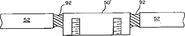
图7显示了关于导热基片50′的另一实施例。此基片50′省掉了基片50中的突出部分62。此替代方案的基片50′通过绝热固定材料92,沿其侧面68固定在PC板52上。这样,固定材料92在通孔60中,全部或部分填充了空气间隙80。此种安装方法也作为图5和图6中基片50的替代的或者附加的安装方法。一种示范材料92为聚胺酯合成橡胶,如密执安州East Lansing的Ciba-Geigy公司Formulated Materials Group的RP 6403-1树脂及固化剂(REN:C:O-THANETM)。
图8显示了关于导热基片50″的另一个实施例。此基片50″包括在每个角的、代替基片50突出部分62的安装翼片94。基片50″与基片50或50′相似,用焊接安装或粘贴方法安装。用焊接方法时,把焊料74涂在通孔60的各个与安装翼片94相应的角上。基片50″与焊料接触,加热基片使焊料融化并使基片50″在安装翼片94处附着在PC板上。
根据本发明的最佳实施例,利用热安装带65安装IC42,以通过粘合材料提供IC42与基片50间的平面紧密热接触。另一方法是,利用常规的表面安装或其他技术将IC42安装在基片50上。基片50有上表面64,其面积至少与IC42的底面82的一样大。所述基片上表面64面积最好比IC下表面82的面积大,较大的面积更有利于从IC42导出热量。
在一个实施例中,散热片90安装在基片50/50′/50上。所述基片上车有供装配螺丝96用的螺孔,螺丝96将散热片固定在基片上。该散热片比基片延伸面积更大。在一些实施例中,散热片90也固定在PC板52的下表面70上。其结果是许多通过基片50导向下表面70的热量被散热片90吸收,而不是流向IC42附近的其他IC。在另一个实施例中,散热片安装在PC板52上,并保持与基片50的物理接触。
基片50/50′/50″成为将热量从IC42导向散热片90的有效的热传导途径。由于IC42安装在基片上,IC42与PC板52间没有直接的热传导。因为基片与PC板上的通孔60的侧壁没有物理接触,基本没有热量通过所述基片导入PC板52。由于散热片90保持与PC板下表面70热接触,所以,所述PC板由基片通过传导吸收的唯一热量,是与散热片90的热接触。借助于把IC42安装在基片上,消除了通常由IC到PC板的热传导途径。而由于在基片50与PC板52的54,58各层间形成了空气间隙,避免了其他潜在的热传导途径。
本发明的一个优点在于:诸如高速微处理器等的特定集成电路与相邻电路间的热传导减少了。另一优点是建立起特定集成电路与散热片间的高效热传导途径。再一优点是建立起特定集成电路与所述基片间的有效的热接触。还有一个优点是导热基片与PC板间热传导通道不畅。
本发明的另一优点还在于基片50/50′/50″可采用简单的焊接(如基片50/50″)或粘接工艺直接安装在PCB(基片50/50′/50)上。与图4所示用螺丝固定在导热结构上相比,焊接和粘合工艺防止了相对PC板的运动。这也防止了聚酰胺构架18的内外引线20,22承受运动压力。不需要其他保持IC在适当位置的紧固装置。
虽然已介绍和描述了本发明的最佳实施例,但是,人们也可以采用各种替代方案、改型和等同物。因此,不应把以前的描述看作对本发明范围的限制,本发明的范围由所附的权利要求书限定。
Claims (7)
1.一种在集成电路(42)与散热片(90)之间建立热传导途径的方法,该方法包括:
把所述集成电路固定成与基片上的第一表面(64)热接触的状态,所述集成电路有底面(82),所述基片的第一表面面积至少与所述集成电路的底面面积一样大;以及
把所述散热片(90)安装成与所述基片热接触,而不在散热片与PC板间形成直接热接触;
其特征在于还包括以下步骤:
把导热基片(50)安装到PC板(52)的通孔(60)中,该基片被安装到所述PC板(52)的靠近通孔(60)的第一表面(70)上,以形成由通孔向外扩展的有第一长度的接触区,所述第一长度小于PC板的厚度,以便将所述基片与PC板间的热流通减至最小。
2.权利要求1的方法,其特征在于安装步骤包括:
在所述PC板的通孔中插入所述基片,所插入的基片具有沿PC板的外表面、在通孔附近延伸的第二表面(62),其中,焊料(74)涂在所述基片第二表面和所述PC板外表面之间;而且
加热所述基片以液化焊料从而把基片附着在PC板上。
3.权利要求1的方法,其特征在于安装步骤包括:
在所述PC板的通孔中插入基片;以及
将基片粘合到所述通孔壁上。
4.权利要求1的方法,其特征在于,所述基片与PC板通孔壁间有空气间隙(80)。
5.从集成电路(42)导出热量的装置,所述集成电路有底面(82),所述装置包括:
PC板(52),该PC板的第一区上有第一厚度的通孔(60),所述第一区是该PC板上有通孔的区域;以及
导热基片(50),安装在所述通孔内,该导热基片具有第一表面(64),其面积至少和集成电路底面面积一样大;
其特征在于:
所述集成电路固定成其底面与导热基片第一表面热接触,并且其中导热基片安装在所述PC板的靠近通孔(60)的第一表面(70)上,以形成由通孔向外扩展的有第一长度的接触区,所述第一长度小于PC板的厚度,以便将所述基片与PC板间的热流通减至最小。
6.权利要求5的装置,其特征在于,所述导热基片(50’)第一表面(64)面积小于所述第一区(60),其中导热基片有与第一表面相对的、面积小于第一区的第二表面(66),而其中基片通过隔热粘合剂(92)与PC板间隔开来。
7.权利要求5的装置,其特征在于,还包括可拆卸地安装成与所述基片热接触的散热片(90),而不形成散热片与所述PC板间的直接热接触。
Applications Claiming Priority (3)
| Application Number | Priority Date | Filing Date | Title |
|---|---|---|---|
| US728,394 | 1985-04-29 | ||
| US08/728,394 US5825625A (en) | 1996-05-20 | 1996-10-09 | Heat conductive substrate mounted in PC board for transferring heat from IC to heat sink |
| US728394 | 1996-10-09 |
Publications (2)
| Publication Number | Publication Date |
|---|---|
| CN1180856A CN1180856A (zh) | 1998-05-06 |
| CN1120399C true CN1120399C (zh) | 2003-09-03 |
Family
ID=24926677
Family Applications (1)
| Application Number | Title | Priority Date | Filing Date |
|---|---|---|---|
| CN97121122A Expired - Fee Related CN1120399C (zh) | 1996-10-09 | 1997-09-30 | 在集成电路与散热片间建立热传导的方法及其装置 |
Country Status (7)
| Country | Link |
|---|---|
| US (1) | US5825625A (zh) |
| EP (1) | EP0836227A3 (zh) |
| JP (1) | JPH10125832A (zh) |
| KR (1) | KR100486983B1 (zh) |
| CN (1) | CN1120399C (zh) |
| SG (1) | SG72730A1 (zh) |
| TW (1) | TW355913B (zh) |
Families Citing this family (52)
| Publication number | Priority date | Publication date | Assignee | Title |
|---|---|---|---|---|
| JP2844558B2 (ja) * | 1995-06-29 | 1999-01-06 | 信越ポリマー株式会社 | チップ状半導体素子装着用の配線回路基板およびその製造方法 |
| US5960535A (en) * | 1997-10-28 | 1999-10-05 | Hewlett-Packard Company | Heat conductive substrate press-mounted in PC board hole for transferring heat from IC to heat sink |
| US6147869A (en) * | 1997-11-24 | 2000-11-14 | International Rectifier Corp. | Adaptable planar module |
| US6292374B1 (en) * | 1998-05-29 | 2001-09-18 | Lucent Technologies, Inc. | Assembly having a back plate with inserts |
| US6067231A (en) * | 1998-11-10 | 2000-05-23 | Acer Peripherals, Inc. | Heat-dissipating structure for an electrical device |
| US6352203B1 (en) * | 1999-03-17 | 2002-03-05 | Compaq Information Technologies Group, L.P. | Automated semiconductor identification system |
| DE19949429C2 (de) * | 1999-10-13 | 2003-10-09 | Conti Temic Microelectronic | Verfahren zur Bearbeitung einer durchkontaktierten Leiterplatte |
| US6570764B2 (en) * | 1999-12-29 | 2003-05-27 | Intel Corporation | Low thermal resistance interface for attachment of thermal materials to a processor die |
| US6560108B2 (en) * | 2000-02-16 | 2003-05-06 | Hughes Electronics Corporation | Chip scale packaging on CTE matched printed wiring boards |
| US6295200B1 (en) * | 2000-02-23 | 2001-09-25 | Motorola, Inc. | Carrier assembly and method |
| KR100332314B1 (ko) * | 2000-06-24 | 2002-04-12 | 서성기 | 박막증착용 반응용기 |
| JP3532871B2 (ja) | 2001-02-28 | 2004-05-31 | 株式会社東芝 | 冷却装置およびこの冷却装置を有する電子機器 |
| US6580611B1 (en) * | 2001-12-21 | 2003-06-17 | Intel Corporation | Dual-sided heat removal system |
| US6762939B2 (en) * | 2002-02-20 | 2004-07-13 | Intel Corporation | Thermal solution for a mezzanine card |
| FR2839607B1 (fr) * | 2002-05-07 | 2004-09-10 | Univ Angers | Assemblage de composants de puissance sur un circuit imprime ainsi qu'un procede d'obtention d'un tel assemblage |
| US6625028B1 (en) * | 2002-06-20 | 2003-09-23 | Agilent Technologies, Inc. | Heat sink apparatus that provides electrical isolation for integrally shielded circuit |
| JP2004140267A (ja) | 2002-10-18 | 2004-05-13 | Semiconductor Energy Lab Co Ltd | 半導体装置およびその作製方法 |
| US7229636B1 (en) | 2003-03-04 | 2007-06-12 | Nastech Pharmaceutical Company Inc. | Cyanocobalamin low viscosity aqueous formulations for intranasal delivery |
| US7404489B1 (en) | 2003-03-04 | 2008-07-29 | Qol Medical, Llc | Cyanocobalamin low viscosity aqueous formulations for intranasal delivery |
| US20040184236A1 (en) * | 2003-03-20 | 2004-09-23 | Kuang-Yao Lee | Central processing unit (CPU) heat sink module |
| US20040188811A1 (en) * | 2003-03-24 | 2004-09-30 | Intel Corporation | Circuit package apparatus, systems, and methods |
| US20040218363A1 (en) * | 2003-04-30 | 2004-11-04 | Wong Marvin Glenn | Application specific heat-dissipating apparatus that provides electrical isolation for components |
| CN100391017C (zh) * | 2003-05-26 | 2008-05-28 | 松下电工株式会社 | 发光器件 |
| TWI253765B (en) * | 2003-05-26 | 2006-04-21 | Matsushita Electric Works Ltd | Light-emitting device |
| US6928380B2 (en) * | 2003-10-30 | 2005-08-09 | International Business Machines Corporation | Thermal measurements of electronic devices during operation |
| GB0413420D0 (en) * | 2004-06-15 | 2004-07-21 | Radstone Technology Plc | Heat management in printed wiring boards |
| CN101066008A (zh) * | 2004-11-30 | 2007-10-31 | Lm爱立信电话有限公司 | 改进了散热的印刷电路板组件 |
| DE102005013762C5 (de) | 2005-03-22 | 2012-12-20 | Sew-Eurodrive Gmbh & Co. Kg | Elektronisches Gerät und Verfahren zur Bestimmung der Temperatur eines Leistungshalbleiters |
| JP4711715B2 (ja) * | 2005-03-30 | 2011-06-29 | 株式会社東芝 | 半導体発光装置及び半導体発光ユニット |
| JP2009504767A (ja) | 2005-08-17 | 2009-02-05 | フレミング・アンド・カンパニー・ファーマシューティカルズ | ビタミンb12鼻用スプレーおよび使用方法 |
| US20070076377A1 (en) * | 2005-10-03 | 2007-04-05 | Matteo Gravina | Bi-Polar Thermal Managment |
| DE102005049872B4 (de) * | 2005-10-18 | 2010-09-23 | Continental Automotive Gmbh | IC-Bauelement mit Kühlanordnung |
| US7355854B2 (en) * | 2006-06-07 | 2008-04-08 | Harris Corporation | Apparatus for improved grounding of flange mount field effect transistors to printed wiring boards |
| FR2902277B1 (fr) * | 2006-06-13 | 2008-09-05 | Valeo Electronique Sys Liaison | Support pour composant electrique et dispositif electrique comprenant le support et le composant |
| JP2008060430A (ja) * | 2006-08-31 | 2008-03-13 | Daikin Ind Ltd | 電力変換装置 |
| TWI324669B (en) * | 2007-03-15 | 2010-05-11 | Ind Tech Res Inst | Light modules |
| US20080258167A1 (en) * | 2007-04-23 | 2008-10-23 | Liu Ming-Dah | Package structure for light-emitting elements |
| DE102007037297A1 (de) * | 2007-08-07 | 2009-02-19 | Continental Automotive Gmbh | Schaltungsträgeraufbau mit verbesserter Wärmeableitung |
| JP5324773B2 (ja) * | 2007-11-06 | 2013-10-23 | インターナショナル・ビジネス・マシーンズ・コーポレーション | 回路モジュールとその製造方法 |
| US7706144B2 (en) * | 2007-12-17 | 2010-04-27 | Lynch Thomas W | Heat dissipation system and related method |
| TWI380419B (en) * | 2008-01-16 | 2012-12-21 | Raydium Semiconductor Corp | Integrated circuit package and the method for fabricating thereof |
| US7724528B2 (en) * | 2008-07-11 | 2010-05-25 | Cisco Technology, Inc. | Thermal dissipation heat slug sandwich |
| CN102549741B (zh) * | 2010-08-20 | 2014-11-05 | 松下电器产业株式会社 | 半导体装置及其制造方法 |
| EP2442627A1 (de) * | 2010-10-15 | 2012-04-18 | Odelo GmbH | Kraftfahrzeugleuchte |
| JP2013038119A (ja) * | 2011-08-04 | 2013-02-21 | Mitsubishi Electric Corp | モジュールの取付け構造 |
| CN102612302A (zh) * | 2012-03-13 | 2012-07-25 | 华为技术有限公司 | 光模块散热装置及通信设备 |
| US9420722B2 (en) * | 2012-12-06 | 2016-08-16 | Gerald Ho Kim | Composite heat sink device for cooling of multiple heat sources in close proximity |
| US9575523B2 (en) | 2015-01-22 | 2017-02-21 | Microsoft Technology Licensing, Llc | Device sandwich structured composite housing |
| US20170089648A1 (en) * | 2015-09-24 | 2017-03-30 | Jones Tech (USA), Inc. | Adhesive-thermal gasket |
| US10504813B2 (en) * | 2016-09-30 | 2019-12-10 | Astec International Limited | Heat sink assemblies for surface mounted devices |
| US11646240B2 (en) * | 2021-02-03 | 2023-05-09 | Nvidia Corporation | Through-hole mounted semiconductor assemblies |
| KR20230112404A (ko) | 2022-01-20 | 2023-07-27 | 오일성 | 회전형 버블파이프를 갖는 초음파 세척기 |
Family Cites Families (23)
| Publication number | Priority date | Publication date | Assignee | Title |
|---|---|---|---|---|
| US4420767A (en) * | 1978-11-09 | 1983-12-13 | Zilog, Inc. | Thermally balanced leadless microelectronic circuit chip carrier |
| EP0103068B1 (de) * | 1982-09-09 | 1989-01-04 | Siemens Aktiengesellschaft | Einrichtung zum Kühlen einer Mehrzahl von zu Flachbaugruppen zusammengefassten integrierten Bausteinen |
| US4602314A (en) * | 1983-10-14 | 1986-07-22 | Intel Corporation | Heat conduction mechanism for semiconductor devices |
| IT1213139B (it) * | 1984-02-17 | 1989-12-14 | Ates Componenti Elettron | Componente elettronico integrato di tipo "single-in-line" eprocedimento per la sua fabbricazione. |
| US4750089A (en) * | 1985-11-22 | 1988-06-07 | Texas Instruments Incorporated | Circuit board with a chip carrier and mounting structure connected to the chip carrier |
| US4731693A (en) * | 1986-09-29 | 1988-03-15 | Tektronix, Inc. | Connection apparatus for integrated circuit |
| JPS63136655A (ja) * | 1986-11-28 | 1988-06-08 | Nec Corp | チツプキヤリア |
| JP2590521B2 (ja) * | 1988-03-29 | 1997-03-12 | 日本電気株式会社 | チップキャリア |
| US4849856A (en) * | 1988-07-13 | 1989-07-18 | International Business Machines Corp. | Electronic package with improved heat sink |
| JPH0279451A (ja) * | 1988-09-14 | 1990-03-20 | Hitachi Ltd | 半導体装置およびその製造方法 |
| US5095404A (en) * | 1990-02-26 | 1992-03-10 | Data General Corporation | Arrangement for mounting and cooling high density tab IC chips |
| JP2745786B2 (ja) * | 1990-06-15 | 1998-04-28 | 松下電器産業株式会社 | Tab半導体装置 |
| JP2853288B2 (ja) * | 1990-07-19 | 1999-02-03 | 日本電気株式会社 | 半導体装置 |
| IT1250405B (it) * | 1991-01-31 | 1995-04-07 | Sgs Thomson Microelectronics | Piastrina metallica di dissipazione del calore di un dispositivo a semiconduttore di potenza incapsulato in resina fornita di rilievi per la saldatura dei fili di massa |
| JPH0582685A (ja) * | 1991-09-24 | 1993-04-02 | Mitsubishi Electric Corp | 混成集積部品の放熱部および端子部用構造体とその構造体を用いた混成集積部品の製造方法 |
| US5263245A (en) * | 1992-01-27 | 1993-11-23 | International Business Machines Corporation | Method of making an electronic package with enhanced heat sinking |
| JPH05315467A (ja) * | 1992-05-06 | 1993-11-26 | Mitsubishi Electric Corp | 混成集積回路装置 |
| US5278724A (en) * | 1992-07-06 | 1994-01-11 | International Business Machines Corporation | Electronic package and method of making same |
| DE4232575A1 (de) * | 1992-09-29 | 1994-03-31 | Bosch Gmbh Robert | Anordnung mit einer Leiterplatte, mindestens einem Leistungsbauelement und einem Kühlkörper |
| US5410451A (en) * | 1993-12-20 | 1995-04-25 | Lsi Logic Corporation | Location and standoff pins for chip on tape |
| US5578869A (en) * | 1994-03-29 | 1996-11-26 | Olin Corporation | Components for housing an integrated circuit device |
| JP3485958B2 (ja) * | 1994-04-08 | 2004-01-13 | 株式会社東芝 | 記録媒体再生装置及び記録媒体再生方法 |
| US5617294A (en) * | 1995-09-29 | 1997-04-01 | Intel Corporation | Apparatus for removing heat from an integrated circuit package that is attached to a printed circuit board |
-
1996
- 1996-10-09 US US08/728,394 patent/US5825625A/en not_active Expired - Lifetime
-
1997
- 1997-03-04 SG SG1997000645A patent/SG72730A1/en unknown
- 1997-03-04 TW TW086102586A patent/TW355913B/zh active
- 1997-09-15 EP EP97307122A patent/EP0836227A3/en not_active Ceased
- 1997-09-30 CN CN97121122A patent/CN1120399C/zh not_active Expired - Fee Related
- 1997-10-02 JP JP9269459A patent/JPH10125832A/ja active Pending
- 1997-10-08 KR KR1019970051556A patent/KR100486983B1/ko not_active IP Right Cessation
Also Published As
| Publication number | Publication date |
|---|---|
| CN1180856A (zh) | 1998-05-06 |
| KR100486983B1 (ko) | 2005-06-16 |
| JPH10125832A (ja) | 1998-05-15 |
| KR19980032644A (ko) | 1998-07-25 |
| US5825625A (en) | 1998-10-20 |
| TW355913B (en) | 1999-04-11 |
| SG72730A1 (en) | 2000-05-23 |
| EP0836227A2 (en) | 1998-04-15 |
| EP0836227A3 (en) | 1999-03-10 |
Similar Documents
| Publication | Publication Date | Title |
|---|---|---|
| CN1120399C (zh) | 在集成电路与散热片间建立热传导的方法及其装置 | |
| CN1155082C (zh) | 从集成电路散热的方法和装置 | |
| CN101213892B (zh) | 发光二极管封装件及其制造方法 | |
| CN1107978C (zh) | 带有导热支持元件的电子封装件 | |
| US8100567B2 (en) | Light-emitting devices and related systems | |
| US5767576A (en) | Semiconductor module with snap line | |
| US20080099777A1 (en) | Light-emitting devices and related systems | |
| JPH0677679A (ja) | 回路基板に電気素子を取り付ける方法及びその装置 | |
| CN1830085A (zh) | 散热电子装置 | |
| JPH11346480A (ja) | インバータ装置 | |
| CN101388368A (zh) | 半导体模块装置及其制造方法以及显示装置、显示面板 | |
| KR20090093963A (ko) | 발광 장치, 표시 장치, 및 고체 발광 소자 기판 | |
| KR100510383B1 (ko) | 제어기 | |
| CN101472449A (zh) | 散热器与电路的结合结构及结合方法 | |
| JPH08148839A (ja) | 混成集積回路装置 | |
| JPH06309532A (ja) | Icカード | |
| US5804873A (en) | Heatsink for surface mount device for circuit board mounting | |
| CN101180498A (zh) | Led照明模块组件 | |
| JP3039488B2 (ja) | 半導体装置 | |
| CN113727515A (zh) | 一种金属覆铜板 | |
| JPH1093250A (ja) | プリント配線板の放熱構造 | |
| CN219087385U (zh) | 一种多层软性线路板结构 | |
| CN212033007U (zh) | 一种带有散热结构的电子设备用芯片 | |
| JPH04284655A (ja) | 半導体集積回路装置 | |
| CA1203640A (en) | Apparatus for cooling integrated circuit chips |
Legal Events
| Date | Code | Title | Description |
|---|---|---|---|
| C06 | Publication | ||
| PB01 | Publication | ||
| C10 | Entry into substantive examination | ||
| SE01 | Entry into force of request for substantive examination | ||
| C14 | Grant of patent or utility model | ||
| GR01 | Patent grant | ||
| C19 | Lapse of patent right due to non-payment of the annual fee | ||
| CF01 | Termination of patent right due to non-payment of annual fee |