CN106952877B - 半导体装置 - Google Patents
半导体装置 Download PDFInfo
- Publication number
- CN106952877B CN106952877B CN201611055874.2A CN201611055874A CN106952877B CN 106952877 B CN106952877 B CN 106952877B CN 201611055874 A CN201611055874 A CN 201611055874A CN 106952877 B CN106952877 B CN 106952877B
- Authority
- CN
- China
- Prior art keywords
- semiconductor element
- lead terminal
- semiconductor device
- lead
- bonded
- Prior art date
- Legal status (The legal status is an assumption and is not a legal conclusion. Google has not performed a legal analysis and makes no representation as to the accuracy of the status listed.)
- Active
Links
Images


Classifications
-
- H—ELECTRICITY
- H01—ELECTRIC ELEMENTS
- H01L—SEMICONDUCTOR DEVICES NOT COVERED BY CLASS H10
- H01L23/00—Details of semiconductor or other solid state devices
- H01L23/28—Encapsulations, e.g. encapsulating layers, coatings, e.g. for protection
- H01L23/29—Encapsulations, e.g. encapsulating layers, coatings, e.g. for protection characterised by the material, e.g. carbon
-
- H—ELECTRICITY
- H01—ELECTRIC ELEMENTS
- H01L—SEMICONDUCTOR DEVICES NOT COVERED BY CLASS H10
- H01L24/00—Arrangements for connecting or disconnecting semiconductor or solid-state bodies; Methods or apparatus related thereto
- H01L24/01—Means for bonding being attached to, or being formed on, the surface to be connected, e.g. chip-to-package, die-attach, "first-level" interconnects; Manufacturing methods related thereto
- H01L24/42—Wire connectors; Manufacturing methods related thereto
- H01L24/47—Structure, shape, material or disposition of the wire connectors after the connecting process
-
- H—ELECTRICITY
- H01—ELECTRIC ELEMENTS
- H01L—SEMICONDUCTOR DEVICES NOT COVERED BY CLASS H10
- H01L23/00—Details of semiconductor or other solid state devices
- H01L23/562—Protection against mechanical damage
-
- H—ELECTRICITY
- H01—ELECTRIC ELEMENTS
- H01L—SEMICONDUCTOR DEVICES NOT COVERED BY CLASS H10
- H01L23/00—Details of semiconductor or other solid state devices
-
- H—ELECTRICITY
- H01—ELECTRIC ELEMENTS
- H01L—SEMICONDUCTOR DEVICES NOT COVERED BY CLASS H10
- H01L23/00—Details of semiconductor or other solid state devices
- H01L23/28—Encapsulations, e.g. encapsulating layers, coatings, e.g. for protection
- H01L23/29—Encapsulations, e.g. encapsulating layers, coatings, e.g. for protection characterised by the material, e.g. carbon
- H01L23/293—Organic, e.g. plastic
-
- H—ELECTRICITY
- H01—ELECTRIC ELEMENTS
- H01L—SEMICONDUCTOR DEVICES NOT COVERED BY CLASS H10
- H01L23/00—Details of semiconductor or other solid state devices
- H01L23/28—Encapsulations, e.g. encapsulating layers, coatings, e.g. for protection
- H01L23/31—Encapsulations, e.g. encapsulating layers, coatings, e.g. for protection characterised by the arrangement or shape
- H01L23/3107—Encapsulations, e.g. encapsulating layers, coatings, e.g. for protection characterised by the arrangement or shape the device being completely enclosed
- H01L23/3121—Encapsulations, e.g. encapsulating layers, coatings, e.g. for protection characterised by the arrangement or shape the device being completely enclosed a substrate forming part of the encapsulation
-
- H—ELECTRICITY
- H01—ELECTRIC ELEMENTS
- H01L—SEMICONDUCTOR DEVICES NOT COVERED BY CLASS H10
- H01L23/00—Details of semiconductor or other solid state devices
- H01L23/28—Encapsulations, e.g. encapsulating layers, coatings, e.g. for protection
- H01L23/31—Encapsulations, e.g. encapsulating layers, coatings, e.g. for protection characterised by the arrangement or shape
- H01L23/3107—Encapsulations, e.g. encapsulating layers, coatings, e.g. for protection characterised by the arrangement or shape the device being completely enclosed
- H01L23/3135—Double encapsulation or coating and encapsulation
-
- H—ELECTRICITY
- H01—ELECTRIC ELEMENTS
- H01L—SEMICONDUCTOR DEVICES NOT COVERED BY CLASS H10
- H01L23/00—Details of semiconductor or other solid state devices
- H01L23/28—Encapsulations, e.g. encapsulating layers, coatings, e.g. for protection
- H01L23/31—Encapsulations, e.g. encapsulating layers, coatings, e.g. for protection characterised by the arrangement or shape
- H01L23/3157—Partial encapsulation or coating
- H01L23/3185—Partial encapsulation or coating the coating covering also the sidewalls of the semiconductor body
-
- H—ELECTRICITY
- H01—ELECTRIC ELEMENTS
- H01L—SEMICONDUCTOR DEVICES NOT COVERED BY CLASS H10
- H01L23/00—Details of semiconductor or other solid state devices
- H01L23/48—Arrangements for conducting electric current to or from the solid state body in operation, e.g. leads, terminal arrangements ; Selection of materials therefor
- H01L23/488—Arrangements for conducting electric current to or from the solid state body in operation, e.g. leads, terminal arrangements ; Selection of materials therefor consisting of soldered or bonded constructions
- H01L23/495—Lead-frames or other flat leads
- H01L23/49517—Additional leads
- H01L23/4952—Additional leads the additional leads being a bump or a wire
-
- H—ELECTRICITY
- H01—ELECTRIC ELEMENTS
- H01L—SEMICONDUCTOR DEVICES NOT COVERED BY CLASS H10
- H01L23/00—Details of semiconductor or other solid state devices
- H01L23/48—Arrangements for conducting electric current to or from the solid state body in operation, e.g. leads, terminal arrangements ; Selection of materials therefor
- H01L23/488—Arrangements for conducting electric current to or from the solid state body in operation, e.g. leads, terminal arrangements ; Selection of materials therefor consisting of soldered or bonded constructions
- H01L23/495—Lead-frames or other flat leads
- H01L23/49541—Geometry of the lead-frame
- H01L23/49548—Cross section geometry
- H01L23/49551—Cross section geometry characterised by bent parts
-
- H—ELECTRICITY
- H01—ELECTRIC ELEMENTS
- H01L—SEMICONDUCTOR DEVICES NOT COVERED BY CLASS H10
- H01L23/00—Details of semiconductor or other solid state devices
- H01L23/48—Arrangements for conducting electric current to or from the solid state body in operation, e.g. leads, terminal arrangements ; Selection of materials therefor
- H01L23/488—Arrangements for conducting electric current to or from the solid state body in operation, e.g. leads, terminal arrangements ; Selection of materials therefor consisting of soldered or bonded constructions
- H01L23/495—Lead-frames or other flat leads
- H01L23/49575—Assemblies of semiconductor devices on lead frames
-
- H—ELECTRICITY
- H01—ELECTRIC ELEMENTS
- H01L—SEMICONDUCTOR DEVICES NOT COVERED BY CLASS H10
- H01L23/00—Details of semiconductor or other solid state devices
- H01L23/48—Arrangements for conducting electric current to or from the solid state body in operation, e.g. leads, terminal arrangements ; Selection of materials therefor
- H01L23/488—Arrangements for conducting electric current to or from the solid state body in operation, e.g. leads, terminal arrangements ; Selection of materials therefor consisting of soldered or bonded constructions
- H01L23/498—Leads, i.e. metallisations or lead-frames on insulating substrates, e.g. chip carriers
- H01L23/49838—Geometry or layout
-
- H—ELECTRICITY
- H01—ELECTRIC ELEMENTS
- H01L—SEMICONDUCTOR DEVICES NOT COVERED BY CLASS H10
- H01L24/00—Arrangements for connecting or disconnecting semiconductor or solid-state bodies; Methods or apparatus related thereto
- H01L24/01—Means for bonding being attached to, or being formed on, the surface to be connected, e.g. chip-to-package, die-attach, "first-level" interconnects; Manufacturing methods related thereto
- H01L24/34—Strap connectors, e.g. copper straps for grounding power devices; Manufacturing methods related thereto
- H01L24/36—Structure, shape, material or disposition of the strap connectors prior to the connecting process
- H01L24/37—Structure, shape, material or disposition of the strap connectors prior to the connecting process of an individual strap connector
-
- H—ELECTRICITY
- H01—ELECTRIC ELEMENTS
- H01L—SEMICONDUCTOR DEVICES NOT COVERED BY CLASS H10
- H01L24/00—Arrangements for connecting or disconnecting semiconductor or solid-state bodies; Methods or apparatus related thereto
- H01L24/01—Means for bonding being attached to, or being formed on, the surface to be connected, e.g. chip-to-package, die-attach, "first-level" interconnects; Manufacturing methods related thereto
- H01L24/34—Strap connectors, e.g. copper straps for grounding power devices; Manufacturing methods related thereto
- H01L24/39—Structure, shape, material or disposition of the strap connectors after the connecting process
- H01L24/40—Structure, shape, material or disposition of the strap connectors after the connecting process of an individual strap connector
-
- H—ELECTRICITY
- H01—ELECTRIC ELEMENTS
- H01L—SEMICONDUCTOR DEVICES NOT COVERED BY CLASS H10
- H01L25/00—Assemblies consisting of a plurality of individual semiconductor or other solid state devices ; Multistep manufacturing processes thereof
- H01L25/03—Assemblies consisting of a plurality of individual semiconductor or other solid state devices ; Multistep manufacturing processes thereof all the devices being of a type provided for in the same subgroup of groups H01L27/00 - H01L33/00, or in a single subclass of H10K, H10N, e.g. assemblies of rectifier diodes
- H01L25/04—Assemblies consisting of a plurality of individual semiconductor or other solid state devices ; Multistep manufacturing processes thereof all the devices being of a type provided for in the same subgroup of groups H01L27/00 - H01L33/00, or in a single subclass of H10K, H10N, e.g. assemblies of rectifier diodes the devices not having separate containers
- H01L25/07—Assemblies consisting of a plurality of individual semiconductor or other solid state devices ; Multistep manufacturing processes thereof all the devices being of a type provided for in the same subgroup of groups H01L27/00 - H01L33/00, or in a single subclass of H10K, H10N, e.g. assemblies of rectifier diodes the devices not having separate containers the devices being of a type provided for in group H01L29/00
- H01L25/072—Assemblies consisting of a plurality of individual semiconductor or other solid state devices ; Multistep manufacturing processes thereof all the devices being of a type provided for in the same subgroup of groups H01L27/00 - H01L33/00, or in a single subclass of H10K, H10N, e.g. assemblies of rectifier diodes the devices not having separate containers the devices being of a type provided for in group H01L29/00 the devices being arranged next to each other
-
- H—ELECTRICITY
- H01—ELECTRIC ELEMENTS
- H01L—SEMICONDUCTOR DEVICES NOT COVERED BY CLASS H10
- H01L25/00—Assemblies consisting of a plurality of individual semiconductor or other solid state devices ; Multistep manufacturing processes thereof
- H01L25/18—Assemblies consisting of a plurality of individual semiconductor or other solid state devices ; Multistep manufacturing processes thereof the devices being of types provided for in two or more different subgroups of the same main group of groups H01L27/00 - H01L33/00, or in a single subclass of H10K, H10N
-
- H—ELECTRICITY
- H01—ELECTRIC ELEMENTS
- H01L—SEMICONDUCTOR DEVICES NOT COVERED BY CLASS H10
- H01L2224/00—Indexing scheme for arrangements for connecting or disconnecting semiconductor or solid-state bodies and methods related thereto as covered by H01L24/00
- H01L2224/01—Means for bonding being attached to, or being formed on, the surface to be connected, e.g. chip-to-package, die-attach, "first-level" interconnects; Manufacturing methods related thereto
- H01L2224/02—Bonding areas; Manufacturing methods related thereto
- H01L2224/04—Structure, shape, material or disposition of the bonding areas prior to the connecting process
- H01L2224/05—Structure, shape, material or disposition of the bonding areas prior to the connecting process of an individual bonding area
- H01L2224/0554—External layer
- H01L2224/0555—Shape
- H01L2224/05552—Shape in top view
- H01L2224/05554—Shape in top view being square
-
- H—ELECTRICITY
- H01—ELECTRIC ELEMENTS
- H01L—SEMICONDUCTOR DEVICES NOT COVERED BY CLASS H10
- H01L2224/00—Indexing scheme for arrangements for connecting or disconnecting semiconductor or solid-state bodies and methods related thereto as covered by H01L24/00
- H01L2224/01—Means for bonding being attached to, or being formed on, the surface to be connected, e.g. chip-to-package, die-attach, "first-level" interconnects; Manufacturing methods related thereto
- H01L2224/02—Bonding areas; Manufacturing methods related thereto
- H01L2224/04—Structure, shape, material or disposition of the bonding areas prior to the connecting process
- H01L2224/06—Structure, shape, material or disposition of the bonding areas prior to the connecting process of a plurality of bonding areas
- H01L2224/0601—Structure
- H01L2224/0603—Bonding areas having different sizes, e.g. different heights or widths
-
- H—ELECTRICITY
- H01—ELECTRIC ELEMENTS
- H01L—SEMICONDUCTOR DEVICES NOT COVERED BY CLASS H10
- H01L2224/00—Indexing scheme for arrangements for connecting or disconnecting semiconductor or solid-state bodies and methods related thereto as covered by H01L24/00
- H01L2224/01—Means for bonding being attached to, or being formed on, the surface to be connected, e.g. chip-to-package, die-attach, "first-level" interconnects; Manufacturing methods related thereto
- H01L2224/34—Strap connectors, e.g. copper straps for grounding power devices; Manufacturing methods related thereto
- H01L2224/36—Structure, shape, material or disposition of the strap connectors prior to the connecting process
- H01L2224/37—Structure, shape, material or disposition of the strap connectors prior to the connecting process of an individual strap connector
- H01L2224/37001—Core members of the connector
- H01L2224/37099—Material
- H01L2224/371—Material with a principal constituent of the material being a metal or a metalloid, e.g. boron [B], silicon [Si], germanium [Ge], arsenic [As], antimony [Sb], tellurium [Te] and polonium [Po], and alloys thereof
- H01L2224/37117—Material with a principal constituent of the material being a metal or a metalloid, e.g. boron [B], silicon [Si], germanium [Ge], arsenic [As], antimony [Sb], tellurium [Te] and polonium [Po], and alloys thereof the principal constituent melting at a temperature of greater than or equal to 400°C and less than 950°C
- H01L2224/37124—Aluminium [Al] as principal constituent
-
- H—ELECTRICITY
- H01—ELECTRIC ELEMENTS
- H01L—SEMICONDUCTOR DEVICES NOT COVERED BY CLASS H10
- H01L2224/00—Indexing scheme for arrangements for connecting or disconnecting semiconductor or solid-state bodies and methods related thereto as covered by H01L24/00
- H01L2224/01—Means for bonding being attached to, or being formed on, the surface to be connected, e.g. chip-to-package, die-attach, "first-level" interconnects; Manufacturing methods related thereto
- H01L2224/34—Strap connectors, e.g. copper straps for grounding power devices; Manufacturing methods related thereto
- H01L2224/36—Structure, shape, material or disposition of the strap connectors prior to the connecting process
- H01L2224/37—Structure, shape, material or disposition of the strap connectors prior to the connecting process of an individual strap connector
- H01L2224/37001—Core members of the connector
- H01L2224/37099—Material
- H01L2224/371—Material with a principal constituent of the material being a metal or a metalloid, e.g. boron [B], silicon [Si], germanium [Ge], arsenic [As], antimony [Sb], tellurium [Te] and polonium [Po], and alloys thereof
- H01L2224/37138—Material with a principal constituent of the material being a metal or a metalloid, e.g. boron [B], silicon [Si], germanium [Ge], arsenic [As], antimony [Sb], tellurium [Te] and polonium [Po], and alloys thereof the principal constituent melting at a temperature of greater than or equal to 950°C and less than 1550°C
- H01L2224/37147—Copper [Cu] as principal constituent
-
- H—ELECTRICITY
- H01—ELECTRIC ELEMENTS
- H01L—SEMICONDUCTOR DEVICES NOT COVERED BY CLASS H10
- H01L2224/00—Indexing scheme for arrangements for connecting or disconnecting semiconductor or solid-state bodies and methods related thereto as covered by H01L24/00
- H01L2224/01—Means for bonding being attached to, or being formed on, the surface to be connected, e.g. chip-to-package, die-attach, "first-level" interconnects; Manufacturing methods related thereto
- H01L2224/34—Strap connectors, e.g. copper straps for grounding power devices; Manufacturing methods related thereto
- H01L2224/36—Structure, shape, material or disposition of the strap connectors prior to the connecting process
- H01L2224/37—Structure, shape, material or disposition of the strap connectors prior to the connecting process of an individual strap connector
- H01L2224/3754—Coating
- H01L2224/37599—Material
- H01L2224/376—Material with a principal constituent of the material being a metal or a metalloid, e.g. boron [B], silicon [Si], germanium [Ge], arsenic [As], antimony [Sb], tellurium [Te] and polonium [Po], and alloys thereof
- H01L2224/37638—Material with a principal constituent of the material being a metal or a metalloid, e.g. boron [B], silicon [Si], germanium [Ge], arsenic [As], antimony [Sb], tellurium [Te] and polonium [Po], and alloys thereof the principal constituent melting at a temperature of greater than or equal to 950°C and less than 1550°C
- H01L2224/37639—Silver [Ag] as principal constituent
-
- H—ELECTRICITY
- H01—ELECTRIC ELEMENTS
- H01L—SEMICONDUCTOR DEVICES NOT COVERED BY CLASS H10
- H01L2224/00—Indexing scheme for arrangements for connecting or disconnecting semiconductor or solid-state bodies and methods related thereto as covered by H01L24/00
- H01L2224/01—Means for bonding being attached to, or being formed on, the surface to be connected, e.g. chip-to-package, die-attach, "first-level" interconnects; Manufacturing methods related thereto
- H01L2224/34—Strap connectors, e.g. copper straps for grounding power devices; Manufacturing methods related thereto
- H01L2224/36—Structure, shape, material or disposition of the strap connectors prior to the connecting process
- H01L2224/37—Structure, shape, material or disposition of the strap connectors prior to the connecting process of an individual strap connector
- H01L2224/3754—Coating
- H01L2224/37599—Material
- H01L2224/376—Material with a principal constituent of the material being a metal or a metalloid, e.g. boron [B], silicon [Si], germanium [Ge], arsenic [As], antimony [Sb], tellurium [Te] and polonium [Po], and alloys thereof
- H01L2224/37638—Material with a principal constituent of the material being a metal or a metalloid, e.g. boron [B], silicon [Si], germanium [Ge], arsenic [As], antimony [Sb], tellurium [Te] and polonium [Po], and alloys thereof the principal constituent melting at a temperature of greater than or equal to 950°C and less than 1550°C
- H01L2224/37644—Gold [Au] as principal constituent
-
- H—ELECTRICITY
- H01—ELECTRIC ELEMENTS
- H01L—SEMICONDUCTOR DEVICES NOT COVERED BY CLASS H10
- H01L2224/00—Indexing scheme for arrangements for connecting or disconnecting semiconductor or solid-state bodies and methods related thereto as covered by H01L24/00
- H01L2224/01—Means for bonding being attached to, or being formed on, the surface to be connected, e.g. chip-to-package, die-attach, "first-level" interconnects; Manufacturing methods related thereto
- H01L2224/34—Strap connectors, e.g. copper straps for grounding power devices; Manufacturing methods related thereto
- H01L2224/36—Structure, shape, material or disposition of the strap connectors prior to the connecting process
- H01L2224/37—Structure, shape, material or disposition of the strap connectors prior to the connecting process of an individual strap connector
- H01L2224/3754—Coating
- H01L2224/37599—Material
- H01L2224/376—Material with a principal constituent of the material being a metal or a metalloid, e.g. boron [B], silicon [Si], germanium [Ge], arsenic [As], antimony [Sb], tellurium [Te] and polonium [Po], and alloys thereof
- H01L2224/37638—Material with a principal constituent of the material being a metal or a metalloid, e.g. boron [B], silicon [Si], germanium [Ge], arsenic [As], antimony [Sb], tellurium [Te] and polonium [Po], and alloys thereof the principal constituent melting at a temperature of greater than or equal to 950°C and less than 1550°C
- H01L2224/37655—Nickel [Ni] as principal constituent
-
- H—ELECTRICITY
- H01—ELECTRIC ELEMENTS
- H01L—SEMICONDUCTOR DEVICES NOT COVERED BY CLASS H10
- H01L2224/00—Indexing scheme for arrangements for connecting or disconnecting semiconductor or solid-state bodies and methods related thereto as covered by H01L24/00
- H01L2224/01—Means for bonding being attached to, or being formed on, the surface to be connected, e.g. chip-to-package, die-attach, "first-level" interconnects; Manufacturing methods related thereto
- H01L2224/34—Strap connectors, e.g. copper straps for grounding power devices; Manufacturing methods related thereto
- H01L2224/39—Structure, shape, material or disposition of the strap connectors after the connecting process
- H01L2224/40—Structure, shape, material or disposition of the strap connectors after the connecting process of an individual strap connector
- H01L2224/401—Disposition
- H01L2224/40135—Connecting between different semiconductor or solid-state bodies, i.e. chip-to-chip
- H01L2224/40137—Connecting between different semiconductor or solid-state bodies, i.e. chip-to-chip the bodies being arranged next to each other, e.g. on a common substrate
-
- H—ELECTRICITY
- H01—ELECTRIC ELEMENTS
- H01L—SEMICONDUCTOR DEVICES NOT COVERED BY CLASS H10
- H01L2224/00—Indexing scheme for arrangements for connecting or disconnecting semiconductor or solid-state bodies and methods related thereto as covered by H01L24/00
- H01L2224/01—Means for bonding being attached to, or being formed on, the surface to be connected, e.g. chip-to-package, die-attach, "first-level" interconnects; Manufacturing methods related thereto
- H01L2224/42—Wire connectors; Manufacturing methods related thereto
- H01L2224/47—Structure, shape, material or disposition of the wire connectors after the connecting process
- H01L2224/48—Structure, shape, material or disposition of the wire connectors after the connecting process of an individual wire connector
- H01L2224/4805—Shape
- H01L2224/4809—Loop shape
- H01L2224/48091—Arched
-
- H—ELECTRICITY
- H01—ELECTRIC ELEMENTS
- H01L—SEMICONDUCTOR DEVICES NOT COVERED BY CLASS H10
- H01L2224/00—Indexing scheme for arrangements for connecting or disconnecting semiconductor or solid-state bodies and methods related thereto as covered by H01L24/00
- H01L2224/73—Means for bonding being of different types provided for in two or more of groups H01L2224/10, H01L2224/18, H01L2224/26, H01L2224/34, H01L2224/42, H01L2224/50, H01L2224/63, H01L2224/71
- H01L2224/732—Location after the connecting process
- H01L2224/73201—Location after the connecting process on the same surface
- H01L2224/73221—Strap and wire connectors
-
- H—ELECTRICITY
- H01—ELECTRIC ELEMENTS
- H01L—SEMICONDUCTOR DEVICES NOT COVERED BY CLASS H10
- H01L2224/00—Indexing scheme for arrangements for connecting or disconnecting semiconductor or solid-state bodies and methods related thereto as covered by H01L24/00
- H01L2224/80—Methods for connecting semiconductor or other solid state bodies using means for bonding being attached to, or being formed on, the surface to be connected
- H01L2224/83—Methods for connecting semiconductor or other solid state bodies using means for bonding being attached to, or being formed on, the surface to be connected using a layer connector
- H01L2224/838—Bonding techniques
- H01L2224/83801—Soldering or alloying
-
- H—ELECTRICITY
- H01—ELECTRIC ELEMENTS
- H01L—SEMICONDUCTOR DEVICES NOT COVERED BY CLASS H10
- H01L2224/00—Indexing scheme for arrangements for connecting or disconnecting semiconductor or solid-state bodies and methods related thereto as covered by H01L24/00
- H01L2224/80—Methods for connecting semiconductor or other solid state bodies using means for bonding being attached to, or being formed on, the surface to be connected
- H01L2224/83—Methods for connecting semiconductor or other solid state bodies using means for bonding being attached to, or being formed on, the surface to be connected using a layer connector
- H01L2224/838—Bonding techniques
- H01L2224/8385—Bonding techniques using a polymer adhesive, e.g. an adhesive based on silicone, epoxy, polyimide, polyester
-
- H—ELECTRICITY
- H01—ELECTRIC ELEMENTS
- H01L—SEMICONDUCTOR DEVICES NOT COVERED BY CLASS H10
- H01L2224/00—Indexing scheme for arrangements for connecting or disconnecting semiconductor or solid-state bodies and methods related thereto as covered by H01L24/00
- H01L2224/80—Methods for connecting semiconductor or other solid state bodies using means for bonding being attached to, or being formed on, the surface to be connected
- H01L2224/84—Methods for connecting semiconductor or other solid state bodies using means for bonding being attached to, or being formed on, the surface to be connected using a strap connector
- H01L2224/848—Bonding techniques
- H01L2224/84801—Soldering or alloying
-
- H—ELECTRICITY
- H01—ELECTRIC ELEMENTS
- H01L—SEMICONDUCTOR DEVICES NOT COVERED BY CLASS H10
- H01L2224/00—Indexing scheme for arrangements for connecting or disconnecting semiconductor or solid-state bodies and methods related thereto as covered by H01L24/00
- H01L2224/80—Methods for connecting semiconductor or other solid state bodies using means for bonding being attached to, or being formed on, the surface to be connected
- H01L2224/84—Methods for connecting semiconductor or other solid state bodies using means for bonding being attached to, or being formed on, the surface to be connected using a strap connector
- H01L2224/848—Bonding techniques
- H01L2224/8485—Bonding techniques using a polymer adhesive, e.g. an adhesive based on silicone, epoxy, polyimide, polyester
-
- H—ELECTRICITY
- H01—ELECTRIC ELEMENTS
- H01L—SEMICONDUCTOR DEVICES NOT COVERED BY CLASS H10
- H01L23/00—Details of semiconductor or other solid state devices
- H01L23/28—Encapsulations, e.g. encapsulating layers, coatings, e.g. for protection
- H01L23/31—Encapsulations, e.g. encapsulating layers, coatings, e.g. for protection characterised by the arrangement or shape
- H01L23/3107—Encapsulations, e.g. encapsulating layers, coatings, e.g. for protection characterised by the arrangement or shape the device being completely enclosed
-
- H—ELECTRICITY
- H01—ELECTRIC ELEMENTS
- H01L—SEMICONDUCTOR DEVICES NOT COVERED BY CLASS H10
- H01L23/00—Details of semiconductor or other solid state devices
- H01L23/48—Arrangements for conducting electric current to or from the solid state body in operation, e.g. leads, terminal arrangements ; Selection of materials therefor
- H01L23/488—Arrangements for conducting electric current to or from the solid state body in operation, e.g. leads, terminal arrangements ; Selection of materials therefor consisting of soldered or bonded constructions
- H01L23/495—Lead-frames or other flat leads
- H01L23/49517—Additional leads
- H01L23/49524—Additional leads the additional leads being a tape carrier or flat leads
-
- H—ELECTRICITY
- H01—ELECTRIC ELEMENTS
- H01L—SEMICONDUCTOR DEVICES NOT COVERED BY CLASS H10
- H01L2924/00—Indexing scheme for arrangements or methods for connecting or disconnecting semiconductor or solid-state bodies as covered by H01L24/00
- H01L2924/0001—Technical content checked by a classifier
- H01L2924/00014—Technical content checked by a classifier the subject-matter covered by the group, the symbol of which is combined with the symbol of this group, being disclosed without further technical details
-
- H—ELECTRICITY
- H01—ELECTRIC ELEMENTS
- H01L—SEMICONDUCTOR DEVICES NOT COVERED BY CLASS H10
- H01L2924/00—Indexing scheme for arrangements or methods for connecting or disconnecting semiconductor or solid-state bodies as covered by H01L24/00
- H01L2924/15—Details of package parts other than the semiconductor or other solid state devices to be connected
- H01L2924/181—Encapsulation
Landscapes
- Engineering & Computer Science (AREA)
- Microelectronics & Electronic Packaging (AREA)
- Power Engineering (AREA)
- Computer Hardware Design (AREA)
- Physics & Mathematics (AREA)
- Condensed Matter Physics & Semiconductors (AREA)
- General Physics & Mathematics (AREA)
- Geometry (AREA)
- Structures Or Materials For Encapsulating Or Coating Semiconductor Devices Or Solid State Devices (AREA)
- Lead Frames For Integrated Circuits (AREA)
Abstract
目的在于提供一种半导体装置,其通过减小与由冷热循环引起的引线端子的膨胀收缩相伴的对封装树脂的应力,从而能够抑制在封装树脂产生裂纹,实现高寿命及高可靠性。半导体装置具有:半导体元件(1),其下表面与绝缘基板(4a)侧接合;以及板状的引线端子(3a),其与半导体元件(1)的上表面接合,具有沿水平方向延伸的部分,引线端子(3a)的沿水平方向延伸的部分包含与半导体元件(1)接合且在俯视观察时直线式地延伸的部分,半导体装置还具有将半导体元件(1)与引线端子(3a)的直线式地延伸的部分一起进行封装的封装树脂(5),封装树脂(5)的线膨胀系数是引线端子(3a)的线膨胀系数和半导体元件(1)的线膨胀系数之间的中间值,引线端子(3a)具有将直线式地延伸的部分在水平方向上局部地断开的凹部(7b)或凸部(7a)。
Description
本申请是基于2015年10月16日提出的中国国家申请号为201510673980.6的申请(半导体装置)的分案申请,以下引用其内容。
技术领域
本发明涉及一种半导体装置,其在对电动车或电车等的电动机进行控制的逆变器或再生用转换器中使用。
背景技术
壳体型功率半导体模块通常采用如下构造,即,由将半导体元件的信号输入输出的信号端子、和使用Cu材料等制成且相对于半导体元件输入输出电力的引线端子构成。引线端子使用导线或焊锡等与半导体元件电接合。另一方面,信号端子使用导线等与半导体元件电连接,将模块内部利用环氧类等的树脂进行封装(例如参照专利文献1)。
在由于半导体装置进行了动作时或半导体装置的周围温度的变化而引起的冷热循环中,由于模块内部的引线端子和封装树脂的线膨胀系数差,在引线端子附近的封装树脂中产生应力。因此,通常的方法是,通过使用具有与引线端子的线膨胀系数相近的线膨胀系数的封装树脂,或者将模块内部利用硅酮类等杨氏模量较低的树脂进行封装,从而使由于引线端子的变形而产生的树脂应力减小。
专利文献1:日本特开平1-276655号公报
然而,如果使环氧类等的封装树脂的线膨胀系数与利用Cu材料等构成的引线端子的线膨胀系数接近,则相反地会远离半导体元件或绝缘基板的线膨胀系数。在该状态下,封装树脂与半导体元件或绝缘基板的线膨胀系数差变大,存在与半导体元件连接的信号导线在冷热循环中被切断的可能性。另外,将多个半导体元件并联连接的半导体模块内的引线端子的形状成为直线状,封装树脂的应力易于集中在引线端子的端面,具有在封装树脂中产生的裂纹沿引线端子的直线形状传播的可能性。因此,还考虑了使引线端子在水平方向上蛇形弯曲的方法,但存在电感恶化这样的问题。
另外,作为其他方法,还存在使用杨氏模量较低的硅酮类封装树脂的方法,但由于半导体元件的发热等而反复产生应力,因此存在接合部的疲劳提前这样的问题。
发明内容
因此,本发明的目的在于提供一种半导体装置,其通过减小与由冷热循环引起的引线端子的膨胀收缩相伴的、对封装树脂的应力,从而能够抑制在封装树脂产生裂纹,能够实现高寿命以及高可靠性。
本发明涉及的半导体装置具有:半导体元件,其下表面与基板侧接合;以及板状的引线端子,其与所述半导体元件的上表面接合,具有沿水平方向延伸的部分,所述引线端子的所述沿水平方向延伸的部分包含与所述半导体元件接合且在俯视观察时直线式地延伸的部分,该半导体装置还具有封装树脂,该封装树脂将所述半导体元件与所述引线端子的所述直线式地延伸的部分一起进行封装,所述封装树脂的线膨胀系数是所述引线端子的线膨胀系数和所述半导体元件的线膨胀系数之间的中间值,所述引线端子具有将所述直线式地延伸的部分在水平方向上局部地断开的凹部或凸部。
发明的效果
根据本发明,引线端子由于具有将直线式地延伸的部分在水平方向上局部地断开的凹部或凸部,因此能够通过使在引线端子中产生的直线式的应力分散,从而抑制对封装树脂的应力,抑制在封装树脂产生裂纹。另外,引线端子具有凹部或凸部,从而能够抑制在产生了裂纹的情况下的连续的传播。而且,封装树脂的线膨胀系数是引线端子的线膨胀系数和半导体元件的线膨胀系数之间的中间值,因此,能够抑制封装树脂与半导体元件之间的线膨胀系数差变大,能够在引线端子中产生了应力的情况下抑制与半导体元件连接的信号配线被切断。由此,能够实现半导体装置的高寿命以及高可靠性。
附图说明
图1是实施方式1涉及的半导体装置的概略俯视图。
图2是实施方式1涉及的半导体装置的局部俯视图。
图3是实施方式1的变形例1涉及的半导体装置的概略俯视图。
图4是实施方式1的变形例2涉及的半导体装置的概略俯视图。
图5是实施方式2涉及的半导体装置的局部俯视图。
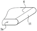
图6是实施方式3涉及的半导体装置的引线端子的弯折部的局部斜视图。
图7是实施方式4涉及的半导体装置的引线端子的局部斜视图。
图8是实施方式4的变形例1涉及的半导体装置的引线端子的局部斜视图。
图9是实施方式4的变形例2涉及的半导体装置的引线端子的局部斜视图。
图10是实施方式5涉及的半导体装置的局部俯视图。
图11是实施方式5涉及的半导体装置的局部剖视图。
图12是实施方式6涉及的半导体装置的局部俯视图。
图13是表示实施方式6涉及的半导体装置的引线端子的构造的局部斜视图。
图14是表示实施方式6的变形例涉及的半导体装置的引线端子的构造的局部斜视图。
图15是表示在实施方式6涉及的半导体装置中进行键合动作的状态的局部俯视图。
图16是表示在实施方式6涉及的半导体装置中进行键合动作的状态的局部剖视图。
图17是表示在实施方式6涉及的半导体装置中没有设置凹陷部的情况下进行键合动作的状态的局部剖视图。
图18是实施方式7涉及的半导体装置的局部斜视图。
图19是实施方式7涉及的半导体装置的局部剖视图。
图20是实施方式8涉及的半导体装置的局部剖视图。
图21是前提技术涉及的半导体装置的概略俯视图。
图22是图21的A-A剖视图。
标号的说明
1半导体元件,3、3a引线端子,5封装树脂,7a凸部,7b凹部,9狭缝,10弯折部,12信号配线,14凹陷部,19端子罩。
具体实施方式
<前提技术>
首先,对前提技术涉及的半导体装置进行说明。图21是前提技术涉及的半导体装置的概略俯视图,图22是图21的A-A剖视图。如图21和图22所示,半导体装置具有半导体元件1、引线端子3、3a、以及封装树脂5。半导体装置还具有绝缘基板4a和壳体4b。半导体元件1的下表面利用焊锡等焊料2接合于在绝缘基板4a的上表面设置的配线图案上。引线端子3、3a使用Cu材料形成为板状,形成为具有沿水平方向延伸的部分的形状。引线端子3、3a利用焊料2连接于半导体元件1的上表面。
壳体4b使用树脂等构成,以将在绝缘基板4a上配置的半导体元件1以及引线端子3、3a的周围包围的方式设置在绝缘基板4a的侧面。在壳体4b的上表面设置端子20,端子20使用穿过壳体4b内的配线与半导体元件1连接。封装树脂5是环氧树脂等,配置在壳体4b内,将半导体元件1与引线端子3、3a一起封装。
在图21中,配置有12个半导体元件1,6个半导体元件1利用3个引线端子3分别以2个为单位进行连接。剩余的6个半导体元件1利用沿水平方向延伸的部分在俯视观察时直线式地延伸的1个引线端子3a连接。
在由于半导体元件1的动作或半导体装置的周围温度的变化而引起的冷热循环中,如果引线端子3a膨胀收缩,则如图22所示,应力向与引线端子3a的端部接触的封装树脂5集中,有可能在封装树脂5中产生裂纹8。尤其是,如果引线端子3a构成为在俯视观察时直线式地延伸,则应力直线式地产生,因此成为裂纹8容易沿引线端子3a传播的状态。在本发明的半导体装置中,通过减小与由冷热循环引起的引线端子3a的膨胀收缩相伴的、对封装树脂5的应力,从而抑制在封装树脂5产生裂纹8。
<实施方式1>
下面,使用附图对本发明的实施方式1进行说明。图1是实施方式1涉及的半导体装置的概略俯视图。此外,在实施方式1中,对与在前提技术中说明的结构要素相同的结构要素标注相同标号而省略说明。
实施方式1涉及的半导体装置是电力用半导体装置,在对车辆的电动机进行控制的逆变器或再生用转换器中使用。另外,半导体元件1例如是由碳化硅(SiC)或氮化镓(GaN)等构成的宽带隙半导体元件。
如图1所示,在实施方式1涉及的半导体装置中,与前提技术相比较,引线端子3a的形状不同。具体而言,引线端子3a具有直线部6、凸部7a以及凹部7b。直线部6是引线端子3a中的沿水平方向延伸的部分在俯视观察时直线式地延伸的部分。凸部7a以向直线部6的宽度方向外侧凸出的方式形成为大致矩形形状。凹部7b设置在引线端子3a中的与凸部7a连续的部分中,以向直线部6的宽度方向内侧凹陷的方式形成为大致矩形形状。直线部6由于凸部7a以及凹部7b而在直线部6的宽度方向(水平方向)上局部地断开。
将多个半导体元件1连接的引线端子3a,为了尽量地减少连续的直线部6,具有大于或等于一组凸部7a以及凹部7b。即使在引线端子3a由于半导体元件1的动作或半导体装置的周围温度的变化而膨胀收缩的情况下,通过在引线端子3a中设置凸部7a以及凹部7b,从而将直线部6局部地断开,能够对在封装树脂5中产生的应力进行分散,抑制裂纹8(参照图22)的传播。
另外,引线端子3、3a使用Cu材料而构成,半导体元件1利用SiC或GaN等而构成。作为封装树脂5采用下述树脂,其线膨胀系数成为引线端子3、3a的线膨胀系数和半导体元件1的线膨胀系数之间的中间值。封装树脂5例如是环氧树脂。由此,抑制封装树脂5与半导体元件1的线膨胀系数差变大,在引线端子3a中产生应力的情况下能够抑制与半导体元件1连接的信号配线被切断。
下面,使用图2,对凸部7a以及凹部7b的尺寸进行说明。图2是实施方式1涉及的半导体装置的局部俯视图,示出凸部7a以及凹部7b的宽度尺寸x和深度尺寸y、与引线端子3a的板厚t之间的关系。凸部7a以及凹部7b以宽度尺寸x以及深度尺寸y大于或等于引线端子3a的板厚t的方式构成。通过将宽度尺寸x或深度尺寸y设为大于或等于板厚t的尺寸,从而在冲压成型等外形造型工序中,能够确保形状稳定性以及制造容易度。
此外,作为焊料2而代表性地使用焊锡,但也可以使用Ag膏或其他导电性连接材料。另外,作为引线端子3、3a,除了Cu材料以外还可以使用Al材料等。
另外,在图1中,引线端子3a具有凸部7a以及凹部7b,但也可以如图3所示,引线端子3a只具有凸部7a。在该情况下,一对凸部7a以向直线部6的宽度方向外侧凸出的方式分别形成为大致矩形形状,引线端子3a具有大于或等于一组成对的凸部7a。图3是实施方式1的变形例1涉及的半导体装置的概略俯视图。
而且,如图4所示,引线端子3a也可以只具有凹部7b。在该情况下,一对凹部7b以向直线部6的宽度方向内侧凹陷的方式分别形成为大致矩形形状,引线端子3a具有大于或等于一组成对的凹部7b。图4是实施方式1的变形例2涉及的半导体装置的概略俯视图。
另外,虽然说明了凸部7a以及凹部7b形成为大致矩形形状,但也可以是多台阶形状、梯形形状、半圆弧形状或者这些形状的组合形状。
如上所示,在实施方式1涉及的半导体装置中,引线端子3a具有将直线式地延伸的部分在水平方向上局部地断开的凹部7b或凸部7a,因此,通过使在引线端子3a中产生的直线式的应力分散,从而能够抑制对封装树脂5的应力,能够抑制在封装树脂5产生裂纹8。另外,引线端子3a具有凹部7b或凸部7a,从而能够抑制在产生裂纹8的情况下的连续性的传播。而且,封装树脂5的线膨胀系数是引线端子3a的线膨胀系数和半导体元件1的线膨胀系数之间的中间值,因此能够抑制封装树脂5与半导体元件1的线膨胀系数差变大,在引线端子3a中产生了应力的情况下,能够抑制与半导体元件1连接的信号配线被切断。由此,能够实现半导体装置的高寿命以及高可靠性。
凹部7b或凸部7a以宽度尺寸x以及深度尺寸y大于或等于引线端子3a的板厚t的方式构成,因此在使得直线式地延伸的部分的局部间断部位变得明显的基础上,还能够取得冲压加工中的形状容易度,并能够延长冲裁模具的寿命。
半导体元件1是可高温动作的宽带隙半导体元件,因此能够针对由来自半导体元件1的发热引起的电极的膨胀,缓和向封装树脂5的应力,能够应对更高温下的产品。
半导体装置是在对车辆的电动机进行控制的逆变器或再生用转换器中使用的电力用半导体装置,因此在要求高品质以及高可靠性的半导体装置中,能够减轻对封装树脂5的损伤,能够确保规定的品质以及可靠性。
<实施方式2>
下面,对实施方式2涉及的半导体装置进行说明。图5是实施方式2涉及的半导体装置的局部俯视图。此外,在实施方式2中,对与在实施方式1中说明的结构要素相同的结构要素标注相同标号而省略说明。
如图5所示,在实施方式2中,在引线端子3a中的与凸部7a或凹部7b连续的部分中设有狭缝9。更具体而言,狭缝9分别设置在引线端子3a中的凸部7a的侧方部分、和引线端子3a的与凹部7b连续的宽度方向内侧部分。另外,狭缝9形成为大致矩形形状,以大于或等于引线端子3a的板厚t的宽度尺寸构成。
通过在引线端子3a中进一步设置狭缝9,从而能够进一步抑制在封装树脂5中产生的直线式的应力的传播。另外,吸收由引线端子3a的热膨胀引起的平面移动变得容易。此外,虽然说明了狭缝9形成为大致矩形形状,但也可以是多台阶形状、梯形形状、圆弧形状或者这些形状的组合形状。在该情况下,也能得到与上述相同的效果。
如上所述,在实施方式2涉及的半导体装置中,引线端子3a在引线端子3a中的与凹部7b或凸部7a连续的部分中还具有狭缝9,该狭缝9以宽度尺寸大于或等于引线端子3a的板厚t的方式构成。因此,在由于引线端子3a的热膨胀而在引线端子3a中发生了长度方向的变形的情况下,能够利用狭缝9吸收引线端子3a的移动,能够进一步抑制在封装树脂5中产生的直线式的应力传播。由此,能够缓和在封装树脂5中产生的应力。另外,即使在将狭缝9设置于引线端子3a中的情况下,也能够在冲压加工中确保加工容易度。
<实施方式3>
下面,对实施方式3涉及的半导体装置进行说明。图6是实施方式3涉及的半导体装置的引线端子3a的弯折部10的局部斜视图。此外,在实施方式3中,对与在实施方式1、2中说明的结构要素相同的结构要素标注相同标号而省略说明。
如图6所示,在实施方式3中,引线端子3a在与凹部7b对应的部分具有弯折部10。弯折部10是将引线端子3a的与凹部7b连续的宽度方向内侧部分向上弯折而形成的。
通过在引线端子3a的与凹部7b连续的宽度方向内侧部分设置向上弯折的弯折部10,从而能够将引线端子3a的直线部6在水平方向以及垂直方向上局部地断开。因此,能够将在封装树脂5中产生的应力分散。另外,通过在引线端子3a中设置弯折部10,从而能够减小由引线端子3a的热膨胀引起的位移量,能够与上述同样地,减小在封装树脂5中产生的应力。并且,通过形成向上侧弯折的弯折部10,从而能够扩宽引线端子3a的下侧的空间,在树脂封装时在将树脂向半导体装置注入时提高树脂的流动性。因此,在封装树脂5中能够消除空隙滞留以及填充不良。
此外,虽然设为引线端子3a的凹部7b是大致矩形形状,但即使是在实施方式1、2中说明的多台阶形状、梯形形状、圆弧形状或者这些形状的组合形状,也能得到同样的效果。另外,在图6中,说明了在引线端子3a的与凹部7b连续的宽度方向内侧部分设置弯折部10,但也能够通过将与图3所示的凸部7a对应的部分、即一对凸部7a和与它们连续的引线端子3a的宽度方向内侧部分向上侧弯折而形成弯折部10。
如上所述,在实施方式3涉及的半导体装置中,引线端子3a在与凹部7b或凸部7a对应的部分中,还具有向上弯折的弯折部10,因此能够将引线端子3a的直线部6在水平方向以及垂直方向上局部地断开,能够抑制在封装树脂5中产生的应力以直线状连锁地产生。另外,能够利用弯折部10进一步吸收由热膨胀引起的引线端子3a的变形。另外,通过向上侧弯折地形成弯折部10,能够加大设计的自由度。由此,能够确保封装树脂5的流动路径,能够提高封装树脂5的封装品质。
<实施方式4>
下面,对实施方式4涉及的半导体装置进行说明。图7是实施方式4涉及的半导体装置的引线端子3a的局部斜视图。此外,在实施方式4中,对与在实施方式1至3中说明的结构要素相同的结构要素标注相同标号而省略说明。
如图7所示,在实施方式4中,引线端子3a的长度方向的端部11形成为台阶形状。更具体而言,引线端子3a的直线部6的长度方向的端部11形成为与上侧部分相比下侧部分的长度方向的长度较短的一层台阶形状。
通过将引线端子3a的直线部6的长度方向的端部11设为台阶形状,从而能够将集中在引线端子3a的长度方向端部的角部处的应力分散至台阶形状的端部11的角部,能够减小在封装树脂5中产生的应力。
如上所述,在实施方式4涉及的半导体装置中,引线端子3a的长度方向的端部11形成为台阶形状,因此,能够缓和由于在引线端子3a的长度方向端部的角部处集中的应力而在封装树脂5中产生的应力。另外,通过将引线端子3a的直线部6的长度方向的端部11设为台阶形状,从而能够在引线端子3a的端部11处确保规定的树脂厚度,因此能够提高封装树脂5的树脂强度,并且能够在树脂封装时确保向引线端子3a的端部11的树脂流动性。
此外,在图7中,例示出一层台阶形状,但也可以是多层。另外,如图8所示,也可以是引线端子3a的直线部6的长度方向的端部11形成为圆弧形状,或者如图9所示,形成为倒角形状。在这里,图8是实施方式4的变形例1涉及的半导体装置的引线端子3a的局部斜视图,图9是实施方式4的变形例2涉及的半导体装置的引线端子3a的局部斜视图。在上述情况下也能得到与上述同样的效果。
<实施方式5>
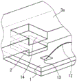
下面,对实施方式5涉及的半导体装置进行说明。图10是实施方式5涉及的半导体装置的局部俯视图,图11是实施方式5涉及的半导体装置的局部剖视图。此外,在实施方式5中,对与在实施方式1至4中说明的结构要素相同的结构要素标注相同标号而省略说明。
如图10所示,在实施方式5中,引线端子3a形成为,将半导体元件1的上表面中的、除了与信号配线12连接的部分即导线键合焊盘13以外的整个上表面覆盖。更具体而言,在实施方式5中引线端子3a形成为,与实施方式1至4的情况相比在俯视观察时的轮廓较大。另外,在引线端子3a中的与导线键合焊盘13相对应的位置处设置有凹部7c,以使导线键合焊盘13露出。
如图10所示,通过利用引线端子3a覆盖半导体元件1的上表面,从而由于引线端子3a的热膨胀而从引线端子3a的端部向封装树脂5施加应力。如图11所示,即使万一产生了裂纹8,也能够避免向半导体元件1上的传播。另外,为了仅露出导线键合焊盘13,在引线端子3a中的与导线键合焊盘13对应的位置设置凹部7c,因此能够将引线端子3a的直线部6在水平方向上局部地进一步断开。
如上所述,在实施方式5涉及的半导体装置中,引线端子3a形成为将半导体元件1的上表面中的、除了与信号配线12连接的部分以外的整个上表面覆盖,因此,即使在由于通过引线端子3a的热膨胀引起的应力而在封装树脂5中产生了裂纹8的情况下,也能够利用引线端子3a抑制裂纹8在半导体元件1的上表面侧加深,抑制对半导体元件1的损伤。另外,与实施方式1至4的情况相比,通过将引线端子3a设为较大,从而能够使电流密度下降,降低引线端子3a的发热量,减小由热膨胀引起的影响。
<实施方式6>
下面,对实施方式6涉及的半导体装置进行说明。图12是实施方式6涉及的半导体装置的局部俯视图,图13是表示实施方式6涉及的半导体装置的引线端子3a的构造的局部斜视图。此外,在实施方式6中,对与在实施方式1至5中说明的结构要素相同的结构要素标注相同标号而省略说明。
如图12和图13所示,在实施方式6中,引线端子3a还具有凹陷部14,该凹陷部14是向半导体元件1的上表面中的与信号配线12所连接的部分(存在导线键合焊盘13的部分)邻接的上表面侧以台阶状凹陷而设置的。更具体而言,凹陷部14是在引线端子3a中的与导线键合焊盘13露出的部分即凹部7c邻接的位置以台阶状凹陷而设置的。
在图13中,在引线端子3a中仅使成为凹陷部14的平面部凹陷而形成凹陷部14,但也可以如图14所示,通过进行半切(half-cut)而形成台阶状的凹陷部14。在这里,图14是表示实施方式6的变形例涉及的半导体装置的引线端子3a的构造的局部斜视图。此外,在图13和图14中,为了使附图容易观察,而省略引线端子3a中的从凹陷部14起的、凹部7c侧的部分而未图示。
下面,对实施方式6涉及的半导体装置的作用、效果进行说明。图15是表示在实施方式6涉及的半导体装置中进行键合动作的状态的局部俯视图,图16是表示在实施方式6涉及的半导体装置中进行键合动作的状态的局部剖视图,图17是表示在实施方式6涉及的半导体装置中没有设置凹陷部14的情况下进行键合动作的状态的局部剖视图。
如图15和图16所示,在进行利用楔形工具16实现的键合动作的状态下,楔形工具16的侧部位于在引线端子3a中设置的台阶状的凹陷部14中,因此能够避免引线端子3a与楔形工具16的干涉。
另一方面,如图17所示,在引线端子3a中没有设置凹陷部14的情况下,从引线端子3a的侧面至导线键合焊盘13为止的距离的关系成为c<d。即,表示在与设置有凹陷部14的情况相同的位置关系下,楔形工具16会与引线端子3a干涉。在这里,c是在设置有凹陷部14的情况下从引线端子3a的侧面至导线键合焊盘13为止的距离,d是在没有设置凹陷部14的情况下从引线端子3a的侧面至导线键合焊盘13为止的距离。
通过在引线端子3a中设置凹陷部14,从而能够避免引线端子3a与楔形工具16的干涉,因此,能够将凹部7c设为最小限度的大小,能够扩大利用引线端子3a覆盖半导体元件1的面积。另外,能够利用凹陷部14将引线端子3a的直线部6局部地断开,能够抑制在封装树脂5中产生的应力的传播。
如上所述,在实施方式6涉及的半导体装置中,引线端子3a还具有凹陷部14,该凹陷部14是向半导体元件1的上表面中的、与信号配线12所连接的部分邻接的上表面侧以台阶状凹陷而设置的。因此,能够将凹部7c设为最小限度的大小。另外,在对凹陷部14进行了半切的情况下,能够将引线端子3a整体从绝缘基板4a分离,因此,能够通过将引线端子3a和绝缘基板4a的间隙扩宽而确保树脂流动性。
<实施方式7>
下面,对实施方式7涉及的半导体装置进行说明。图18是实施方式7涉及的半导体装置的局部斜视图,图19是表示实施方式7涉及的半导体装置的局部剖视图。此外,在实施方式7中,对与在实施方式1至6中说明的结构要素相同的结构要素标注相同标号而省略说明。
如图18所示,在实施方式7中,对引线端子3a中的与半导体元件1连接的部分的侧面实施使焊料2的浸润性提高的表面处理。该表面处理是例如是镀Ni的处理,在引线端子3a中的与半导体元件1连接的部分的侧面形成有Ni薄膜17。在这里,表面处理除了镀Ni的处理之外,也可以是镀Au、镀Ag或助焊剂等处理。而且,表面处理也可以是化学研磨等表面改质的处理。
如图19所示,通过提高引线端子3a中的与半导体元件1连接的部分的侧面的浸润性,从而用于将半导体元件1接合的焊料2浸润攀升至该侧面。焊料2与封装树脂5密接性较低,因此在焊料2和封装树脂5之间形成界面18,由此能够对在封装树脂5中产生的应力进行分散。
如上所述,在实施方式7涉及的半导体装置中,对引线端子3a中的与半导体元件1连接的部分的侧面实施使浸润性提高的表面处理,因此,用于将半导体元件1接合的焊料2浸润攀升至该侧面,引线端子3a的该侧面与封装树脂5之间的密接性下降。由此,能够将由引线端子3a的热膨胀引起的位移与封装树脂5隔离开,降低在封装树脂5中产生的应力。
<实施方式8>
下面,对实施方式8涉及的半导体装置进行说明。图20是实施方式8涉及的半导体装置的局部剖视图。此外,在实施方式8中,对与在实施方式1至7中说明的结构要素相同的结构要素标注相同标号而省略说明。
如图20所示,在实施方式8中,半导体装置还具有端子罩19,该端子罩19对引线端子3a中的与半导体元件1连接的部分的侧面进行覆盖。更具体而言,端子罩19利用Teflon(注册商标)树脂形成为U字形状,安装于引线端子3a的、包含与半导体元件1连接的部分的侧面在内的侧部。在这里,端子罩19除了Teflon(注册商标)树脂以外,也能够使用ABS、PC、PS或PPS等热塑性树脂、或者SUS304等金属材料构成。
通过在引线端子3a的侧部安装端子罩19后,填充封装树脂5,从而能够将引线端子3a的热膨胀或收缩的位移与封装树脂5隔离开。因此,能够使传播至封装树脂5的应力成为最小限。由此,得到抑制封装树脂5产生裂纹8的效果。另外,以碳化硅为主的半导体装置能够在更高温度下动作。即,能够将封装树脂5设为良好的封装状态,因此能够提供可靠性更优异的半导体装置。
如上所述,实施方式8涉及的半导体装置还具有端子罩19,该端子罩19对引线端子3a中的与半导体元件1连接的部分的侧面进行覆盖,因此,有意图地在引线端子3a和封装树脂5之间形成界面,从而能够减小对封装树脂5施加的应力。
此外,本发明能够在其发明的范围内,对各实施方式自由地进行组合,或对各实施方式适当进行变形、省略。
Claims (16)
1.一种半导体装置,其具有:
半导体元件,其下表面与基板侧接合;
引线端子,其与所述半导体元件的上表面接合,该引线端子的长度方向的端部的形状形成为,与上侧部分相比下侧部分的长度方向的长度较短的台阶形状;以及
封装树脂,其将所述半导体元件与所述引线端子的所述台阶形状的部分一起进行封装,
所述引线端子形成为,将所述半导体元件的所述上表面中的、除了与信号配线连接的部分之外的整个上表面覆盖。
2.一种半导体装置,其具有:
半导体元件,其下表面与基板侧接合;
引线端子,其与所述半导体元件的上表面接合,该引线端子的长度方向的端部的形状形成为,与上侧部分相比下侧部分的长度方向的长度较短的台阶形状;以及
封装树脂,其将所述半导体元件与所述引线端子的所述台阶形状的部分一起进行封装,
所述引线端子具有沿水平方向延伸的部分,
所述引线端子的所述沿水平方向延伸的部分包含与所述半导体元件接合且在俯视观察时直线式地延伸的部分,
所述引线端子具有将所述直线式地延伸的部分在俯视观察时局部地断开的凹部或凸部,
所述引线端子形成为,将所述半导体元件的所述上表面中的、除了与信号配线连接的部分之外的整个上表面覆盖。
3.一种半导体装置,其具有:
半导体元件,其下表面与基板侧接合;
引线端子,其与所述半导体元件的上表面接合,该引线端子的长度方向的端部的形状形成为,与上侧部分相比下侧部分的长度方向的长度较短的多层台阶形状;以及
封装树脂,其将所述半导体元件与所述引线端子的所述多层台阶形状的部分一起进行封装,
所述引线端子形成为,将所述半导体元件的所述上表面中的、除了与信号配线连接的部分之外的整个上表面覆盖。
4.一种半导体装置,其具有:
半导体元件,其下表面与基板侧接合;
引线端子,其与所述半导体元件的上表面接合,该引线端子的长度方向的端部的形状形成为圆弧形状;以及
封装树脂,其将所述半导体元件与所述引线端子的所述圆弧形状的部分一起进行封装,
所述引线端子形成为,将所述半导体元件的所述上表面中的、除了与信号配线连接的部分之外的整个上表面覆盖。
5.一种半导体装置,其具有:
半导体元件,其下表面与基板侧接合;
引线端子,其与所述半导体元件的上表面接合,该引线端子的长度方向的端部的形状形成为倒角形状;以及
封装树脂,其将所述半导体元件与所述引线端子的所述倒角形状的部分一起进行封装,
所述引线端子形成为,将所述半导体元件的所述上表面中的、除了与信号配线连接的部分之外的整个上表面覆盖。
6.根据权利要求1至5中任一项所述的半导体装置,其中,
所述封装树脂的线膨胀系数是所述引线端子的线膨胀系数和所述半导体元件的线膨胀系数之间的中间值。
7.根据权利要求2所述的半导体装置,其中,
所述凹部或所述凸部以宽度以及深度大于或等于所述引线端子的厚度的方式构成。
8.根据权利要求2或7所述的半导体装置,其中,
所述引线端子在所述引线端子中的与所述凹部或所述凸部连续的部分,还具有以宽度大于或等于所述引线端子的厚度的方式构成的狭缝。
9.根据权利要求2、7中任一项所述的半导体装置,其中,
所述引线端子在与所述凹部或所述凸部对应的部分,还具有向上弯折的弯折部。
10.一种半导体装置,其具有:
半导体元件,其下表面与基板侧接合;
引线端子,其与所述半导体元件的上表面接合;以及
封装树脂,其将所述半导体元件与所述引线端子的接合于所述半导体元件的部分一起进行封装,
所述封装树脂的线膨胀系数是所述引线端子的线膨胀系数和所述半导体元件的线膨胀系数之间的中间值,
所述引线端子形成为,将所述半导体元件的所述上表面中的、除了与信号配线连接的部分之外的整个上表面覆盖,
所述引线端子还具有凹陷部,该凹陷部是向所述半导体元件的所述上表面中的、与信号配线所连接的部分邻接的所述上表面侧以台阶状凹陷而设置的。
11.一种半导体装置,其具有:
半导体元件,其下表面与基板侧接合;
引线端子,其与所述半导体元件的上表面接合,该引线端子的长度方向的端部的形状形成为,与上侧部分相比下侧部分的长度方向的长度较短的台阶形状;以及
封装树脂,其将所述半导体元件与所述引线端子的所述台阶形状的部分一起进行封装,
所述引线端子形成为,将所述半导体元件的所述上表面中的、除了与信号配线连接的部分之外的整个上表面覆盖,
所述引线端子还具有凹陷部,该凹陷部是向所述半导体元件的所述上表面中的、与信号配线所连接的部分邻接的所述上表面侧以台阶状凹陷而设置的。
12.根据权利要求1至5、10、11中任一项所述的半导体装置,其中,
对所述引线端子中的与所述半导体元件连接的部分的侧面实施使浸润性提高的表面处理。
13.一种半导体装置,其具有:
半导体元件,其下表面与基板侧接合;
引线端子,其与所述半导体元件的上表面接合;以及
封装树脂,其将所述半导体元件与所述引线端子的接合于所述半导体元件的部分一起进行封装,
所述封装树脂的线膨胀系数是所述引线端子的线膨胀系数和所述半导体元件的线膨胀系数之间的中间值,
还具有端子罩,该端子罩覆盖所述引线端子中的与所述半导体元件连接的部分的侧面。
14.一种半导体装置,其具有:
半导体元件,其下表面与基板侧接合;
引线端子,其与所述半导体元件的上表面接合,该引线端子的长度方向的端部的形状形成为,与上侧部分相比下侧部分的长度方向的长度较短的台阶形状;以及
封装树脂,其将所述半导体元件与所述引线端子的所述台阶形状的部分一起进行封装,
还具有端子罩,该端子罩覆盖所述引线端子中的与所述半导体元件连接的部分的侧面。
15.根据权利要求1至5、10、11、13、14中任一项所述的半导体装置,其中,
所述半导体元件是宽带隙半导体元件。
16.根据权利要求1至5、10、11、13、14中任一项所述的半导体装置,其中,
所述半导体装置是在对车辆的电动机进行控制的逆变器或再生用转换器中使用的电力用半导体装置。
Applications Claiming Priority (3)
| Application Number | Priority Date | Filing Date | Title |
|---|---|---|---|
| JP2014-211424 | 2014-10-16 | ||
| JP2014211424A JP6385234B2 (ja) | 2014-10-16 | 2014-10-16 | 半導体装置 |
| CN201510673980.6A CN105529319B (zh) | 2014-10-16 | 2015-10-16 | 半导体装置 |
Related Parent Applications (1)
| Application Number | Title | Priority Date | Filing Date |
|---|---|---|---|
| CN201510673980.6A Division CN105529319B (zh) | 2014-10-16 | 2015-10-16 | 半导体装置 |
Publications (2)
| Publication Number | Publication Date |
|---|---|
| CN106952877A CN106952877A (zh) | 2017-07-14 |
| CN106952877B true CN106952877B (zh) | 2021-01-01 |
Family
ID=55638195
Family Applications (3)
| Application Number | Title | Priority Date | Filing Date |
|---|---|---|---|
| CN201611055874.2A Active CN106952877B (zh) | 2014-10-16 | 2015-10-16 | 半导体装置 |
| CN201910281594.0A Active CN110071072B (zh) | 2014-10-16 | 2015-10-16 | 半导体装置 |
| CN201510673980.6A Active CN105529319B (zh) | 2014-10-16 | 2015-10-16 | 半导体装置 |
Family Applications After (2)
| Application Number | Title | Priority Date | Filing Date |
|---|---|---|---|
| CN201910281594.0A Active CN110071072B (zh) | 2014-10-16 | 2015-10-16 | 半导体装置 |
| CN201510673980.6A Active CN105529319B (zh) | 2014-10-16 | 2015-10-16 | 半导体装置 |
Country Status (4)
| Country | Link |
|---|---|
| US (1) | US9917064B2 (zh) |
| JP (1) | JP6385234B2 (zh) |
| CN (3) | CN106952877B (zh) |
| DE (1) | DE102015215786A1 (zh) |
Families Citing this family (11)
| Publication number | Priority date | Publication date | Assignee | Title |
|---|---|---|---|---|
| US10204847B2 (en) * | 2016-10-06 | 2019-02-12 | Infineon Technologies Americas Corp. | Multi-phase common contact package |
| US10770376B2 (en) | 2016-11-11 | 2020-09-08 | Mitsubishi Electric Corporation | Semiconductor device, inverter unit and automobile |
| JP6776840B2 (ja) * | 2016-11-21 | 2020-10-28 | オムロン株式会社 | 電子装置およびその製造方法 |
| JP6806170B2 (ja) * | 2017-02-09 | 2021-01-06 | 三菱電機株式会社 | 半導体装置及び電力変換装置 |
| US10896868B2 (en) * | 2017-02-20 | 2021-01-19 | Shindengen Electric Manufacturing Co., Ltd. | Electronic device and connector |
| US11257768B2 (en) * | 2017-12-13 | 2022-02-22 | Mitsubishi Electric Corporation | Semiconductor device and power conversion device |
| WO2019215806A1 (ja) * | 2018-05-08 | 2019-11-14 | 三菱電機株式会社 | 配線部材及びこれを備えた半導体モジュール |
| CN112567504B (zh) * | 2018-11-30 | 2024-08-20 | 株式会社博迈立铖 | 电连接用部件、电连接结构和电连接用结构的制造方法 |
| US11387210B2 (en) * | 2019-03-15 | 2022-07-12 | Fuji Electric Co., Ltd. | Semiconductor module and manufacturing method therefor |
| JP7301805B2 (ja) * | 2020-09-24 | 2023-07-03 | 株式会社東芝 | 半導体モジュール |
| JPWO2023203688A1 (zh) * | 2022-04-20 | 2023-10-26 |
Citations (7)
| Publication number | Priority date | Publication date | Assignee | Title |
|---|---|---|---|---|
| CN1988137A (zh) * | 2005-12-19 | 2007-06-27 | 三菱电机株式会社 | 半导体装置 |
| JP2007173703A (ja) * | 2005-12-26 | 2007-07-05 | Mitsubishi Electric Corp | 半導体装置 |
| JP2010147053A (ja) * | 2008-12-16 | 2010-07-01 | Fuji Electric Systems Co Ltd | 半導体装置 |
| CN102593091A (zh) * | 2011-01-14 | 2012-07-18 | 丰田自动车株式会社 | 半导体模块 |
| CN103545268A (zh) * | 2012-07-09 | 2014-01-29 | 万国半导体股份有限公司 | 底部源极的功率器件及制备方法 |
| CN103843135A (zh) * | 2011-09-29 | 2014-06-04 | 丰田自动车株式会社 | 半导体装置 |
| CN103972276A (zh) * | 2013-02-06 | 2014-08-06 | 三菱电机株式会社 | 半导体装置及其制造方法 |
Family Cites Families (17)
| Publication number | Priority date | Publication date | Assignee | Title |
|---|---|---|---|---|
| JPH01276655A (ja) | 1988-04-27 | 1989-11-07 | Japan Radio Co Ltd | トランスファーモールド型集積回路 |
| JPH065742A (ja) | 1992-06-22 | 1994-01-14 | Mitsubishi Electric Corp | 半導体装置、その封止に用いられる樹脂および半導体装置の製造方法 |
| JPH06120406A (ja) | 1992-10-02 | 1994-04-28 | Mitsubishi Electric Corp | 半導体装置 |
| JP3866880B2 (ja) | 1999-06-28 | 2007-01-10 | 株式会社日立製作所 | 樹脂封止型電子装置 |
| JP2005012085A (ja) * | 2003-06-20 | 2005-01-13 | Toyota Motor Corp | 半導体モジュールの電極構造 |
| JP4628687B2 (ja) * | 2004-03-09 | 2011-02-09 | ルネサスエレクトロニクス株式会社 | 半導体装置 |
| JP4468115B2 (ja) * | 2004-08-30 | 2010-05-26 | 株式会社ルネサステクノロジ | 半導体装置 |
| CN100442483C (zh) | 2004-09-16 | 2008-12-10 | 夏普株式会社 | 半导体光器件、其制造方法、引线框以及电子设备 |
| DE102005043928B4 (de) * | 2004-09-16 | 2011-08-18 | Sharp Kk | Optisches Halbleiterbauteil und Verfahren zu dessen Herstellung |
| TWI280673B (en) * | 2004-09-22 | 2007-05-01 | Sharp Kk | Optical semiconductor device, optical communication device, and electronic equipment |
| JP4348267B2 (ja) | 2004-09-22 | 2009-10-21 | シャープ株式会社 | 光半導体装置、光通信装置および電子機器 |
| JP4492448B2 (ja) | 2005-06-15 | 2010-06-30 | 株式会社日立製作所 | 半導体パワーモジュール |
| JP2008016529A (ja) * | 2006-07-04 | 2008-01-24 | Renesas Technology Corp | 半導体装置 |
| JP2008218688A (ja) * | 2007-03-05 | 2008-09-18 | Denso Corp | 半導体装置 |
| JP5384913B2 (ja) * | 2008-11-18 | 2014-01-08 | ルネサスエレクトロニクス株式会社 | 半導体装置およびその製造方法 |
| JP5665572B2 (ja) | 2011-01-28 | 2015-02-04 | 三菱電機株式会社 | 半導体装置および半導体装置の製造方法 |
| JP2013197573A (ja) | 2012-03-23 | 2013-09-30 | Mitsubishi Electric Corp | 半導体装置 |
-
2014
- 2014-10-16 JP JP2014211424A patent/JP6385234B2/ja active Active
-
2015
- 2015-07-02 US US14/790,682 patent/US9917064B2/en active Active
- 2015-08-19 DE DE102015215786.5A patent/DE102015215786A1/de active Pending
- 2015-10-16 CN CN201611055874.2A patent/CN106952877B/zh active Active
- 2015-10-16 CN CN201910281594.0A patent/CN110071072B/zh active Active
- 2015-10-16 CN CN201510673980.6A patent/CN105529319B/zh active Active
Patent Citations (7)
| Publication number | Priority date | Publication date | Assignee | Title |
|---|---|---|---|---|
| CN1988137A (zh) * | 2005-12-19 | 2007-06-27 | 三菱电机株式会社 | 半导体装置 |
| JP2007173703A (ja) * | 2005-12-26 | 2007-07-05 | Mitsubishi Electric Corp | 半導体装置 |
| JP2010147053A (ja) * | 2008-12-16 | 2010-07-01 | Fuji Electric Systems Co Ltd | 半導体装置 |
| CN102593091A (zh) * | 2011-01-14 | 2012-07-18 | 丰田自动车株式会社 | 半导体模块 |
| CN103843135A (zh) * | 2011-09-29 | 2014-06-04 | 丰田自动车株式会社 | 半导体装置 |
| CN103545268A (zh) * | 2012-07-09 | 2014-01-29 | 万国半导体股份有限公司 | 底部源极的功率器件及制备方法 |
| CN103972276A (zh) * | 2013-02-06 | 2014-08-06 | 三菱电机株式会社 | 半导体装置及其制造方法 |
Also Published As
| Publication number | Publication date |
|---|---|
| CN110071072A (zh) | 2019-07-30 |
| CN105529319A (zh) | 2016-04-27 |
| US20160111379A1 (en) | 2016-04-21 |
| DE102015215786A1 (de) | 2016-04-21 |
| US9917064B2 (en) | 2018-03-13 |
| JP6385234B2 (ja) | 2018-09-05 |
| CN106952877A (zh) | 2017-07-14 |
| CN110071072B (zh) | 2023-12-01 |
| JP2016082048A (ja) | 2016-05-16 |
| CN105529319B (zh) | 2019-04-26 |
Similar Documents
| Publication | Publication Date | Title |
|---|---|---|
| CN106952877B (zh) | 半导体装置 | |
| JP6234630B2 (ja) | パワーモジュール | |
| US9153519B2 (en) | Semiconductor device for preventing a progression of a crack in a solder layer and method of manufacturing the same | |
| JP6293030B2 (ja) | 電力用半導体装置 | |
| JP6316412B2 (ja) | 電力用半導体装置 | |
| US20160300770A1 (en) | Power module and method of manufacturing power module | |
| US10763240B2 (en) | Semiconductor device comprising signal terminals extending from encapsulant | |
| EP2717310A1 (en) | Semiconductor device and wiring substrate | |
| JP2016018866A (ja) | パワーモジュール | |
| JP4530863B2 (ja) | 樹脂封止型半導体装置 | |
| JP2015115471A (ja) | 電力用半導体装置 | |
| WO2021002132A1 (ja) | 半導体モジュールの回路構造 | |
| WO2015125772A1 (ja) | 電極リードおよび半導体装置 | |
| JP2008016469A (ja) | 半導体装置 | |
| JP5368357B2 (ja) | 電極部材およびこれを用いた半導体装置 | |
| CN110892526B (zh) | 半导体装置的制造方法 | |
| WO2022070741A1 (ja) | 半導体装置 | |
| US11302612B2 (en) | Lead frame wiring structure and semiconductor module | |
| KR101561920B1 (ko) | 반도체 패키지 | |
| US11823985B2 (en) | Leadframe, semiconductor device, and method for manufacturing semiconductor device | |
| US11646250B2 (en) | Semiconductor device | |
| JP6416055B2 (ja) | 半導体装置 | |
| CN110892527A (zh) | 半导体装置以及半导体装置的制造方法 | |
| CN111316429A (zh) | 半导体装置 | |
| JP2015167171A (ja) | 半導体装置 |
Legal Events
| Date | Code | Title | Description |
|---|---|---|---|
| PB01 | Publication | ||
| PB01 | Publication | ||
| SE01 | Entry into force of request for substantive examination | ||
| SE01 | Entry into force of request for substantive examination | ||
| GR01 | Patent grant | ||
| GR01 | Patent grant |