WO2023176538A1 - 積層セラミックコンデンサ - Google Patents
積層セラミックコンデンサ Download PDFInfo
- Publication number
- WO2023176538A1 WO2023176538A1 PCT/JP2023/008255 JP2023008255W WO2023176538A1 WO 2023176538 A1 WO2023176538 A1 WO 2023176538A1 JP 2023008255 W JP2023008255 W JP 2023008255W WO 2023176538 A1 WO2023176538 A1 WO 2023176538A1
- Authority
- WO
- WIPO (PCT)
- Prior art keywords
- via conductor
- multilayer ceramic
- capacitor body
- external electrode
- capacitor
- Prior art date
- Legal status (The legal status is an assumption and is not a legal conclusion. Google has not performed a legal analysis and makes no representation as to the accuracy of the status listed.)
- Ceased
Links
Images


Classifications
-
- H—ELECTRICITY
- H01—ELECTRIC ELEMENTS
- H01G—CAPACITORS; CAPACITORS, RECTIFIERS, DETECTORS, SWITCHING DEVICES, LIGHT-SENSITIVE OR TEMPERATURE-SENSITIVE DEVICES OF THE ELECTROLYTIC TYPE
- H01G4/00—Fixed capacitors; Processes of their manufacture
- H01G4/30—Stacked capacitors
-
- H—ELECTRICITY
- H01—ELECTRIC ELEMENTS
- H01G—CAPACITORS; CAPACITORS, RECTIFIERS, DETECTORS, SWITCHING DEVICES, LIGHT-SENSITIVE OR TEMPERATURE-SENSITIVE DEVICES OF THE ELECTROLYTIC TYPE
- H01G4/00—Fixed capacitors; Processes of their manufacture
- H01G4/002—Details
- H01G4/005—Electrodes
- H01G4/008—Selection of materials
-
- H—ELECTRICITY
- H01—ELECTRIC ELEMENTS
- H01G—CAPACITORS; CAPACITORS, RECTIFIERS, DETECTORS, SWITCHING DEVICES, LIGHT-SENSITIVE OR TEMPERATURE-SENSITIVE DEVICES OF THE ELECTROLYTIC TYPE
- H01G4/00—Fixed capacitors; Processes of their manufacture
- H01G4/002—Details
- H01G4/005—Electrodes
- H01G4/012—Form of non-self-supporting electrodes
-
- H—ELECTRICITY
- H01—ELECTRIC ELEMENTS
- H01G—CAPACITORS; CAPACITORS, RECTIFIERS, DETECTORS, SWITCHING DEVICES, LIGHT-SENSITIVE OR TEMPERATURE-SENSITIVE DEVICES OF THE ELECTROLYTIC TYPE
- H01G4/00—Fixed capacitors; Processes of their manufacture
- H01G4/002—Details
- H01G4/018—Dielectrics
- H01G4/06—Solid dielectrics
- H01G4/08—Inorganic dielectrics
- H01G4/12—Ceramic dielectrics
- H01G4/1209—Ceramic dielectrics characterised by the ceramic dielectric material
- H01G4/1218—Ceramic dielectrics characterised by the ceramic dielectric material based on titanium oxides or titanates
- H01G4/1227—Ceramic dielectrics characterised by the ceramic dielectric material based on titanium oxides or titanates based on alkaline earth titanates
-
- H—ELECTRICITY
- H01—ELECTRIC ELEMENTS
- H01G—CAPACITORS; CAPACITORS, RECTIFIERS, DETECTORS, SWITCHING DEVICES, LIGHT-SENSITIVE OR TEMPERATURE-SENSITIVE DEVICES OF THE ELECTROLYTIC TYPE
- H01G4/00—Fixed capacitors; Processes of their manufacture
- H01G4/002—Details
- H01G4/018—Dielectrics
- H01G4/06—Solid dielectrics
- H01G4/08—Inorganic dielectrics
- H01G4/12—Ceramic dielectrics
- H01G4/1209—Ceramic dielectrics characterised by the ceramic dielectric material
- H01G4/1236—Ceramic dielectrics characterised by the ceramic dielectric material based on zirconium oxides or zirconates
-
- H—ELECTRICITY
- H01—ELECTRIC ELEMENTS
- H01G—CAPACITORS; CAPACITORS, RECTIFIERS, DETECTORS, SWITCHING DEVICES, LIGHT-SENSITIVE OR TEMPERATURE-SENSITIVE DEVICES OF THE ELECTROLYTIC TYPE
- H01G4/00—Fixed capacitors; Processes of their manufacture
- H01G4/002—Details
- H01G4/228—Terminals
- H01G4/232—Terminals electrically connecting two or more layers of a stacked or rolled capacitor
-
- H—ELECTRICITY
- H01—ELECTRIC ELEMENTS
- H01G—CAPACITORS; CAPACITORS, RECTIFIERS, DETECTORS, SWITCHING DEVICES, LIGHT-SENSITIVE OR TEMPERATURE-SENSITIVE DEVICES OF THE ELECTROLYTIC TYPE
- H01G4/00—Fixed capacitors; Processes of their manufacture
- H01G4/002—Details
- H01G4/228—Terminals
- H01G4/236—Terminals leading through the housing, i.e. lead-through
-
- Y—GENERAL TAGGING OF NEW TECHNOLOGICAL DEVELOPMENTS; GENERAL TAGGING OF CROSS-SECTIONAL TECHNOLOGIES SPANNING OVER SEVERAL SECTIONS OF THE IPC; TECHNICAL SUBJECTS COVERED BY FORMER USPC CROSS-REFERENCE ART COLLECTIONS [XRACs] AND DIGESTS
- Y02—TECHNOLOGIES OR APPLICATIONS FOR MITIGATION OR ADAPTATION AGAINST CLIMATE CHANGE
- Y02E—REDUCTION OF GREENHOUSE GAS [GHG] EMISSIONS, RELATED TO ENERGY GENERATION, TRANSMISSION OR DISTRIBUTION
- Y02E60/00—Enabling technologies; Technologies with a potential or indirect contribution to GHG emissions mitigation
- Y02E60/13—Energy storage using capacitors
Definitions
- the present invention relates to a multilayer ceramic capacitor.
- Multilayer capacitors are known in which the ESL (equivalent series inductance) is reduced by making the current flow route thicker, the current flow route shorter, or the magnetic fields generated by currents with different polarities canceling each other out.
- Patent Document 1 discloses an example of a multilayer capacitor with a reduced ESL.
- the multilayer capacitor 200 disclosed in Patent Document 1 includes a plurality of dielectric layers 201, a plurality of first internal electrodes 202, and a plurality of second internal electrodes 202. It includes a capacitor body 210 in which internal electrodes 203 are laminated.
- the capacitor body 210 includes a plurality of first via conductors 204 that are electrically connected to the plurality of first internal electrodes 202 and extend to one main surface of the capacitor body 210, and a plurality of second internal electrodes. 203 and a plurality of second via conductors 205 extending to one main surface of the capacitor body 210.
- a plurality of first external electrodes 211 are electrically connected to the plurality of first via conductors 204, respectively, and a plurality of second external electrodes 211 are electrically connected to the plurality of second via conductors 205, respectively.
- a plurality of second external electrodes 212 are formed.
- the plurality of first external electrodes 211 and the plurality of second external electrodes 212 are arranged in a grid pattern, as shown in FIG.
- the second via conductors 205 are also arranged in a grid pattern.
- the first internal electrode 202 and the second internal electrode 203 face each other. The area is reduced and the capacitance is reduced.
- the present invention solves the above problems, and aims to provide a multilayer ceramic capacitor that can increase capacitance compared to conventional multilayer ceramic capacitors in which via conductors are arranged in a grid pattern. do.
- the multilayer ceramic capacitor of the present invention is a capacitor body in which a plurality of dielectric layers, a plurality of first internal electrodes, and a plurality of second internal electrodes are laminated; a first via conductor provided inside the capacitor body and electrically connected to the plurality of first internal electrodes; a second via conductor provided inside the capacitor body and electrically connected to the plurality of second internal electrodes; a first external electrode provided on the surface of the capacitor body and electrically connected to the first via conductor; a second external electrode provided on the surface of the capacitor body and electrically connected to the second via conductor; Equipped with When the capacitor body is viewed in the stacking direction of the dielectric layer, the first internal electrode, and the second internal electrode, m ⁇ n (m and n are each natural numbers of 3 or more) virtual lattice points.
- the innermost virtual grid point is located at the outermost periphery.
- the first via conductor and the second via conductor are not arranged at the virtual lattice points of 1 or more (m-2) ⁇ (n-2) or less located at .
- the capacitance is can be increased.
- FIG. 1 is a plan view schematically showing a multilayer ceramic capacitor in an embodiment of the present invention.
- FIG. 2 is a cross-sectional view schematically showing the structure of the multilayer ceramic capacitor shown in FIG. 1 taken along line II-II.
- FIG. 2 is a cross-sectional view schematically showing the structure of the multilayer ceramic capacitor shown in FIG. 1 taken along line III-III.
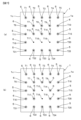
- FIG. 3 is a diagram for explaining a standard arrangement in which via conductors are arranged at all m ⁇ n virtual grid points.
- FIG. 3 is a diagram showing the arrangement positions of a first via conductor and a second via conductor of a multilayer ceramic capacitor in one embodiment.
- FIG. 3 is a diagram showing an equivalent circuit of two multilayer ceramic capacitors connected in parallel to a power supply line.
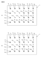
- FIG. 6 is a diagram illustrating an example of a configuration in which no conductor is arranged.
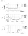
- FIG. 2 is a diagram showing the results of measuring the electrical characteristics of a multilayer ceramic capacitor in one embodiment, a multilayer ceramic capacitor in Comparative Example 1, and a multilayer ceramic capacitor in Comparative Example 2, in which (a) shows the capacitance; (b) ) indicates ESR, and (c) indicates ESL.
- (a) is a perspective view schematically showing the multilayer capacitor described in Patent Document 1
- (b) is a schematic perspective view of the structure when the multilayer capacitor shown in (a) is cut along the XB-XB line.
- FIG. 1 is a plan view schematically showing a multilayer ceramic capacitor 100 in an embodiment of the present invention.
- FIG. 2 is a cross-sectional view schematically showing the structure of the multilayer ceramic capacitor 100 shown in FIG. 1 taken along line II-II.
- FIG. 3 is a cross-sectional view schematically showing the structure of the multilayer ceramic capacitor 100 shown in FIG. 1 taken along line III-III.
- the multilayer ceramic capacitor 100 includes a capacitor body 1 , a first via conductor 5 , a second via conductor 6 , a first external electrode 11 , and a second external electrode 12 .
- the capacitor body 1 has a structure in which a plurality of dielectric layers 2, a plurality of first internal electrodes 3, and a plurality of second internal electrodes 4 are laminated. More specifically, the capacitor body 1 has a structure in which a plurality of first internal electrodes 3 and second internal electrodes 4 are alternately stacked with dielectric layers 2 in between.
- the material of the dielectric layer 2 is arbitrary, and is made of, for example, a ceramic material containing BaTiO 3 , CaTiO 3 , SrTiO 3 , SrZrO 3 , or CaZrO 3 as a main component.
- These main components may contain subcomponents whose content is smaller than that of the main components, such as Mn compounds, Fe compounds, Cr compounds, Co compounds, and Ni compounds.
- the shape of the capacitor body 1 is arbitrary.
- the capacitor main body 1 has a rectangular parallelepiped shape as a whole.
- the shape of a rectangular parallelepiped as a whole is not a perfect rectangular shape, such as a shape with rounded corners and ridges, or a shape with unevenness on the surface of the rectangular parallelepiped, but it has six edges. It is a shape that has a surface and can be regarded as a rectangular parallelepiped as a whole. Therefore, the capacitor body 1 has a first main surface 1a, a second main surface 1b, a first side surface 1c, a second side surface 1d, a third side surface 1e, and a fourth side surface 1f. Equipped with.
- the first main surface 1a and the second main surface 1b of the capacitor body 1 are surfaces facing the stacking direction T of the dielectric layer 2, the first internal electrode 3, and the second internal electrode 4.
- the first main surface 1a and the second main surface 1b have a rectangular shape, more specifically, a square shape.
- the shapes of the first main surface 1a and the second main surface 1b are not limited to rectangles.
- the first side surface 1c to the fourth side surface 1f of the capacitor body 1 are surfaces of the capacitor body 1 other than the first main surface 1a and the second main surface 1b.
- the first side surface 1c to the fourth side surface 1f of the capacitor body 1 are orthogonal to the first main surface 1a and the second main surface 1b, but they do not have to be orthogonal to each other.
- the dimensions of the capacitor body 1 are arbitrary, but for example, the vertical dimension of the rectangle in plan view is 0.3 mm or more and 3.0 mm or less, the horizontal dimension is 0.3 mm or more and 3.0 mm or less, and the lamination direction T is The dimensions can be 50 ⁇ m or more and 200 ⁇ m or less.
- the dimension of the capacitor body 1 in the stacking direction T refers to the thickness of the capacitor body 1.
- the first internal electrode 3 and the second internal electrode 4 may be made of any material, for example, metals such as Ni, Cu, Ag, Pd, Pt, Fe, Ti, Cr, Sn, or Au, or those metals. It is possible to use an alloy containing the like.
- the first internal electrode 3 and the second internal electrode 4 may contain the same ceramic material as the dielectric ceramic contained in the dielectric layer 2 as a common material. In that case, the proportion of the common material contained in the first internal electrode 3 and the second internal electrode 4 is, for example, 20 vol% or less.
- the thickness of the first internal electrode 3 and the second internal electrode 4 is arbitrary, and can be, for example, about 0.3 ⁇ m or more and 1.0 ⁇ m or less.
- the number of layers of the first internal electrode 3 and the second internal electrode 4 is arbitrary, but the total number of both can be, for example, about 10 to 150 layers.
- a plurality of first through holes 3a are formed in the first internal electrode 3 in order to insert a plurality of second via conductors 6, which will be described later.
- a plurality of second through holes 4a are formed in the second internal electrode 4 in order to allow a plurality of first via conductors 5, which will be described later, to be inserted therethrough.
- capacitance is formed by the first internal electrode 3 and the second internal electrode 4 facing each other with the dielectric layer 2 interposed therebetween.
- the first via conductor 5 is provided inside the capacitor body 1 and electrically connected to the plurality of first internal electrodes 3. More specifically, the first via conductor 5 is provided inside the capacitor body 1 in such a manner that it extends in the stacking direction T from the first major surface 1a to the second major surface 1b of the capacitor body 1. .
- the first via conductor 5 passes through a second through hole 4a formed in the second internal electrode 4, and is insulated from the second internal electrode 4.
- the second via conductor 6 is provided inside the capacitor body 1 and electrically connected to the plurality of second internal electrodes 4. More specifically, the second via conductor 6 is provided inside the capacitor body 1 in such a manner that it extends in the stacking direction T from the first major surface 1a to the second major surface 1b of the capacitor body 1. .
- the second via conductor 6 passes through a first through hole 3a formed in the first internal electrode 3, and is insulated from the first internal electrode 3.
- the first via conductor 5 and the second via conductor 6 are each exposed on the second main surface 1b of the capacitor body 1, but they do not need to be exposed.
- the first via conductor 5 and the second via conductor 6 may be made of any material, for example, metals such as Ni, Cu, Ag, Pd, Pt, Fe, Ti, Cr, Sn, or Au, or those metals. It is possible to use an alloy containing the like.
- the shapes of the first via conductor 5 and the second via conductor 6 are arbitrary, they can be, for example, cylindrical. In that case, the diameters of the first via conductor 5 and the second via conductor 6 are, for example, about 30 ⁇ m or more and 150 ⁇ m or less. Further, the distance between the first via conductor 5 and the second via conductor 6 adjacent to each other, more specifically, the distance L1 between the center of the first via conductor 5 and the center of the second via conductor 6 (See FIG. 2) is, for example, about 50 ⁇ m or more and 500 ⁇ m or less.
- the first external electrode 11 is provided on the surface of the capacitor body 1 and is electrically connected to the first via conductor 5.
- the first external electrode 11 is provided only on one of the first main surface 1a and the second main surface 1b facing in the stacking direction T on the surface of the capacitor body 1.
- FIG. 2 shows a configuration in which the first external electrode 11 is provided only on the first main surface 1a of the capacitor body 1.
- the number of first external electrodes 11 is the same as the number of first via conductors 5. As described above, since the first via conductor 5 is electrically connected to the plurality of first internal electrodes 3, the first external electrode 11 is electrically connected to the plurality of first internal electrodes 3. It is connected to the.
- the second external electrode 12 is provided on the surface of the capacitor body 1 and is electrically connected to the second via conductor 6.
- the second external electrode 12 is provided only on one of the first main surface 1a and the second main surface 1b of the capacitor body 1.
- FIG. 2 shows a configuration in which the second external electrode 12 is provided only on the first main surface 1a of the capacitor body 1.
- the number of second external electrodes 12 is the same as the number of second via conductors 6. As described above, since the second via conductor 6 is electrically connected to the plurality of second internal electrodes 4, the second external electrode 12 is electrically connected to the plurality of second internal electrodes 4. It is connected to the.
- the materials of the first external electrode 11 and the second external electrode 12 are arbitrary.
- the first external electrode 11 and the second external electrode 12 are plated electrodes formed by plating.
- Examples of the material constituting the plating electrode include Cu, Ni, and Sn.
- the plating electrode may be composed of a single layer or a plurality of layers.
- the shapes of the first external electrode 11 and the second external electrode 12 when viewed in the stacking direction T are circular.
- the shapes of the first external electrode 11 and the second external electrode 12 when viewed in the stacking direction T are not limited to circular shapes.
- the present invention is characterized by the arrangement positions of the first via conductor 5 and the second via conductor 6.
- the arrangement positions of the first via conductor 5 and the second via conductor 6 of the multilayer ceramic capacitor 100 in this embodiment will be explained below.
- m and n are not limited to 5, and can each take any natural number of 3 or more.
- first via conductor 5 and the second via conductor 6 are not arranged at the following number of virtual lattice points.
- first vias are placed at all virtual grid points T7 to T9, T12 to T14, and T17 to T19 located inside the virtual grid point located at the outermost periphery of the reference arrangement shown in FIG.
- the conductor 5 and the second via conductor 6 are not arranged.
- via conductors including the first via conductor 5 and the second via conductor 6 are arranged only at the outermost virtual lattice points T1 to T6, T10, T11, T15, T16, and T20 to T25.
- first via conductors 5 and second via conductors 6 are alternately arranged in each of the row and column directions of the grid.
- first via conductors 5 and second via conductors 6 are arranged at some virtual lattice points.
- the first via conductor 5 and the second via conductor 6 are arranged at all virtual grid points located inside the virtual grid point located at the outermost periphery of the reference arrangement.
- FIG. 6 shows an equivalent circuit of the multilayer ceramic capacitor 100 and the multilayer ceramic capacitor 110 including a capacitance component (C), a resistance component (R), and an inductance component (L).
- the virtual grid points where the first via conductor 5 and the second via conductor 6 are not arranged are the reference grid points among the virtual grid points located inside the virtual grid points located at the outermost periphery of the reference arrangement.
- the virtual lattice points correspond to via conductors through which a small current flows when a voltage is applied between the first external electrode 11 and the second external electrode 12. That is, when a voltage is applied between the first external electrode 11 and the second external electrode 12 in the standard arrangement, the first via conductor 5 and the second via conductor The magnitude of the current flowing through 6 is different.
- a voltage is applied between the first external electrode 11 and the second external electrode 12 in the standard arrangement among the virtual grid points located inside the virtual grid point located on the outermost periphery of the standard arrangement.
- the first via conductor 5 and the second via conductor 6 are located at a virtual grid point located inside the virtual grid point located at the outermost periphery with respect to the reference arrangement. Since the multilayer ceramic capacitor 100 is not arranged, it is not easily affected by the increase in ESL due to the mounting orientation of the multilayer ceramic capacitor 100 as described above. For example, if the plurality of virtual lattice points at which the first via conductor 5 and the second via conductor 6 are arranged are arranged symmetrically, such as line-symmetrically or point-symmetrically, the multilayer ceramic capacitor 100 This is preferable because it is not affected by an increase in ESL due to the orientation during mounting. In particular, as shown in FIG. This is more preferable because it is not affected by an increase in ESL due to orientation during mounting.
- the difference between the number of first via conductors 5 and the number of second via conductors 6 is one or less. If there is a large difference between the number of first via conductors 5 and the number of second via conductors 6, the distribution of the current flowing through the first via conductor 5 and the distribution of the current flowing through the second via conductor 6 will be different. The bias between them becomes larger and the ESL increases. However, by setting the difference between the number of first via conductors 5 and the number of second via conductors 6 to one or less, the above-described increase in ESL can be suppressed.
- the distribution of the current flowing in the first via conductor 5 and the This is preferable because it is possible to further suppress the deviation between the distribution of the flowing current and the increase in ESL described above.
- FIGS. 7(a) and (b) are diagrams each showing another configuration example in which the first via conductor 5 and the second via conductor 6 are not arranged at virtual grid points of (n-2) or less.
- the number of first via conductors 5 and the number of second via conductors 6 are the same.
- the difference between the number of first via conductors 5 and the number of second via conductors 6 is one.
- the first via conductor 5 and the second via conductor 6 may be arranged at virtual lattice points corresponding to the via conductor through which a small current flows when a voltage is applied. Also, it is preferable that the second via conductor 6 is not arranged.
- FIG. 3 is a diagram illustrating a configuration example in which the first via conductor 5 and the second via conductor 6 are not arranged at the following numbers of virtual lattice points.
- the first main surface 1a and the second main surface 1b facing the first main surface 1a each have a rectangular shape.
- the number of first via conductors 5 and the number of second via conductors 6 are the same. Further, in the example shown in FIG. 8(b), since the plurality of virtual lattice points where the first via conductor 5 and the second via conductor 6 are arranged are point symmetrical, the multilayer ceramic capacitor 100 Even if the orientation changes by 180° during mounting, it will not be affected by an increase in ESL.
- FIG. 9 shows a multilayer ceramic capacitor 100 according to the present embodiment, a multilayer ceramic capacitor having the standard arrangement shown in FIG.
- a multilayer ceramic capacitor in which the first via conductor 5 and the second via conductor 6 are not arranged at some of the virtual lattice points T1 to T6, T11, T16, and T21 (hereinafter referred to as the multilayer ceramic capacitor of Comparative Example 2) ) is a diagram showing the results of measuring the electrical characteristics of As shown in FIG. 6, each multilayer ceramic capacitor includes a capacitance component, a resistance component, and an inductance component. 9(a) shows capacitance, FIG. 9(b) shows ESR, and FIG. 9(c) shows ESL.
- the multilayer ceramic capacitor 100 of this embodiment has an increased capacitance compared to the multilayer ceramic capacitor of Comparative Example 1.
- the ESR of the multilayer ceramic capacitor 100 in this embodiment is higher than that of the multilayer ceramic capacitor in Comparative Example 1, but Lower than capacitor ESR.
- the ESL of the multilayer ceramic capacitor 100 in this embodiment is higher than the ESL of the multilayer ceramic capacitor of Comparative Example 1, but lower than the ESL of the multilayer ceramic capacitor of Comparative Example 2.
- the multilayer ceramic capacitor 100 in this embodiment has a larger capacitance than the multilayer ceramic capacitor of Comparative Example 1 in which via conductors are arranged at all virtual lattice points, and The ESR and ESL are lower than the multilayer ceramic capacitor of Comparative Example 2 in which via conductors are not arranged at some of the lattice points.
- the present invention is not limited to the above embodiments, and various applications and modifications can be made within the scope of the present invention.
- the first external electrode 11 and the second external electrode 12 are connected to one main surface of the first main surface 1a and the second main surface 1b facing in the stacking direction T on the surface of the capacitor body 1.
- the description has been made assuming that it is provided only on the surface, it may be provided on both the first main surface 1a and the second main surface 1b.
Landscapes
- Engineering & Computer Science (AREA)
- Power Engineering (AREA)
- Manufacturing & Machinery (AREA)
- Microelectronics & Electronic Packaging (AREA)
- Chemical & Material Sciences (AREA)
- Ceramic Engineering (AREA)
- Inorganic Chemistry (AREA)
- Materials Engineering (AREA)
- Fixed Capacitors And Capacitor Manufacturing Machines (AREA)
- Ceramic Capacitors (AREA)
Priority Applications (3)
| Application Number | Priority Date | Filing Date | Title |
|---|---|---|---|
| KR1020247024255A KR102934395B1 (ko) | 2022-03-18 | 2023-03-06 | 적층 세라믹 콘덴서 |
| JP2024507754A JP7687523B2 (ja) | 2022-03-18 | 2023-03-06 | 積層セラミックコンデンサ |
| US18/786,661 US20240387113A1 (en) | 2022-03-18 | 2024-07-29 | Multilayer ceramic capacitor |
Applications Claiming Priority (2)
| Application Number | Priority Date | Filing Date | Title |
|---|---|---|---|
| JP2022-043492 | 2022-03-18 | ||
| JP2022043492 | 2022-03-18 |
Related Child Applications (1)
| Application Number | Title | Priority Date | Filing Date |
|---|---|---|---|
| US18/786,661 Continuation US20240387113A1 (en) | 2022-03-18 | 2024-07-29 | Multilayer ceramic capacitor |
Publications (1)
| Publication Number | Publication Date |
|---|---|
| WO2023176538A1 true WO2023176538A1 (ja) | 2023-09-21 |
Family
ID=88023037
Family Applications (1)
| Application Number | Title | Priority Date | Filing Date |
|---|---|---|---|
| PCT/JP2023/008255 Ceased WO2023176538A1 (ja) | 2022-03-18 | 2023-03-06 | 積層セラミックコンデンサ |
Country Status (4)
| Country | Link |
|---|---|
| US (1) | US20240387113A1 (https=) |
| JP (1) | JP7687523B2 (https=) |
| KR (1) | KR102934395B1 (https=) |
| WO (1) | WO2023176538A1 (https=) |
Cited By (1)
| Publication number | Priority date | Publication date | Assignee | Title |
|---|---|---|---|---|
| WO2025062965A1 (ja) * | 2023-09-22 | 2025-03-27 | 株式会社村田製作所 | 積層セラミックコンデンサおよび積層セラミックコンデンサの製造方法 |
Citations (1)
| Publication number | Priority date | Publication date | Assignee | Title |
|---|---|---|---|---|
| JPH11204372A (ja) * | 1997-11-14 | 1999-07-30 | Murata Mfg Co Ltd | 積層コンデンサ |
Family Cites Families (13)
| Publication number | Priority date | Publication date | Assignee | Title |
|---|---|---|---|---|
| US4916576A (en) * | 1989-02-27 | 1990-04-10 | Fmtt, Inc. | Matrix capacitor |
| JP3489728B2 (ja) * | 1999-10-18 | 2004-01-26 | 株式会社村田製作所 | 積層コンデンサ、配線基板および高周波回路 |
| JP3337018B2 (ja) * | 1999-11-19 | 2002-10-21 | 株式会社村田製作所 | 積層コンデンサ、配線基板、デカップリング回路および高周波回路 |
| US7177137B2 (en) * | 2002-04-15 | 2007-02-13 | Avx Corporation | Plated terminations |
| JP3901697B2 (ja) * | 2004-03-19 | 2007-04-04 | Tdk株式会社 | 積層コンデンサ |
| US7149072B2 (en) | 2004-11-04 | 2006-12-12 | Samsung Electro-Mechanics Co., Ltd. | Multilayered chip capacitor array |
| JP4757587B2 (ja) * | 2005-09-21 | 2011-08-24 | Tdk株式会社 | 積層コンデンサ、及び、その製造方法 |
| DE102006056872A1 (de) * | 2006-12-01 | 2008-06-12 | Epcos Ag | Vielschicht-Kondensator |
| US20080239685A1 (en) * | 2007-03-27 | 2008-10-02 | Tadahiko Kawabe | Capacitor built-in wiring board |
| JP2009027044A (ja) * | 2007-07-20 | 2009-02-05 | Taiyo Yuden Co Ltd | 積層コンデンサ及びコンデンサ内蔵配線基板 |
| JP6914066B2 (ja) * | 2017-03-21 | 2021-08-04 | 株式会社村田製作所 | 積層型電子部品 |
| US10930438B2 (en) * | 2017-07-24 | 2021-02-23 | Murata Manufacturing Co., Ltd. | Multilayer ceramic capacitor with reduced thickness |
| JP7156320B2 (ja) * | 2020-02-07 | 2022-10-19 | 株式会社村田製作所 | 積層セラミックコンデンサ |
-
2023
- 2023-03-06 KR KR1020247024255A patent/KR102934395B1/ko active Active
- 2023-03-06 JP JP2024507754A patent/JP7687523B2/ja active Active
- 2023-03-06 WO PCT/JP2023/008255 patent/WO2023176538A1/ja not_active Ceased
-
2024
- 2024-07-29 US US18/786,661 patent/US20240387113A1/en active Pending
Patent Citations (1)
| Publication number | Priority date | Publication date | Assignee | Title |
|---|---|---|---|---|
| JPH11204372A (ja) * | 1997-11-14 | 1999-07-30 | Murata Mfg Co Ltd | 積層コンデンサ |
Cited By (1)
| Publication number | Priority date | Publication date | Assignee | Title |
|---|---|---|---|---|
| WO2025062965A1 (ja) * | 2023-09-22 | 2025-03-27 | 株式会社村田製作所 | 積層セラミックコンデンサおよび積層セラミックコンデンサの製造方法 |
Also Published As
| Publication number | Publication date |
|---|---|
| JP7687523B2 (ja) | 2025-06-03 |
| KR20240127403A (ko) | 2024-08-22 |
| KR102934395B1 (ko) | 2026-03-06 |
| JPWO2023176538A1 (https=) | 2023-09-21 |
| US20240387113A1 (en) | 2024-11-21 |
Similar Documents
| Publication | Publication Date | Title |
|---|---|---|
| TW516052B (en) | Multilayer electronic device | |
| JP4374041B2 (ja) | 積層コンデンサ | |
| KR102844634B1 (ko) | 적층형 커패시터 및 그 실장 기판 | |
| KR101309499B1 (ko) | 관통형 적층 콘덴서 | |
| JP4539715B2 (ja) | 積層コンデンサアレイ | |
| JP5870674B2 (ja) | 積層コンデンサアレイ | |
| KR20100036982A (ko) | 적층 콘덴서 | |
| JP6111768B2 (ja) | 貫通型コンデンサ | |
| JP7687523B2 (ja) | 積層セラミックコンデンサ | |
| JP2006286731A (ja) | 積層コンデンサ | |
| JP2008160162A (ja) | 積層コンデンサの実装構造 | |
| JP5861531B2 (ja) | 積層コンデンサ | |
| JP4539713B2 (ja) | 積層コンデンサアレイ | |
| JP2016136561A (ja) | 積層コンデンサ | |
| JP6459717B2 (ja) | 積層セラミックコンデンサ | |
| JP2010098254A (ja) | 積層コンデンサ | |
| JP2018006736A (ja) | 電子部品 | |
| JP7743506B2 (ja) | 積層セラミックコンデンサ | |
| JP4952779B2 (ja) | 積層コンデンサアレイ | |
| JP2019165143A (ja) | 積層コンデンサ、電子部品装置及び積層コンデンサの実装方法 | |
| JP2012104784A (ja) | 貫通コンデンサ | |
| JP6662234B2 (ja) | 積層コンデンサ | |
| JP2022184580A (ja) | 複合積層セラミックコンデンサ、複合積層セラミックコンデンサの実装方法、及び、配線基板 | |
| JP2024172348A (ja) | 積層型電子部品 | |
| JP2010093193A (ja) | 積層コンデンサ |
Legal Events
| Date | Code | Title | Description |
|---|---|---|---|
| 121 | Ep: the epo has been informed by wipo that ep was designated in this application |
Ref document number: 23770494 Country of ref document: EP Kind code of ref document: A1 |
|
| ENP | Entry into the national phase |
Ref document number: 2024507754 Country of ref document: JP Kind code of ref document: A |
|
| ENP | Entry into the national phase |
Ref document number: 20247024255 Country of ref document: KR Kind code of ref document: A |
|
| NENP | Non-entry into the national phase |
Ref country code: DE |
|
| 122 | Ep: pct application non-entry in european phase |
Ref document number: 23770494 Country of ref document: EP Kind code of ref document: A1 |