WO2023176538A1 - 積層セラミックコンデンサ - Google Patents
積層セラミックコンデンサ Download PDFInfo
- Publication number
- WO2023176538A1 WO2023176538A1 PCT/JP2023/008255 JP2023008255W WO2023176538A1 WO 2023176538 A1 WO2023176538 A1 WO 2023176538A1 JP 2023008255 W JP2023008255 W JP 2023008255W WO 2023176538 A1 WO2023176538 A1 WO 2023176538A1
- Authority
- WO
- WIPO (PCT)
- Prior art keywords
- via conductor
- multilayer ceramic
- capacitor body
- external electrode
- capacitor
- Prior art date
Links
- 239000003985 ceramic capacitor Substances 0.000 title claims abstract description 53
- 239000004020 conductor Substances 0.000 claims abstract description 153
- 239000003990 capacitor Substances 0.000 claims abstract description 62
- 239000000919 ceramic Substances 0.000 claims description 2
- 239000010410 layer Substances 0.000 description 14
- 230000000052 comparative effect Effects 0.000 description 9
- 238000010586 diagram Methods 0.000 description 9
- 239000000463 material Substances 0.000 description 7
- 150000001875 compounds Chemical class 0.000 description 5
- 229910052751 metal Inorganic materials 0.000 description 4
- 239000002184 metal Substances 0.000 description 4
- 150000002739 metals Chemical class 0.000 description 4
- 229910052802 copper Inorganic materials 0.000 description 3
- 229910052759 nickel Inorganic materials 0.000 description 3
- 238000007747 plating Methods 0.000 description 3
- 229910052718 tin Inorganic materials 0.000 description 3
- 239000000956 alloy Substances 0.000 description 2
- 229910045601 alloy Inorganic materials 0.000 description 2
- 229910010293 ceramic material Inorganic materials 0.000 description 2
- 229910052804 chromium Inorganic materials 0.000 description 2
- -1 for example Substances 0.000 description 2
- 229910052742 iron Inorganic materials 0.000 description 2
- 229910052763 palladium Inorganic materials 0.000 description 2
- 229910052697 platinum Inorganic materials 0.000 description 2
- 229910052709 silver Inorganic materials 0.000 description 2
- 229910052719 titanium Inorganic materials 0.000 description 2
- 229910002367 SrTiO Inorganic materials 0.000 description 1
- 238000003475 lamination Methods 0.000 description 1
- 238000012986 modification Methods 0.000 description 1
- 230000004048 modification Effects 0.000 description 1
- 239000002356 single layer Substances 0.000 description 1
- 239000000758 substrate Substances 0.000 description 1
Images


Classifications
-
- H—ELECTRICITY
- H01—ELECTRIC ELEMENTS
- H01G—CAPACITORS; CAPACITORS, RECTIFIERS, DETECTORS, SWITCHING DEVICES, LIGHT-SENSITIVE OR TEMPERATURE-SENSITIVE DEVICES OF THE ELECTROLYTIC TYPE
- H01G4/00—Fixed capacitors; Processes of their manufacture
- H01G4/30—Stacked capacitors
Definitions
- the present invention relates to a multilayer ceramic capacitor.
- Multilayer capacitors are known in which the ESL (equivalent series inductance) is reduced by making the current flow route thicker, the current flow route shorter, or the magnetic fields generated by currents with different polarities canceling each other out.
- Patent Document 1 discloses an example of a multilayer capacitor with a reduced ESL.
- the multilayer capacitor 200 disclosed in Patent Document 1 includes a plurality of dielectric layers 201, a plurality of first internal electrodes 202, and a plurality of second internal electrodes 202. It includes a capacitor body 210 in which internal electrodes 203 are laminated.
- the capacitor body 210 includes a plurality of first via conductors 204 that are electrically connected to the plurality of first internal electrodes 202 and extend to one main surface of the capacitor body 210, and a plurality of second internal electrodes. 203 and a plurality of second via conductors 205 extending to one main surface of the capacitor body 210.
- a plurality of first external electrodes 211 are electrically connected to the plurality of first via conductors 204, respectively, and a plurality of second external electrodes 211 are electrically connected to the plurality of second via conductors 205, respectively.
- a plurality of second external electrodes 212 are formed.
- the plurality of first external electrodes 211 and the plurality of second external electrodes 212 are arranged in a grid pattern, as shown in FIG.
- the second via conductors 205 are also arranged in a grid pattern.
- the first internal electrode 202 and the second internal electrode 203 face each other. The area is reduced and the capacitance is reduced.
- the present invention solves the above problems, and aims to provide a multilayer ceramic capacitor that can increase capacitance compared to conventional multilayer ceramic capacitors in which via conductors are arranged in a grid pattern. do.
- the multilayer ceramic capacitor of the present invention is a capacitor body in which a plurality of dielectric layers, a plurality of first internal electrodes, and a plurality of second internal electrodes are laminated; a first via conductor provided inside the capacitor body and electrically connected to the plurality of first internal electrodes; a second via conductor provided inside the capacitor body and electrically connected to the plurality of second internal electrodes; a first external electrode provided on the surface of the capacitor body and electrically connected to the first via conductor; a second external electrode provided on the surface of the capacitor body and electrically connected to the second via conductor; Equipped with When the capacitor body is viewed in the stacking direction of the dielectric layer, the first internal electrode, and the second internal electrode, m ⁇ n (m and n are each natural numbers of 3 or more) virtual lattice points.
- the innermost virtual grid point is located at the outermost periphery.
- the first via conductor and the second via conductor are not arranged at the virtual lattice points of 1 or more (m-2) ⁇ (n-2) or less located at .
- the capacitance is can be increased.
- FIG. 1 is a plan view schematically showing a multilayer ceramic capacitor in an embodiment of the present invention.
- FIG. 2 is a cross-sectional view schematically showing the structure of the multilayer ceramic capacitor shown in FIG. 1 taken along line II-II.
- FIG. 2 is a cross-sectional view schematically showing the structure of the multilayer ceramic capacitor shown in FIG. 1 taken along line III-III.
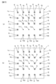
- FIG. 3 is a diagram for explaining a standard arrangement in which via conductors are arranged at all m ⁇ n virtual grid points.
- FIG. 3 is a diagram showing the arrangement positions of a first via conductor and a second via conductor of a multilayer ceramic capacitor in one embodiment.
- FIG. 3 is a diagram showing an equivalent circuit of two multilayer ceramic capacitors connected in parallel to a power supply line.
- FIG. 6 is a diagram illustrating an example of a configuration in which no conductor is arranged.
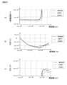
- FIG. 2 is a diagram showing the results of measuring the electrical characteristics of a multilayer ceramic capacitor in one embodiment, a multilayer ceramic capacitor in Comparative Example 1, and a multilayer ceramic capacitor in Comparative Example 2, in which (a) shows the capacitance; (b) ) indicates ESR, and (c) indicates ESL.
- (a) is a perspective view schematically showing the multilayer capacitor described in Patent Document 1
- (b) is a schematic perspective view of the structure when the multilayer capacitor shown in (a) is cut along the XB-XB line.
- FIG. 1 is a plan view schematically showing a multilayer ceramic capacitor 100 in an embodiment of the present invention.
- FIG. 2 is a cross-sectional view schematically showing the structure of the multilayer ceramic capacitor 100 shown in FIG. 1 taken along line II-II.
- FIG. 3 is a cross-sectional view schematically showing the structure of the multilayer ceramic capacitor 100 shown in FIG. 1 taken along line III-III.
- the multilayer ceramic capacitor 100 includes a capacitor body 1 , a first via conductor 5 , a second via conductor 6 , a first external electrode 11 , and a second external electrode 12 .
- the capacitor body 1 has a structure in which a plurality of dielectric layers 2, a plurality of first internal electrodes 3, and a plurality of second internal electrodes 4 are laminated. More specifically, the capacitor body 1 has a structure in which a plurality of first internal electrodes 3 and second internal electrodes 4 are alternately stacked with dielectric layers 2 in between.
- the material of the dielectric layer 2 is arbitrary, and is made of, for example, a ceramic material containing BaTiO 3 , CaTiO 3 , SrTiO 3 , SrZrO 3 , or CaZrO 3 as a main component.
- These main components may contain subcomponents whose content is smaller than that of the main components, such as Mn compounds, Fe compounds, Cr compounds, Co compounds, and Ni compounds.
- the shape of the capacitor body 1 is arbitrary.
- the capacitor main body 1 has a rectangular parallelepiped shape as a whole.
- the shape of a rectangular parallelepiped as a whole is not a perfect rectangular shape, such as a shape with rounded corners and ridges, or a shape with unevenness on the surface of the rectangular parallelepiped, but it has six edges. It is a shape that has a surface and can be regarded as a rectangular parallelepiped as a whole. Therefore, the capacitor body 1 has a first main surface 1a, a second main surface 1b, a first side surface 1c, a second side surface 1d, a third side surface 1e, and a fourth side surface 1f. Equipped with.
- the first main surface 1a and the second main surface 1b of the capacitor body 1 are surfaces facing the stacking direction T of the dielectric layer 2, the first internal electrode 3, and the second internal electrode 4.
- the first main surface 1a and the second main surface 1b have a rectangular shape, more specifically, a square shape.
- the shapes of the first main surface 1a and the second main surface 1b are not limited to rectangles.
- the first side surface 1c to the fourth side surface 1f of the capacitor body 1 are surfaces of the capacitor body 1 other than the first main surface 1a and the second main surface 1b.
- the first side surface 1c to the fourth side surface 1f of the capacitor body 1 are orthogonal to the first main surface 1a and the second main surface 1b, but they do not have to be orthogonal to each other.
- the dimensions of the capacitor body 1 are arbitrary, but for example, the vertical dimension of the rectangle in plan view is 0.3 mm or more and 3.0 mm or less, the horizontal dimension is 0.3 mm or more and 3.0 mm or less, and the lamination direction T is The dimensions can be 50 ⁇ m or more and 200 ⁇ m or less.
- the dimension of the capacitor body 1 in the stacking direction T refers to the thickness of the capacitor body 1.
- the first internal electrode 3 and the second internal electrode 4 may be made of any material, for example, metals such as Ni, Cu, Ag, Pd, Pt, Fe, Ti, Cr, Sn, or Au, or those metals. It is possible to use an alloy containing the like.
- the first internal electrode 3 and the second internal electrode 4 may contain the same ceramic material as the dielectric ceramic contained in the dielectric layer 2 as a common material. In that case, the proportion of the common material contained in the first internal electrode 3 and the second internal electrode 4 is, for example, 20 vol% or less.
- the thickness of the first internal electrode 3 and the second internal electrode 4 is arbitrary, and can be, for example, about 0.3 ⁇ m or more and 1.0 ⁇ m or less.
- the number of layers of the first internal electrode 3 and the second internal electrode 4 is arbitrary, but the total number of both can be, for example, about 10 to 150 layers.
- a plurality of first through holes 3a are formed in the first internal electrode 3 in order to insert a plurality of second via conductors 6, which will be described later.
- a plurality of second through holes 4a are formed in the second internal electrode 4 in order to allow a plurality of first via conductors 5, which will be described later, to be inserted therethrough.
- capacitance is formed by the first internal electrode 3 and the second internal electrode 4 facing each other with the dielectric layer 2 interposed therebetween.
- the first via conductor 5 is provided inside the capacitor body 1 and electrically connected to the plurality of first internal electrodes 3. More specifically, the first via conductor 5 is provided inside the capacitor body 1 in such a manner that it extends in the stacking direction T from the first major surface 1a to the second major surface 1b of the capacitor body 1. .
- the first via conductor 5 passes through a second through hole 4a formed in the second internal electrode 4, and is insulated from the second internal electrode 4.
- the second via conductor 6 is provided inside the capacitor body 1 and electrically connected to the plurality of second internal electrodes 4. More specifically, the second via conductor 6 is provided inside the capacitor body 1 in such a manner that it extends in the stacking direction T from the first major surface 1a to the second major surface 1b of the capacitor body 1. .
- the second via conductor 6 passes through a first through hole 3a formed in the first internal electrode 3, and is insulated from the first internal electrode 3.
- the first via conductor 5 and the second via conductor 6 are each exposed on the second main surface 1b of the capacitor body 1, but they do not need to be exposed.
- the first via conductor 5 and the second via conductor 6 may be made of any material, for example, metals such as Ni, Cu, Ag, Pd, Pt, Fe, Ti, Cr, Sn, or Au, or those metals. It is possible to use an alloy containing the like.
- the shapes of the first via conductor 5 and the second via conductor 6 are arbitrary, they can be, for example, cylindrical. In that case, the diameters of the first via conductor 5 and the second via conductor 6 are, for example, about 30 ⁇ m or more and 150 ⁇ m or less. Further, the distance between the first via conductor 5 and the second via conductor 6 adjacent to each other, more specifically, the distance L1 between the center of the first via conductor 5 and the center of the second via conductor 6 (See FIG. 2) is, for example, about 50 ⁇ m or more and 500 ⁇ m or less.
- the first external electrode 11 is provided on the surface of the capacitor body 1 and is electrically connected to the first via conductor 5.
- the first external electrode 11 is provided only on one of the first main surface 1a and the second main surface 1b facing in the stacking direction T on the surface of the capacitor body 1.
- FIG. 2 shows a configuration in which the first external electrode 11 is provided only on the first main surface 1a of the capacitor body 1.
- the number of first external electrodes 11 is the same as the number of first via conductors 5. As described above, since the first via conductor 5 is electrically connected to the plurality of first internal electrodes 3, the first external electrode 11 is electrically connected to the plurality of first internal electrodes 3. It is connected to the.
- the second external electrode 12 is provided on the surface of the capacitor body 1 and is electrically connected to the second via conductor 6.
- the second external electrode 12 is provided only on one of the first main surface 1a and the second main surface 1b of the capacitor body 1.
- FIG. 2 shows a configuration in which the second external electrode 12 is provided only on the first main surface 1a of the capacitor body 1.
- the number of second external electrodes 12 is the same as the number of second via conductors 6. As described above, since the second via conductor 6 is electrically connected to the plurality of second internal electrodes 4, the second external electrode 12 is electrically connected to the plurality of second internal electrodes 4. It is connected to the.
- the materials of the first external electrode 11 and the second external electrode 12 are arbitrary.
- the first external electrode 11 and the second external electrode 12 are plated electrodes formed by plating.
- Examples of the material constituting the plating electrode include Cu, Ni, and Sn.
- the plating electrode may be composed of a single layer or a plurality of layers.
- the shapes of the first external electrode 11 and the second external electrode 12 when viewed in the stacking direction T are circular.
- the shapes of the first external electrode 11 and the second external electrode 12 when viewed in the stacking direction T are not limited to circular shapes.
- the present invention is characterized by the arrangement positions of the first via conductor 5 and the second via conductor 6.
- the arrangement positions of the first via conductor 5 and the second via conductor 6 of the multilayer ceramic capacitor 100 in this embodiment will be explained below.
- m and n are not limited to 5, and can each take any natural number of 3 or more.
- first via conductor 5 and the second via conductor 6 are not arranged at the following number of virtual lattice points.
- first vias are placed at all virtual grid points T7 to T9, T12 to T14, and T17 to T19 located inside the virtual grid point located at the outermost periphery of the reference arrangement shown in FIG.
- the conductor 5 and the second via conductor 6 are not arranged.
- via conductors including the first via conductor 5 and the second via conductor 6 are arranged only at the outermost virtual lattice points T1 to T6, T10, T11, T15, T16, and T20 to T25.
- first via conductors 5 and second via conductors 6 are alternately arranged in each of the row and column directions of the grid.
- first via conductors 5 and second via conductors 6 are arranged at some virtual lattice points.
- the first via conductor 5 and the second via conductor 6 are arranged at all virtual grid points located inside the virtual grid point located at the outermost periphery of the reference arrangement.
- FIG. 6 shows an equivalent circuit of the multilayer ceramic capacitor 100 and the multilayer ceramic capacitor 110 including a capacitance component (C), a resistance component (R), and an inductance component (L).
- the virtual grid points where the first via conductor 5 and the second via conductor 6 are not arranged are the reference grid points among the virtual grid points located inside the virtual grid points located at the outermost periphery of the reference arrangement.
- the virtual lattice points correspond to via conductors through which a small current flows when a voltage is applied between the first external electrode 11 and the second external electrode 12. That is, when a voltage is applied between the first external electrode 11 and the second external electrode 12 in the standard arrangement, the first via conductor 5 and the second via conductor The magnitude of the current flowing through 6 is different.
- a voltage is applied between the first external electrode 11 and the second external electrode 12 in the standard arrangement among the virtual grid points located inside the virtual grid point located on the outermost periphery of the standard arrangement.
- the first via conductor 5 and the second via conductor 6 are located at a virtual grid point located inside the virtual grid point located at the outermost periphery with respect to the reference arrangement. Since the multilayer ceramic capacitor 100 is not arranged, it is not easily affected by the increase in ESL due to the mounting orientation of the multilayer ceramic capacitor 100 as described above. For example, if the plurality of virtual lattice points at which the first via conductor 5 and the second via conductor 6 are arranged are arranged symmetrically, such as line-symmetrically or point-symmetrically, the multilayer ceramic capacitor 100 This is preferable because it is not affected by an increase in ESL due to the orientation during mounting. In particular, as shown in FIG. This is more preferable because it is not affected by an increase in ESL due to orientation during mounting.
- the difference between the number of first via conductors 5 and the number of second via conductors 6 is one or less. If there is a large difference between the number of first via conductors 5 and the number of second via conductors 6, the distribution of the current flowing through the first via conductor 5 and the distribution of the current flowing through the second via conductor 6 will be different. The bias between them becomes larger and the ESL increases. However, by setting the difference between the number of first via conductors 5 and the number of second via conductors 6 to one or less, the above-described increase in ESL can be suppressed.
- the distribution of the current flowing in the first via conductor 5 and the This is preferable because it is possible to further suppress the deviation between the distribution of the flowing current and the increase in ESL described above.
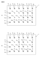
- FIGS. 7(a) and (b) are diagrams each showing another configuration example in which the first via conductor 5 and the second via conductor 6 are not arranged at virtual grid points of (n-2) or less.
- the number of first via conductors 5 and the number of second via conductors 6 are the same.
- the difference between the number of first via conductors 5 and the number of second via conductors 6 is one.
- the first via conductor 5 and the second via conductor 6 may be arranged at virtual lattice points corresponding to the via conductor through which a small current flows when a voltage is applied. Also, it is preferable that the second via conductor 6 is not arranged.
- FIG. 3 is a diagram illustrating a configuration example in which the first via conductor 5 and the second via conductor 6 are not arranged at the following numbers of virtual lattice points.
- the first main surface 1a and the second main surface 1b facing the first main surface 1a each have a rectangular shape.
- the number of first via conductors 5 and the number of second via conductors 6 are the same. Further, in the example shown in FIG. 8(b), since the plurality of virtual lattice points where the first via conductor 5 and the second via conductor 6 are arranged are point symmetrical, the multilayer ceramic capacitor 100 Even if the orientation changes by 180° during mounting, it will not be affected by an increase in ESL.
- FIG. 9 shows a multilayer ceramic capacitor 100 according to the present embodiment, a multilayer ceramic capacitor having the standard arrangement shown in FIG.
- a multilayer ceramic capacitor in which the first via conductor 5 and the second via conductor 6 are not arranged at some of the virtual lattice points T1 to T6, T11, T16, and T21 (hereinafter referred to as the multilayer ceramic capacitor of Comparative Example 2) ) is a diagram showing the results of measuring the electrical characteristics of As shown in FIG. 6, each multilayer ceramic capacitor includes a capacitance component, a resistance component, and an inductance component. 9(a) shows capacitance, FIG. 9(b) shows ESR, and FIG. 9(c) shows ESL.
- the multilayer ceramic capacitor 100 of this embodiment has an increased capacitance compared to the multilayer ceramic capacitor of Comparative Example 1.
- the ESR of the multilayer ceramic capacitor 100 in this embodiment is higher than that of the multilayer ceramic capacitor in Comparative Example 1, but Lower than capacitor ESR.
- the ESL of the multilayer ceramic capacitor 100 in this embodiment is higher than the ESL of the multilayer ceramic capacitor of Comparative Example 1, but lower than the ESL of the multilayer ceramic capacitor of Comparative Example 2.
- the multilayer ceramic capacitor 100 in this embodiment has a larger capacitance than the multilayer ceramic capacitor of Comparative Example 1 in which via conductors are arranged at all virtual lattice points, and The ESR and ESL are lower than the multilayer ceramic capacitor of Comparative Example 2 in which via conductors are not arranged at some of the lattice points.
- the present invention is not limited to the above embodiments, and various applications and modifications can be made within the scope of the present invention.
- the first external electrode 11 and the second external electrode 12 are connected to one main surface of the first main surface 1a and the second main surface 1b facing in the stacking direction T on the surface of the capacitor body 1.
- the description has been made assuming that it is provided only on the surface, it may be provided on both the first main surface 1a and the second main surface 1b.
Landscapes
- Engineering & Computer Science (AREA)
- Power Engineering (AREA)
- Manufacturing & Machinery (AREA)
- Microelectronics & Electronic Packaging (AREA)
- Fixed Capacitors And Capacitor Manufacturing Machines (AREA)
- Ceramic Capacitors (AREA)
Abstract
積層セラミックコンデンサは、複数の誘電体層と、複数の第1の内部電極と、複数の第2の内部電極とが積層されたコンデンサ本体1と、コンデンサ本体1の内部に設けられ、複数の第1の内部電極と電気的に接続されている第1のビア導体5と、コンデンサ本体1の内部に設けられ、複数の第2の内部電極と電気的に接続されている第2のビア導体6と、コンデンサ本体1の表面に設けられ、第1のビア導体5と電気的に接続されている第1の外部電極と、コンデンサ本体1の表面に設けられ、第2のビア導体6と電気的に接続されている第2の外部電極とを備える。コンデンサ本体1を誘電体層、第1の内部電極および第2の内部電極の積層方向に見たときに、m×n(m、nはそれぞれ3以上の自然数)個の仮想格子点を設定し、第1のビア導体5および第2のビア導体6を含むビア導体が全ての仮想格子点に配置された基準配置に対して、最外周に位置する仮想格子点よりも内側に位置する1以上(m-2)×(n-2)以下の数の仮想格子点に第1のビア導体5および第2のビア導体6が配置されていない。
Description
本発明は、積層セラミックコンデンサに関する。
電流の流れるルートを太くする、電流の流れるルートを短くする、極性の異なる電流が発生させる磁界を相互に相殺させるなどして、ESL(等価直列インダクタンス)を小さくした積層コンデンサが知られている。特許文献1には、ESLを小さくした積層コンデンサの一例が開示されている。
特許文献1に開示されている積層コンデンサ200は、図10(a)および(b)に示すように、複数の誘電体層201と、複数の第1の内部電極202と、複数の第2の内部電極203とが積層されたコンデンサ本体210を備えている。コンデンサ本体210は、複数の第1の内部電極202と電気的に接続され、コンデンサ本体210の一方の主面まで延伸している複数の第1のビア導体204と、複数の第2の内部電極203と電気的に接続され、コンデンサ本体210の一方の主面まで延伸している複数の第2のビア導体205とを備えている。コンデンサ本体210の一方の主面には、複数の第1のビア導体204とそれぞれ電気的に接続されている複数の第1の外部電極211と、複数の第2のビア導体205とそれぞれ電気的に接続されている複数の第2の外部電極212が形成されている。複数の第1の外部電極211と複数の第2の外部電極212は、図10(a)に示すように、格子状に配置されており、同様に、複数の第1のビア導体204と複数の第2のビア導体205も格子状に配置されている。
しかしながら、特許文献1に開示されている積層コンデンサ200のように、ビア導体204,205を格子状に複数設けた構成では、第1の内部電極202と第2の内部電極203とが対向する有効領域が低減し、静電容量が低下する。
本発明は、上記課題を解決するものであり、格子状にビア導体が配置された従来の積層セラミックコンデンサと比べて、静電容量を増大させることができる積層セラミックコンデンサを提供することを目的とする。
本発明の積層セラミックコンデンサは、
複数の誘電体層と、複数の第1の内部電極と、複数の第2の内部電極とが積層されたコンデンサ本体と、
前記コンデンサ本体の内部に設けられ、複数の前記第1の内部電極と電気的に接続されている第1のビア導体と、
前記コンデンサ本体の内部に設けられ、複数の前記第2の内部電極と電気的に接続されている第2のビア導体と、
前記コンデンサ本体の表面に設けられ、前記第1のビア導体と電気的に接続されている第1の外部電極と、
前記コンデンサ本体の表面に設けられ、前記第2のビア導体と電気的に接続されている第2の外部電極と、
を備え、
前記コンデンサ本体を前記誘電体層、前記第1の内部電極および前記第2の内部電極の積層方向に見たときに、m×n(m、nはそれぞれ3以上の自然数)個の仮想格子点を設定し、前記第1のビア導体および前記第2のビア導体を含むビア導体が全ての前記仮想格子点に配置された基準配置に対して、最外周に位置する前記仮想格子点よりも内側に位置する1以上(m-2)×(n-2)以下の数の前記仮想格子点に前記第1のビア導体および前記第2のビア導体が配置されていないことを特徴とする。
本発明の積層セラミックコンデンサによれば、m×n個の仮想格子点のうち、最外周に位置する仮想格子点よりも内側に位置する1以上(m-2)×(n-2)以下の数の仮想格子点に第1のビア導体および第2のビア導体が配置されていないので、m×n個の仮想格子点の全てにビア導体が配置されている構成と比べて、静電容量を増大させることができる。
以下に本発明の実施形態を示して、本発明の特徴を具体的に説明する。
図1は、本発明の一実施形態における積層セラミックコンデンサ100を模式的に示す平面図である。図2は、図1に示す積層セラミックコンデンサ100をII-II線に沿って切断したときの構造を模式的に示す断面図である。図3は、図1に示す積層セラミックコンデンサ100をIII-III線に沿って切断したときの構造を模式的に示す断面図である。
積層セラミックコンデンサ100は、コンデンサ本体1と、第1のビア導体5と、第2のビア導体6と、第1の外部電極11と、第2の外部電極12とを備える。
コンデンサ本体1は、複数の誘電体層2と、複数の第1の内部電極3と、複数の第2の内部電極4とが積層された構造を有する。より詳細には、コンデンサ本体1は、誘電体層2を介して第1の内部電極3と第2の内部電極4とが交互に複数積層された構造を有する。
誘電体層2の材質は任意であり、例えば、BaTiO3、CaTiO3、SrTiO3、SrZrO3、または、CaZrO3などを主成分とするセラミック材料からなる。これらの主成分に、Mn化合物、Fe化合物、Cr化合物、Co化合物、Ni化合物などの主成分よりも含有量の少ない副成分が添加されていてもよい。
コンデンサ本体1の形状は任意である。本実施形態では、コンデンサ本体1は、全体として直方体の形状を有する。全体として直方体の形状とは、例えば、直方体の角部や稜線部が丸みを帯びている形状や、直方体の表面に凹凸が存在する形状のように、完全な直方体の形状ではないが、6つの表面を有し、全体として直方体ととらえることができる形状のことである。したがって、コンデンサ本体1は、第1の主面1aと、第2の主面1bと、第1の側面1cと、第2の側面1dと、第3の側面1eと、第4の側面1fとを備える。
コンデンサ本体1の第1の主面1aおよび第2の主面1bは、誘電体層2、第1の内部電極3および第2の内部電極4の積層方向Tに相対する表面である。本実施形態では、第1の主面1aおよび第2の主面1bは、矩形、より詳しくは、正方形の形状を有する。ただし、第1の主面1aおよび第2の主面1bの形状が矩形に限定されることはない。コンデンサ本体1の第1の側面1c~第4の側面1fは、コンデンサ本体1の表面のうち、第1の主面1aおよび第2の主面1b以外の表面である。コンデンサ本体1の第1の側面1c~第4の側面1fは、第1の主面1aおよび第2の主面1bと直交しているが、直交していなくてもよい。
コンデンサ本体1の寸法は任意であるが、例えば、平面視で矩形の縦方向の寸法を0.3mm以上3.0mm以下、横方向の寸法を0.3mm以上3.0mm以下、積層方向Tにおける寸法を50μm以上200μm以下とすることができる。積層方向Tにおけるコンデンサ本体1の寸法とは、コンデンサ本体1の厚みのことである。
第1の内部電極3および第2の内部電極4の材質は任意であり、例えば、Ni、Cu、Ag、Pd、Pt、Fe、Ti、Cr、SnまたはAuなどの金属、またはそれらの金属を含む合金などを用いることが可能である。第1の内部電極3および第2の内部電極4は、共材として、誘電体層2に含まれる誘電体セラミックと同じセラミック材料を含んでいてもよい。その場合、第1の内部電極3および第2の内部電極4に含まれる共材の割合は、例えば、20vol%以下である。
第1の内部電極3および第2の内部電極4の厚さは任意であるが、例えば、0.3μm以上1.0μm以下程度とすることができる。第1の内部電極3および第2の内部電極4の層数は任意であるが、両方を併せて、例えば、10層以上150層以下程度とすることができる。
図2に示すように、第1の内部電極3には、後述する複数の第2のビア導体6を挿通させるために、複数の第1の貫通孔3aが形成されている。第2の内部電極4には、後述する複数の第1のビア導体5を挿通させるために、複数の第2の貫通孔4aが形成されている。
積層セラミックコンデンサ100は、第1の内部電極3と第2の内部電極4とが誘電体層2を介して対向することにより静電容量が形成される。
第1のビア導体5は、コンデンサ本体1の内部に設けられ、複数の第1の内部電極3と電気的に接続されている。より具体的には、第1のビア導体5は、コンデンサ本体1の第1の主面1aから第2の主面1bまで積層方向Tに延伸する態様でコンデンサ本体1の内部に設けられている。第1のビア導体5は、第2の内部電極4に形成されている第2の貫通孔4aを挿通しており、第2の内部電極4とは絶縁されている。
第2のビア導体6は、コンデンサ本体1の内部に設けられ、複数の第2の内部電極4と電気的に接続されている。より具体的には、第2のビア導体6は、コンデンサ本体1の第1の主面1aから第2の主面1bまで積層方向Tに延伸する態様でコンデンサ本体1の内部に設けられている。第2のビア導体6は、第1の内部電極3に形成されている第1の貫通孔3aを挿通しており、第1の内部電極3とは絶縁されている。
なお、図2に示すように、第1のビア導体5および第2のビア導体6はそれぞれ、コンデンサ本体1の第2の主面1bに露出しているが、露出していなくてもよい。
第1のビア導体5および第2のビア導体6の材質は任意であり、例えば、Ni、Cu、Ag、Pd、Pt、Fe、Ti、Cr、SnまたはAuなどの金属、またはそれらの金属を含む合金などを用いることが可能である。
第1のビア導体5および第2のビア導体6の形状は任意であるが、例えば、円柱状とすることができる。その場合の第1のビア導体5および第2のビア導体6の直径は、例えば、30μm以上150μm以下程度である。また、隣り合う第1のビア導体5と第2のビア導体6との間の距離、より詳しくは、第1のビア導体5の中心と第2のビア導体6の中心との間の距離L1(図2参照)は、例えば、50μm以上500μm以下程度である。
第1の外部電極11は、コンデンサ本体1の表面に設けられ、第1のビア導体5と電気的に接続されている。本実施形態では、第1の外部電極11は、コンデンサ本体1の表面のうち、積層方向Tに相対する第1の主面1aおよび第2の主面1bのうちの一方の主面にのみ設けられている。図2では、コンデンサ本体1の第1の主面1aにのみ第1の外部電極11が設けられた構成を示している。第1の外部電極11の数は、第1のビア導体5の数と同じである。上述したように、第1のビア導体5は、複数の第1の内部電極3と電気的に接続されているため、第1の外部電極11は、複数の第1の内部電極3と電気的に接続されている。
第2の外部電極12は、コンデンサ本体1の表面に設けられ、第2のビア導体6と電気的に接続されている。本実施形態では、第2の外部電極12は、コンデンサ本体1の第1の主面1aおよび第2の主面1bのうちの一方の主面にのみ設けられている。図2では、コンデンサ本体1の第1の主面1aにのみ第2の外部電極12が設けられた構成を示している。第2の外部電極12の数は、第2のビア導体6の数と同じである。上述したように、第2のビア導体6は、複数の第2の内部電極4と電気的に接続されているため、第2の外部電極12は、複数の第2の内部電極4と電気的に接続されている。
第1の外部電極11および第2の外部電極12の材質は任意である。本実施形態において、第1の外部電極11および第2の外部電極12は、めっきにより形成されるめっき電極である。めっき電極を構成する材料として、例えば、Cu、Ni、Snなどが挙げられる。めっき電極は、単層で構成されていてもよいし、複数層で構成されていてもよい。
図1に示すように、本実施形態において、積層方向Tに見たときの第1の外部電極11および第2の外部電極12の形状は、円形である。ただし、積層方向Tに見たときの第1の外部電極11および第2の外部電極12の形状が円形に限定されることはない。
本発明は、第1のビア導体5および第2のビア導体6の配置位置に特徴がある。本実施形態における積層セラミックコンデンサ100の第1のビア導体5および第2のビア導体6の配置位置を以下で説明する。
図4に示すように、コンデンサ本体1を積層方向Tに見たときに、m×n(m、nはそれぞれ3以上の自然数)個の仮想格子点T1~Tx(x=m×n)を設定し、第1のビア導体5および第2のビア導体6を含むビア導体7が全ての仮想格子点T1~Txに配置された構成を基準配置とする。m×n個の仮想格子点とは、m行n列で格子状に配置された格子点である。ただし、「仮想格子点」と呼んでいることからも明らかなように、目に見える形でコンデンサ本体1に格子点が設けられているわけではない。図4では、m=5、n=5であり、25個の仮想格子点T1~T25が設定された例を示している。ただし、mとnが5に限定されることはなく、それぞれ3以上の任意の自然数を取り得る。
本実施形態における積層セラミックコンデンサ100では、図5に示すように、図4に示す基準配置に対して、最外周に位置する仮想格子点よりも内側に位置する1以上(m-2)×(n-2)以下の数の仮想格子点に、第1のビア導体5および第2のビア導体6が配置されていない。図5に示す例では、図4に示す基準配置の最外周に位置する仮想格子点よりも内側に位置する全ての仮想格子点T7~T9、T12~T14、T17~T19に、第1のビア導体5および第2のビア導体6が配置されていない。すなわち、最外周の仮想格子点T1~T6、T10、T11、T15、T16、T20~25にのみ、第1のビア導体5および第2のビア導体6を含むビア導体が配置されている。本実施形態では、図5に示すように、格子状の行方向および列方向のそれぞれの方向において、第1のビア導体5と第2のビア導体6が交互に配置されている。
このように、全ての仮想格子点T1~Txにビア導体7を配置する基準配置(図4参照)に対して、一部の仮想格子点に第1のビア導体5および第2のビア導体6を配置しない構成とすることにより、第1の内部電極3と第2の内部電極4とが誘電体層2を介して積層方向Tに対向する有効領域が増えるので、静電容量が増大する。
特に、図5に示すように、基準配置の最外周に位置する仮想格子点よりも内側に位置する全ての仮想格子点に、第1のビア導体5および第2のビア導体6が配置されていない構成とすることにより、より静電容量を増大させることができる。
なお、基準配置の一部の仮想格子点にビア導体を配置しない構成とすることにより、基準配置の積層セラミックコンデンサと比べてESR(等価直列抵抗)とESL(等価直列インダクタンス)は増加する。しかしながら、ESRが増加することによって、図6に示すように、本実施形態における積層セラミックコンデンサ100を、静電容量の異なる他の積層セラミックコンデンサ110と並列に電源ラインに接続した場合に、2つの積層セラミックコンデンサ間で生じる反共振の大きさを低減することができる。なお、図6では、容量成分(C)、抵抗成分(R)およびインダクタンス成分(L)を含む積層セラミックコンデンサ100および積層セラミックコンデンサ110の等価回路を示している。
ここで、第1のビア導体5および第2のビア導体6が配置されていない仮想格子点は、基準配置の最外周に位置する仮想格子点よりも内側に位置する仮想格子点のうち、基準配置において第1の外部電極11と第2の外部電極12との間に電圧が印加されたときに流れる電流が小さいビア導体に対応する仮想格子点であることが好ましい。すなわち、基準配置において第1の外部電極11と第2の外部電極12との間に電圧を印加した際、仮想格子点T1~Txの位置によって、第1のビア導体5および第2のビア導体6に流れる電流の大きさが異なる。電圧印加時に流れる電流が小さいビア導体に対応する仮想格子点に第1のビア導体5および第2のビア導体6を配置しない構成とすることにより、ESLの増加を抑制することができる。
すなわち、基準配置の最外周に位置する仮想格子点よりも内側に位置する仮想格子点のうち、基準配置において第1の外部電極11と第2の外部電極12との間に電圧が印加されたときに流れる電流が小さいビア導体に対応する仮想格子点に、第1のビア導体5および第2のビア導体6を配置しない構成とすることにより、静電容量の増大と、ESLの増加の抑制とを両立させることができる。
ここで、図4に示す基準配置において第1の外部電極11と第2の外部電極12との間に電圧が印加されたときに、仮想格子点T1~T5の位置のビア導体7に流れる電流が大きく、仮想格子点T21~T25の位置のビア導体7に流れる電流が小さい場合に、流れる電流が小さい最外周の仮想格子点T21~T25にビア導体7を配置しない構成とすることが考えられる。ただし、そのような積層セラミックコンデンサを基板等に実装する際、仮想格子点T1~T5側と仮想格子点T21~T25側の向きを逆にして実装してしまうと、ESLの増加を抑制できず、逆にESLを増大させてしまう。
しかしながら、本実施形態における積層セラミックコンデンサ100では、基準配置に対して最外周に位置する仮想格子点よりも内側に位置する仮想格子点に、第1のビア導体5および第2のビア導体6が配置されていないので、上述したような積層セラミックコンデンサ100の実装時の向きによるESLの増加の影響を受けにくい。例えば、第1のビア導体5および第2のビア導体6が配置されている複数の仮想格子点が線対称や点対称のように、対称性のある配置である場合には、積層セラミックコンデンサ100の実装時の向きによるESLの増加の影響を受けることがないので好ましい。特に、図5に示すように、第1のビア導体5および第2のビア導体6が配置されている複数の仮想格子点が点対称の配置となっている場合には、積層セラミックコンデンサ100の実装時の向きによるESLの増加の影響を受けることがないのでより好ましい。
本実施形態において、第1のビア導体5の数と、第2のビア導体6の数との差は、1つ以下である。第1のビア導体5の数と第2のビア導体6の数との差が多いと、第1のビア導体5に流れる電流の分布と、第2のビア導体6に流れる電流の分布との間の偏りが大きくなり、ESLが増加する。しかしながら、第1のビア導体5の数と第2のビア導体6の数との差を1つ以下とすることにより、上述したESLの増加を抑制することができる。特に、第1のビア導体5の数と、第2のビア導体6の数との差が0の構成の場合、第1のビア導体5に流れる電流の分布と、第2のビア導体6に流れる電流の分布との間の偏りをより抑制することができ、上述したESLの増加をより抑制することができるので好ましい。
図7(a)および(b)は、m=n(=5)であって、基準配置に対して、最外周に位置する仮想格子点よりも内側に位置する1以上(m-2)×(n-2)以下の数の仮想格子点に、第1のビア導体5および第2のビア導体6が配置されていない別の構成例をそれぞれ示す図である。図7(a)に示す例では、第1のビア導体5の数と第2のビア導体6の数は同じである。図7(b)に示す例では、第1のビア導体5の数と第2のビア導体6の数の差は1つである。図7(a)および図7(b)に示すように、基準配置に対して、最外周に位置する仮想格子点よりも内側に位置する仮想格子点のうち、任意の仮想格子点に第1のビア導体5および第2のビア導体6が配置されない構成とすることができるが、上述したように、電圧印加時に流れる電流が小さいビア導体に対応する仮想格子点に、第1のビア導体5および第2のビア導体6を配置しない構成とすることが好ましい。
図8(a)および(b)は、m=nではなく、基準配置に対して、最外周に位置する仮想格子点よりも内側に位置する1以上(m-2)×(n-2)以下の数の仮想格子点に、第1のビア導体5および第2のビア導体6が配置されていない構成例をそれぞれ示す図である。図8では、m=4、n=6とした例を示しているが、上述したように、mおよびnは任意の自然数を取り得る。図8(a)および(b)に示すように、第1の主面1a、および、第1の主面1aと相対する第2の主面1bはそれぞれ、長方形の形状を有する。
図8(a)および図8(b)に示す例では、第1のビア導体5の数と第2のビア導体6の数は同じである。また、図8(b)に示す例では、第1のビア導体5および第2のビア導体6が配置されている複数の仮想格子点が点対称の配置となっているため、積層セラミックコンデンサ100の実装時に向きが180°変わっても、ESLの増加の影響を受けることがない。
図9は、本実施形態における積層セラミックコンデンサ100、図4に示す基準配置の積層セラミックコンデンサ(以下、比較例1の積層セラミックコンデンサと呼ぶ)、および、図4に示す基準配置に対して最外周の一部の仮想格子点T1~T6、T11、T16およびT21に第1のビア導体5および第2のビア導体6が配置されていない積層セラミックコンデンサ(以下、比較例2の積層セラミックコンデンサと呼ぶ)の電気特性を測定した結果を示す図である。それぞれの積層セラミックコンデンサは、図6に示すように、容量成分、抵抗成分およびインダクタンス成分を含むものとする。図9(a)は、静電容量を、図9(b)は、ESRを、図9(c)は、ESLを示す。
図9(a)に示すように、本実施形態における積層セラミックコンデンサ100は、比較例1の積層セラミックコンデンサと比べて、静電容量が増加している。一方、図9(b)および図9(c)に示すように、本実施形態における積層セラミックコンデンサ100のESRは、比較例1の積層セラミックコンデンサのESRよりも高いが、比較例2の積層セラミックコンデンサのESRよりも低い。また、本実施形態における積層セラミックコンデンサ100のESLは、比較例1の積層セラミックコンデンサのESLよりも高いが、比較例2の積層セラミックコンデンサのESLよりも低い。
すなわち、本実施形態における積層セラミックコンデンサ100は、全ての仮想格子点にビア導体が配置された比較例1の積層セラミックコンデンサよりも静電容量が大きく、かつ、標準配置に対して最外周の仮想格子点の一部にビア導体が配置されていない比較例2の積層セラミックコンデンサよりも、ESRおよびESLが低い。
本発明は、上記実施形態に限定されるものではなく、本発明の範囲内において、種々の応用、変形を加えることが可能である。例えば、第1の外部電極11および第2の外部電極12は、コンデンサ本体1の表面のうち、積層方向Tに相対する第1の主面1aおよび第2の主面1bのうちの一方の主面にのみ設けられているものとして説明したが、第1の主面1aおよび第2の主面1bの両方に設けられていてもよい。
1 コンデンサ本体
2 誘電体層
3 第1の内部電極
4 第2の内部電極
5 第1のビア導体
6 第2のビア導体
7 ビア導体
11 第1の外部電極
12 第2の外部電極
100 積層セラミックコンデンサ
T1~T25 仮想格子点
2 誘電体層
3 第1の内部電極
4 第2の内部電極
5 第1のビア導体
6 第2のビア導体
7 ビア導体
11 第1の外部電極
12 第2の外部電極
100 積層セラミックコンデンサ
T1~T25 仮想格子点
Claims (6)
- 複数の誘電体層と、複数の第1の内部電極と、複数の第2の内部電極とが積層されたコンデンサ本体と、
前記コンデンサ本体の内部に設けられ、複数の前記第1の内部電極と電気的に接続されている第1のビア導体と、
前記コンデンサ本体の内部に設けられ、複数の前記第2の内部電極と電気的に接続されている第2のビア導体と、
前記コンデンサ本体の表面に設けられ、前記第1のビア導体と電気的に接続されている第1の外部電極と、
前記コンデンサ本体の表面に設けられ、前記第2のビア導体と電気的に接続されている第2の外部電極と、
を備え、
前記コンデンサ本体を前記誘電体層、前記第1の内部電極および前記第2の内部電極の積層方向に見たときに、m×n(m、nはそれぞれ3以上の自然数)個の仮想格子点を設定し、前記第1のビア導体および前記第2のビア導体を含むビア導体が全ての前記仮想格子点に配置された基準配置に対して、最外周に位置する前記仮想格子点よりも内側に位置する1以上(m-2)×(n-2)以下の数の前記仮想格子点に前記第1のビア導体および前記第2のビア導体が配置されていないことを特徴とする積層セラミックコンデンサ。 - 前記第1のビア導体の数と、前記第2のビア導体の数との差は、1つ以下であることを特徴とする請求項1に記載の積層セラミックコンデンサ。
- 前記第1のビア導体および前記第2のビア導体が配置されていない前記仮想格子点は、前記基準配置の前記最外周に位置する前記仮想格子点よりも内側に位置する前記仮想格子点のうち、前記基準配置において前記第1の外部電極と前記第2の外部電極との間に電圧が印加されたときに流れる電流が小さい前記ビア導体に対応する前記仮想格子点であることを特徴とする請求項1または2に記載の積層セラミックコンデンサ。
- 前記第1のビア導体および前記第2のビア導体は、前記基準配置の前記最外周に位置する前記仮想格子点よりも内側に位置する全ての前記仮想格子点に配置されていないことを特徴とする請求項1または2に記載の積層セラミックコンデンサ。
- 前記第1のビア導体および前記第2のビア導体が配置されている複数の前記仮想格子点は、対称性のある配置であることを特徴とする請求項1~4のいずれか一項に記載の積層セラミックコンデンサ。
- 前記第1の外部電極および前記第2の外部電極は、前記コンデンサ本体の表面のうち、前記積層方向に相対する第1の主面および第2の主面のうちの一方の主面にのみ設けられていることを特徴とする請求項1~5のいずれか一項に記載の積層セラミックコンデンサ。
Applications Claiming Priority (2)
| Application Number | Priority Date | Filing Date | Title |
|---|---|---|---|
| JP2022-043492 | 2022-03-18 | ||
| JP2022043492 | 2022-03-18 |
Publications (1)
| Publication Number | Publication Date |
|---|---|
| WO2023176538A1 true WO2023176538A1 (ja) | 2023-09-21 |
Family
ID=88023037
Family Applications (1)
| Application Number | Title | Priority Date | Filing Date |
|---|---|---|---|
| PCT/JP2023/008255 WO2023176538A1 (ja) | 2022-03-18 | 2023-03-06 | 積層セラミックコンデンサ |
Country Status (1)
| Country | Link |
|---|---|
| WO (1) | WO2023176538A1 (ja) |
Citations (1)
| Publication number | Priority date | Publication date | Assignee | Title |
|---|---|---|---|---|
| JPH11204372A (ja) * | 1997-11-14 | 1999-07-30 | Murata Mfg Co Ltd | 積層コンデンサ |
-
2023
- 2023-03-06 WO PCT/JP2023/008255 patent/WO2023176538A1/ja unknown
Patent Citations (1)
| Publication number | Priority date | Publication date | Assignee | Title |
|---|---|---|---|---|
| JPH11204372A (ja) * | 1997-11-14 | 1999-07-30 | Murata Mfg Co Ltd | 積層コンデンサ |
Similar Documents
| Publication | Publication Date | Title |
|---|---|---|
| TW516052B (en) | Multilayer electronic device | |
| JP4230469B2 (ja) | 積層コンデンサ | |
| JP4374041B2 (ja) | 積層コンデンサ | |
| US7436648B2 (en) | Multilayer capacitor and mounted structure thereof | |
| JP4166235B2 (ja) | 積層コンデンサ | |
| JP2006286731A (ja) | 積層コンデンサ | |
| KR101309499B1 (ko) | 관통형 적층 콘덴서 | |
| JP4539715B2 (ja) | 積層コンデンサアレイ | |
| JP5870674B2 (ja) | 積層コンデンサアレイ | |
| KR20100036982A (ko) | 적층 콘덴서 | |
| JP6111768B2 (ja) | 貫通型コンデンサ | |
| JP4720840B2 (ja) | 積層コンデンサの実装構造 | |
| WO2023176538A1 (ja) | 積層セラミックコンデンサ | |
| JP5861531B2 (ja) | 積層コンデンサ | |
| JP4539713B2 (ja) | 積層コンデンサアレイ | |
| JP2021015962A (ja) | 積層型キャパシタ及びその実装基板 | |
| KR20140143341A (ko) | 적층 세라믹 커패시터 및 그 실장 기판 | |
| JP5093044B2 (ja) | 積層コンデンサ | |
| JP6459717B2 (ja) | 積層セラミックコンデンサ | |
| JP2010087260A (ja) | 積層コンデンサ | |
| JP4952779B2 (ja) | 積層コンデンサアレイ | |
| US20230360854A1 (en) | Multilayer ceramic capacitor | |
| JP2018006736A (ja) | 電子部品 | |
| WO2022034797A1 (ja) | 多端子積層コンデンサ | |
| JP2012104784A (ja) | 貫通コンデンサ |
Legal Events
| Date | Code | Title | Description |
|---|---|---|---|
| 121 | Ep: the epo has been informed by wipo that ep was designated in this application |
Ref document number: 23770494 Country of ref document: EP Kind code of ref document: A1 |