WO2022034797A1 - 多端子積層コンデンサ - Google Patents
多端子積層コンデンサ Download PDFInfo
- Publication number
- WO2022034797A1 WO2022034797A1 PCT/JP2021/027872 JP2021027872W WO2022034797A1 WO 2022034797 A1 WO2022034797 A1 WO 2022034797A1 JP 2021027872 W JP2021027872 W JP 2021027872W WO 2022034797 A1 WO2022034797 A1 WO 2022034797A1
- Authority
- WO
- WIPO (PCT)
- Prior art keywords
- internal electrode
- terminal
- slit
- vias
- external terminals
- Prior art date
Links
Images


Classifications
-
- H—ELECTRICITY
- H01—ELECTRIC ELEMENTS
- H01G—CAPACITORS; CAPACITORS, RECTIFIERS, DETECTORS, SWITCHING DEVICES OR LIGHT-SENSITIVE DEVICES, OF THE ELECTROLYTIC TYPE
- H01G4/00—Fixed capacitors; Processes of their manufacture
- H01G4/002—Details
- H01G4/228—Terminals
- H01G4/232—Terminals electrically connecting two or more layers of a stacked or rolled capacitor
-
- H—ELECTRICITY
- H01—ELECTRIC ELEMENTS
- H01G—CAPACITORS; CAPACITORS, RECTIFIERS, DETECTORS, SWITCHING DEVICES OR LIGHT-SENSITIVE DEVICES, OF THE ELECTROLYTIC TYPE
- H01G4/00—Fixed capacitors; Processes of their manufacture
- H01G4/002—Details
- H01G4/005—Electrodes
- H01G4/012—Form of non-self-supporting electrodes
-
- H—ELECTRICITY
- H01—ELECTRIC ELEMENTS
- H01G—CAPACITORS; CAPACITORS, RECTIFIERS, DETECTORS, SWITCHING DEVICES OR LIGHT-SENSITIVE DEVICES, OF THE ELECTROLYTIC TYPE
- H01G4/00—Fixed capacitors; Processes of their manufacture
- H01G4/30—Stacked capacitors
-
- H—ELECTRICITY
- H01—ELECTRIC ELEMENTS
- H01G—CAPACITORS; CAPACITORS, RECTIFIERS, DETECTORS, SWITCHING DEVICES OR LIGHT-SENSITIVE DEVICES, OF THE ELECTROLYTIC TYPE
- H01G4/00—Fixed capacitors; Processes of their manufacture
- H01G4/38—Multiple capacitors, i.e. structural combinations of fixed capacitors
- H01G4/385—Single unit multiple capacitors, e.g. dual capacitor in one coil
-
- H—ELECTRICITY
- H01—ELECTRIC ELEMENTS
- H01G—CAPACITORS; CAPACITORS, RECTIFIERS, DETECTORS, SWITCHING DEVICES OR LIGHT-SENSITIVE DEVICES, OF THE ELECTROLYTIC TYPE
- H01G4/00—Fixed capacitors; Processes of their manufacture
- H01G4/002—Details
- H01G4/018—Dielectrics
- H01G4/06—Solid dielectrics
- H01G4/08—Inorganic dielectrics
- H01G4/12—Ceramic dielectrics
Definitions
- the present invention relates to a multi-terminal multilayer capacitor.
- Patent Document 1 a capacitor main body, a first internal electrode and a second internal electrode alternately arranged so as to face each other with each layer of the laminated dielectric layer sandwiched between them, and a first surface formed on one or more of the upper and lower surfaces of the main body. It is composed of a first external terminal, a second external terminal, and a first conductive via hole and a second conductive via hole formed in the stacking direction of the main body and connected to the first external terminal and the second external terminal, respectively. Stacked capacitor arrays are disclosed. In particular, in this laminated capacitor array, in order to reduce ESL, the magnetic fields induced by the currents flowing through the internal electrodes connected to the first conductive via holes and the second conductive via holes are mutually canceled. (Alternate arrangement).
- Patent Document 2 in order to reduce ESL, the internal electrode and the external terminal electrode are connected via the via hole conductor, and the via hole conductor penetrates through the internal electrode electrically insulated from the via hole conductor.
- a laminated capacitor in which an island-shaped punching portion is formed in a portion to be formed is disclosed.
- a plurality of island-shaped punching portions are connected to each other, and a punching connecting portion is formed so as to connect the outer side portions of the internal electrodes and the island-shaped punching portions. That is, a punching connection portion is formed so as to divide (divide) the internal electrodes into a plurality of regions isolated from each other.
- the internal electrodes are divided (divided) into a plurality of regions by the unplugged connecting portion, so that the characteristics such as capacitance and ESR (equivalent series resistance) may deteriorate. , And the mechanical strength of the element may decrease. In particular, these problems may become noticeable when the vias are arranged at a narrow pitch.
- the present invention has been made to solve the above-mentioned problems, and it is possible to suppress a decrease in capacitance (effective value) while maintaining a low ESL in a high frequency region, and to secure mechanical strength of an element. It is an object of the present invention to provide a possible multi-terminal multilayer capacitor.
- the multi-terminal laminated capacitor according to the present invention is arranged inside a first internal electrode and a second internal electrode alternately laminated via a dielectric layer, and inside the first internal electrode and the second internal electrode in a plan view.
- a plurality of first external terminals connected to each of the plurality of first vias and a plurality of second external terminals connected to each of the plurality of second vias, and the first via is a first via a first slit.
- the plurality of regions are arranged so as to be electrically connected, and the second via is divided into a plurality of regions by a second slit.
- the plurality of regions are arranged so as to be electrically connected to each other.
- the first via when the first internal electrode is divided into a plurality of regions by the first slit, the first via is arranged so as to electrically connect the plurality of regions.
- the second internal electrode is divided into a plurality of regions by the two slits, the second via is arranged so as to electrically connect the plurality of regions. Therefore, it is avoided that the first and second internal electrodes are divided (divided) into a plurality of regions isolated from each other. Then, when a voltage is applied to the first and second external terminals, a common voltage is applied to the first and second internal electrodes, respectively, through the conduction connection with the first and second vias.
- the capacity can be increased as compared with the case where the internal electrode is electrically divided (divided). Further, since the multi-terminal laminated capacitor is composed of two conductors as a whole, it is possible to suppress the occurrence of an unnecessary resonance mode at high frequencies.
- a first slit is formed so as to extend between the first insulating portion formed around the second via penetrating the first internal electrode and insulating the second via and the first internal electrode, and the first via.
- a second slit is formed so as to extend between the second insulating portion formed around the first via penetrating the second internal electrode and insulating the first via and the second internal electrode, and the second via.
- the voltage drop seen in the axial direction of the first and second vias becomes small, and the decrease in capacitance in the high frequency region is alleviated (that is, the frequency characteristic of the capacitance is flattened).
- the effect of reducing ESR and ESL can be obtained.
- first vias are arranged inside the first internal electrode and the second internal electrode in a plan view
- second vias are arranged inside the first internal electrode and the second internal electrode in a plan view.
- the first and second vias are not arranged on the outer edges of the first and second internal electrodes. Therefore, the outer edge (outer circumference) of the first and second internal electrodes is not divided by the first and second slits. Therefore, the mechanical strength of the element can be ensured.
- FIG. 3 is a cross-sectional view taken along the line II-II of FIG.
- FIG. 3 is a cross-sectional view taken along the line III-III of FIG.
- It is a figure which shows the equivalent circuit of the multi-terminal laminated capacitor which concerns on 1st Embodiment.
- It is an exploded perspective view which shows the internal structure of the multi-terminal laminated capacitor which concerns on 1st Embodiment.
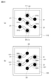
- It is a top view which shows the structure of (a) 1st internal electrode, (b) the 2nd internal electrode which comprises the multi-terminal laminated capacitor which concerns on 1st Embodiment.
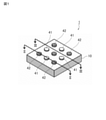
- FIG. 1 is a perspective view showing the configuration of the multi-terminal laminated capacitor 1.
- FIG. 2 is a cross-sectional view taken along the line II-II of FIG.
- FIG. 3 is a cross-sectional view taken along the line III-III of FIG.
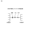
- FIG. 4 is a diagram showing an equivalent circuit of the multi-terminal multilayer capacitor 1.
- minute L (inductance) and R (resistance) are parasitic on the first and second external terminals 41 and 42, but in the equivalent circuit shown in FIG. 4, these parasitic L and R are ESL. And ESR, and the direct display was omitted.
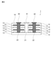
- FIG. 5 is an exploded perspective view showing the internal structure of the multi-terminal laminated capacitor 1.
- FIG. 6 is a plan view showing the configurations of (a) the first internal electrode 11 and (b) the second internal electrode 12 constituting the multi-terminal laminated capacitor 1.
- the multi-terminal laminated capacitor 1 includes, for example, a laminated body 10 formed in a rectangular parallelepiped shape, nine external terminals 41 and 42 formed on the top surface (upper surface) of the laminated body 10, and more specifically, four first terminals. It includes one external terminal 41 and five second external terminals 42.
- the laminated body 10 is configured by alternately laminating the first internal electrode 11 and the second internal electrode 12 so as to face each other via a plurality of dielectric layers (insulator layers) 13 formed in a rectangular shape.
- the dielectric layer 13 is formed of, for example, a dielectric ceramic containing Badio 3, CaTIO 3 , SrTiO 3 , CaZrO 3 , and the like as main components.
- auxiliary components such as Mn compound, Fe compound, Cr compound, Co compound, and Ni compound may be added to these main components.
- the first internal electrode 11 and the second internal electrode 12 are formed, for example, in the form of a rectangular thin film.
- Each of the first internal electrode 11 and the second internal electrode 12 is formed of, for example, Ni, Cu, Ag, Pd, Ag—Pd alloy, Au, or the like.
- the laminate 10 is arranged inside the first internal electrode 11 and the second internal electrode 12 (that is, without touching the outer edge) in a plan view, and is electrically connected (conducted) to the first internal electrode 11.
- a plurality of (four in this embodiment) first vias 21 are formed so as to be insulated from the second internal electrode 12 and penetrate the laminated body 10 in the laminated direction (thickness direction).
- the laminate 10 is arranged inside the first internal electrode 11 and the second internal electrode 12 (that is, without touching the outer edge) in a plan view, and is electrically connected to the second internal electrode 12 (that is, without touching the outer edge).
- a plurality of (five in this embodiment) second vias 22 are formed so as to be conductive and insulated from the first internal electrode 11 and penetrate the laminated body 10 in the laminating direction (thickness direction).
- a plurality of (4) first external terminals 41 are connected to the ends of each of the plurality (4) first vias 21.
- a plurality of (five) second external terminals 42 are connected to the ends of each of the plurality (five) second vias 22.
- the first external terminal 41 and the second external terminal 42 are formed of, for example, a conductive material containing silver as a main component.
- the first external terminal 41 (first via 21) and the second external terminal 42 (second via 22) are arranged alternately and in a matrix shape in a plan view.
- the configuration was set.
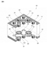
- the first internal electrode 11 has an annular first insulating portion (opening) formed around the second via 22 penetrating the first internal electrode 11 and insulating the second via 22 and the first internal electrode 11. 111 is formed. Further, a linear first slit (gap) 31 is formed so as to extend between the first insulating portion 111 and the first via 21.
- the second internal electrode 12 has an annular second insulating portion (which is formed around the first via 21 penetrating the second internal electrode 12 and insulates the first via 21 and the second internal electrode 12.
- the opening) 121 is formed.
- a linear second slit (gap) 32 is formed so as to extend between the second insulating portion 121 and the second via 22.
- the first slit 31 and the second slit 32 are formed in a grid pattern (a grid pattern) of 3 rows and 3 columns.
- the shapes of the first and second slits 31 and 32 are not limited to 3 rows and 3 columns, and can be arbitrarily set according to requirements and the like (the same applies hereinafter). Further, in the present embodiment, the first slit 31 and the second slit 32 are formed so as to overlap (match) in a plan view.
- the first internal electrode 11 when the first internal electrode 11 is divided into a plurality of regions (five regions in the present embodiment) by the first slit 31, the first via 21 electrically connects (conducts) the plurality of regions. ). Therefore, the first internal electrode 11 is a single internal electrode having a common potential.
- the second internal electrode 12 when the second internal electrode 12 is divided into a plurality of regions (five regions in the present embodiment) by the second slit 32, the second via 22 electrically connects (conducts) the plurality of regions. ). Therefore, the second internal electrode 12 becomes a single internal electrode having a common potential.
- the first internal electrode 11 when the first internal electrode 11 is divided into a plurality (five) regions by the first slit 31, the plurality of regions are electrically divided.
- the first via 21 is arranged so as to be connected (conducting) and the second internal electrode 12 is divided into a plurality (five) regions by the second slit 32, the plurality of regions are electrically connected.
- the second via 22 is arranged so as to be (conducting). Therefore, it is avoided that the first and second internal electrodes 11 and 12 are divided (divided) into a plurality of regions isolated from each other.
- the first and second internal electrodes 11 and 12 are common to the first and second internal electrodes 11 and 12, respectively, through conduction connection with the first and second vias 21 and 22. Voltage is applied. Therefore, the capacity can be increased as compared with the case where the internal electrode is electrically divided (divided). Further, since the multi-terminal laminated capacitor 1 is composed of two conductors as a whole, it is possible to suppress the generation of unnecessary resonance modes at high frequencies.
- the first slit 31 is formed so as to extend between the first insulating portion 111 that insulates the second via 22 and the first internal electrode 11 and the first via 21.
- a second slit 32 is formed so as to extend between the second insulating portion 121 that insulates the 1 via 21 and the second internal electrode 12 and the second via 22. Therefore, when the first and second vias 21 and 22 are viewed in a cross section including the center thereof and the first and second slits 31 and 32, the conductors along the axial direction of the first and second vias 21 and 22. The surface path is shortened. As a result, the impedance along the axial direction of the first and second vias 21 and 22 is reduced.
- the voltage drop seen in the axial direction of the first and second vias 21 and 22 becomes small, and the decrease in capacitance in the high frequency region is alleviated (that is, the frequency characteristic of the capacitance is flattened).
- the effect of reducing ESR and ESL can be obtained.
- the plurality of first vias 21 and the plurality of second vias 22 are inside the first internal electrode 11 and the second internal electrode 12 (that is, without touching the outer edge) in a plan view. ) Be placed. That is, the first and second vias 21 and 22 are not arranged on the outer edges of the first and second internal electrodes 11 and 12. Therefore, the outer edges (outer circumferences) of the first and second internal electrodes 11 and 12 are not divided by the first and second slits 31 and 32. Therefore, the mechanical strength of the element can be ensured, and the flatness of the element can be ensured.
- FIG. 7 shows (a) impedance characteristics and (b) ESR characteristics of the multi-terminal multilayer capacitor 1 and the comparative example according to the present embodiment.
- FIG. 7A shows the impedance characteristics (simulation results) of the multi-terminal laminated capacitor 1 and the comparative example
- FIG. 7B shows the ESR characteristics (simulation results) of the multi-terminal laminated capacitor 1 and the comparative example.
- the horizontal axis of the graph of FIG. 7A is frequency (Hz), and the vertical axis is impedance ( ⁇ ). Further, the horizontal axis of the graph of (b) is frequency (Hz), and the vertical axis is ESR ( ⁇ ).
- FIG. 7A it was confirmed that the impedance (particularly, the impedance near 100 MHz) is lower than that of the comparative example according to the multi-terminal multilayer capacitor 1. Further, as shown in FIG. 7B, it was confirmed that the ESR was lowered according to the multi-terminal laminated capacitor 1 as compared with the comparative example.
- FIG. 8 shows (a) capacitance characteristics and (b) ESL characteristics of the multi-terminal laminated capacitor 1 and the comparative example.
- FIG. 8A shows the capacitance characteristics (simulation results) of the multi-terminal laminated capacitor 1 and the comparative example
- FIG. 8B shows the ESL characteristics (simulation results) of the multi-terminal laminated capacitor 1 and the comparative example.
- the horizontal axis of the graph of FIG. 8A is frequency (Hz), and the vertical axis is capacitance (F).
- the horizontal axis of the graph of (b) is frequency (Hz)
- the vertical axis is ESL (H).
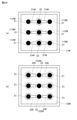
- the first slit 31 and the second slit 32 are formed in a grid pattern, but as shown in FIG. 9, the first slit 31B and the second slit 32 are formed.
- the second slit 32B may be formed into three linear shapes extending parallel to the contours of the first internal electrode 11B and the second internal electrode 12B.
- FIG. 9 is a plan view showing the configurations of (a) the first internal electrode 11B and (b) the second internal electrode 12B constituting the multi-terminal laminated capacitor 1B according to the second embodiment.
- the first slit 31B and the second slit 32B are formed so as to overlap (match) in a plan view.
- the first and second internal electrodes 11B and 12B do not have an electrically divided (divided) region. Since other configurations are the same as or similar to those of the multi-terminal multilayer capacitor 1 according to the first embodiment described above, detailed description thereof will be omitted here.
- FIG. 10 shows (a) impedance characteristics and (b) ESR characteristics of the multi-terminal multilayer capacitor 1B and the comparative example according to the present embodiment.
- FIG. 10A shows the impedance characteristics (simulation results) of the multi-terminal laminated capacitor 1B and the comparative example
- FIG. 10B shows the ESR characteristics (simulation results) of the multi-terminal laminated capacitor 1B and the comparative example.
- the horizontal axis of the graph of FIG. 10A is frequency (Hz), and the vertical axis is impedance ( ⁇ ).
- the horizontal axis of the graph of (b) is frequency (Hz), and the vertical axis is ESR ( ⁇ ).
- the impedance (particularly, the impedance near 100 MHz) is lower than that of the comparative example according to the multi-terminal multilayer capacitor 1B. Further, as shown in FIG. 10B, it was confirmed that the ESR was lowered as compared with the comparative example according to the multi-terminal laminated capacitor 1B. That is, it was confirmed that the multi-terminal laminated capacitor 1B according to the second embodiment can also exert the same effect as the multi-terminal laminated capacitor 1 according to the first embodiment described above.
- FIG. 11 shows (a) capacitance characteristics and (b) ESL characteristics of the multi-terminal laminated capacitor 1B and the comparative example.
- FIG. 11A shows the capacitance characteristics (simulation results) of the multi-terminal laminated capacitor 1B and the comparative example
- FIG. 11B shows the ESL characteristics (simulation results) of the multi-terminal laminated capacitor 1B and the comparative example.
- the horizontal axis of the graph of FIG. 11A is frequency (Hz), and the vertical axis is capacitance (F).
- the horizontal axis of the graph of (b) is frequency (Hz)
- the vertical axis is ESL (H).
- FIG. 11A in the comparative example, a decrease in capacitance was observed in the high frequency region (particularly in the region of 10 MHz or more), but according to the multi-terminal multilayer capacitor 1B, the high frequency region (particularly 10 MHz) was observed. It was confirmed that the capacity did not decrease even in the above area). Further, as shown in FIG. 11B, it was confirmed that the ESL can be maintained low according to the multi-terminal laminated capacitor 1B. That is, it was confirmed that the multi-terminal laminated capacitor 1B according to the second embodiment can also exert the same effect as the multi-terminal laminated capacitor 1 according to the first embodiment described above.
- FIG. 12 is a plan view showing the configurations of (a) the first internal electrode 11B and (b) the second internal electrode 12C constituting the multi-terminal laminated capacitor 1C according to the third embodiment.
- the first slit 31B and the second slit 32C are configured to be orthogonal to each other. Therefore, in the present embodiment, the first slit 31B and the second slit 32C do not overlap (that is, do not match) in a plan view. Further, in this case, the first and second internal electrodes 11B and 12C do not have an electrically divided (divided) region. Since other configurations are the same as or similar to those of the multi-terminal multilayer capacitor 1B according to the second embodiment described above, detailed description thereof will be omitted here.
- the magnetic fields entering and exiting the first slit 31B and the second slit 32C are linear. Although it is not distributed (that is, it deviates from the optimum conditions), it is possible to obtain almost the same effect as the multi-terminal laminated capacitor 1B according to the second embodiment described above.
- the widths of the first slit 31 and the second slit 32 are constant, but as shown in FIG. 13, the first via 21 of the first slit 31D and the first via 21
- the contact portion (connection portion) of the above may be formed in a tapered shape that narrows toward the contact portion.
- the contact portion (connecting portion) of the second slit 32D with the second via 22 may be formed in a tapered shape that narrows toward the contact portion.
- FIG. 13 is a plan view showing the configurations of (a) the first internal electrode 11D and (b) the second internal electrode 12D constituting the multi-terminal laminated capacitor 1D according to the fourth embodiment. Since other configurations are the same as or similar to those of the multi-terminal multilayer capacitor 1 according to the first embodiment described above, detailed description thereof will be omitted here.
- the first and second slits 31D and 32D in a tapered shape, conduction connection between the first and second internal electrodes 11D and 12D and the first and second vias 21 and 22 can be established. It can be achieved reliably, and the influence of misalignment (variation) can be reduced. Further, when the element is fired in the manufacturing process, the element shrinks similarly, but by forming the first and second slits 31D and 32D in a tapered shape, the shapes of the first and second slits 31D and 32D are formed even after firing. Can be well secured (maintained).
- a land pattern may be provided at the connection portion between the first and second vias 21 and 22 and the first and second slits 31 and 32 with respect to the multi-terminal laminated capacitor 1 according to the first embodiment described above.
- connection portion of the first internal electrode 11E with the first via 21 is formed in an annular shape. That is, an annular first land pattern 112E is formed around the first via 21 penetrating the first internal electrode 11E.
- connection portion of the second internal electrode 12E with the second via 22 is formed in an annular shape. That is, an annular second land pattern 122E is formed around the second via 22 penetrating the second internal electrode 12E.
- FIG. 14 is a plan view showing the configurations of (a) the first internal electrode 11E and (b) the second internal electrode 12E constituting the multi-terminal laminated capacitor 1E according to the fifth embodiment.
- the first slit 31E is formed so as to connect the first insulating portion 111 and the first land pattern 112E (first via 21).
- the second slit 32E is formed so as to connect the second insulating portion 121 and the second land pattern 122E (second via 22).
- the diameters of the first and second land patterns 112E and 122E are larger than the widths of the first and second slits 31E and 32E, and larger than the diameters of the first and second vias 21 and 22. Since other configurations are the same as or similar to those of the multi-terminal multilayer capacitor 1 according to the first embodiment described above, detailed description thereof will be omitted here.
- the conduction connection between the first and second internal electrodes 11E and 12E and the first and second vias 21 and 22 is surely achieved. It is possible to reduce the influence of misalignment and the like (variation).
- first external terminal 41 first via 21
- second external terminal 42 second via 22
- first external terminal 41 first via 21
- second external terminal 42 second via 22
- first external terminal 41 first via 21
- second external terminal 42 second via 22
- FIG. 15 is a plan view showing the configurations of (a) the first internal electrode 11F and (b) the second internal electrode 12F constituting the multi-terminal laminated capacitor 1F according to the sixth embodiment. Further, FIG. 16 is an exploded perspective view showing the internal structure of the multi-terminal laminated capacitor 1F.
- the first and second external terminals 41 and 42 are aligned with the same polarity.
- the land pattern of the mounting board for example, mounting on a linear line such as a microstrip line or a coplanar line can be performed. It will be easy (possible).
- the ground signal ground (GSG) is arranged, and a through-type capacitor is connected to form a single chip. This facilitates handling at the time of mounting.
- FIG. 17 shows (a) impedance characteristics and (b) ESR characteristics of the multi-terminal multilayer capacitor 1F and the comparative example according to the present embodiment.
- FIG. 17A shows the impedance characteristics (simulation results) of the multi-terminal laminated capacitor 1F and the comparative example
- FIG. 17B shows the ESR characteristics (simulation results) of the multi-terminal laminated capacitor 1F and the comparative example.
- the horizontal axis of the graph of FIG. 17A is frequency (Hz), and the vertical axis is impedance ( ⁇ ). Further, the horizontal axis of the graph of (b) is frequency (Hz), and the vertical axis is ESR ( ⁇ ).
- the impedance (particularly, the impedance of 100 MHz or less) is lower than that of the comparative example according to the multi-terminal laminated capacitor 1F.
- FIG. 17B it was confirmed that the ESR was lowered as compared with the comparative example according to the multi-terminal laminated capacitor 1F. That is, it was confirmed that the multi-terminal laminated capacitor 1F according to the sixth embodiment can also exert the same effect as the multi-terminal laminated capacitor 1B according to the second embodiment described above.
- FIG. 18 shows (a) capacitance characteristics and (b) ESL characteristics of the multi-terminal laminated capacitor 1F and the comparative example.
- FIG. 18A shows the capacitance characteristics (simulation results) of the multi-terminal laminated capacitor 1F and the comparative example
- FIG. 18B shows the ESL characteristics (simulation results) of the multi-terminal laminated capacitor 1F and the comparative example.
- the horizontal axis of the graph of FIG. 18A is frequency (Hz), and the vertical axis is capacitance (F).
- the horizontal axis of the graph of (b) is frequency (Hz)
- the vertical axis is ESL (H).
- FIG. 18A in the comparative example, a decrease in capacitance was observed in the high frequency region (particularly in the region of 10 MHz or more), but according to the multi-terminal multilayer capacitor 1F, the high frequency region (particularly 10 MHz) was observed. It was confirmed that the capacity did not decrease even in the above area). Further, as shown in FIG. 18B, it was confirmed that the ESL can be maintained relatively low according to the multi-terminal laminated capacitor 1F, although it is slightly higher than that of the comparative example. That is, it was confirmed that the multi-terminal laminated capacitor 1F according to the sixth embodiment can also exert almost the same effect as the multi-terminal laminated capacitor 1B according to the second embodiment described above.
- a plurality of (two in this embodiment) first external terminals 41 (first via 21) are viewed in a plan view. Are linearly aligned (that is, aligned with the same polarity), and a plurality of (three in this embodiment) second external terminals 42 (second vias 22) are linearly aligned (that is, aligned with the same polarity).
- FIG. 19 is a plan view showing the configurations of (a) the first internal electrode 11G and (b) the second internal electrode 12G constituting the multi-terminal laminated capacitor 1G according to the seventh embodiment. Since other configurations are the same as or similar to those of the multi-terminal multilayer capacitor 1 (according to the first embodiment) described above, detailed description thereof will be omitted here.
- the first and second external terminals 41 and 42 are aligned with the same polarity.
- the land pattern of the mounting board for example, mounting on a linear line such as a microstrip line or a coplanar line can be performed. It will be easy (possible).
- the ground signal ground (GSG) is arranged, and a through-type capacitor is connected to form a single chip. This facilitates handling at the time of mounting.
- the multi-terminal multilayer capacitor 1G according to the present embodiment can also exert the same effect as the multi-terminal multilayer capacitor 1F according to the sixth embodiment described above.
- FIG. 20 is a plan view showing the configurations of (a) the first internal electrode 11G and (b) the second internal electrode 12H constituting the multi-terminal laminated capacitor 1H according to the eighth embodiment.
- the first slit 31G and the second slit 32H do not overlap (that is, do not match) in a plan view. Since other configurations are the same as or similar to those of the multi-terminal multilayer capacitor 1G according to the seventh embodiment described above, detailed description thereof will be omitted here.
- the first and second external terminals 41 and 42 are aligned with the same polarity.
- the land pattern of the mounting board for example, mounting on a linear line such as a microstrip line or a coplanar line can be performed. It will be easy (possible).
- the ground signal ground (GSG) is arranged, and a through-type capacitor is connected to form a single chip. This facilitates handling at the time of mounting.
- the surface paths of the first and second vias 21 and 22 and the first and second internal electrodes 11G and 12H are long, and the current path through the first and second slits 31G and 32H is the shortest. It disappears.
- the impedance and ESR of the current path increase, and the Joule loss of the multi-terminal laminated capacitor 1H as a whole also increases.
- the second external terminal 42 (second via 22) is arranged alternately and in a staggered pattern (that is, shifted by half a pitch), but as shown in FIG. 21, it is linear.
- a plurality of (three) aligned first external terminals 41 (first via 21) and a plurality of (two) linearly aligned second external terminals 42 (second via 22) are alternately arranged.
- the configuration may be such that they are arranged in a staggered pattern (that is, offset by half a pitch) (8 terminals).
- the first slit 31J is formed in an oblique direction (y-shaped) with respect to the contour of the first internal electrode 11J
- the second slit 32J is formed with respect to the contour of the second internal electrode 12J. It was formed in an oblique direction (y-shaped).
- 21 is a plan view showing the configurations of (a) the first internal electrode 11J and (b) the second internal electrode 12J constituting the multi-terminal laminated capacitor 1J according to the ninth embodiment. Since other configurations are the same as or similar to those of the multi-terminal multilayer capacitor 1G according to the seventh embodiment described above, detailed description thereof will be omitted here.
- the first and second external terminals 41 and 42 have the same polarity.
- the land pattern of the mounting board By aligning) and designing the land pattern of the mounting board according to the arrangement of the first and second external terminals 41 and 42, for example, mounting on a linear line such as a microstrip line or a coplanar line. Is easy (possible).
- the ground signal ground (GSG) is arranged, and a through-type capacitor is connected to form a single chip. This facilitates handling at the time of mounting.
- the multi-terminal multilayer capacitor 1J according to the present embodiment can also exert the same effect as the multi-terminal multilayer capacitor 1G according to the seventh embodiment described above.
- FIG. 22 is a plan view showing the configurations of (a) the first internal electrode 11K and (b) the second internal electrode 12K constituting the multi-terminal laminated capacitor 1K according to the tenth embodiment. Since other configurations are the same as or similar to those of the multi-terminal multilayer capacitor 1F according to the sixth embodiment described above, detailed description thereof will be omitted here.
- the areas of the first and second internal electrodes 11K and 12K are increased.
- the capacity of the multi-terminal laminated capacitor 1K increases as a whole.
- the widths of the first slit 31F and the second slit 32F are constant, but as shown in FIG. 23, the widths of the first slit 31L and the first via 21 are constant.
- the contact portion (connection portion) of the above may be formed in a tapered shape that narrows toward the contact portion.
- the contact portion (connecting portion) of the second slit 32L with the second via 22 may be formed in a tapered shape that narrows toward the contact portion.
- FIG. 23 is a plan view showing the configurations of (a) the first internal electrode 11L and (b) the second internal electrode 12L constituting the multi-terminal laminated capacitor 1L according to the eleventh embodiment. Since other configurations are the same as or similar to those of the multi-terminal multilayer capacitor 1F according to the sixth embodiment described above, detailed description thereof will be omitted here.
- the first and second slits 31L and 32L in a tapered shape, conduction connection between the first and second internal electrodes 11L and 12L and the first and second vias 21 and 22 can be established. It can be achieved reliably, and the influence of misalignment (variation) can be reduced. Further, when the element is fired in the manufacturing process, the element shrinks similarly, but by forming the first and second slits 31L and 32L in a tapered shape, the shapes of the first and second slits 31L and 32L are formed even after firing. Can be well secured (maintained).
- a land pattern may be provided at the connection portion between the first and second vias 21 and 22 and the first and second slits 31F and 32F.
- connection portion of the first internal electrode 11M with the first via 21 is formed in an annular shape. That is, an annular first land pattern 112M is formed around the first via 21 penetrating the first internal electrode 11M.
- connection portion of the second internal electrode 12M with the second via 22 is formed in an annular shape. That is, an annular second land pattern 122M is formed around the second via 22 penetrating the second internal electrode 12M.
- FIG. 24 is a plan view showing the configurations of (a) the first internal electrode 11M and (b) the second internal electrode 12M constituting the multi-terminal laminated capacitor 1M according to the twelfth embodiment.
- the first slit 31M is formed so as to connect the first insulating portion 111 and the first land pattern 112M (first via 21).
- the second slit 32M is formed so as to connect the second insulating portion 121 and the second land pattern 122M (second via 22). Since other configurations are the same as or similar to those of the multi-terminal multilayer capacitor 1F according to the sixth embodiment described above, detailed description thereof will be omitted here.
- the conduction connection between the first and second internal electrodes 11M and 12M and the first and second vias 21 and 22 is surely achieved. It is possible to reduce the influence of misalignment and the like (variation).
- the present invention is not limited to the above embodiments and can be modified in various ways.
- the number and arrangement (arrangement) of the first and second vias 21 and 22 and the first and second external terminals 41 and 42 described above, and the shape and arrangement of the first and second slits 31 and 32 and the like. Is an example and can be set arbitrarily according to the requirements and the like.
Abstract
多端子積層コンデンサ(1)は、第1内部電極(11)および第2内部電極(12)の内側に配置され、積層方向に貫通する複数の第1ビア(21)、及び、複数の第2ビア(22)と、第2ビア(22)と第1内部電極(11)とを絶縁する第1絶縁部(111)と第1ビア(21)との間に延びるように形成された第1スリット(31)と、第1ビア(21)と第2内部電極(12)とを絶縁する第2絶縁部(121)と第2ビア(22)との間に延びるように形成された第2スリット(32)とを備える。第1ビア(21)は、第1スリット(31)によって分割された第1内部電極(11)の複数の領域を電気的に接続するように配設され、第2ビア(22)は、第2スリット(32)によって分割された第2内部電極(12)の複数の領域を電気的に接続するように配設される。
Description
本発明は、多端子積層コンデンサに関する。
従来から、コンデンサ(キャパシタ)の低ESL(等価直列インダクタンス)化を図るため、様々な技術が提案されている。例えば、特許文献1には、キャパシタ本体と、積層誘電体層各層を間に挟んで対向、交代配置した第1内部電極及び第2内部電極と、上記本体の上下面の一面以上に形成した第1外部端子と第2外部端子と、上記本体の積層方向に形成し上記第1外部端子と上記第2外部端子に各々連結した第1導電性ビアホールと第2導電性ビアホールを含んで構成される積層型キャパシタアレイが開示されている。特に、この積層型キャパシタアレイでは、ESLを低減させるために、第1導電性ビアホール及び第2導電性ビアホールが、各々に連結された内部電極に流れる電流により誘導される磁界が相互相殺されるように配置(交互配置)されている。
また、特許文献2には、低ESL化を図るため、内部電極と外部端子電極とをビアホール導体を介して接続し、ビアホール導体に対して電気的に絶縁される内部電極に、ビアホール導体が貫通する部分に島状抜き部が形成された積層コンデンサが開示されている。この積層コンデンサでは、複数の島状抜き部を互いに連結するとともに、内部電極の各々の外側部分と島状抜き部とを連結するように抜き連結部が形成されている。すなわち、内部電極を互いに絶縁された複数の領域に分断(分割)するように抜き連結部が形成されている。
しかしながら、上記特許文献1に記載された積層型キャパシタアレイでは、複数のビアが内部電極と導通接続されているため、例えば、高周波領域において、表皮効果による容量(実効値)の低下が生じ得るという問題がある。
また、特許文献2に記載された積層コンデンサでは、抜き連結部によって内部電極が複数の領域に分断(分割)されることにより、例えば、容量やESR(等価直列抵抗)などの特性が悪化するおそれ、及び、素子の機械的強度が低下するおそれがある。特に、狭ピッチでビアを配置した場合にこれらの問題が顕著になるおそれがある。
本発明は、上記問題点を解消する為になされたものであり、高周波領域において低ESLを維持しつつ容量(実効値)の低下を抑制でき、かつ、素子の機械的強度を確保することが可能な多端子積層コンデンサを提供することを目的とする。
本発明に係る多端子積層コンデンサは、誘電体層を介して交互に積層された第1内部電極および第2内部電極と、平面視において第1内部電極および第2内部電極の内側に配置され、第1内部電極と電気的に接続されるとともに第2内部電極と絶縁され、第1内部電極および第2内部電極の積層方向に貫通する複数の第1ビアと、平面視において第1内部電極および第2内部電極の内側に配置され、第2内部電極と電気的に接続されるとともに第1内部電極と絶縁され、第1内部電極および第2内部電極の積層方向に貫通する複数の第2ビアと、第1内部電極を貫通する第2ビアの周囲に形成され第2ビアと第1内部電極とを絶縁する第1絶縁部と第1ビアとの間に延びるように形成された第1スリットと、第2内部電極を貫通する第1ビアの周囲に形成され第1ビアと第2内部電極とを絶縁する第2絶縁部と第2ビアとの間に延びるように形成された第2スリットと、複数の第1ビアそれぞれに接続された複数の第1外部端子と、複数の第2ビアそれぞれに接続された複数の第2外部端子とを備え、第1ビアが、第1スリットによって第1内部電極が複数の領域に分割された場合に、当該複数の領域を電気的に接続するように配設され、第2ビアが、第2スリットによって第2内部電極が複数の領域に分割された場合に、当該複数の領域を電気的に接続するように配設されていることを特徴とする。
本発明に係る積層コンデンサによれば、第1スリットによって第1内部電極が複数の領域に分割された場合に、当該複数の領域を電気的に接続するように第1ビアが配設され、第2スリットによって第2内部電極が複数の領域に分割された場合に、当該複数の領域を電気的に接続するように第2ビアが配設される。そのため、第1、第2内部電極が互いに絶縁された複数の領域に分断(分割)されることが回避される。そして、第1、第2外部端子に電圧が印加されたときに、第1、第2内部電極それぞれには第1、第2ビアとの導通接続を通して共通の電圧が印加される。そのため、内部電極が電気的に分断(分割)された場合と比較して容量を大きくできる。また、多端子積層コンデンサが全体として2導体で構成されるため、高周波での不要な共振モードの発生を抑圧することができる。
また、第1内部電極を貫通する第2ビアの周囲に形成され第2ビアと第1内部電極とを絶縁する第1絶縁部と、第1ビアとの間に延びるように第1スリットが形成され、第2内部電極を貫通する第1ビアの周囲に形成され第1ビアと第2内部電極とを絶縁する第2絶縁部と、第2ビアとの間に延びるように第2スリットが形成されている。そのため、第1、第2ビアをその中心と第1、第2スリットとを含む断面で見たときに、第1、第2ビアの軸方向に沿った導体表面の経路が短くなる。このことにより、第1、第2ビアの軸方向に沿ったインピーダンスが低減される。これにより、第1、第2ビアの軸方向で見た電圧降下が小さくなり、高周波領域における容量の低下が緩和される(すなわち、容量の周波数特性が平坦化される)。また、ESRとESLを低減する効果を得ることができる。
さらに、複数の第1ビアが、平面視において第1内部電極および第2内部電極の内側に配置され、複数の第2ビアが、平面視において第1内部電極および第2内部電極の内側に配置される。すなわち、第1、第2内部電極の外縁部には第1、第2ビアが配置されない。そのため、第1、第2内部電極の外縁(外周)が第1、第2スリットによって分断されることがない。よって、素子の機械的強度を確保することができる。
上記の結果、本発明によれば、高周波領域において低ESLを維持しつつ容量(実効値)の低下を抑制でき、かつ、素子の機械的強度を確保することが可能となる。
以下、図面を参照して本発明の好適な実施形態について詳細に説明する。なお、図中、同一又は相当部分には同一符号を用いることとする。また、各図において、同一要素には同一符号を付して重複する説明を省略する。
(第1実施形態)
まず、図1~図6を併せて用いて、第1実施形態に係る多端子積層コンデンサ1の構成について説明する。図1は、多端子積層コンデンサ1の構成を示す斜視図である。図2は、図1のII-II線に沿った断面図である。図3は、図1のIII-III線に沿った断面図である。図4は、多端子積層コンデンサ1の等価回路を示す図である。ここで、第1、第2外部端子41、42には微小なL(インダクタンス)とR(抵抗)が寄生するが、図4に示した等価回路では、これらの寄生のLとRは、ESLとESRに集約し、直接的な表示を省略した。図5は、多端子積層コンデンサ1の内部構造を示す分解斜視図である。図6は、多端子積層コンデンサ1を構成する(a)第1内部電極11、(b)第2内部電極12の構成を示す平面図である。
まず、図1~図6を併せて用いて、第1実施形態に係る多端子積層コンデンサ1の構成について説明する。図1は、多端子積層コンデンサ1の構成を示す斜視図である。図2は、図1のII-II線に沿った断面図である。図3は、図1のIII-III線に沿った断面図である。図4は、多端子積層コンデンサ1の等価回路を示す図である。ここで、第1、第2外部端子41、42には微小なL(インダクタンス)とR(抵抗)が寄生するが、図4に示した等価回路では、これらの寄生のLとRは、ESLとESRに集約し、直接的な表示を省略した。図5は、多端子積層コンデンサ1の内部構造を示す分解斜視図である。図6は、多端子積層コンデンサ1を構成する(a)第1内部電極11、(b)第2内部電極12の構成を示す平面図である。
多端子積層コンデンサ1は、例えば、直方体形状に形成された積層体10と、積層体10の天面(上面)に形成された9つの外部端子41、42、より具体的には、4つの第1外部端子41及び5つの第2外部端子42とを備えている。
積層体10は、矩形に形成された複数の誘電体層(絶縁体層)13を介して、第1内部電極11と、第2内部電極12とが対向して交互に積層されることにより構成されている。誘電体層13は、例えば、BaTiO3、CaTiO3、SrTiO3、CaZrO3などを主成分とする誘電体セラミックから形成される。なお、これらの主成分にMn化合物、Fe化合物、Cr化合物、Co化合物、Ni化合物などの副成分が添加されていてもよい。
第1内部電極11及び第2内部電極12は、例えば、矩形の薄膜状に形成されている。第1内部電極11及び第2内部電極12それぞれは、例えば、Ni、Cu、Ag、Pd、Ag-Pd合金、Auなどから形成される。
積層体10には、平面視において、第1内部電極11および第2内部電極12の内側に(すなわち、外縁に接することなく)配置され、第1内部電極11と電気的に接続(導通)されるとともに第2内部電極12と絶縁され、積層体10を、その積層方向(厚み方向)に貫通する複数(本実施形態では4つ)の第1ビア21が形成されている。
同様に、積層体10には、平面視において、第1内部電極11および第2内部電極12の内側に(すなわち、外縁に接することなく)配置され、第2内部電極12と電気的に接続(導通)されるとともに第1内部電極11と絶縁され、積層体10を、その積層方向(厚み方向)に貫通する複数(本実施形態では5つ)の第2ビア22が形成されている。
複数(4つ)の第1ビア21それぞれの端部には、複数(4つ)の第1外部端子41が接続されている。同様に、複数(5つ)の第2ビア22それぞれの端部には、複数(5つ)の第2外部端子42が接続されている。第1外部端子41及び第2外部端子42は、例えば、銀を主成分とする導電性材料から形成されている。
本実施形態では、平面視において、第1外部端子41(第1ビア21)と、第2外部端子42(第2ビア22)とが、交互に、かつ、行列状(マトリクス状)に配置される構成とした。
第1内部電極11には、第1内部電極11を貫通する第2ビア22の周囲に形成され、第2ビア22と第1内部電極11とを絶縁する環状の第1絶縁部(開口部)111が形成されている。また、第1絶縁部111と、第1ビア21との間に延びるように直線状の第1スリット(隙間)31が形成されている。
同様に、第2内部電極12には、第2内部電極12を貫通する第1ビア21の周囲に形成され、第1ビア21と第2内部電極12とを絶縁する環状の第2絶縁部(開口部)121が形成されている。また、第2絶縁部121と、第2ビア22との間に延びるように直線状の第2スリット(隙間)32が形成されている。
本実施形態では、第1スリット31、及び、第2スリット32を、3行3列の格子状(碁盤の目状)に形成した。なお、第1、第2スリット31、32の形状は3行3列に限られることなく、要件等に応じて任意に設定することができる(以下同様)。また、本実施形態では、平面視において、第1スリット31と第2スリット32とが重なる(一致する)ように形成した。
ここで、第1ビア21は、第1スリット31によって第1内部電極11が複数の領域(本実施形態では5つの領域)に分割された場合に、当該複数の領域を電気的に接続(導通)するように配設される。そのため、第1内部電極11は、電位が共通する単一の内部電極となる。同様に、第2ビア22は、第2スリット32によって第2内部電極12が複数の領域(本実施形態では5つの領域)に分割された場合に、当該複数の領域を電気的に接続(導通)するように配設される。そのため、第2内部電極12は、電位が共通する単一の内部電極となる。
上述したように構成されることにより、本実施形態によれば、第1スリット31によって第1内部電極11が複数(5つ)の領域に分割された場合に、当該複数の領域を電気的に接続(導通)するように第1ビア21が配設され、第2スリット32によって第2内部電極12が複数(5つ)の領域に分割された場合に、当該複数の領域を電気的に接続(導通)するように第2ビア22が配設される。そのため、第1、第2内部電極11、12が互いに絶縁された複数の領域に分断(分割)されることが回避される。そして、第1、第2外部端子41、42に電圧が印加されたときに、第1、第2内部電極11、12それぞれには、第1、第2ビア21、22との導通接続を通して共通の電圧が印加される。そのため、内部電極が電気的に分断(分割)された場合と比較して容量を大きくできる。また、多端子積層コンデンサ1が全体として2導体で構成されるため、高周波での不要な共振モードの発生を抑圧することができる。
また、本実施形態によれば、第2ビア22と第1内部電極11とを絶縁する第1絶縁部111と、第1ビア21との間に延びるように第1スリット31が形成され、第1ビア21と第2内部電極12とを絶縁する第2絶縁部121と、第2ビア22との間に延びるように第2スリット32が形成される。そのため、第1、第2ビア21、22をその中心と第1、第2スリット31、32とを含む断面で見たときに、第1、第2ビア21、22の軸方向に沿った導体表面の経路が短くなる。このことにより、第1、第2ビア21、22の軸方向に沿ったインピーダンスが低減される。これにより、第1、第2ビア21、22の軸方向で見た電圧降下が小さくなり、高周波領域における容量の低下が緩和される(すなわち、容量の周波数特性が平坦化される)。また、ESRとESLを低減する効果を得ることができる。
さらに、本実施形態によれば、複数の第1ビア21、及び、複数の第2ビア22が、平面視において第1内部電極11および第2内部電極12の内側に(すなわち外縁に接することなく)配置される。すなわち、第1、第2内部電極11、12の外縁部には第1、第2ビア21、22が配置されない。そのため、第1、第2内部電極11、12の外縁(外周)が第1、第2スリット31、32によって分断されることがない。よって、素子の機械的強度を確保することができ、素子の平坦性を確保できる。
上記の結果、本実施形態によれば、高周波領域において低ESLを維持しつつ容量(実効値)の低下を抑制でき、かつ、素子の機械的強度を確保することが可能となる。
ここで、本実施形態に係る多端子積層コンデンサ1及び比較例の(a)インピーダンス特性、及び、(b)ESR特性を図7に示す。なお、比較例としては、第1スリット31及び第2スリット32を備えていないものを用いた(以下、同様)。図7(a)は、多端子積層コンデンサ1及び比較例のインピーダンス特性(シミュレーション結果)を示し、図7(b)は、多端子積層コンデンサ1及び比較例のESR特性(シミュレーション結果)を示す。図7(a)のグラフの横軸は周波数(Hz)であり、縦軸はインピーダンス(Ω)である。また、(b)のグラフの横軸は周波数(Hz)であり、縦軸はESR(Ω)である。
図7(a)に示されるように、多端子積層コンデンサ1によれば、比較例と比較して、インピーダンス(特に、100MHz付近のインピーダンス)が低下することが確認された。また、図7(b)に示されるように、多端子積層コンデンサ1によれば、比較例と比較して、ESRが低下することが確認された。
次に、多端子積層コンデンサ1及び比較例の(a)容量特性、及び、(b)ESL特性を図8に示す。図8(a)は、多端子積層コンデンサ1及び比較例の容量特性(シミュレーション結果)を示し、図8(b)は、多端子積層コンデンサ1及び比較例のESL特性(シミュレーション結果)を示す。図8(a)のグラフの横軸は周波数(Hz)であり、縦軸はキャパシタンス(F)である。また、(b)のグラフの横軸は周波数(Hz)であり、縦軸はESL(H)である。図8(a)に示されるように、比較例では、高周波領域(特に、10MHz以上の領域)において容量の低下が見られたが、多端子積層コンデンサ1によれば、高周波領域(特に、10MHz以上の領域)においても容量が低下しないことが確認された。また、図8(b)に示されるように、多端子積層コンデンサ1によれば、ESLを低く維持できることが確認された。
(第2実施形態)
上述した第1実施形態に係る多端子積層コンデンサ1では、第1スリット31、及び、第2スリット32を、格子状に形成したが、図9に示されるように、第1スリット31B、及び、第2スリット32Bを第1内部電極11B、及び、第2内部電極12Bの輪郭と平行に延びる3本の直線状に形成してもよい。図9は、第2実施形態に係る多端子積層コンデンサ1Bを構成する(a)第1内部電極11B、(b)第2内部電極12Bの構成を示す平面図である。
上述した第1実施形態に係る多端子積層コンデンサ1では、第1スリット31、及び、第2スリット32を、格子状に形成したが、図9に示されるように、第1スリット31B、及び、第2スリット32Bを第1内部電極11B、及び、第2内部電極12Bの輪郭と平行に延びる3本の直線状に形成してもよい。図9は、第2実施形態に係る多端子積層コンデンサ1Bを構成する(a)第1内部電極11B、(b)第2内部電極12Bの構成を示す平面図である。
なお、本実施形態においても、平面視において、第1スリット31Bと第2スリット32Bとが、重なる(一致する)ように形成した。この場合、第1、第2内部電極11B、12Bは、電気的に分断(分割)された領域を有しない。その他の構成は、上述した第1実施形態に係る多端子積層コンデンサ1と同等又は同様であるので、ここでは詳細な説明を省略する。
ここで、本実施形態に係る多端子積層コンデンサ1B及び比較例の(a)インピーダンス特性、及び、(b)ESR特性を図10に示す。図10(a)は、多端子積層コンデンサ1B及び比較例のインピーダンス特性(シミュレーション結果)を示し、図10(b)は、多端子積層コンデンサ1B及び比較例のESR特性(シミュレーション結果)を示す。図10(a)のグラフの横軸は周波数(Hz)であり、縦軸はインピーダンス(Ω)である。また、(b)のグラフの横軸は周波数(Hz)であり、縦軸はESR(Ω)である。
図10(a)に示されるように、多端子積層コンデンサ1Bによれば、比較例と比較して、インピーダンス(特に、100MHz付近のインピーダンス)が低下することが確認された。また、図10(b)に示されるように、多端子積層コンデンサ1Bによれば、比較例と比較して、ESRが低下することが確認された。すなわち、第2実施形態に係る多端子積層コンデンサ1Bによっても、上述した第1実施形態に係る多端子積層コンデンサ1と同等の効果を奏することができることが確認された。
次に、多端子積層コンデンサ1B及び比較例の(a)容量特性、及び、(b)ESL特性を図11に示す。図11(a)は、多端子積層コンデンサ1B及び比較例の容量特性(シミュレーション結果)を示し、図11(b)は、多端子積層コンデンサ1B及び比較例のESL特性(シミュレーション結果)を示す。図11(a)のグラフの横軸は周波数(Hz)であり、縦軸はキャパシタンス(F)である。また、(b)のグラフの横軸は周波数(Hz)であり、縦軸はESL(H)である。
図11(a)に示されるように、比較例では、高周波領域(特に、10MHz以上の領域)において容量の低下が見られたが、多端子積層コンデンサ1Bによれば、高周波領域(特に、10MHz以上の領域)においても容量が低下しないことが確認された。また、図11(b)に示されるように、多端子積層コンデンサ1Bによれば、ESLを低く維持できることが確認された。すなわち、第2実施形態に係る多端子積層コンデンサ1Bによっても、上述した第1実施形態に係る多端子積層コンデンサ1と同等の効果を奏することができることが確認された。
(第3実施形態)
上述した第2実施形態に係る多端子積層コンデンサ1Bでは、第1スリット31B、及び、第2スリット32Bを、3本の直線状に、かつ、双方が重なり合うように形成したが、図12に示されるように、第2スリット32Cが延びる方向を、第1スリット31Bが延びる方向に対して90°回転させた構成としてもよい。図12は、第3実施形態に係る多端子積層コンデンサ1Cを構成する(a)第1内部電極11B、(b)第2内部電極12Cの構成を示す平面図である。
上述した第2実施形態に係る多端子積層コンデンサ1Bでは、第1スリット31B、及び、第2スリット32Bを、3本の直線状に、かつ、双方が重なり合うように形成したが、図12に示されるように、第2スリット32Cが延びる方向を、第1スリット31Bが延びる方向に対して90°回転させた構成としてもよい。図12は、第3実施形態に係る多端子積層コンデンサ1Cを構成する(a)第1内部電極11B、(b)第2内部電極12Cの構成を示す平面図である。
すなわち、平面視において、第1スリット31Bと第2スリット32Cとは、直行するように構成される。よって、本実施形態では、平面視において、第1スリット31Bと第2スリット32Cとは、重なり合わない(すなわち一致しない)。また、この場合、第1、第2内部電極11B、12Cは、電気的に分断(分割)された領域を有しない。その他の構成は、上述した第2実施形態に係る多端子積層コンデンサ1Bと同等又は同様であるので、ここでは詳細な説明を省略する。
本実施形態によれば、平面視において、第1スリット31Bと第2スリット32Cとが重なり合わない(すなわち一致しない)ため、第1スリット31B及び第2スリット32Cを出入りする磁界が直線的には分布しなくなる(すなわち、最適条件からは外れる)が、上述した第2実施形態に係る多端子積層コンデンサ1Bとほぼ同等の効果を奏することができる。
(第4実施形態)
上述した第1実施形態に係る多端子積層コンデンサ1では、第1スリット31及び第2スリット32の幅を一定にしたが、図13に示されるように、第1スリット31Dの第1ビア21との接触部(接続部)を、接触部に向けて狭くなるテーパ状に形成してもよい。同様に、第2スリット32Dの第2ビア22との接触部(接続部)を、接触部に向けて狭くなるテーパ状に形成してもよい。図13は、第4実施形態に係る多端子積層コンデンサ1Dを構成する(a)第1内部電極11D、(b)第2内部電極12Dの構成を示す平面図である。その他の構成は、上述した第1実施形態に係る多端子積層コンデンサ1と同等又は同様であるので、ここでは詳細な説明を省略する。
上述した第1実施形態に係る多端子積層コンデンサ1では、第1スリット31及び第2スリット32の幅を一定にしたが、図13に示されるように、第1スリット31Dの第1ビア21との接触部(接続部)を、接触部に向けて狭くなるテーパ状に形成してもよい。同様に、第2スリット32Dの第2ビア22との接触部(接続部)を、接触部に向けて狭くなるテーパ状に形成してもよい。図13は、第4実施形態に係る多端子積層コンデンサ1Dを構成する(a)第1内部電極11D、(b)第2内部電極12Dの構成を示す平面図である。その他の構成は、上述した第1実施形態に係る多端子積層コンデンサ1と同等又は同様であるので、ここでは詳細な説明を省略する。
本実施形態によれば、第1、第2スリット31D、32Dをテーパ状に形成することで、第1、第2内部電極11D、12Dと第1、第2ビア21、22との導通接続を確実に達成でき、位置ずれなど(ばらつき)の影響を軽減することができる。また、製造工程において素子が焼成されると素子が相似収縮するが、第1、第2スリット31D、32Dをテーパ状に形成することで、焼成後も第1、第2スリット31D、32Dの形状を良好に確保(維持)することができる。
(第5実施形態)
上述した第1実施形態に係る多端子積層コンデンサ1に対して、第1、第2ビア21、22と第1、第2スリット31、32との接続部にランドパターンを設ける構成としてもよい。
上述した第1実施形態に係る多端子積層コンデンサ1に対して、第1、第2ビア21、22と第1、第2スリット31、32との接続部にランドパターンを設ける構成としてもよい。
より具体的には、図14に示されるように、第1内部電極11Eの第1ビア21との接続部は環状に形成される。すなわち、第1内部電極11Eを貫通する第1ビア21の周囲には環状の第1ランドパターン112Eが形成される。同様に、第2内部電極12Eの第2ビア22との接続部は環状に形成される。すなわち、第2内部電極12Eを貫通する第2ビア22の周囲には環状の第2ランドパターン122Eが形成される。なお、図14は、第5実施形態に係る多端子積層コンデンサ1Eを構成する(a)第1内部電極11E、(b)第2内部電極12Eの構成を示す平面図である。
そして、第1スリット31Eは、第1絶縁部111と、第1ランドパターン112E(第1ビア21)との間をつなぐように形成される。同様に、第2スリット32Eは、第2絶縁部121と、第2ランドパターン122E(第2ビア22)との間をつなぐように形成される。なお、第1、第2ランドパターン112E、122Eの径は、第1、第2スリット31E、32Eの幅よりも大きく、かつ、第1、第2ビア21、22の直径よりも大きい。その他の構成は、上述した第1実施形態に係る多端子積層コンデンサ1と同等又は同様であるので、ここでは詳細な説明を省略する。
本実施形態によれば、第1、第2ランドパターン112E、122Eを設けることで、第1、第2内部電極11E、12Eと第1、第2ビア21、22との導通接続を確実に達成することができ、位置ずれなど(ばらつき)の影響を軽減することができる。
(第6実施形態)
上述した第2実施形態に係る多端子積層コンデンサ1Bでは、第1外部端子41(第1ビア21)と第2外部端子42(第2ビア22)とを交互に配置する構成としたが、図15及び図16に示されるように、平面視において、複数(本実施形態では3つ)の第1外部端子41(第1ビア21)を、直線状に整列(すなわち、同一極性で整列)するとともに、複数(本実施形態では3つ)の第2外部端子42(第2ビア22)を、直線状に整列(すなわち、同一極性で整列)する構成としてもよい。なお、図15は、第6実施形態に係る多端子積層コンデンサ1Fを構成する(a)第1内部電極11F、(b)第2内部電極12Fの構成を示す平面図である。また、図16は、多端子積層コンデンサ1Fの内部構造を示す分解斜視図である。
上述した第2実施形態に係る多端子積層コンデンサ1Bでは、第1外部端子41(第1ビア21)と第2外部端子42(第2ビア22)とを交互に配置する構成としたが、図15及び図16に示されるように、平面視において、複数(本実施形態では3つ)の第1外部端子41(第1ビア21)を、直線状に整列(すなわち、同一極性で整列)するとともに、複数(本実施形態では3つ)の第2外部端子42(第2ビア22)を、直線状に整列(すなわち、同一極性で整列)する構成としてもよい。なお、図15は、第6実施形態に係る多端子積層コンデンサ1Fを構成する(a)第1内部電極11F、(b)第2内部電極12Fの構成を示す平面図である。また、図16は、多端子積層コンデンサ1Fの内部構造を示す分解斜視図である。
この場合、直線状に整列された複数(3つ)の第1外部端子41(第1ビア21)と、直線状に整列された複数(3つ)の第2外部端子42(第2ビア22)とが、交互に配置される(9端子)。その他の構成は、上述した第1実施形態に係る多端子積層コンデンサ1と同等又は同様であるので、ここでは詳細な説明を省略する。
上述したように第1外部端子41(第1ビア21)及び第2外部端子42(第2ビア22)を配置することにより(すなわち、第1、第2外部端子41、42を同一極性で整列することにより)、そして、実装基板のランドパターンを第1、第2外部端子41、42の配置に合わせて設計することにより、例えば、マイクロストリップラインやコプレーナ線路などの直線状線路への実装が容易(可能)となる。特に、第1、第2外部端子41、42を3列で構成した場合はグランド・シグナル・グランド(GSG)の並びとなり、貫通型コンデンサを連結してワンチップ化した構成となる。これにより、実装時の取り扱いが容易となる。
ここで、本実施形態に係る多端子積層コンデンサ1F及び比較例の(a)インピーダンス特性、及び、(b)ESR特性を図17に示す。図17(a)は、多端子積層コンデンサ1F及び比較例のインピーダンス特性(シミュレーション結果)を示し、図17(b)は、多端子積層コンデンサ1F及び比較例のESR特性(シミュレーション結果)を示す。図17(a)のグラフの横軸は周波数(Hz)であり、縦軸はインピーダンス(Ω)である。また、(b)のグラフの横軸は周波数(Hz)であり、縦軸はESR(Ω)である。
図17(a)に示されるように、多端子積層コンデンサ1Fによれば、比較例と比較して、インピーダンス(特に、100MHz以下のインピーダンス)が低下することが確認された。また、図17(b)に示されるように、多端子積層コンデンサ1Fによれば、比較例と比較して、ESRが低下することが確認された。すなわち、第6実施形態に係る多端子積層コンデンサ1Fによっても、上述した第2実施形態に係る多端子積層コンデンサ1Bと同等の効果を奏することができることが確認された。
次に、多端子積層コンデンサ1F及び比較例の(a)容量特性、及び、(b)ESL特性を図18に示す。図18(a)は、多端子積層コンデンサ1F及び比較例の容量特性(シミュレーション結果)を示し、図18(b)は、多端子積層コンデンサ1F及び比較例のESL特性(シミュレーション結果)を示す。図18(a)のグラフの横軸は周波数(Hz)であり、縦軸はキャパシタンス(F)である。また、(b)のグラフの横軸は周波数(Hz)であり、縦軸はESL(H)である。
図18(a)に示されるように、比較例では、高周波領域(特に、10MHz以上の領域)において容量の低下が見られたが、多端子積層コンデンサ1Fによれば、高周波領域(特に、10MHz以上の領域)においても容量が低下しないことが確認された。また、図18(b)に示されるように、多端子積層コンデンサ1Fによれば、比較例よりも若干高くなるものの、ESLを比較的低く維持できることが確認された。すなわち、第6実施形態に係る多端子積層コンデンサ1Fによっても、上述した第2実施形態に係る多端子積層コンデンサ1Bとほぼ同等の効果を奏することができることが確認された。
(第7実施形態)
上述した第6実施形態に係る多端子積層コンデンサ1Fに対して、図19に示されるように、平面視において、複数(本実施形態では2つ)の第1外部端子41(第1ビア21)が直線状に整列(すなわち、同一極性で整列)され、複数(本実施形態では3つ)の第2外部端子42(第2ビア22)が直線状に整列(すなわち、同一極性で整列)され、直線状に整列された複数(2つ)の第1外部端子41(第1ビア21)と、直線状に整列された複数(3つ)の第2外部端子42(第2ビア22)とが、交互に、かつ、千鳥状に(すなわち半ピッチ、オフセットされて)配置される構成としてもよい(7端子)。
上述した第6実施形態に係る多端子積層コンデンサ1Fに対して、図19に示されるように、平面視において、複数(本実施形態では2つ)の第1外部端子41(第1ビア21)が直線状に整列(すなわち、同一極性で整列)され、複数(本実施形態では3つ)の第2外部端子42(第2ビア22)が直線状に整列(すなわち、同一極性で整列)され、直線状に整列された複数(2つ)の第1外部端子41(第1ビア21)と、直線状に整列された複数(3つ)の第2外部端子42(第2ビア22)とが、交互に、かつ、千鳥状に(すなわち半ピッチ、オフセットされて)配置される構成としてもよい(7端子)。
さらに、本実施形態では、第1スリット31Gを、第1内部電極11Gの輪郭に対して斜め方向に形成し、第2スリット32Gを、第2内部電極12Gの輪郭に対して斜め方向に形成した。なお、図19は、第7実施形態に係る多端子積層コンデンサ1Gを構成する(a)第1内部電極11G、(b)第2内部電極12Gの構成を示す平面図である。その他の構成は、上述した(第1実施形態に係る)多端子積層コンデンサ1と同等又は同様であるので、ここでは詳細な説明を省略する。
上述したように第1外部端子41(第1ビア21)及び第2外部端子42(第2ビア22)を配置することにより(すなわち、第1、第2外部端子41、42を同一極性で整列することにより)、そして、実装基板のランドパターンを第1、第2外部端子41、42の配置に合わせて設計することにより、例えば、マイクロストリップラインやコプレーナ線路などの直線状線路への実装が容易(可能)となる。特に、第1、第2外部端子41、42を3列で構成した場合はグランド・シグナル・グランド(GSG)の並びとなり、貫通型コンデンサを連結してワンチップ化した構成となる。これにより、実装時の取り扱いが容易となる。
本実施形態に係る多端子積層コンデンサ1Gよっても、上述した第6実施形態に係る多端子積層コンデンサ1Fと同等の効果を奏することができる。
(第8実施形態)
上述した第7実施形態に係る多端子積層コンデンサ1Gに対して、図20に示されるように、第2内部電極12Hのスリット32Hの形状を左右対称(左右反転)にしてもよい。図20は、第8実施形態に係る多端子積層コンデンサ1Hを構成する(a)第1内部電極11G、(b)第2内部電極12Hの構成を示す平面図である。
上述した第7実施形態に係る多端子積層コンデンサ1Gに対して、図20に示されるように、第2内部電極12Hのスリット32Hの形状を左右対称(左右反転)にしてもよい。図20は、第8実施形態に係る多端子積層コンデンサ1Hを構成する(a)第1内部電極11G、(b)第2内部電極12Hの構成を示す平面図である。
本実施形態では、平面視において、第1スリット31Gと第2スリット32Hとは、重なり合わない(すなわち、一致しない)。その他の構成は、上述した第7実施形態に係る多端子積層コンデンサ1Gと同等又は同様であるので、ここでは詳細な説明を省略する。
上述したように第1外部端子41(第1ビア21)及び第2外部端子42(第2ビア22)を配置することにより(すなわち、第1、第2外部端子41、42を同一極性で整列することにより)、そして、実装基板のランドパターンを第1、第2外部端子41、42の配置に合わせて設計することにより、例えば、マイクロストリップラインやコプレーナ線路などの直線状線路への実装が容易(可能)となる。特に、第1、第2外部端子41、42を3列で構成した場合はグランド・シグナル・グランド(GSG)の並びとなり、貫通型コンデンサを連結してワンチップ化した構成となる。これにより、実装時の取り扱いが容易となる。
本実施形態によれば、第1、第2ビア21、22と第1、第2内部電極11G、12Hの表面経路が長くなり、第1、第2スリット31G、32Hを通る電流経路が最短でなくなる。これにより、電流経路のインピーダンスやESRが大きくなり、多端子積層コンデンサ1H全体としてのジュール損失も大きくなる。ところで、コンデンサ(キャパシタ)を電源回路のデカップリング用途として利用する場合に、ESRを積極的に大きくしてノイズを抑制する設計手法もあるため、このような場合に本実施形態は有効となる。
(第9実施形態)
上述した第7実施形態に係る多端子積層コンデンサ1Gでは、直線状に整列された複数(2つ)の第1外部端子41(第1ビア21)と、直線状に整列された複数(3つ)の第2外部端子42(第2ビア22)とが、交互に、かつ、千鳥状に(すなわち半ピッチずれて)配置される構成としたが、図21に示されるように、直線状に整列された複数(3つ)の第1外部端子41(第1ビア21)と、直線状に整列された複数(2つ)の第2外部端子42(第2ビア22)とが、交互に、かつ、千鳥状に(すなわち半ピッチずれて)配置される構成としてもよい(8端子)。
上述した第7実施形態に係る多端子積層コンデンサ1Gでは、直線状に整列された複数(2つ)の第1外部端子41(第1ビア21)と、直線状に整列された複数(3つ)の第2外部端子42(第2ビア22)とが、交互に、かつ、千鳥状に(すなわち半ピッチずれて)配置される構成としたが、図21に示されるように、直線状に整列された複数(3つ)の第1外部端子41(第1ビア21)と、直線状に整列された複数(2つ)の第2外部端子42(第2ビア22)とが、交互に、かつ、千鳥状に(すなわち半ピッチずれて)配置される構成としてもよい(8端子)。
さらに、本実施形態では、第1スリット31Jを、第1内部電極11Jの輪郭に対して斜め方向(yの字状)に形成し、第2スリット32Jを、第2内部電極12Jの輪郭に対して斜め方向(yの字状)に形成した。なお、図21は、第9実施形態に係る多端子積層コンデンサ1Jを構成する(a)第1内部電極11J、(b)第2内部電極12Jの構成を示す平面図である。その他の構成は、上述した第7実施形態に係る多端子積層コンデンサ1Gと同等又は同様であるので、ここでは詳細な説明を省略する。
上述したように第1外部端子41(第1ビア21)及び第2外部端子42(第2ビア22)を配置することにより、(すなわち、第1、第2外部端子41、42を同一極性で整列することにより)、そして、実装基板のランドパターンを第1、第2外部端子41、42の配置に合わせて設計することにより、例えば、マイクロストリップラインやコプレーナ線路などの直線状線路への実装が容易(可能)となる。特に、第1、第2外部端子41、42を3列で構成した場合はグランド・シグナル・グランド(GSG)の並びとなり、貫通型コンデンサを連結してワンチップ化した構成となる。これにより、実装時の取り扱いが容易となる。
本実施形態に係る多端子積層コンデンサ1Jによっても、上述した第7実施形態に係る多端子積層コンデンサ1Gと同等の効果を奏することができる。
(第10実施形態)
上述した第6実施形態に係る多端子積層コンデンサ1Fでは、直線状に整列された複数(3つ)の第1外部端子41(第1ビア21)と、直線状に整列された複数(3つ)の第2外部端子42(第2ビア22)とを、交互に配置する構成(3×3(3行3列)=9端子の構成)としたが、図22に示されるように、例えば、直線状に整列された複数(5つ)の第1外部端子41(第1ビア21)と、直線状に整列された複数(5つ)の第2外部端子42(第2ビア22)とを、交互に配置する構成(5×5(5行5列)=25端子の構成)としてもよい。なお、図22は、第10実施形態に係る多端子積層コンデンサ1Kを構成する(a)第1内部電極11K、(b)第2内部電極12Kの構成を示す平面図である。その他の構成は、上述した第6実施形態に係る多端子積層コンデンサ1Fと同等又は同様であるので、ここでは詳細な説明を省略する。
上述した第6実施形態に係る多端子積層コンデンサ1Fでは、直線状に整列された複数(3つ)の第1外部端子41(第1ビア21)と、直線状に整列された複数(3つ)の第2外部端子42(第2ビア22)とを、交互に配置する構成(3×3(3行3列)=9端子の構成)としたが、図22に示されるように、例えば、直線状に整列された複数(5つ)の第1外部端子41(第1ビア21)と、直線状に整列された複数(5つ)の第2外部端子42(第2ビア22)とを、交互に配置する構成(5×5(5行5列)=25端子の構成)としてもよい。なお、図22は、第10実施形態に係る多端子積層コンデンサ1Kを構成する(a)第1内部電極11K、(b)第2内部電極12Kの構成を示す平面図である。その他の構成は、上述した第6実施形態に係る多端子積層コンデンサ1Fと同等又は同様であるので、ここでは詳細な説明を省略する。
本実施形態に係る多端子積層コンデンサ1Kによれば、第1、第2内部電極11K、12Kの面積が増大する。これにより、多端子積層コンデンサ1Kの容量が全体として増加する。
(第11実施形態)
上述した第6実施形態に係る多端子積層コンデンサ1Fでは、第1スリット31F及び第2スリット32Fの幅を一定にしたが、図23に示されるように、第1スリット31Lの第1ビア21との接触部(接続部)を、接触部に向けて狭くなるテーパ状に形成してもよい。同様に、第2スリット32Lの第2ビア22との接触部(接続部)を、接触部に向けて狭くなるテーパ状に形成してもよい。図23は、第11実施形態に係る多端子積層コンデンサ1Lを構成する(a)第1内部電極11L、(b)第2内部電極12Lの構成を示す平面図である。その他の構成は、上述した第6実施形態に係る多端子積層コンデンサ1Fと同等又は同様であるので、ここでは詳細な説明を省略する。
上述した第6実施形態に係る多端子積層コンデンサ1Fでは、第1スリット31F及び第2スリット32Fの幅を一定にしたが、図23に示されるように、第1スリット31Lの第1ビア21との接触部(接続部)を、接触部に向けて狭くなるテーパ状に形成してもよい。同様に、第2スリット32Lの第2ビア22との接触部(接続部)を、接触部に向けて狭くなるテーパ状に形成してもよい。図23は、第11実施形態に係る多端子積層コンデンサ1Lを構成する(a)第1内部電極11L、(b)第2内部電極12Lの構成を示す平面図である。その他の構成は、上述した第6実施形態に係る多端子積層コンデンサ1Fと同等又は同様であるので、ここでは詳細な説明を省略する。
本実施形態によれば、第1、第2スリット31L、32Lをテーパ状に形成することで、第1、第2内部電極11L、12Lと第1、第2ビア21、22との導通接続を確実に達成でき、位置ずれなど(ばらつき)の影響を軽減することができる。また、製造工程において素子が焼成されると素子が相似収縮するが、第1、第2スリット31L、32Lをテーパ状に形成することで、焼成後も第1、第2スリット31L、32Lの形状を良好に確保(維持)することができる。
(第12実施形態)
上述した第6実施形態に係る多端子積層コンデンサ1Fに対して、第1、第2ビア21、22と第1、第2スリット31F、32Fとの接続部にランドパターンを設ける構成としてもよい。
上述した第6実施形態に係る多端子積層コンデンサ1Fに対して、第1、第2ビア21、22と第1、第2スリット31F、32Fとの接続部にランドパターンを設ける構成としてもよい。
より具体的には、図24に示されるように、第1内部電極11Mの第1ビア21との接続部は環状に形成される。すなわち、第1内部電極11Mを貫通する第1ビア21の周囲には環状の第1ランドパターン112Mが形成される。同様に、第2内部電極12Mの第2ビア22との接続部は環状に形成される。すなわち、第2内部電極12Mを貫通する第2ビア22の周囲には環状の第2ランドパターン122Mが形成される。なお、図24は、第12実施形態に係る多端子積層コンデンサ1Mを構成する(a)第1内部電極11M、(b)第2内部電極12Mの構成を示す平面図である。
そして、第1スリット31Mは、第1絶縁部111と、第1ランドパターン112M(第1ビア21)との間をつなぐように形成される。同様に、第2スリット32Mは、第2絶縁部121と、第2ランドパターン122M(第2ビア22)との間をつなぐように形成される。その他の構成は、上述した第6実施形態に係る多端子積層コンデンサ1Fと同等又は同様であるので、ここでは詳細な説明を省略する。
本実施形態によれば、第1、第2ランドパターン112M、122Mを設けることで、第1、第2内部電極11M、12Mと第1、第2ビア21、22との導通接続を確実に達成することができ、位置ずれなど(ばらつき)の影響を軽減することができる。
以上、本発明の実施の形態について説明したが、本発明は、上記実施形態に限定されるものではなく種々の変形が可能である。例えば、上述した第1、第2ビア21、22、並びに、第1、第2外部端子41、42の数や配置(配列)、及び、第1、第2スリット31、32の形状や配置等は例示であり、要件等に応じて任意に設定することができる。
1,1B,1C,1D,1E,1F,1G,1H,1J,1K,1L,1M 多端子積層コンデンサ
10 積層体
13 誘電体層
11,11B,11D、11E,11F,11G,11J,11K,11L,11M 第1内部電極
12,12B,12C,12D,12E,12F,12G,12H,12J,12K,12L,12M 第2内部電極
111 第1絶縁部
121 第2絶縁部
112E,112M 第1ランドパターン
122E,122M 第2ランドパターン
21 第1ビア
22 第2ビア
31,31B,31D,31E,31G,31J,31K,31L,31M 第1スリット
32,32B,32C,32D,32E,32G,32H,32J,32K,32L,32M 第2スリット
41 第1外部端子
42 第2外部端子
Claims (8)
- 誘電体層を介して交互に積層された第1内部電極および第2内部電極と、
平面視において前記第1内部電極および前記第2内部電極の内側に配置され、前記第1内部電極と電気的に接続されるとともに前記第2内部電極と絶縁され、前記第1内部電極および前記第2内部電極の積層方向に貫通する複数の第1ビアと、
平面視において前記第1内部電極および前記第2内部電極の内側に配置され、前記第2内部電極と電気的に接続されるとともに前記第1内部電極と絶縁され、前記第1内部電極および前記第2内部電極の積層方向に貫通する複数の第2ビアと、
前記第1内部電極を貫通する前記第2ビアの周囲に形成され前記第2ビアと前記第1内部電極とを絶縁する第1絶縁部と、前記第1ビアとの間に延びるように形成された第1スリットと、
前記第2内部電極を貫通する前記第1ビアの周囲に形成され前記第1ビアと前記第2内部電極とを絶縁する第2絶縁部と、前記第2ビアとの間に延びるように形成された第2スリットと、
前記複数の第1ビアそれぞれに接続された複数の第1外部端子と、
前記複数の第2ビアそれぞれに接続された複数の第2外部端子と、を備え、
前記第1ビアは、前記第1スリットによって前記第1内部電極が複数の領域に分割された場合に、当該複数の領域を電気的に接続するように配設され、
前記第2ビアは、前記第2スリットによって前記第2内部電極が複数の領域に分割された場合に、当該複数の領域を電気的に接続するように配設されていることを特徴とする多端子積層コンデンサ。 - 平面視において、前記第1外部端子と、前記第2外部端子とは、交互に、かつ、行列状に配置されていることを特徴とする請求項1に記載の多端子積層コンデンサ。
- 平面視において、前記複数の第1外部端子は、直線状に整列され、
平面視において、前記複数の第2外部端子は、直線状に整列され、
直線状に整列された前記複数の第1外部端子と、直線状に整列された前記複数の第2外部端子とが、交互に、配置されていることを特徴とする請求項1に記載の多端子積層コンデンサ。 - 前記第1スリット、及び、前記第2スリットは、格子状に形成されていることを特徴とする請求項1~3のいずれか1項に記載の多端子積層コンデンサ。
- 平面視において、前記複数の第1外部端子は、直線状に整列され、
平面視において、前記複数の第2外部端子は、直線状に整列され、
直線状に整列された前記複数の第1外部端子と、直線状に整列された前記複数の第2外部端子とが、交互に、かつ、千鳥状に半ピッチずれて配置されており、
前記第1スリットは、前記第1内部電極の輪郭に対して斜め方向に形成され、
前記第2スリットは、前記第2内部電極の輪郭に対して斜め方向に形成されていることを特徴とする請求項1に記載の多端子積層コンデンサ。 - 平面視において、前記第1スリットと前記第2スリットとが重なるように形成されていることを特徴とする請求項1~5のいずれか1項に記載の多端子積層コンデンサ。
- 前記第1スリットの前記第1ビアとの接触部は、テーパ状に形成され、
前記第2スリットの前記第2ビアとの接触部は、テーパ状に形成されていることを特徴とする請求項1~6のいずれか1項に記載の多端子積層コンデンサ。 - 前記第1内部電極を貫通する前記第1ビアの周囲には第1ランドパターンが形成されており、
前記第2内部電極を貫通する前記第2ビアの周囲には第2ランドパターンが形成されており、
前記第1スリットは、前記第1絶縁部と、前記第1ランドパターンとの間をつなぐように形成され、
前記第2スリットは、前記第2絶縁部と、前記第2ランドパターンとの間をつなぐように形成されていることを特徴とする請求項1~6のいずれか1項に記載の多端子積層コンデンサ。
Priority Applications (3)
| Application Number | Priority Date | Filing Date | Title |
|---|---|---|---|
| CN202180057206.6A CN116075913A (zh) | 2020-08-12 | 2021-07-28 | 多端子层叠电容器 |
| JP2022542624A JPWO2022034797A1 (ja) | 2020-08-12 | 2021-07-28 | |
| US18/101,132 US20230162919A1 (en) | 2020-08-12 | 2023-01-25 | Multi-terminal multilayer capacitor |
Applications Claiming Priority (2)
| Application Number | Priority Date | Filing Date | Title |
|---|---|---|---|
| JP2020-136462 | 2020-08-12 | ||
| JP2020136462 | 2020-08-12 |
Related Child Applications (1)
| Application Number | Title | Priority Date | Filing Date |
|---|---|---|---|
| US18/101,132 Continuation US20230162919A1 (en) | 2020-08-12 | 2023-01-25 | Multi-terminal multilayer capacitor |
Publications (1)
| Publication Number | Publication Date |
|---|---|
| WO2022034797A1 true WO2022034797A1 (ja) | 2022-02-17 |
Family
ID=80247204
Family Applications (1)
| Application Number | Title | Priority Date | Filing Date |
|---|---|---|---|
| PCT/JP2021/027872 WO2022034797A1 (ja) | 2020-08-12 | 2021-07-28 | 多端子積層コンデンサ |
Country Status (4)
| Country | Link |
|---|---|
| US (1) | US20230162919A1 (ja) |
| JP (1) | JPWO2022034797A1 (ja) |
| CN (1) | CN116075913A (ja) |
| WO (1) | WO2022034797A1 (ja) |
Citations (4)
| Publication number | Priority date | Publication date | Assignee | Title |
|---|---|---|---|---|
| JP2001148325A (ja) * | 1999-11-19 | 2001-05-29 | Murata Mfg Co Ltd | 積層コンデンサ、配線基板、デカップリング回路および高周波回路 |
| JP2002160467A (ja) * | 2000-11-27 | 2002-06-04 | Murata Mfg Co Ltd | スクリーン印刷版、スクリーン印刷方法、および積層コンデンサ |
| JP2003059755A (ja) * | 2001-08-09 | 2003-02-28 | Murata Mfg Co Ltd | 積層型電子部品およびその製造方法 |
| JP2006135333A (ja) * | 2004-11-04 | 2006-05-25 | Samsung Electro Mech Co Ltd | 積層型キャパシターアレイ及びその配線接続構造 |
-
2021
- 2021-07-28 JP JP2022542624A patent/JPWO2022034797A1/ja active Pending
- 2021-07-28 WO PCT/JP2021/027872 patent/WO2022034797A1/ja active Application Filing
- 2021-07-28 CN CN202180057206.6A patent/CN116075913A/zh active Pending
-
2023
- 2023-01-25 US US18/101,132 patent/US20230162919A1/en active Pending
Patent Citations (4)
| Publication number | Priority date | Publication date | Assignee | Title |
|---|---|---|---|---|
| JP2001148325A (ja) * | 1999-11-19 | 2001-05-29 | Murata Mfg Co Ltd | 積層コンデンサ、配線基板、デカップリング回路および高周波回路 |
| JP2002160467A (ja) * | 2000-11-27 | 2002-06-04 | Murata Mfg Co Ltd | スクリーン印刷版、スクリーン印刷方法、および積層コンデンサ |
| JP2003059755A (ja) * | 2001-08-09 | 2003-02-28 | Murata Mfg Co Ltd | 積層型電子部品およびその製造方法 |
| JP2006135333A (ja) * | 2004-11-04 | 2006-05-25 | Samsung Electro Mech Co Ltd | 積層型キャパシターアレイ及びその配線接続構造 |
Also Published As
| Publication number | Publication date |
|---|---|
| US20230162919A1 (en) | 2023-05-25 |
| CN116075913A (zh) | 2023-05-05 |
| JPWO2022034797A1 (ja) | 2022-02-17 |
Similar Documents
| Publication | Publication Date | Title |
|---|---|---|
| US7466535B2 (en) | Multilayer capacitor | |
| US7312975B2 (en) | Laminated capacitor and manufacturing method thereof | |
| US7508647B2 (en) | Multilayer capacitor | |
| US20070279836A1 (en) | Monolithic capacitor and mounting structure thereof | |
| US7164184B2 (en) | Multilayer capacitor | |
| KR101083983B1 (ko) | 적층 콘덴서의 제조 방법 | |
| JP4911036B2 (ja) | 積層コンデンサおよびその実装構造 | |
| JP2014036214A (ja) | 積層コンデンサ | |
| JPH1126243A (ja) | 複合電子部品 | |
| KR101309499B1 (ko) | 관통형 적층 콘덴서 | |
| JP6273672B2 (ja) | 積層貫通コンデンサ | |
| JP2000252131A (ja) | 積層チップ部品 | |
| JP4618362B2 (ja) | 積層コンデンサの製造方法 | |
| JP2874695B1 (ja) | 積層型電子部品アレイ | |
| WO2022034797A1 (ja) | 多端子積層コンデンサ | |
| JP5093044B2 (ja) | 積層コンデンサ | |
| JP2001307910A (ja) | 積層電子部品アレイ | |
| JP4539440B2 (ja) | 積層コンデンサの実装構造 | |
| JP3230586B2 (ja) | 非可逆回路素子用中心導体及び非可逆回路素子 | |
| JP2007019101A (ja) | 積層型電子部品 | |
| JPH07161568A (ja) | 積層コンデンサアレイ | |
| JP4837275B2 (ja) | 積層型コンデンサの実装構造 | |
| JP4618361B2 (ja) | 積層コンデンサの製造方法 | |
| JP3123209B2 (ja) | 複合電子部品 | |
| JP2996233B1 (ja) | 積層型コイル部品 |
Legal Events
| Date | Code | Title | Description |
|---|---|---|---|
| 121 | Ep: the epo has been informed by wipo that ep was designated in this application |
Ref document number: 21855876 Country of ref document: EP Kind code of ref document: A1 |
|
| ENP | Entry into the national phase |
Ref document number: 2022542624 Country of ref document: JP Kind code of ref document: A |
|
| NENP | Non-entry into the national phase |
Ref country code: DE |
|
| 122 | Ep: pct application non-entry in european phase |
Ref document number: 21855876 Country of ref document: EP Kind code of ref document: A1 |