WO2023095697A1 - 保護シート、電子デバイスパッケージ及びその製造方法 - Google Patents
保護シート、電子デバイスパッケージ及びその製造方法 Download PDFInfo
- Publication number
- WO2023095697A1 WO2023095697A1 PCT/JP2022/042570 JP2022042570W WO2023095697A1 WO 2023095697 A1 WO2023095697 A1 WO 2023095697A1 JP 2022042570 W JP2022042570 W JP 2022042570W WO 2023095697 A1 WO2023095697 A1 WO 2023095697A1
- Authority
- WO
- WIPO (PCT)
- Prior art keywords
- protective layer
- electronic device
- protective
- protective sheet
- layer
- Prior art date
- Legal status (The legal status is an assumption and is not a legal conclusion. Google has not performed a legal analysis and makes no representation as to the accuracy of the status listed.)
- Ceased
Links
Images

Classifications
-
- H—ELECTRICITY
- H05—ELECTRIC TECHNIQUES NOT OTHERWISE PROVIDED FOR
- H05K—PRINTED CIRCUITS; CASINGS OR CONSTRUCTIONAL DETAILS OF ELECTRIC APPARATUS; MANUFACTURE OF ASSEMBLAGES OF ELECTRICAL COMPONENTS
- H05K3/00—Apparatus or processes for manufacturing printed circuits
- H05K3/22—Secondary treatment of printed circuits
- H05K3/28—Applying non-metallic protective coatings
- H05K3/284—Applying non-metallic protective coatings for encapsulating mounted components
-
- B—PERFORMING OPERATIONS; TRANSPORTING
- B32—LAYERED PRODUCTS
- B32B—LAYERED PRODUCTS, i.e. PRODUCTS BUILT-UP OF STRATA OF FLAT OR NON-FLAT, e.g. CELLULAR OR HONEYCOMB, FORM
- B32B27/00—Layered products comprising a layer of synthetic resin
-
- B—PERFORMING OPERATIONS; TRANSPORTING
- B32—LAYERED PRODUCTS
- B32B—LAYERED PRODUCTS, i.e. PRODUCTS BUILT-UP OF STRATA OF FLAT OR NON-FLAT, e.g. CELLULAR OR HONEYCOMB, FORM
- B32B27/00—Layered products comprising a layer of synthetic resin
- B32B27/40—Layered products comprising a layer of synthetic resin comprising polyurethanes
-
- H—ELECTRICITY
- H01—ELECTRIC ELEMENTS
- H01L—SEMICONDUCTOR DEVICES NOT COVERED BY CLASS H10
- H01L23/00—Details of semiconductor or other solid state devices
- H01L23/28—Encapsulations, e.g. encapsulating layers, coatings, e.g. for protection
- H01L23/29—Encapsulations, e.g. encapsulating layers, coatings, e.g. for protection characterised by the material, e.g. carbon
-
- H—ELECTRICITY
- H01—ELECTRIC ELEMENTS
- H01L—SEMICONDUCTOR DEVICES NOT COVERED BY CLASS H10
- H01L23/00—Details of semiconductor or other solid state devices
- H01L23/28—Encapsulations, e.g. encapsulating layers, coatings, e.g. for protection
- H01L23/31—Encapsulations, e.g. encapsulating layers, coatings, e.g. for protection characterised by the arrangement or shape
- H01L23/3107—Encapsulations, e.g. encapsulating layers, coatings, e.g. for protection characterised by the arrangement or shape the device being completely enclosed
- H01L23/3121—Encapsulations, e.g. encapsulating layers, coatings, e.g. for protection characterised by the arrangement or shape the device being completely enclosed a substrate forming part of the encapsulation
-
- H—ELECTRICITY
- H05—ELECTRIC TECHNIQUES NOT OTHERWISE PROVIDED FOR
- H05K—PRINTED CIRCUITS; CASINGS OR CONSTRUCTIONAL DETAILS OF ELECTRIC APPARATUS; MANUFACTURE OF ASSEMBLAGES OF ELECTRICAL COMPONENTS
- H05K3/00—Apparatus or processes for manufacturing printed circuits
- H05K3/22—Secondary treatment of printed circuits
- H05K3/28—Applying non-metallic protective coatings
- H05K3/281—Applying non-metallic protective coatings by means of a preformed insulating foil
-
- H—ELECTRICITY
- H05—ELECTRIC TECHNIQUES NOT OTHERWISE PROVIDED FOR
- H05K—PRINTED CIRCUITS; CASINGS OR CONSTRUCTIONAL DETAILS OF ELECTRIC APPARATUS; MANUFACTURE OF ASSEMBLAGES OF ELECTRICAL COMPONENTS
- H05K9/00—Screening of apparatus or components against electric or magnetic fields
-
- H—ELECTRICITY
- H05—ELECTRIC TECHNIQUES NOT OTHERWISE PROVIDED FOR
- H05K—PRINTED CIRCUITS; CASINGS OR CONSTRUCTIONAL DETAILS OF ELECTRIC APPARATUS; MANUFACTURE OF ASSEMBLAGES OF ELECTRICAL COMPONENTS
- H05K9/00—Screening of apparatus or components against electric or magnetic fields
- H05K9/0073—Shielding materials
- H05K9/0081—Electromagnetic shielding materials, e.g. EMI, RFI shielding
- H05K9/0088—Electromagnetic shielding materials, e.g. EMI, RFI shielding comprising a plurality of shielding layers; combining different shielding material structure
Definitions
- the present invention relates to a protective sheet, an electronic device package, and a manufacturing method thereof.
- Patent Document 1 A method of forming an insulating layer on a substrate on which an IC chip is mounted to protect the chip from electromagnetic waves is known (for example, Patent Document 1).
- Patent Document 1 U.S. Pat. No. 7,445,968
- a first aspect of the present invention is a protective sheet for a circuit board having a first surface and a second surface opposite to the first surface, wherein the first surface has an adhesive force of 0.15 N according to a probe tack test. /cm 2 or less and having an index X of 0.5 to 2.0 as determined by the following formula 1.
- X Ftotal / Ttotal (F total : Average of four sides of the flow length of the most flowing part on each side when a protective sheet made into a rectangle of 0.5 cm x 1.0 cm is heated and pressed at 180 ° C. and 1 MPa for 5 minutes ( ⁇ m) , T total ; Total thickness of protective sheet ( ⁇ m))
- the protective sheet may have a tensile strength at break of 10 to 70 N/mm 2 .
- the above protective sheet may comprise a first protective layer and a second protective layer.
- the first protective layer may be the outermost layer on the first surface side of the protective sheet.
- the second protective layer may be the outermost layer on the second surface side of the protective sheet.
- the second protective layer may have an index Y of 0.5 to 1.5 as determined by the following formula 2.
- Y F2 / T2 (F 2 ; average of four sides of the flow length of the most flowing part on each side when the second protective layer made into a rectangle of 0.5 cm ⁇ 1.0 cm was heated and pressed at 180 ° C. and 1 MPa for 5 minutes ( ⁇ m), T 2 ; thickness of second protective layer ( ⁇ m))
- the first protective layer may have an index Z of 2.0 to 15.0 as determined by the following formula 3.
- Z F1 / T1 (F 1 : Average of four sides of the flow length of the most flowing part on each side when the first protective layer made into a rectangle of 0.5 cm ⁇ 1.0 cm is heated and pressed at 180 ° C. and 1 MPa for 5 minutes ( ⁇ m), T 1 ; thickness of the first protective layer ( ⁇ m))
- the second protective layer may have a glass transition temperature of 60°C or lower.
- the first protective layer may have a thickness of 5 to 150 ⁇ m
- the second protective layer may have a thickness of 10 to 200 ⁇ m.
- any one of the protective sheets described above may include a third protective layer between the first protective layer and the second protective layer.
- the third protective layer may have an index W of 1.0 to 3.0, which is obtained by the following formula 4.
- W F3 / T3 (F 3 ; average of four sides of the flow length of the most flowing portion on each side when the third protective layer made into a rectangle of 0.5 cm ⁇ 1.0 cm was heated and pressed at 180 ° C. and 1 MPa for 5 minutes ( ⁇ m), T 3 ; thickness of third protective layer ( ⁇ m))
- the film thickness of the third protective layer may be 20 to 200 ⁇ m.
- the first protective layer, the second protective layer and the third protective layer may contain a polyurethane resin and a curing agent.
- the protective sheet may contain a filler, and the mass concentration of the filler on the second surface side of the protective sheet may be higher than that on the first surface side.
- a circuit board provided with a conductive circuit on its surface, an electronic device arranged on the circuit board, and a protective layer provided on the circuit board and the electronic device,
- the device provides an electronic device package having a polygon of pentagon or more when viewed on the main surface of the circuit board or when viewed from the side of the main surface.
- the electronic device may have a concave portion on the side surface.
- the electronic device may have a polygonal shape of pentagon or more when viewed from the main surface.
- a circuit board provided with a conductive circuit on its surface, an electronic device arranged on the circuit board, and a protective layer provided on the circuit board and the electronic device are provided to protect the electronic device.
- the layer provides an electronic device package that at least partially covers a connecting member that electrically connects the electronic device and the circuit board.
- connection member may be a bump arranged on the bottom surface of the electronic device.
- connection member may be a lead frame on which the electronic device is mounted.
- a circuit board having a conductive circuit provided on its surface, an electronic device arranged on the circuit board, and a protective layer provided on the circuit board and the electronic device,
- the device provides an electronic device package with a multilayer ceramic capacitor (MLCC).
- MLCC multilayer ceramic capacitor
- the protective layer may include at least two layers.
- the protective layer may be a cured thermosetting resin.
- a conductive layer may be formed on the protective layer.
- any one of the protective sheets described above is placed on a mounting substrate in which an electronic device is mounted on a substrate provided with a conductive circuit on the surface thereof, such that the first surface faces the electronic device side. and forming a protective layer formed from a protective sheet on a mounting substrate.
- the step of forming a protective layer may include hot-pressing the mounting board after placing the protective sheet.
- the above manufacturing method may further include a step of forming a conductive layer on the protective layer.
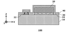
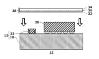
- FIG. 1 shows an example of an electronic device package 100 in this embodiment.
- An example of the protective sheet 38 in this embodiment is shown.
- An example of the flow length in this embodiment is shown.
- Another example of the protective sheet 38 in this embodiment is shown.
- An example of the flow of the manufacturing method of the electronic device package 100 of this embodiment is shown.
- An example of S200 in the flow of FIG. 5 is shown.
- An example of the mounting board 12 on which the protective layer 30 is formed is shown.
- An example of a metal-containing sheet 46 is shown.
- An example of S300 using a metal-containing sheet 46 is shown.
- FIG. 1 shows an example of an electronic device package 100 in this embodiment.
- the electronic device package 100 is a package in which an electronic device such as an IC chip is mounted, and has good electromagnetic wave shielding properties and heat dissipation properties.
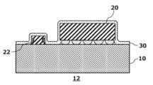
- the electronic device package 100 includes a circuit board 10 , electronic devices 20 and 22 (hereinafter also simply referred to as “electronic devices 20 and the like”), connection members 24 , a protective layer 30 and a conductive layer 40 .
- a conductive circuit (not shown) is provided on the surface of the circuit board 10, and the electronic device 20 and the like are mounted thereon.
- the circuit board 10 may be a printed wiring board, a mounting module board, or the like.
- the conductive circuit may be a circuit formed of a conductive metal such as copper or a material containing a conductive metal.
- the circuit board 10 may be a rigid board or a flexible board.
- the circuit board 10 may be processed as necessary.
- the circuit board 10 may be provided with printing, marking, dicing grooves, and the like.
- the electronic device 20 and the like are arranged on the circuit board 10 and exhibit various functions.
- the electronic device 20 or the like is, for example, an integrated circuit such as a memory chip, a power supply chip, a sound source chip, or a CPU chip, an active element such as a transistor or diode, or a capacitor such as a multilayer ceramic capacitor (MLCC), a thermistor, an inductor, a resistor, or the like.
- MLCC multilayer ceramic capacitor
- the MLCC has an external electrode on its side surface, and the need for insulation protection is particularly high from the viewpoint of preventing contact with other conductors and electric leakage.
- the entire MLCC components can be sufficiently insulated and protected by the protective layer 30 .
- the electronic device 20 and the like may have a cubic or rectangular parallelepiped shape.
- the electronic device 20 and the like may have a more complicated shape, and may have a polygon of pentagons or more when observed on the main surface of the circuit board (the XY plane in FIG. 1).
- the electronic device 20 and the like may have a hexagonal, octagonal, or other polygonal planar shape when viewed from the main surface.
- the electronic device 22 may be an inductor having an octagonal planar shape.
- the electronic device 20 and the like may have a polygon of pentagons or more when observed from the side surface of the main surface (the XZ plane or the YZ plane in FIG. 1, etc.).
- the electronic device 20 and the like may have a cubic or rectangular parallelepiped shape having concave or convex portions on the side surfaces, and the electronic device 22 may be an inductor having concave portions for forming coils on the side surfaces.
- a single or a plurality of electronic devices 20 and the like may be arranged on the circuit board 10 .
- the electronic devices 20 and the like may be formed in an n ⁇ m array on the circuit board 10 (n and m are integers equal to or greater than 2).
- the thickness of the electronic device 20 and the like is preferably 2000 ⁇ m or less. This is because if the thickness exceeds 2000 ⁇ m, there is a possibility that the protective layer 30 and the conductive layer 40 may be torn off due to the difference in level with the circuit board 10 when the protective layer 30 and the conductive layer 40 are formed. Moreover, it is desirable that the distance between the electronic devices 20 is 50 ⁇ m or more. This is because if the distance is less than 50 ⁇ m, the protective layer 30 and the conductive layer 40 may not be sufficiently formed.
- connection member 24 electrically connects the electronic device 20 or the like and the circuit board 10 .
- the connecting member 24 may include one or more of bumps such as solder balls arranged on the lower surface of the electronic device 20 and the like, lead frames on which the electronic device 20 and the like are mounted, and bonding wires. In the example of FIG. 1, bumps are used as connecting members 24 that connect the electronic device 20 and the circuit board 10 .
- the protective layer 30 is provided on the circuit board 10, the electronic device 20, etc., and protects the circuit board 10, the electronic device 20, etc. from electromagnetic waves, impacts, and the like.
- the protective layer 30 also serves to insulate and protect the circuit board 10 and the electronic device 20 from the conductive layer 40 .
- the protective layer 30 may cover all or part of the electronic devices 20 and the like and areas of the circuit board 10 where the electronic devices 20 and the like are not provided.
- the protective layer 30 may cover only the area of the circuit board 10 where the conductive circuit is provided, and may not cover the area without the conductive circuit.
- the protective layer 30 sufficiently covers the electronic device 20 or the like.
- the protective layer 30 of the present embodiment has a sufficient thickness at the corners. can be covered.
- the protective layer 30 may at least partially cover the connection member 24 .
- the protective layer 30 covers the side surfaces of the connection members 24, which are bumps. Even if the connecting members 24 include lead frames or bonding wires, the protective layer 30 may cover at least a portion of them.
- the protective layer 30 may be a cured thermosetting resin or the like.
- Protective layer 30 may include at least two layers.
- protective layer 30 may have two, three, four or more layers.
- the protective layer 30 preferably has three layers. Such a layer may be formed due to the layer structure of the protective sheet, which will be described later. The layer structure, material, etc. of the protective layer 30 will be described later.
- the film thickness of the protective layer 30 may vary depending on the location. For example, at the corners of the electronic device 20 and the like, the protective layer 30 may be thinner than the top surface of the electronic device 20 and the like. Further, for example, in a corner recess where the electronic device 20 or the like and the circuit board 10 are in contact with each other, the film thickness of the protective layer 30 may be thicker than the top surface of the electronic device 20 or the like.
- the conductive layer 40 is provided on the protective layer 30 to protect the electronic device 20 and the like from external electromagnetic waves and/or radiate heat generated from the electronic device 20 and the like to the outside.
- the conductive layer 40 may be a layer containing metal.
- the conductive layer 40 may be a metal thin film made of metal itself, or a resin layer in which conductive filler is dispersed. Details such as the material of the conductive layer 40 will be described later.
- the thickness of the conductive layer 40 may be 2 to 500 ⁇ m, preferably 5 to 100 ⁇ m, in the case of a thermosetting resin containing a conductive filler.
- the thickness may be 0.01 to 10 ⁇ m, preferably 0.1 to 5 ⁇ m. If the thickness is too thin, the electromagnetic wave shielding effect, the heat dissipation effect, and the mechanical strength may be insufficient, and if the thickness is too thick, the problem arises that the electronic device package 100 becomes unnecessarily large and bulky.
- the metal thin film and conductive filler used for the conductive layer 40 preferably have good electrical conductivity and/or thermal conductivity. ⁇ It may be K or more.
- the conductive layer 40 may be connected to the ground pattern exposed on the side surface or top surface of the circuit board 10 and/or the ground pattern of the electronic device 20 . Note that the electronic device package 100 may not have the conductive layer 40 .
- the protective layer 30 insulates and protects the electronic device 20 having a complicated shape and the connection member 24 . Further, according to the electronic device package 100, the heat generated by the electronic device 20 and the like can be released while the conductive layer 40 protects the electronic device 20 and the like from electromagnetic waves.
- the protective layer 30 can be formed of a protective sheet 38 as described below. According to the protective sheet 38, it is possible to sufficiently cover and insulate and protect the periphery of the electronic device 20 and the like having a complicated shape without causing air trapping between the protective layer 30 and the circuit board 10. did it.
- FIG. 2 shows an example of the protective sheet 38 in this embodiment.
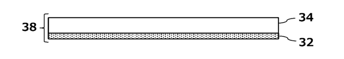
- the protective sheet 38 is a sheet for circuit boards, and is used to form the protective layer 30 shown in FIG. As shown, the protective sheet 38 has a first protective layer 32 , a second protective layer 34 and a third protective layer 36 .
- the protective sheet 38 has a first surface (lower side in FIG. 1) and a second surface opposite to the first surface (upper side in FIG. 1).
- the first surface side is the side that contacts the circuit board 10 and the electronic device 20
- the second surface side is the side that contacts the conductive layer 40 .
- the first protective layer 32 is the outermost layer on the first surface side of the protective sheet 38 .
- the second protective layer 34 is the outermost layer on the second surface side.
- a third protective layer 36 is provided between the first protective layer 32 and the second protective layer 34 .
- the protective sheet 38 has an adhesive strength of 0.15 N/cm 2 or less, preferably 0.12 N/cm 2 or less, and more preferably 0.10 N/cm 2 or less on the first surface measured by a probe tack test.
- the probe tack test is based on the Japanese Pharmacopoeia 18th revision general test method 6.
- Formulation test method 6.12 Adhesion strength test method 3.4 The same test method as the probe tack test method or a test method based thereon may be used.
- the adhesiveness of the protective sheet 38 is suppressed when the protective sheet 38 is arranged on the circuit board 10, and the unintended portion of the protective sheet 38 sticks to the circuit board 10 or spreads wet. It is possible to prevent that (so-called paddling).
- the protective sheet 38 has high tackiness, it may adhere to the circuit board 10 during pressing, thereby hindering the release of air (so-called air entrapment).
- the air can be smoothly removed.
- the adhesive strength of the second surface of the protective sheet 38 according to a probe tack test may be 0.01 N/cm 2 or more, preferably 0.05 N/cm 2 or more, and more preferably 0.10 N/cm 2 or more. Also, the difference in adhesive strength between the first surface and the second surface is 0.05 N/cm 2 to 0.40 N/cm 2 , preferably 0.05 N/cm 2 to 0.30 N/cm 2 , more preferably 0. .10 N/cm 2 to 0.20 N/cm 2 .
- the cushioning material can be laminated on the protective sheet for the purpose of applying an appropriate pressure to the protective sheet during hot pressing.
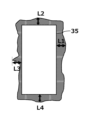
- FIG. 3 shows an example of the flow length in this embodiment.
- a protective sheet 38 was sandwiched between two polyimide films and cut into a standard rectangular shape of 0.5 cm x 1.0 cm. This was pressed at 1 MPa for 5 minutes while maintaining the temperature at 180°C. At this time, a part of the protective sheet 38 softens and flows from between the polyimide films, so the length from the polyimide film of the most flowing part is measured for each side.
- the flow is generated so as to protrude from four sides of a polyimide film 35 having the same shape (standard shape) as the protective sheet 38 before pressing.
- lengths L1 to L4 from the side of the most flowing portion are measured along a straight line extending from each side of the polyimide film 35 at 90 degrees.
- the flow length F total ( ⁇ m) be the average of the flow lengths L1 to L4 of the four sides expressed in units of ⁇ m.
- the index X When the index X is within the above range, a sufficient amount of the protective layer 30 is formed around the circuit board 10, the electronic device 20, etc., and the electronic device package 100 can be more reliably insulated and protected. On the other hand, if the index X is larger than the above range, the fluidity of the protective sheet 38 at the time of thermocompression bonding is too high, and a part of the protective layer 30 (for example, the corners of the electronic device 20 or the like) lacks thickness. occurs.
- the protective sheet 38 will not have sufficient fluidity during thermocompression bonding, and the electronic device 20 and the like will not be sufficiently insulated and protected by the protective layer 30, resulting in a risk of insufficient voltage resistance.
- the protective layer 30 may not be sufficiently formed around the reentrant corners where the circuit board 10 and the electronic device 20 or the like are in contact, around the connection member 24, and/or around the electronic device 20 or the like having a complicated shape (particularly the concave portion). be.
- the protective sheet 38 may have a tensile strength at break of 10 to 70 N/mm 2 , preferably 15 to 50 N/mm 2 , more preferably 20 to 40 N/mm 2 .
- Tensile breaking strength may be measured according to JIS-C-2151:2019.
- the tensile strength at break is determined by using a tensile tester to pull the protective sheet 38 at a speed of 50 mm/minute in an environment of 23° C. and 60% RH, and the strength when the protective sheet 38 breaks (tensile It may be calculated by calculating the load value/cross-sectional area of the protective sheet 38).
- the protective sheet 38 will not have sufficient fluidity during thermocompression bonding, and there is a risk that the electronic device 20 and the like will not be sufficiently insulated and protected by the protective layer 30 . If the tensile strength at break is too small, the fluidity of the protective sheet 38 at the time of thermocompression bonding is too high, causing a problem of insufficient thickness in a part of the protective layer 30 (for example, the corners of the electronic device 20 or the like). On the other hand, when the tensile breaking strength is within the above range, a sufficient amount of the protective layer 30 is formed around the circuit board 10, the electronic device 20, etc., and the electronic device package 100 can be more reliably insulated and protected.
- the protective sheet 38 may have a thickness of 50-500 ⁇ m, preferably 100-250 ⁇ m.
- the first protective layer 32 mainly has a role of imparting fluidity to the protective sheet 38 .
- the first protective layer 32 may have an index Z of 2.0 to 15.0, preferably 4.0 to 12.0, more preferably 5.0 to 10.0, which is obtained by the following formula 2.
- Z F1 / T1
- F 1 is the flow length of the most flowing portion on each side when the first protective layer 32 made into a rectangle of 0.5 cm ⁇ 1.0 cm is heated and pressed at 180 ° C. and 1 MPa for 5 minutes. Average ( ⁇ m).
- T 1 is the thickness ( ⁇ m) of the first protective layer 32 .
- F 1 may be measured in a similar manner as F total .
- the index Z takes a larger numerical range than the index X.
- the first protective layer 32 flows well when the protective sheet 38 is thermocompression-bonded, so that the surroundings (especially recesses) of the electronic device 20 having a complicated shape, the connection member 24, and/or the circuit board 10 and the electronic device 20 or the like can be entered.
- the index Z is larger than the above range, the fluidity becomes too high, which causes a problem of insufficient thickness in a part of the protective layer 30 (for example, the corners of the electronic device 20, etc.).
- the index Z is smaller than the above range, the fluidity of the protective sheet 38 during thermocompression bonding is insufficient, and there is a risk that the electronic device 20 and the like are not sufficiently insulated and protected by the protective layer 30 .
- the index Z is within the above range, a sufficient amount of the protective layer 30 is formed around the circuit board 10, the electronic device 20, etc., and the electronic device package 100 can be more reliably insulated and protected.
- the film thickness of the first protective layer 32 may be 5-150 ⁇ m, more preferably 5-50 ⁇ m, more preferably 10-30 ⁇ m.
- the adhesiveness of the protective sheet 38 can be suppressed and appropriate fluidity can be imparted.
- the glass transition temperature of the first protective layer 32 may be 80°C or lower, preferably 60°C or lower, and more preferably 50°C or lower.
- the glass transition temperature of the first protective layer 32 may be 20° C. or higher, preferably 30° C. or higher, and more preferably 35° C. or higher.
- the second protective layer 34 mainly has a role of preventing ion migration due to metal ions from the conductive layer 40 in contact while securing the thickness of the protective layer 30 .
- F2 is the flow length of the most flowing portion on each side when the second protective layer 34 made into a rectangle of 0.5 cm x 1.0 cm is heated and pressed at 180 ° C. and 1 MPa for 5 minutes. Average ( ⁇ m).
- T 2 is the thickness ( ⁇ m) of the second protective layer 34 .
- F2 may be measured in a similar manner as Ftotal .
- the index Y is within the above range, the second protective layer 34 does not flow excessively when the protective sheet 38 is thermocompression bonded, and the film thickness of the protective layer 30 such as the corners of the electronic device 20 is reduced. Remains firmly in areas that tend to become thin. Thereby, the electronic device package 100 can be insulated and protected more reliably. Moreover, when the conductive layer 40 is formed on the protective layer 30, ion migration from the conductive layer 40 can be sufficiently prevented.
- the index Y is larger than the above range, the fluidity of the protective sheet 38 during thermocompression bonding is too high, causing a problem of insufficient thickness in a part of the protective layer 30 (for example, corners of the electronic device 20, etc.).
- the index Y is smaller than the above range, the fluidity of the protective sheet 38 during thermocompression bonding is insufficient, and the electronic device 20 and the like are not sufficiently insulated and protected by the protective layer 30, and there is a risk of ion migration.
- the film thickness of the second protective layer 34 may be 10-200 ⁇ m, more preferably 30-150 ⁇ m, more preferably 50-100 ⁇ m. When the film thickness of the second protective layer 34 satisfies the above conditions, the film thickness of the entire protective layer 30 can be ensured while maintaining the heat dissipation of the electronic device 20 and the like.
- the second protective layer 34 may be thicker than the first protective layer 32 . In this case, it is possible to more reliably prevent the lack of thickness at a part of the protective layer 30 (for example, the corners of the electronic device 20 and the like). Also, the first protective layer 32 may be thicker than the second protective layer 34 . In this case, the protective layer 30 can more reliably protect the periphery (particularly the concave portion) of the electronic device 20 having a complicated shape, the connection member 24 , and/or the gap between the circuit board 10 and the electronic device 20 .
- the glass transition temperature of the second protective layer 34 may be 60°C or lower, preferably 50°C or lower, and more preferably 40°C or lower.
- the glass transition temperature of the second protective layer 34 may be 0° C. or higher, preferably 10° C. or higher, and more preferably 20° C. or higher.
- the glass transition temperature of the second protective layer 34 may be lower than the glass transition temperature of the first protective layer 32 .
- the second protective layer 34 mainly has a role of securing the thickness of the protective layer 30 while having certain fluidity.
- F3 is the flow length of the most flowing portion on each side when the third protective layer 36 made into a rectangle of 0.5 cm x 1.0 cm is heated and pressed at 180 ° C. and 1 MPa for 5 minutes. Average ( ⁇ m).
- T 3 is the thickness ( ⁇ m) of the third protective layer 36 .
- F3 may be measured in a similar manner as Ftotal .
- the index W takes a numerical range between the index Y and the index Z.
- the third protective layer 36 has fluidity between the first protective layer 32 and the second protective layer 34 when the protective sheet 38 is thermocompression-bonded, and the first protective layer 32 and the second protective layer 34 are coated. has the effect of complementing
- the film thickness of the third protective layer 36 may be 20-200 ⁇ m, more preferably 30-150 ⁇ m, more preferably 40-80 ⁇ m.
- the surroundings (especially concave portions) of the electronic device 20 having a complicated shape, the connection member 24, and/or the gap between the circuit board 10 and the electronic device 20, etc. can be filled. It is possible to achieve the effect of protecting such as by the protective layer 30 and the effect of firmly remaining in the portion where the film thickness of the protective layer 30 tends to be thin.
- the third protective layer 36 may be composed of a plurality of layers.
- the third protective layer 36 may be configured by laminating two identical resin films.
- the third protective layer 36 may be thicker than the first protective layer 32 . In this case, it is possible to more reliably prevent the lack of thickness at a part of the protective layer 30 (for example, the corners of the electronic device 20 and the like). Also, the first protective layer 32 may be thicker than the third protective layer 36 . In this case, the protective layer 30 can more reliably protect the periphery (particularly the concave portion) of the electronic device 20 having a complicated shape, the connection member 24 , and/or the gap between the circuit board 10 and the electronic device 20 .
- the glass transition temperature of the third protective layer 36 may be 60°C or lower, preferably 50°C or lower, and more preferably 40°C or lower.
- the glass transition temperature of the third protective layer 36 may be 0° C. or higher, preferably 10° C. or higher, and more preferably 20° C. or higher.
- the glass transition temperature of the third protective layer 36 may be lower than the glass transition temperature of the first protective layer 32 . Thereby, the impact absorption of the third protective layer 36 is improved, and the impact absorption of the protective layer 30 as a whole can be enhanced.
- the second protective layer 34 may have a harder property than the first protective layer 32 .
- the Young's modulus of the second protective layer 34 may be higher than that of the first protective layer 32 .
- the Young's modulus of the first protective layer 32 at 120.degree.
- the Young's modulus of the third protective layer 36 may be intermediate between that of the first protective layer 32 and the second protective layer 34, eg, 1.5 to 3.5 at 120.degree. Since the first protective layer 32 to the third protective layer 36 have such a Young's modulus, the protective sheet 38 can exhibit appropriate fluidity under high temperatures at which hot pressing is performed.
- the first protective layer 32, the second protective layer 34 and the third protective layer 36 may be thermosetting resin.
- the first protective layer 32, the second protective layer 34 and the third protective layer 36 may contain a thermosetting resin and a curing agent.
- thermosetting resin a polymer having at least one functional group in one molecule that undergoes a cross-linking reaction upon heating may be used.
- functional groups include hydroxyl group, phenolic hydroxyl group, methoxymethyl group, carboxyl group, amino group, epoxy group, oxetanyl group, oxazoline group, oxazine group, aziridine group, thiol group, isocyanate group, blocked isocyanate group, blocked One or more of carboxyl groups, silanol groups, and the like may be used.
- thermosetting resins include polyurethane resins, acrylic resins, maleic acid resins, polybutadiene resins, polyester resins, urea resins, epoxy resins, oxetane resins, phenoxy resins, polyimide resins, and polyamides. resins, polyamideimide resins, phenolic resins, cresol resins, melamine resins, alkyd resins, amino resins, polylactic acid resins, oxazoline resins, benzoxazine resins, silicone resins, and fluorine resins. One or more of resins and the like may be used. Two or three of the first protective layer 32, the second protective layer 34, and the third protective layer 36 may use the same or similar resin as a thermosetting resin.
- a curing agent one or more of epoxy curing agents, aziridine curing agents, phenol curing agents, amine curing agents, isocyanate curing agents, metal chelate curing agents, etc. may be used.
- An aziridine curing agent is a curing agent containing a compound having an aziridine group
- a phenolic curing agent is a curing agent containing a compound having a structure in which a hydroxy group is directly linked to an aromatic group (aromatic ring)
- an amine may be a curing agent containing a compound having an amino group
- the isocyanate curing agent may be a curing agent containing a compound containing an isocyanate group.
- the metal chelate-based curing agent may be a curing agent containing a complex formed by coordinating a multidentate ligand (chelate ligand) to a metal ion.
- Two or three of the first protective layer 32, the second protective layer 34 and the third protective layer 36 may use the same or similar curing agents.
- the epoxy-based curing agent may be an epoxy compound.
- An epoxy compound is a compound having two or more epoxy groups in one molecule.
- the properties of the epoxy compound may be liquid or solid.
- the epoxy compound may be, for example, a glycidyl ether type epoxy compound, a glycidyl amine type epoxy compound, a glycidyl ester type epoxy compound, a cycloaliphatic (alicyclic type) epoxy compound, or the like.
- Examples of glycidyl ether type epoxy compounds include bisphenol A type epoxy compounds, bisphenol F type epoxy compounds, bisphenol S type epoxy compounds, bisphenol AD type epoxy compounds, cresol novolac type epoxy compounds, phenol novolak type epoxy compounds, ⁇ -naphthol novolak. type epoxy compound, bisphenol A type novolac type epoxy compound, dicyclopentadiene type epoxy compound, tetrabromobisphenol A type epoxy compound, brominated phenol novolac type epoxy compound, tris(glycidyloxyphenyl)methane, tetrakis(glycidyloxyphenyl)ethane , etc., may be selected from one or more.
- glycidylamine-type epoxy compounds include tetraglycidyldiaminodiphenylmethane, triglycidyl para-aminophenol, triglycidylmethaminophenol, tetraglycidylmethaxylylenediamine, and the like.
- glycidyl ester-type epoxy compounds examples include diglycidyl phthalate, diglycidyl hexahydrophthalate, and diglycidyl tetrahydrophthalate.
- Cycloaliphatic (alicyclic) epoxy compounds include, for example, epoxycyclohexylmethyl-epoxycyclohexanecarboxylate, bis(epoxycyclohexyl)adipate, and the like.
- a liquid epoxy compound may also be used.
- the aziridine-based curing agent may be an aziridine compound.
- aziridine compounds include N,N'-diphenylmethane-4,4'-bis(1-aziridine carboxysite), N,N'-toluene-2,4-bis(1-aziridine carboxysite), bisiso phthaloyl-1-(2-methylaziridine), tri-1-aziridinylphosphine oxide, N,N'-hexamethylene-1,6-bis(1-aziridinecarboxysite), trimethylolpropane-tri- ⁇ - aziridinyl propionate, tetramethylolmethane - tri- ⁇ -aziridinyl propionate, tris-2,4,6-(1-aziridinyl)-1,3,5-triazine, trimethylolpropane tris [ 3-(1-aziridinyl) propionate], trimethylolpropane tris [3-(1-a
- the phenol-based curing agent may be a phenol compound.
- the phenolic compound may be a phenolic resin having two or more phenolic hydroxyl groups in one molecule. It may be selected from one or more of phenolic resins, triphenylmethane-type phenolic resins, novolac-type phenolic resins, dicyclopentadiene-type phenolic resins, xylylene-type phenolic resins, and biphenyl-type phenolic resins.
- the amine-based curing agent may be an amine compound.
- the amine compound may be a compound having two or more amino groups and may be dimer diamine or other polyamines.
- the isocyanate curing agent may be an isocyanate compound.
- the isocyanate compound may be selected from one or more of aromatic polyisocyanates, aliphatic polyisocyanates, cycloaliphatic polyisocyanates.
- aromatic polyisocyanates examples include 1,3-phenylene diisocyanate, 1,4-phenylene diisocyanate, 2,4-tolylene diisocyanate (TDI), 2,6-tolylene diisocyanate, 4,4′-diphenylmethane diisocyanate ( MDI), 2,4-diphenylmethane diisocyanate, 4,4'-diisocyanatobiphenyl, 3,3'-dimethyl-4,4'-diisocyanatobiphenyl, 3,3'-dimethyl-4,4'-di isocyanatodiphenylmethane, 1,5-naphthylene diisocyanate, 4,4′,4′′-triphenylmethane triisocyanate, m-isocyanatophenylsulfonyl isocyanate, p-isocyanatophenylsulfonyl isocyanate and the like.
- aliphatic polyisocyanates examples include ethylene diisocyanate, tetramethylene diisocyanate, hexamethylene diisocyanate (HDI), dodecamethylene diisocyanate, 1,6,11-undecane triisocyanate, 2,2,4-trimethylhexamethylene diisocyanate, and lysine diisocyanate. , 2,6-diisocyanatomethylcaproate, bis(2-isocyanatoethyl) fumarate, bis(2-isocyanatoethyl) carbonate, 2-isocyanatoethyl-2,6-diisocyanatohexanoate, etc. mentioned.
- alicyclic polyisocyanates examples include isophorone diisocyanate (IPDI), 4,4′-dicyclohexylmethane diisocyanate (H12-MDI), cyclohexylene diisocyanate, methylcyclohexylene diisocyanate (hydrogenated TDI), bis(2-isocyanato ethyl)-4-cyclohexene-1,2-dicarboxylate, 2,5-norbornane diisocyanate, 2,6-norbornane diisocyanate and the like.
- IPDI isophorone diisocyanate
- H12-MDI 4,4′-dicyclohexylmethane diisocyanate
- cyclohexylene diisocyanate methylcyclohexylene diisocyanate
- hydrogenated TDI hydrogenated TDI
- trimethylolpropane adducts of diisocyanates are also included.
- the blocked isocyanate compound is not particularly limited as long as it is a blocked isocyanate group-containing compound in which the isocyanate group in the isocyanate group-containing compound is protected with ⁇ -caprolactam, MEK oxime, or the like.
- the isocyanate groups of the isocyanate group-containing compounds are blocked with ⁇ -caprolactam, MEK oxime, cyclohexanone oxime, pyrazole, phenol, and the like.
- the hexamethylene diisocyanate trimer having an isocyanurate ring and blocked with MEK oxime or pyrazole has not only storage stability but also adhesion to bonding materials such as polyimide and copper when used in this embodiment. It is very preferable because it is excellent in strength and solder heat resistance.
- the metal chelate curing agent may be selected from one or more of aluminum chelate compounds, titanium chelate compounds, and zirconium chelate compounds.
- the central metal may be selected from iron, cobalt, indium, and the like.
- the curing agent may be used in an amount of 1 to 50 parts by weight, preferably 10 to 40 parts by weight, and more preferably 20 to 30 parts by weight with respect to 100 parts by weight of the thermosetting resin.
- the fluidity and tackiness of the first protective layer 32, the second protective layer 34 and the third protective layer 36 may be adjusted by adjusting the amount of the curing agent.
- the second protective layer 34 has the highest hardener content
- the third protective layer 36 has the next highest hardener content
- the first protective layer 32 contains no hardener or the third protective layer Curing agents may be included in amounts of 36 or less.
- the first protective layer 32, the second protective layer 34 and the third protective layer 36 may further contain a filler.
- the filler is preferably insulating and may be selected from, for example, inorganic fillers, phosphorus-based fillers, nitrogen-based fillers, fluorine-based fillers, and polymeric fillers. One type or a plurality of types may be used as the filler.
- Inorganic fillers include silica, hollow silica, porous silica, mica, talc, kaolin, clay, hydrotalcite, wollastonite, xonotlite, silicon nitride, boron nitride, aluminum nitride, calcium hydrogen phosphate, calcium phosphate, glass flakes, hydrated glass, calcium titanate, sepiolite, magnesium sulfate, aluminum hydroxide, magnesium hydroxide, zirconium hydroxide, barium hydroxide, calcium hydroxide, titanium oxide, tin oxide, aluminum oxide, magnesium oxide, zirconium oxide, zinc oxide , molybdenum oxide, antimony oxide, nickel oxide, zinc carbonate, magnesium carbonate, calcium carbonate, barium carbonate, zinc borate, aluminum borate, inorganic ion scavengers (for example, IXE (registered trademark) manufactured by Toagosei Co., Ltd.) mentioned.
- IXE registered trademark
- Phosphorus-based fillers include (poly ) Phosphate compounds, organic phosphate compounds, phosphazene compounds, phosphonic acid compounds, aluminum diethylphosphinate, aluminum methylethylphosphinate, aluminum diphenylphosphinate, aluminum ethylbutylphosphinate, aluminum methylbutylphosphinate, polyethylenephosphine Examples include phosphinic acid compounds such as aluminum oxide, phosphine oxide compounds, phosphorane compounds, and phosphoramide compounds.
- Nitrogen-based fillers include nitrogen-based fillers such as benzoguanamine, melamine, melam, melem, melon, melamine cyanurate, cyanuric acid compounds, isocyanuric acid compounds, triazole compounds, tetrazole compounds, diazo compounds, and urea.
- fluorine-based fillers polytetrafluoroethylene powder and modified products thereof, tetrafluoroethylene-perfluoroalkyl vinyl ether powder, tetrafluoroethylene-ethylene powder, tetrafluoroethylene-hexafluoropropylene powder, tetrafluoroethylene-vinylidene fluoride powder, Tetrafluoroethylene-hexafluoropropylene-perfluoroalkyl vinyl ether powder, polychlorotrifluoroethylene powder, chlorotrifluoroethylene-ethylene powder, chlorotrifluoroethylene-vinylidene fluoride powder, polyvinylidene fluoride powder, polyvinyl fluoride powder, etc. mentioned.
- Polymer fillers include polyethylene powder, polyacrylate powder, epoxy resin powder, polyamide powder, polyimide powder, polyurethane powder, liquid crystal polymer beads, polysiloxane powder, silicone, acryl, styrene-butadiene rubber, butadiene rubber, etc.
- a core-shell having a multi-layered structure, etc., can be mentioned.
- the average particle size D 50 of the filler may be 0.01-100 ⁇ m, preferably 0.02-40 ⁇ m, more preferably 0.05-20 ⁇ m.
- the second protective layer 34 and the third protective layer 36 may contain 0.1 to 30% by weight, preferably 1 to 25% by weight, more preferably 5 to 20% by weight of filler.
- the index X, index Y and/or index Z (fluidity) can be adjusted so as to approach an appropriate range.
- the first protective layer 32 may contain no filler, or may contain filler at a lower mass concentration than the second protective layer 34 and the third protective layer 36 .
- the first protective layer 32 contains a filler, it is 0.01 to 1 part by weight, preferably 0.01 to 0.5 part by weight, more preferably 0.01 to 1 part by weight with respect to 100 parts by weight of the thermosetting resin. 0.1 part by weight.
- the second protective layer 34 has the highest filler content
- the third protective layer 36 has the second highest filler content
- the first protective layer 32 does not contain any filler or less than the third protective layer 36.
- the filler may be included at a mass concentration of
- the protective sheet 38 contains a filler
- the mass concentration of the filler on the second surface side of the protective sheet 38 is higher than that on the first surface side.
- the tackiness (adhesiveness) of the first protective layer 32 that is, the first surface side
- the adhesive strength of the first surface of the protective sheet 38 in a probe tack test can be adjusted to a predetermined value or less.
- the amount of filler and/or the amount of curing agent it becomes easier to adjust the fluidity in the order of the first protective layer 32, the third protective layer 36, and the second protective layer 34.
- the second protective layer 34 and the third protective layer 36 contain the same amount of filler, and the first protective layer 32 contains no filler, or the second protective layer 34 and the third protective layer 36 or less.
- the filler may be included at a mass concentration of
- the third protective layer 36 has the highest filler content
- the second protective layer 34 has the next highest filler content
- the first protective layer 32 does not contain any filler or the third protective layer It may contain fillers at a mass concentration of 36 or less.
- the filler content is 0.1 to 30.0% by weight, preferably 1.0 to 9.8% by weight, more preferably 3.5 to 8.5% by weight. % by weight. If the amount of filler in the entire protective sheet 38 is lower than this range, the fluidity will be too high, and if it is higher, cracks will occur in the protective layer during cooling/heating cycles, which may cause poor appearance.
- the filler content in the entire protective sheet 38 is only an additional improvement item and is not essential.
- the first protective layer 32, the second protective layer 34 and the third protective layer 36 may further contain a thermoplastic resin.
- a thermoplastic resin it is preferable to select one or more from, for example, polyester, acrylic resin, polyether, urethane resin, styrene elastomer, polycarbonate, butadiene rubber, polyamide, esteramide resin, polyisoprene, and cellulose.
- a thermoplastic resin it is preferably contained in each layer of the first protective layer 32, the second protective layer 34 and/or the third protective layer 36 in an amount of 5 to 40% by weight.
- the first protective layer 32, the second protective layer 34 and the third protective layer 36 may further contain additives.
- additives include colorants (e.g., pigments, dyes, or carbon powders such as carbon black, carbon nanotubes, graphene, fullerene), flame retardants, antiblocking agents, metal deactivators, thickeners, dispersants. , silane coupling agents, rust inhibitors, copper damage inhibitors, reducing agents, antioxidants, tackifying resins, plasticizers, ultraviolet absorbers, antifoaming agents, leveling modifiers, etc. types may be used.
- colorants e.g., pigments, dyes, or carbon powders such as carbon black, carbon nanotubes, graphene, fullerene
- flame retardants e.g., flame retardants, antiblocking agents, metal deactivators, thickeners, dispersants.
- silane coupling agents e.g., rust inhibitors, copper damage inhibitors, reducing agents, antioxidants, tackifying resins,
- FIG. 4 shows another example of the protective sheet 38 in this embodiment.
- the protective sheet 38 may be composed of only the first protective layer 32 and the second protective layer 34 and may not include the third protective layer 36 .
- the configurations, materials, etc. of the first protective layer 32 and the second protective layer 34 may be as described above.
- first protective layer 32, the second protective layer 34 and the third protective layer 36 may be provided with multiple layers.
- the protective sheet 38 may have one first protective layer 32, one second protective layer 34, and a plurality of third protective layers 36 sandwiched therebetween.
- the protective sheet 38 may contain other layers as needed.
- the protective sheet 38 may further have a peeling layer or the like that is peeled off after being attached to the circuit board 10 . If a release layer is provided, it may be provided further above the second protective layer 34 (opposite to the first protective layer 32).
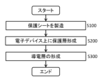
- FIG. 5 shows an example of the flow of the method for manufacturing the electronic device package 100 of this embodiment.
- the electronic device package 100 may be manufactured by performing at least part of S100 to S300.
- S100 to S300 are described in this order, but these processes may be performed in a different order and/or at least partially may be performed in parallel.
- a protective sheet 38 for forming the protective layer 30 is manufactured.
- the protective sheet 38 may be as described in FIGS. 2-4.
- the method for manufacturing the protective sheet 38 is not particularly limited, but for example, the materials such as the above-described thermosetting resins forming the layers (the first protective layer 32, the second protective layer 34, and the third protective layer 36) of the protective sheet 38 is dissolved in a solvent or the like and successively applied and dried to form a laminated structure, or a method of laminating the composition that has been pre-cured or semi-cured.
- coating methods include gravure coating, kiss coating, die coating, lip coating, comma coating, blade coating, roll coating, knife coating, spray coating, bar coating, spin coating, dip coating, Alternatively, various printing methods may be used.
- the protective layer 30 formed from the protective sheet 38 is formed on the mounting substrate 12.
- the mounting board 12 is prepared.
- the mounting board 12 may be a circuit board 10 having a surface provided with a conductive circuit, on which the electronic device 20 and the like are mounted.
- the protective sheet 38 manufactured in S100 is placed on the mounting substrate 12 so that the first protective layer 32 (first surface side) faces the electronic device 20 side.
- FIG. 6 shows an example of S200 in the flow of FIG.
- the protective sheet 38 may be attached to the mounting board 12 after the protective sheet 38 is arranged so that the first protective layer 32 faces the electronic device 20 and the like.
- the mounting substrate 12 may be heat-pressed.
- the uncured or semi-cured thermosetting resin of each protective layer of the protective sheet 38 can be cured.
- the protective sheet 38 becomes the protective layer 30 .
- the release sheet may be removed from protective sheet 38 after hot pressing.
- the heat press may be performed under reduced pressure or under vacuum. Thereby, the degree of adhesion of the first protective layer 32 to the mounting substrate 12 can be enhanced.
- Hot press is performed at 100 to 220° C., preferably 120 to 200° C., more preferably 140 to 180° C., for 1 to 120 minutes, preferably 1 to 40 minutes, more preferably 1 to 10 minutes at 0.1 to 10 MPa. , preferably 0.5 to 3 MPa, more preferably 1 to 2 MPa.
- additional heating it may be performed under the same temperature conditions and the like as the heat press.
- each layer that constitutes the protective sheet 38 softens before being completely cured, and flows to the side surfaces of the connection members 24 such as recesses at the corners of the circuit board 10 and the electronic device 20 and bumps.
- the first protective layer 32 which has higher fluidity than the other layers, sufficiently protects the portions where the protective layer 30 is difficult to be formed by flowing to these portions. This can prevent contact between the connection member 24 and other conductors and electric leakage.
- the second protective layer 34 and the third protective layer 36 which have relatively low fluidity, do not move significantly even when hot-pressed, so they remain in the entire electronic device 20 and the like in a certain amount. As a result, it is possible to more reliably prevent the lack of thickness in a part of the protective layer 30 (for example, the corners of the electronic device 20 and the like).
- FIG. 7 shows an example of the mounting board 12 on which the protective layer 30 is formed. As described above, by curing the protective sheet 38, the protective layer 30 is formed and the entire surface of the mounting board 12 is insulated and protected.
- the protective sheet 38 that does not include a release sheet was given, but the present invention is not limited to this.
- the protective sheet 38 having a release sheet on the second protective layer 34 side may be used for hot pressing, and the release sheet may be peeled off after the hot pressing.
- the conductive layer 40 is formed on the protective layer 30. As shown in FIG.
- the conductive layer 40 may be formed partially or entirely in the region where the protective layer 30 is formed.
- Conductive layer 40 may be formed by transferring metal from metal-containing sheet 46 to mounting substrate 12 .
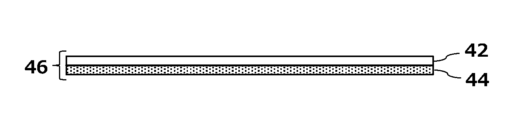
- FIG. 8 shows an example of the metal-containing sheet 46.
- the metal-containing sheet 46 is obtained by forming the metal material layer 44 on the release sheet 42 .
- the release sheet 42 a film-like release base material that can be peeled off later, or a release resin having cushioning properties can be used.
- the release sheet 42 may be composed of a single layer or multiple layers of release substrate and/or release resin.
- the release base material is a film-like base material having releasability on one side or both sides.
- the release substrate is desirably a sheet having a tensile breaking strain of less than 50% at 150°C.
- release substrates include polyethylene terephthalate, polyethylene naphthalate, polyvinyl fluoride, polyvinylidene fluoride, rigid polyvinyl chloride, polyvinylidene chloride, nylon, polyimide, polystyrene, polyvinyl alcohol, ethylene-vinyl alcohol copolymer, polycarbonate, poly Plastic sheets such as acrylonitrile, polybutene, soft polyvinyl chloride, polyvinylidene fluoride, polyethylene, polypropylene, polyurethane resin, ethylene vinyl acetate copolymer, polyvinyl acetate, etc. Paper such as glassine paper, fine paper, kraft paper, coated paper, etc. , various nonwoven fabrics, synthetic papers, metal foils, or composite films
- the release resin is a resin that conforms to the shape of the electronic device 20 and the like, and also has releasability.
- the release resin is a resin that can be released after hot pressing or the like for the releasing cushion member.
- the release resin preferably has a tensile breaking strain of 50% or more at 150°C. Also, the release resin is preferably melted during hot pressing.
- release resins include those selected from one or more of polyethylene, polypropylene, polyethersulfone, polyphenylene sulfide, polystyrene, polymethylpentene, polybutylene terephthalate, cyclic olefin polymer, and silicone.
- polypropylene, polymethylpentene, polybutylene terephthalate, and silicone are suitable from the viewpoint of compatibility between embeddability and peelability.
- the metal material layer 44 may be made of a conductive paste containing a thermosetting resin and a conductive filler.
- the metal material layer 44 may be formed by applying a conductive paste on the release sheet 42 and drying the solvent.
- the thermosetting resin in the conductive paste is preferably in an uncured or semi-cured state. Examples of the coating method include the method of coating the composition of each protective layer described above and the method of screen printing.
- thermosetting resin the same one as used for forming the first to third protective layers can be used.
- Examples of conductive fillers include metal particles, carbon particles, and conductive resin particles.
- the conductive filler may contain metal particles as an essential component, and may additionally contain one or more selected types of other components such as carbon particles.
- metal particles examples include gold, platinum, silver, copper, nickel, aluminum, iron, and alloys thereof, but copper is preferred in terms of price and conductivity.
- the metal particles may be particles comprising a nucleus made of a metal and a coating layer covering the nucleus and made of a metal different from the nucleus.
- the metals listed above are used as the core and coating layer. Examples thereof include silver-coated copper particles having a nucleus composed of copper and a coating layer composed of silver.
- Examples of carbon particles include those selected from one or more of acetylene black, ketjen black, furnace black, carbon nanotube, carbon nanofiber, graphite, fullerene, carbon nanowall, and graphene.
- Examples of conductive resin particles include those selected from one or more of poly(3,4-ethylenedioxythiophene), polyacetylene, polythiophene, and the like.
- the average particle diameter D50 of the conductive filler is preferably about 1 to 100 ⁇ m, more preferably about 3 to 75 ⁇ m, even more preferably about 5 to 50 ⁇ m.
- the average particle size of the conductive filler can be measured by a laser diffraction method, a scattering method, or the like. For example, the average value of the diameters of a circle having a projected area equal to the projected area of the filler particle aggregate is obtained as the average particle size.
- the shape of the conductive filler may be spherical, needle-like, scale-like, flake-like, dendritic, grape-like, fibrous, or plate-like.
- the content of the conductive filler in the metal material layer 44 is not particularly limited, but is preferably 100 to 1500 parts by weight, more preferably 100 to 1000 parts by weight, with respect to 100 parts by weight of the thermosetting resin. preferable.
- the conductive layer 40 can be provided with necessary and sufficient conductivity, and the electromagnetic wave shielding effect can be sufficiently enhanced, regardless of the type of the conductive particles. It is also preferable because the fluidity of the composition containing the thermosetting resin and the conductive filler is increased, making it easier to form the metal material layer 44 .
- the metal material layer 44 may further contain a thermoplastic resin.
- a thermoplastic resin the same one that can be used for the first to third protective layers may be used.
- the metal material layer 44 may contain other additives.
- additives include cross-linking agents, colorants, flame retardants, fillers, lubricants, antiblocking agents, metal deactivators, thickeners, dispersants, silane coupling agents, rust inhibitors, and copper damage inhibitors. , reducing agents, antioxidants, tackifying resins, plasticizers, UV absorbers, defoamers, leveling modifiers, and the like.
- cross-linking agents include compounds that cross-link with the functional groups of thermosetting resins.
- a phenol-based curing agent an amine-based curing agent, an isocyanate-based curing agent, an epoxy-based curing agent, an aziridine-based curing agent, and a metal chelate-based curing agent may be used as the cross-linking agent.
- coloring agent for example, one or a plurality of organic pigments, carbon black, ultramarine blue, red iron oxide, zinc oxide, titanium oxide, graphite, and dyes may be used.
- flame retardant for example, one or more of halogen-containing flame retardants, phosphorus-containing flame retardants, nitrogen-containing flame retardants, inorganic flame retardants, and the like may be used.
- fillers for example, one or more of glass fibers, silica, talc, ceramics, and the like may be used.
- lubricant for example, one or more of fatty acid esters, hydrocarbon resins, paraffins, higher fatty acids, fatty acid amides, fatty alcohols, metallic soaps, and modified silicones may be used.
- antiblocking agent for example, one or more of calcium carbonate, silica, polymethylsilsesquiosane, aluminum silicate, and the like may be used.
- the metal material layer 44 may be a metal foil.
- the metal foil may be formed on the release sheet 42 by plating or the like with a metal similar to that exemplified for the conductive filler.
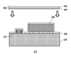
- FIG. 9 shows an example of S300 using the metal-containing sheet 46.
- the metal material layer 44 side of the metal-containing sheet 46 is placed on and attached to the protective layer 30 .
- the conductive layer 40 is formed by hot-pressing the metal-containing sheet 46 to cure the thermosetting resin of the metal material layer 44 .
- the release sheet 42 is removed. Thereby, the electronic device package 100 as shown in FIG. 1 is manufactured.
- the heat press may be performed under reduced pressure or under vacuum. Thereby, the degree of adhesion of the metal material layer 44 to the mounting board 12 can be enhanced. Hot pressing is performed at 100 to 220° C. (preferably 120 to 180° C.) for 1 to 120 minutes (preferably 1 to 60 minutes) at 0.1 to 10 MPa (preferably 0.5 to 3 MPa). good.
- the conductive layer 40 may be formed by another method without using the metal-containing sheet 46.
- the conductive layer 40 may be formed by depositing metal by plating, vapor deposition, or sputtering (hereinafter also referred to as “plating, etc.”). Examples of metals used for plating and the like include gold, platinum, silver, copper, nickel, aluminum, iron, and alloys thereof.
- the conductive layer 40 can be formed by coating or spraying a conductive paste (eg, one that can be used for the metal material layer 44) onto the protective layer 30 or the second protective layer 34 (prior to heat pressing). , which may be cured and formed.
- a step of singulating the electronic device package 100 may be performed.
- the electronic device package 100 may be diced in the X and Y directions at locations corresponding to product areas to obtain individual products.
- the electronic device package 100 without the conductive layer 40 may be used without performing S300.
- the protective layer 30 is formed on the mounting substrate 12 using the protective sheet 38 having a predetermined configuration and physical properties through the processes of S100 to S300.
- the protective layer 30 can be formed with a sufficient thickness even in portions where the protective layer 30 such as the corners of the electronic device 20 tends to flow too much and the film thickness tends to be thin, and in portions where the protective layer 30 does not flow sufficiently.
- the protective sheet 38 is pasted together, the first surface side can be prevented from adhering to the circuit board 10 or the like and causing paddling.
- the protective layer 30 may include a layer structure derived from the protective sheet 38.
- the protective sheet 38 has a three-layer structure
- at least part of the protective layer 30 may have a three-layer structure derived from the first protective layer 32 to the third protective layer 36, respectively.
- the film thickness of the protective layer 30 is increased, and the layered structure of the protective sheet 38 tends to remain.
- the layer structure of the protective sheet 38 may not remain at the corners of the electronic device 20 or the like where the thickness of the protective layer 30 is thin.
- composition A1 for the first protective layer 32 having the following composition was prepared.
- Polyurethane resin (acid value: 5 mgKOH / g, weight average molecular weight: 54,000, Tg: -7 ° C., manufactured by Toyochem) 100 parts by weight
- Epoxy compound (YDF-2005RD manufactured by Nippon Steel Chemical & Materials Co., Ltd.) 20 parts by weight
- Solvent methyl ethyl ketone
- composition A2 for first protective layer Silica (manufactured by Admatechs SO-C6, D50 ; 2.0 ⁇ m) was added.
- composition A3 for first protective layer Silica (manufactured by Admatechs SO-C6, D50 A composition A3 for the first protective layer 32 having the same composition as the composition A1 was prepared, except that 12 parts by weight of 2.0 ⁇ m) was added.
- composition A4 for first protective layer Silica (manufactured by Admatechs SO-C6, D50 2.0 ⁇ m) was added by 15 parts by weight.
- composition A5 for first protective layer Silica (manufactured by Admatechs SO-C6, D50 A composition A5 for the first protective layer 32 having the same composition as the composition A1 was prepared, except that 55 parts by weight of 2.0 ⁇ m) was added.
- composition A6 for first protective layer Silica (manufactured by Admatechs SO-C6, D50 ; 2.0 ⁇ m) was added by 1.5 parts by weight.
- composition A7 for first protective layer Silica (manufactured by Admatechs SO-C6, D50 A composition A7 for the first protective layer 32 having the same composition as the composition A1 was prepared, except that 20 parts by weight of 2.0 ⁇ m) was added.
- composition B1 for the second protective layer 34 having the following composition was prepared.
- Polyurethane resin (acid value: 5 mg KOH / g, weight average molecular weight: 54,000, Tg: -7 ° C., manufactured by Toyochem) 100 parts by weight
- Epoxy compound (YDF-2001 manufactured by Nippon Steel Chemical & Materials Co., Ltd.) 20 parts by weight
- Silica (ad Matex SO-C6, D50 ; 2.0 ⁇ m) 13.6 parts by weight (10% by weight of solid content excluding solvent)
- Solvent methyl ethyl ketone
- composition B2 Talc (FH104 D 50 manufactured by Fuji Talc Co., Ltd.) A composition B2 for the second protective layer 34 having the same composition as the composition C1 was prepared, except that it was changed to 24.4 parts by weight.
- composition B3 for the second protective layer 34 was prepared having the same composition as composition B1 except that the content of silica was changed to 35.0 parts by weight.
- composition B4 for the second protective layer 34 was prepared having the same composition as composition B1 except that no silica was added.
- composition C1 for the third protective layer 36 having the following composition was prepared.
- Polyurethane resin (acid value: 5 mg KOH / g, weight average molecular weight: 54,000, Tg: -7 ° C., manufactured by Toyochem) 100 parts by weight Epoxy compound (YDF-170 manufactured by Nippon Steel Chemical & Materials Co., Ltd.) 20 parts by weight Silica (ad Matex SO-C6, D50 ; 2.0 ⁇ m) 13.6 parts by weight Solvent (methyl ethyl ketone) 20 parts by weight [Third protective layer composition C2]
- a composition C2 for the third protective layer 36 was prepared having a composition similar to composition C1, except that no silica was added.
- Composition A1 was applied onto a release sheet. After that, it was heated at 120° C. for 5 minutes, dried and semi-cured to form a single layer A1 corresponding to the first protective layer 32 with a thickness of 15 ⁇ m.
- Composition B1 was applied onto a release sheet. After that, it was heated at 120° C. for 5 minutes, dried and semi-cured to form a single layer B1 corresponding to the second protective layer 34 with a thickness of 45 ⁇ m.
- Composition C1 was applied onto a release sheet. After that, it was heated at 120° C. for 5 minutes, dried and semi-cured to form a single layer C1 corresponding to the third protective layer 36 with a film thickness of 60 ⁇ m.
- composition A1 was applied onto a release sheet. After that, it was heated at 120° C. for 5 minutes, dried and semi-cured to form the first protective layer 32 having a thickness of 15 ⁇ m.
- a composition 1C was applied on the first protective layer 32 . After that, it was heated at 120° C. for 5 minutes, dried and semi-cured to form a third protective layer 36 having a thickness of 60 ⁇ m.
- composition B1 was applied onto the third protective layer 36 . After that, it was heated at 120° C. for 5 minutes, dried and semi-cured to form a second protective layer 34 having a thickness of 45 ⁇ m.
- a protective sheet H1 composed of the first protective layer 32, the third protective layer 36 and the second protective layer was formed.
- Protective sheet H2 was produced in the same manner as protective sheet H1, except that composition B2 was used instead of composition B1.
- Protective sheet H3 was produced in the same manner as protective sheet H1, except that composition B3 was used instead of composition B1.
- protective sheet H4 was produced in the same manner as protective sheet H1, except that composition B4 was used instead of composition B1.
- protective sheet H5 was produced in the same manner as protective sheet H1 except that composition B5 was used instead of composition B1.
- protective sheet H6 was produced in the same manner as for protective sheet H1, except that composition B6 was used instead of composition B1.
- Protective sheet H7 was prepared in the same manner as for protective sheet H1, except that composition A5 was used instead of composition A1, composition B7 was used instead of composition B1, and composition C6 was used instead of composition C1. manufactured.
- protective sheet H8 was produced in the same manner as for protective sheet H1, except that composition A2 was used instead of composition A1.
- Protective sheet H9 was produced in the same manner as protective sheet H1, except that composition A3 was used instead of composition A1.
- Protective sheet H10 was produced in the same manner as protective sheet H1 except that composition A4 was used instead of composition A1.
- Protective sheet H11 was produced in the same manner as protective sheet H1 except that composition B4 was used instead of composition B1 and composition C2 was used instead of composition C1.
- Protective sheet H12 was prepared in the same manner as for protective sheet H1, except that composition A6 was used instead of composition A1, composition B10 was used instead of composition B1, and composition C3 was used instead of composition C1. manufactured.
- Protective sheet H13 was prepared in the same manner as for protective sheet H1, except that composition A7 was used instead of composition A1, composition B8 was used instead of composition B1, and composition C4 was used instead of composition C1. manufactured.
- Protective sheet H14 was prepared in the same manner as for protective sheet H1, except that composition A4 was used instead of composition A1, composition B9 was used instead of composition B1, and composition C5 was used instead of composition C1. manufactured.
- a polyimide film (Capton 500H) is laminated on one side of each of the single layers A1 to C1 and the protective sheets H1 to H14 at a heating condition of 90° C. at a rate of 2 m/min, and a rectangle of 0.5 cm ⁇ 1 cm is punched out. After lamination, the release sheet is peeled off and placed on a polyimide film (Capton 500H). As a result, each of the single layers A1 to C1 and the protective sheets H1 to H14 is sandwiched between two polyimide films.
- a piece of heat-resistant release film (Opulant CR1012MT4 150 ⁇ m, manufactured by Mitsui Chemicals Tohcello) is placed on each of the single layers A1 to C1 sandwiched by the polyimide film and the protective sheets H1 to H14. It is sandwiched between silicone rubbers of TECLOCK rubber/plastic hardness tester (durometer) GS-719N) and pressed at 1 MPa for 5 minutes under heating conditions of 180°C. The length of the portion that melted and flowed the most from each side of the polyimide film was calculated, and the average of the four sides was measured as the flow length ( ⁇ m).
- indices X, Z, Y, and W were calculated based on the average of the measured flow lengths ( ⁇ m) and the film thickness ( ⁇ m).
- a substrate was prepared by mounting 5 ⁇ 5 electronic components (1000 ⁇ m ⁇ 1000 ⁇ m) in an array on a substrate made of glass epoxy.
- the thickness of the substrate is 0.3 mm
- the mold sealing thickness, ie, the height (component height) H from the top surface of the substrate to the top surface of the mold sealing material, is 0.7 mm.
- half dicing was performed along the grooves, which were the gaps between the parts, to obtain a test substrate.
- the half-cut groove depth was 0.8 mm (the cut groove depth of the substrate 20 was 0.1 mm), and the half-cut groove width was 200 ⁇ m.
- the protective sheets H1 to H14 were thermocompression bonded to the test substrate under conditions of 8 MPa and 170° C. for 5 minutes, and the cushion material was peeled off by hand. After that, the resulting electronic component-mounted substrate was fully diced along the half-cut grooves to obtain 25 test pieces for each protective sheet.
- the obtained test piece was put into a thermal shock device ("TSE-11-A", manufactured by ESPEC Co., Ltd.) under the conditions of high temperature exposure: 125 ° C., 15 minutes, low temperature exposure: -50 ° C., 15 minutes. 1000 alternating exposures were performed. After that, the test piece was taken out, the appearance of the electronic component protective layer was observed, the number of damaged test pieces was counted, and evaluation was made according to the following criteria.
- the number of test pieces was 10 for each example. +++: The number of damaged test pieces was 0. ++: The number of damaged test pieces is 1 or more and 2 or less. +: The number of damaged test pieces is 3 or more and 5 or less. (Practical level) NG: The number of damaged test pieces is 6 or more.
- each of the corners was formed with a film thickness of 15 ⁇ m or more, and a sufficient insulation protection function was exhibited.
- P11 index X > 2.0
- the fluidity of the protective layer was too high and the film thickness was reduced in some areas.
- P7 and P13 index X ⁇ 0.5
- the fluidity of the protective layer was too low and the protective layer did not spread over some areas.
- the protective sheets according to H3, H7, H10, H13 and H14, in which the amount of filler was 10 parts by weight or more were inferior to the other sheets in the thermal cycle test.
- circuit board 12 mounting board 20 electronic device 22 electronic device 24 connecting member 30 protective layer 35 polyimide film 32 first protective layer 34 second protective layer 36 third protective layer 38 protective sheet 40 conductive layer 42 release sheet 44 metal material layer 46 Metal-containing sheet 100 Electronic device package
Landscapes
- Engineering & Computer Science (AREA)
- Microelectronics & Electronic Packaging (AREA)
- Physics & Mathematics (AREA)
- Power Engineering (AREA)
- General Physics & Mathematics (AREA)
- Computer Hardware Design (AREA)
- Condensed Matter Physics & Semiconductors (AREA)
- Manufacturing & Machinery (AREA)
- Electromagnetism (AREA)
- Non-Metallic Protective Coatings For Printed Circuits (AREA)
- Structures Or Materials For Encapsulating Or Coating Semiconductor Devices Or Solid State Devices (AREA)
- Laminated Bodies (AREA)
- Compositions Of Macromolecular Compounds (AREA)
- Shielding Devices Or Components To Electric Or Magnetic Fields (AREA)
Priority Applications (4)
| Application Number | Priority Date | Filing Date | Title |
|---|---|---|---|
| CN202280076985.9A CN118266274A (zh) | 2021-11-29 | 2022-11-16 | 保护片、电子器件封装及电子器件封装的制造方法 |
| KR1020247015303A KR20240113761A (ko) | 2021-11-29 | 2022-11-16 | 보호 시트, 전자 디바이스 패키지 및 그 제조 방법 |
| JP2023563644A JP7609301B2 (ja) | 2021-11-29 | 2022-11-16 | 保護シート、電子デバイスパッケージ及びその製造方法 |
| JP2024220911A JP2025041717A (ja) | 2021-11-29 | 2024-12-17 | 保護シート、電子デバイスパッケージ及びその製造方法 |
Applications Claiming Priority (2)
| Application Number | Priority Date | Filing Date | Title |
|---|---|---|---|
| JP2021193194 | 2021-11-29 | ||
| JP2021-193194 | 2021-11-29 |
Publications (1)
| Publication Number | Publication Date |
|---|---|
| WO2023095697A1 true WO2023095697A1 (ja) | 2023-06-01 |
Family
ID=86539662
Family Applications (1)
| Application Number | Title | Priority Date | Filing Date |
|---|---|---|---|
| PCT/JP2022/042570 Ceased WO2023095697A1 (ja) | 2021-11-29 | 2022-11-16 | 保護シート、電子デバイスパッケージ及びその製造方法 |
Country Status (4)
| Country | Link |
|---|---|
| JP (2) | JP7609301B2 (enExample) |
| KR (1) | KR20240113761A (enExample) |
| CN (1) | CN118266274A (enExample) |
| WO (1) | WO2023095697A1 (enExample) |
Cited By (3)
| Publication number | Priority date | Publication date | Assignee | Title |
|---|---|---|---|---|
| WO2025062977A1 (ja) * | 2023-09-21 | 2025-03-27 | 日本発條株式会社 | 積層体製造用器具、及び積層体の製造方法 |
| WO2025115245A1 (ja) * | 2023-11-30 | 2025-06-05 | artience株式会社 | 電子部品搭載基板及び電子機器 |
| JP7783968B1 (ja) * | 2024-12-18 | 2025-12-10 | artience株式会社 | 研磨パッド固定用粘着シート、剥離シート付きの研磨パッド固定用粘着シート、粘着層a付きの研磨パッド、剥離シートおよび粘着層a付きの研磨パッド、および研磨パッドを定盤に固定する方法 |
Citations (6)
| Publication number | Priority date | Publication date | Assignee | Title |
|---|---|---|---|---|
| JP2012059743A (ja) * | 2010-09-06 | 2012-03-22 | Nitto Denko Corp | 電子部品装置の製法およびそれに用いる電子部品封止用樹脂組成物シート |
| JP2013136821A (ja) * | 2011-12-28 | 2013-07-11 | Nitto Denko Corp | 電子部品用樹脂シート、電子部品用樹脂シートの製造方法、及び、半導体装置の製造方法 |
| WO2015083491A1 (ja) * | 2013-12-03 | 2015-06-11 | 東洋インキScホールディングス株式会社 | 電子素子およびシート材 |
| WO2017010228A1 (ja) * | 2015-07-13 | 2017-01-19 | 株式会社村田製作所 | 樹脂基板、部品搭載樹脂基板およびその製造方法 |
| JP2020069720A (ja) * | 2018-10-31 | 2020-05-07 | 京セラ株式会社 | 封止用シート及びそれを用いた電子部品の製造方法 |
| WO2020184545A1 (ja) * | 2019-03-11 | 2020-09-17 | 積水化学工業株式会社 | コーティング剤、および該コーティング剤を用いたモジュールの製造方法 |
Family Cites Families (1)
| Publication number | Priority date | Publication date | Assignee | Title |
|---|---|---|---|---|
| US7445968B2 (en) | 2005-12-16 | 2008-11-04 | Sige Semiconductor (U.S.), Corp. | Methods for integrated circuit module packaging and integrated circuit module packages |
-
2022
- 2022-11-16 WO PCT/JP2022/042570 patent/WO2023095697A1/ja not_active Ceased
- 2022-11-16 CN CN202280076985.9A patent/CN118266274A/zh active Pending
- 2022-11-16 JP JP2023563644A patent/JP7609301B2/ja active Active
- 2022-11-16 KR KR1020247015303A patent/KR20240113761A/ko active Pending
-
2024
- 2024-12-17 JP JP2024220911A patent/JP2025041717A/ja active Pending
Patent Citations (6)
| Publication number | Priority date | Publication date | Assignee | Title |
|---|---|---|---|---|
| JP2012059743A (ja) * | 2010-09-06 | 2012-03-22 | Nitto Denko Corp | 電子部品装置の製法およびそれに用いる電子部品封止用樹脂組成物シート |
| JP2013136821A (ja) * | 2011-12-28 | 2013-07-11 | Nitto Denko Corp | 電子部品用樹脂シート、電子部品用樹脂シートの製造方法、及び、半導体装置の製造方法 |
| WO2015083491A1 (ja) * | 2013-12-03 | 2015-06-11 | 東洋インキScホールディングス株式会社 | 電子素子およびシート材 |
| WO2017010228A1 (ja) * | 2015-07-13 | 2017-01-19 | 株式会社村田製作所 | 樹脂基板、部品搭載樹脂基板およびその製造方法 |
| JP2020069720A (ja) * | 2018-10-31 | 2020-05-07 | 京セラ株式会社 | 封止用シート及びそれを用いた電子部品の製造方法 |
| WO2020184545A1 (ja) * | 2019-03-11 | 2020-09-17 | 積水化学工業株式会社 | コーティング剤、および該コーティング剤を用いたモジュールの製造方法 |
Cited By (5)
| Publication number | Priority date | Publication date | Assignee | Title |
|---|---|---|---|---|
| WO2025062977A1 (ja) * | 2023-09-21 | 2025-03-27 | 日本発條株式会社 | 積層体製造用器具、及び積層体の製造方法 |
| WO2025115245A1 (ja) * | 2023-11-30 | 2025-06-05 | artience株式会社 | 電子部品搭載基板及び電子機器 |
| JP2025087985A (ja) * | 2023-11-30 | 2025-06-11 | artience株式会社 | 電子部品搭載基板及び電子機器 |
| JP2025088680A (ja) * | 2023-11-30 | 2025-06-11 | artience株式会社 | 電子部品搭載基板及び電子機器 |
| JP7783968B1 (ja) * | 2024-12-18 | 2025-12-10 | artience株式会社 | 研磨パッド固定用粘着シート、剥離シート付きの研磨パッド固定用粘着シート、粘着層a付きの研磨パッド、剥離シートおよび粘着層a付きの研磨パッド、および研磨パッドを定盤に固定する方法 |
Also Published As
| Publication number | Publication date |
|---|---|
| KR20240113761A (ko) | 2024-07-23 |
| JP7609301B2 (ja) | 2025-01-07 |
| CN118266274A (zh) | 2024-06-28 |
| TW202322301A (zh) | 2023-06-01 |
| JP2025041717A (ja) | 2025-03-26 |
| JPWO2023095697A1 (enExample) | 2023-06-01 |
Similar Documents
| Publication | Publication Date | Title |
|---|---|---|
| JP7609301B2 (ja) | 保護シート、電子デバイスパッケージ及びその製造方法 | |
| US11139261B2 (en) | Film-like adhesive and method for producing semiconductor package using film-like adhesive | |
| TWI512850B (zh) | 半導體裝置之製造方法 | |
| JP6022546B2 (ja) | 硬化性放熱組成物 | |
| JP6171280B2 (ja) | 半導体装置の製造方法 | |
| TWI446431B (zh) | 覆晶型半導體背面用膜及半導體背面用切晶帶一體膜 | |
| TWI465542B (zh) | 覆晶型半導體背面用膜 | |
| US7981963B2 (en) | Insulation material of reactive elastomer, epoxy resin, curing agent and crosslinked rubber | |
| JP6313165B2 (ja) | 熱硬化性の封止用樹脂シート、セパレータ付き封止用シート、半導体装置、及び、半導体装置の製造方法 | |
| WO2008050723A1 (en) | Composite type semiconductor device spacer sheet, semiconductor package using the same, composite type semiconductor device manufacturing method, and composite type semiconductor device | |
| US20160237288A1 (en) | Sheet for sealing and method for manufacturing semiconductor device | |
| JP2015106698A (ja) | 半導体装置の製造方法 | |
| US20240084172A1 (en) | Adhesive composition, film adhesive, and semiconductor package using film adhesive and producing method thereof | |
| JP4876317B2 (ja) | 半導体装置用接着剤組成物およびそれを用いた半導体装置用接着剤シート、半導体接続用基板ならびに半導体装置 | |
| CN110462818A (zh) | 密封膜、电子部件装置的制造方法及电子部件装置 | |
| KR20040084680A (ko) | 반도체 장치 제조용 접착 시트 및 그것을 이용한 반도체장치 및 제조 방법 | |
| JP2023021385A (ja) | 半導体装置の製造方法、及び、樹脂シート | |
| WO2005104230A1 (ja) | 配線基板及び半導体装置並びに配線基板の製造方法 | |
| TWI903125B (zh) | 保護片及電子器件封裝的製造方法 | |
| JP5544927B2 (ja) | 接着剤組成物、回路部材接続用接着剤シート及び半導体装置の製造方法 | |
| JP2008222815A (ja) | 接着剤組成物およびそれを用いた接着剤シート | |
| JP5354841B2 (ja) | 半導体装置及びその製造方法 | |
| JP2017183376A (ja) | フレキシブル基板、フレキシブル回路基板および支持体レスフレキシブル回路基板の製造方法 | |
| JP2005150421A (ja) | 半導体装置用接着剤組成物およびそれを用いた半導体装置用接着剤シートならびに半導体接続用基板、半導体装置 | |
| TW202220115A (zh) | 電子器件封裝及其製造方法 |
Legal Events
| Date | Code | Title | Description |
|---|---|---|---|
| 121 | Ep: the epo has been informed by wipo that ep was designated in this application |
Ref document number: 22898481 Country of ref document: EP Kind code of ref document: A1 |
|
| ENP | Entry into the national phase |
Ref document number: 2023563644 Country of ref document: JP Kind code of ref document: A |
|
| WWE | Wipo information: entry into national phase |
Ref document number: 202280076985.9 Country of ref document: CN |
|
| NENP | Non-entry into the national phase |
Ref country code: DE |
|
| 122 | Ep: pct application non-entry in european phase |
Ref document number: 22898481 Country of ref document: EP Kind code of ref document: A1 |