WO2021260853A1 - 炭化珪素半導体装置 - Google Patents
炭化珪素半導体装置 Download PDFInfo
- Publication number
- WO2021260853A1 WO2021260853A1 PCT/JP2020/024835 JP2020024835W WO2021260853A1 WO 2021260853 A1 WO2021260853 A1 WO 2021260853A1 JP 2020024835 W JP2020024835 W JP 2020024835W WO 2021260853 A1 WO2021260853 A1 WO 2021260853A1
- Authority
- WO
- WIPO (PCT)
- Prior art keywords
- region
- contact
- well
- silicon carbide
- semiconductor device
- Prior art date
- Legal status (The legal status is an assumption and is not a legal conclusion. Google has not performed a legal analysis and makes no representation as to the accuracy of the status listed.)
- Ceased
Links
Images










Classifications
-
- H—ELECTRICITY
- H10—SEMICONDUCTOR DEVICES; ELECTRIC SOLID-STATE DEVICES NOT OTHERWISE PROVIDED FOR
- H10D—INORGANIC ELECTRIC SEMICONDUCTOR DEVICES
- H10D30/00—Field-effect transistors [FET]
- H10D30/60—Insulated-gate field-effect transistors [IGFET]
- H10D30/64—Double-diffused metal-oxide semiconductor [DMOS] FETs
- H10D30/66—Vertical DMOS [VDMOS] FETs
- H10D30/665—Vertical DMOS [VDMOS] FETs having edge termination structures
-
- H—ELECTRICITY
- H10—SEMICONDUCTOR DEVICES; ELECTRIC SOLID-STATE DEVICES NOT OTHERWISE PROVIDED FOR
- H10D—INORGANIC ELECTRIC SEMICONDUCTOR DEVICES
- H10D30/00—Field-effect transistors [FET]
- H10D30/01—Manufacture or treatment
- H10D30/021—Manufacture or treatment of FETs having insulated gates [IGFET]
- H10D30/028—Manufacture or treatment of FETs having insulated gates [IGFET] of double-diffused metal oxide semiconductor [DMOS] FETs
- H10D30/0291—Manufacture or treatment of FETs having insulated gates [IGFET] of double-diffused metal oxide semiconductor [DMOS] FETs of vertical DMOS [VDMOS] FETs
-
- H—ELECTRICITY
- H10—SEMICONDUCTOR DEVICES; ELECTRIC SOLID-STATE DEVICES NOT OTHERWISE PROVIDED FOR
- H10D—INORGANIC ELECTRIC SEMICONDUCTOR DEVICES
- H10D62/00—Semiconductor bodies, or regions thereof, of devices having potential barriers
- H10D62/10—Shapes, relative sizes or dispositions of the regions of the semiconductor bodies; Shapes of the semiconductor bodies
- H10D62/124—Shapes, relative sizes or dispositions of the regions of semiconductor bodies or of junctions between the regions
- H10D62/126—Top-view geometrical layouts of the regions or the junctions
- H10D62/127—Top-view geometrical layouts of the regions or the junctions of cellular field-effect devices, e.g. multicellular DMOS transistors or IGBTs
-
- H—ELECTRICITY
- H10—SEMICONDUCTOR DEVICES; ELECTRIC SOLID-STATE DEVICES NOT OTHERWISE PROVIDED FOR
- H10D—INORGANIC ELECTRIC SEMICONDUCTOR DEVICES
- H10D62/00—Semiconductor bodies, or regions thereof, of devices having potential barriers
- H10D62/10—Shapes, relative sizes or dispositions of the regions of the semiconductor bodies; Shapes of the semiconductor bodies
- H10D62/13—Semiconductor regions connected to electrodes carrying current to be rectified, amplified or switched, e.g. source or drain regions
- H10D62/149—Source or drain regions of field-effect devices
- H10D62/151—Source or drain regions of field-effect devices of IGFETs
- H10D62/152—Source regions of DMOS transistors
- H10D62/153—Impurity concentrations or distributions
-
- H—ELECTRICITY
- H10—SEMICONDUCTOR DEVICES; ELECTRIC SOLID-STATE DEVICES NOT OTHERWISE PROVIDED FOR
- H10D—INORGANIC ELECTRIC SEMICONDUCTOR DEVICES
- H10D62/00—Semiconductor bodies, or regions thereof, of devices having potential barriers
- H10D62/80—Semiconductor bodies, or regions thereof, of devices having potential barriers characterised by the materials
- H10D62/83—Semiconductor bodies, or regions thereof, of devices having potential barriers characterised by the materials being Group IV materials, e.g. B-doped Si or undoped Ge
- H10D62/832—Semiconductor bodies, or regions thereof, of devices having potential barriers characterised by the materials being Group IV materials, e.g. B-doped Si or undoped Ge being Group IV materials comprising two or more elements, e.g. SiGe
- H10D62/8325—Silicon carbide
-
- H—ELECTRICITY
- H10—SEMICONDUCTOR DEVICES; ELECTRIC SOLID-STATE DEVICES NOT OTHERWISE PROVIDED FOR
- H10D—INORGANIC ELECTRIC SEMICONDUCTOR DEVICES
- H10D64/00—Electrodes of devices having potential barriers
- H10D64/20—Electrodes characterised by their shapes, relative sizes or dispositions
- H10D64/23—Electrodes carrying the current to be rectified, amplified, oscillated or switched, e.g. sources, drains, anodes or cathodes
- H10D64/251—Source or drain electrodes for field-effect devices
- H10D64/252—Source or drain electrodes for field-effect devices for vertical or pseudo-vertical devices
-
- H—ELECTRICITY
- H10—SEMICONDUCTOR DEVICES; ELECTRIC SOLID-STATE DEVICES NOT OTHERWISE PROVIDED FOR
- H10D—INORGANIC ELECTRIC SEMICONDUCTOR DEVICES
- H10D64/00—Electrodes of devices having potential barriers
- H10D64/20—Electrodes characterised by their shapes, relative sizes or dispositions
- H10D64/23—Electrodes carrying the current to be rectified, amplified, oscillated or switched, e.g. sources, drains, anodes or cathodes
- H10D64/251—Source or drain electrodes for field-effect devices
- H10D64/258—Source or drain electrodes for field-effect devices characterised by the relative positions of the source or drain electrodes with respect to the gate electrode
- H10D64/259—Source or drain electrodes being self-aligned with the gate electrode and having bottom surfaces higher than the interface between the channel and the gate dielectric
-
- H—ELECTRICITY
- H10—SEMICONDUCTOR DEVICES; ELECTRIC SOLID-STATE DEVICES NOT OTHERWISE PROVIDED FOR
- H10D—INORGANIC ELECTRIC SEMICONDUCTOR DEVICES
- H10D64/00—Electrodes of devices having potential barriers
- H10D64/20—Electrodes characterised by their shapes, relative sizes or dispositions
- H10D64/27—Electrodes not carrying the current to be rectified, amplified, oscillated or switched, e.g. gates
- H10D64/311—Gate electrodes for field-effect devices
- H10D64/411—Gate electrodes for field-effect devices for FETs
- H10D64/511—Gate electrodes for field-effect devices for FETs for IGFETs
- H10D64/512—Disposition of the gate electrodes, e.g. buried gates
-
- H—ELECTRICITY
- H10—SEMICONDUCTOR DEVICES; ELECTRIC SOLID-STATE DEVICES NOT OTHERWISE PROVIDED FOR
- H10D—INORGANIC ELECTRIC SEMICONDUCTOR DEVICES
- H10D12/00—Bipolar devices controlled by the field effect, e.g. insulated-gate bipolar transistors [IGBT]
- H10D12/411—Insulated-gate bipolar transistors [IGBT]
- H10D12/441—Vertical IGBTs
-
- H—ELECTRICITY
- H10—SEMICONDUCTOR DEVICES; ELECTRIC SOLID-STATE DEVICES NOT OTHERWISE PROVIDED FOR
- H10D—INORGANIC ELECTRIC SEMICONDUCTOR DEVICES
- H10D62/00—Semiconductor bodies, or regions thereof, of devices having potential barriers
- H10D62/10—Shapes, relative sizes or dispositions of the regions of the semiconductor bodies; Shapes of the semiconductor bodies
- H10D62/102—Constructional design considerations for preventing surface leakage or controlling electric field concentration
- H10D62/103—Constructional design considerations for preventing surface leakage or controlling electric field concentration for increasing or controlling the breakdown voltage of reverse-biased devices
- H10D62/105—Constructional design considerations for preventing surface leakage or controlling electric field concentration for increasing or controlling the breakdown voltage of reverse-biased devices by having particular doping profiles, shapes or arrangements of PN junctions; by having supplementary regions, e.g. junction termination extension [JTE]
- H10D62/106—Constructional design considerations for preventing surface leakage or controlling electric field concentration for increasing or controlling the breakdown voltage of reverse-biased devices by having particular doping profiles, shapes or arrangements of PN junctions; by having supplementary regions, e.g. junction termination extension [JTE] having supplementary regions doped oppositely to or in rectifying contact with regions of the semiconductor bodies, e.g. guard rings with PN or Schottky junctions
-
- H—ELECTRICITY
- H10—SEMICONDUCTOR DEVICES; ELECTRIC SOLID-STATE DEVICES NOT OTHERWISE PROVIDED FOR
- H10D—INORGANIC ELECTRIC SEMICONDUCTOR DEVICES
- H10D64/00—Electrodes of devices having potential barriers
- H10D64/20—Electrodes characterised by their shapes, relative sizes or dispositions
- H10D64/27—Electrodes not carrying the current to be rectified, amplified, oscillated or switched, e.g. gates
- H10D64/311—Gate electrodes for field-effect devices
- H10D64/411—Gate electrodes for field-effect devices for FETs
- H10D64/511—Gate electrodes for field-effect devices for FETs for IGFETs
- H10D64/517—Gate electrodes for field-effect devices for FETs for IGFETs characterised by the conducting layers
- H10D64/519—Gate electrodes for field-effect devices for FETs for IGFETs characterised by the conducting layers characterised by their top-view geometrical layouts
Definitions
- the present disclosure relates to a silicon carbide semiconductor device, and more particularly to a silicon carbide semiconductor device having a gate insulating film.
- MOS Metal Oxide Semiconductor
- IGBT Insulated Gate Bipolar Transistor
- MOSFET Metal Oxide Semiconductor Field Effect Transistor
- the n-type MOSFET which is one of the silicon carbide semiconductor devices using silicon carbide having a bandgap about three times larger than the bandgap of silicon (Si) as a semiconductor material, is an inverter by using it as a switching element of an inverter circuit. The power loss of the circuit can be reduced.
- the n-type MOSFET typically has an n-type drift layer and a p-type well provided on the n-type drift layer, and when the MOSFET is switched from the on state to the off state, the drain voltage of the MOSFET is generated. That is, the voltage of the drain electrode rises sharply and changes from about 0 V to several hundred V. Then, a displacement current is generated through the parasitic capacitance existing between the p-type well and the n-type drift layer. The displacement current generated on the drain electrode side flows to the drain electrode, and the displacement current generated on the source electrode side flows to the source electrode via the p-type well. Further, when the MOSFET is switched from the off state to the on state, a displacement current in the direction opposite to the case where the MOSFET is switched from the on state to the off state flows through the p-type well.
- Patent Document 1 a well contact hole is provided on the outermost p-type well located below the gate pad, penetrating a field insulating film having a film thickness thicker than that of the gate insulating film and connecting to the source electrode. ing.
- a field insulating film having a film thickness thicker than that of the gate insulating film and connecting to the source electrode.
- a configuration is disclosed that suppresses the generation of a high electric field between the p-type well directly under the gate insulating film formed on the opposite side and the gate electrode to prevent dielectric breakdown of the gate insulating film.
- a step is formed between the well contact hole and the outermost p-type well at the portion where the thickness changes from the field insulating film to the gate insulating film. Since it is provided between the well contact hole and the end side, it is necessary to provide a distance between the well contact hole and the outermost p-shaped well end side. Therefore, an electric field generated between the potential generated in the outermost p-type well and the potential of the gate electrode due to the displacement current flowing from the outermost p-type well end side to the well contact hole is applied to the gate insulating film.
- dV / dt is a fluctuation of the drain voltage V with respect to time t.
- dV / dt is a fluctuation of the drain voltage V with respect to time t.
- the present disclosure has been made to solve the above problems, and an object of the present invention is to provide a silicon carbide semiconductor device capable of suppressing an electric field generated in a gate insulating film even when a large dV / dt is applied. And.
- the silicon carbide semiconductor device has an element region in which a semiconductor element is formed and a non-element region other than the element region, and a main current flows in the element region in the thickness direction of the silicon carbide substrate.
- the first conductive type semiconductor layer provided on the first main surface of the silicon carbide substrate, the second conductive type first well region provided on the upper layer portion of the semiconductor layer in the element region, and the above.
- the first contact which is in ohmic contact with the first impurity region and the first well contact region and is electrically connected to the first main electrode provided above the semiconductor layer, and the semiconductor layer in the non-element region.
- the second conductive type second well region provided in the upper layer portion, the first conductive type second impurity region provided in the upper layer portion of the second well region, and the upper layer portion of the second well region are provided.
- the second well contact region of the second conductive type joined to the second impurity region on the side surface, the field insulating film provided on the second well region, and the field insulating film penetrating the first well.
- the at least one second contact that is in ohmic contact with the two impurity regions and the second well contact region and is electrically connected to the first main electrode, and the said on the side of the boundary between the element region and the non-element region.
- a boundary gate insulating film provided from above the edge of the second impurity region to above the edge of the first impurity region in the first well region adjacent to the boundary, and the boundary gate insulating film.
- the second well is provided with a boundary gate electrode provided above and a second main electrode provided on a second main surface opposite to the first main surface of the silicon carbide substrate.
- the contact region extends from below the at least one second contact to the element region side, and the second impurity region extends from below the at least one second contact toward the non-element region side.
- the formation of the second impurity region causes more of the displacement current flowing from at least one second contact. , It can flow toward the non-element region side more than at least one second contact. Therefore, the displacement current flowing toward the element region side of the second contact can be reduced, the potential difference between the end of the second well region and the boundary gate electrode is suppressed, and the dielectric breakdown of the boundary gate insulating film is suppressed. Can be suppressed.
- FIG. It is a top view schematically showing the top surface structure of the silicon carbide semiconductor device of Embodiment 1.
- FIG. It is sectional drawing which shows the structure of the silicon carbide semiconductor device of Embodiment 1.
- FIG. It is sectional drawing which shows the structure of the silicon carbide semiconductor device of Embodiment 1.
- FIG. It is sectional drawing which shows the structure of the silicon carbide semiconductor device of Embodiment 1.
- FIG. It is a partial plan view which shows the structure of the silicon carbide semiconductor device of Embodiment 1.
- FIG. It is sectional drawing which shows the structure of the silicon carbide semiconductor device of Embodiment 1.
- FIG. It is sectional drawing explaining the manufacturing method of the silicon carbide semiconductor device of Embodiment 1.
- FIG. It is sectional drawing explaining the manufacturing method of the silicon carbide semiconductor device of Embodiment 1.
- FIG. It is sectional drawing explaining the manufacturing method of the silicon carbide semiconductor device of Embodiment 1.
- FIG. It is sectional drawing explaining the manufacturing method of the silicon carbide semiconductor device of Embodiment 1.
- FIG. It is sectional drawing explaining the manufacturing method of the silicon carbide semiconductor device of Embodiment 1.
- FIG. It is sectional drawing explaining the manufacturing method of the silicon carbide semiconductor device of Embodiment 1.
- FIG. It is sectional drawing explaining the manufacturing method of the silicon carbide semiconductor device of Embodiment 1.
- FIG. It is sectional drawing explaining the manufacturing method of the silicon carbide semiconductor device of Embodiment 1.
- FIG. It is sectional drawing explaining the manufacturing method of the silicon carbide semiconductor device of Embodiment 1.
- FIG. It is sectional drawing explaining the manufacturing method of the silicon carbide semiconductor device of Embodiment 1.
- FIG. It is sectional drawing explaining the manufacturing method of the silicon carbide semiconductor device of Embodiment 1.
- FIG. It is sectional drawing explaining the manufacturing method of the silicon carbide semiconductor device of Em
- FIG. It is sectional drawing explaining the manufacturing method of the silicon carbide semiconductor device of Embodiment 1.
- FIG. It is sectional drawing explaining the manufacturing method of the silicon carbide semiconductor device of Embodiment 1.
- FIG. It is sectional drawing explaining the manufacturing method of the silicon carbide semiconductor device of Embodiment 1.
- FIG. It is sectional drawing which shows the structure of the silicon carbide semiconductor device of Embodiment 2.
- FIG. It is sectional drawing which shows the structure of the silicon carbide semiconductor device of Embodiment 3.
- FIG. It is sectional drawing which shows the structure of the silicon carbide semiconductor device of Embodiment 4.
- the "element region” is a region in which the main current flows when the semiconductor element is on. Further, in the following, the “outside” is a direction toward the outer periphery of the semiconductor element, and the “inside” is a direction opposite to the "outside”.
- top, bottom, side, bottom, front or back may be used to mean a specific position and direction.
- the term is used for convenience in order to facilitate understanding of the contents of the embodiment, and has nothing to do with the direction in which it is actually implemented.
- MOS MOS field effect transistors
- polycrystalline silicon has been adopted as a material for gate electrodes instead of metal, mainly from the viewpoint of forming source and drain in a self-aligned manner.
- a material having a high dielectric constant is adopted as the material of the gate insulating film, but the material is not necessarily limited to the oxide.
- MOS is not necessarily limited to the metal-oxide-semiconductor laminated structure, and the present specification does not presuppose such limitation. That is, in view of common general technology, "MOS” has a meaning not only as an abbreviation derived from the etymology but also broadly including a conductor-insulator-semiconductor laminated structure.
- FIG. 1 is a plan view schematically showing a top surface configuration of the n-type silicon carbide MOSFET 100 according to the first embodiment of the present disclosure.
- the top surface configuration of FIG. 1 is common to all the embodiments.
- n-type silicon carbide MOSFET 100 will be described as a planar gate type, the application of the present disclosure is not limited to the planar gate type, and the application is also applicable to the trench gate type. Further, as long as it has a MOS structure, it is not limited to MOSFETs and can be applied to IGBTs.
- the n-type silicon carbide MOSFET 100 has a quadrangular outer shape, and a gate wiring 103 is provided on the outer edge thereof. Further, in the central portion of the main surface of the n-type silicon carbide MOSFET 100, a cell arrangement region CR in which a plurality of unit cells UC, which are the smallest units of the MOS structure, are arranged is provided.
- the plan view shape of the cell arrangement area CR is such that the central portion of one side forms a quadrangle recessed inward, and the gate pad 102 is provided so as to enter the recessed portion inside the cell arrangement area CR.
- the cell arrangement area CR is separated from the gate pad 102 and the gate wiring 103.
- a gate voltage is applied to the gate pad 102 from an external control circuit (not shown), and the gate voltage applied here is supplied to the gate electrode (not shown) of the unit cell UC through the gate wiring 103. ..
- the cell arrangement area CR is provided with a source pad 101 (source electrode) for connecting the sources of each unit cell in parallel, and the source pad 101 is provided so as to cover almost the entire surface of the cell arrangement area CR.
- FIG. 1 shows the unit cell UC in the source pad 101, which is for convenience.
- FIG. 2 is a cross-sectional view taken along the line CC in FIG. 1 and is a cross-sectional view schematically showing the configuration of the unit cell UC.
- the n-type silicon carbide MOSFET 100 is provided on the silicon carbide substrate 1 containing an n-type (first conductive type) impurity in a relatively high concentration.
- a drift layer 2 (semiconductor layer), which is a semiconductor layer containing n-type impurities at a relatively low concentration, is provided on the first main surface of the silicon carbide substrate 1.
- the drift layer 2 is, for example, an epitaxial growth layer formed by epitaxial growth.
- the upper layer of the drift layer 2 is provided with a first well region 3 containing p-type (second conductive type) impurities, and the upper layer of the first well region 3 is provided with a relatively high concentration of p-type impurities.
- the first well contact region 6 included in the above is selectively provided.
- a first source region 5 (first impurity region) containing an n-type impurity at a relatively high concentration is provided so as to be in contact with the two side surfaces of the first well contact region 6.
- the drift layer 2 between the adjacent first well regions 3 is a JFET (Junction Field Effect Transistor) region 4.
- the depth of the drift layer 2 of the first well region 3 from the outermost surface is formed deeper than the depth of the drift layer 2 of the first source region 5 from the outermost surface. Further, the depth of the drift layer 2 of the first well contact region 6 from the outermost surface is equal to or deeper than the depth of the drift layer 2 of the first source region 5 from the outermost surface. The first well area 3 is not exceeded.
- a gate insulating film 8 is formed on the drift layer 2, and a gate electrode 9 is provided on the gate insulating film 8.
- the gate electrode 9 is provided on the edge portion of the JFET region 4, the first well region 3, and the first source region 5.
- An interlayer insulating film 29 is provided on the drift layer 2 including the gate electrode 9, but the first source contact 7 is in contact with a part of the first well contact region 6 and the first source region 5.
- First contact is provided, and for example, a silicide film SD composed of nickel silicide is provided at the bottom of the first source contact 7, and a part of the first well contact region 6 and the first source region 5 is provided. It is covered with a silicide film SD.
- the first well contact region 6 and the first source region 5 are electrically connected to the source pad 101 via the silicide film SD and the first source contact 7.
- a drain electrode 104 is provided on the second main surface opposite to the first main surface of the silicon carbide substrate 1.
- the silicide film SD is not limited to nickel silicide, and aluminum silicide and titanium silicide can also be used.
- the first source contact 7 can be formed by embedding a metal, for example, nickel, aluminum, or titanium, which is a material of the source pad 101, in the contact hole when the source pad 101 is formed.
- the impurity concentration of the drift layer 2 is preferably 1.0 ⁇ 10 14 cm -3 or more and 1.0 ⁇ 10 17 cm -3 or less. It is preferable that the impurity concentration in the JFET region 4 is formed lower than the impurity concentration in the first well region 3. This is so that the depletion layer formed by the pn junction formed in the JFET region 4 and the first well region 3 extends further toward the JFET region 4.
- the impurity concentration in the first well region 3 is preferably 1.0 ⁇ 10 16 cm -3 or more and 1.0 ⁇ 10 20 cm -3 or less.
- the impurity concentration of the first source region 5 is preferably 1.0 ⁇ 10 17 cm -3 or more and 1.0 ⁇ 10 21 cm -3 or less.
- the impurity concentration of the first well contact region 6 is preferably 1.0 ⁇ 10 18 cm -3 or more and 1.0 ⁇ 10 22 cm -3 or less.
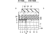
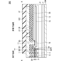
- FIG. 3 is a cross-sectional view taken along the line AA in FIG. 1 and schematically comprises a cell arrangement region CR, that is, an element region in which a semiconductor element is formed and a non-element region in which a semiconductor element is not formed. It is sectional drawing shown in.
- the configuration of the element region is the same as the configuration shown in FIG.
- a second well region 13 containing p-type impurities is provided in the upper layer of the drift layer 2, and the upper layer of the second well region 13 contains n-type impurities in a relatively high concentration.
- a p-type second well contact region 16 that is in contact with the second source region 15 and has a higher impurity concentration than the second well region 13 is selectively provided. ..
- the second source region 15 is formed in a size that occupies most of the upper layer portion of the second well region 13 in the plane direction, and the second well contact region 16 is the remaining portion of the upper layer portion of the second well region 13. Of these, it is provided closer to the element region than the second source region 15 and extends from the pn junction below the second source contact 17 (second contact) to below the boundary gate electrode 19. ing.
- the drift layer 2 between the first well region 3 adjacent to the second well region 13 and the second well region 13 is the outermost JFET region 14.
- the boundary between the element region and the non-element region is defined as the outermost JFET region 14.
- the field insulating film 28 is formed on the second well region 13, penetrates the field insulating film 28, and is electrically connected to the second source region 15 and the second well contact region 16.
- a second source contact 17 is provided.
- a boundary gate electrode 19 is provided on the second well region 13 and the first well region 3 at the boundary between the element region and the non-element region via the boundary gate insulating film 18. The boundary gate electrode 19 extends to the field insulating film 28 above the second source region 15.
- the gate electrode 9 in the element region and the boundary gate electrode 19 are discontinuous, but are continuous in a plan view.
- An interlayer insulating film 29 is provided on the drift layer 2 including the gate electrode 9 and the boundary gate electrode 19, and the gate electrode 9, the boundary gate electrode 19 and the source pad 101 are provided with an interlayer insulating film 29. It is electrically separated.
- the second source contact 17 also penetrates the interlayer insulating film 29 and is electrically connected to the second source region 15 and the second well contact region 16.
- a gate contact 27 is provided so as to penetrate the interlayer insulating film 29 and reach the boundary gate electrode 19 on the field insulating film 28, and the boundary gate electrode 19 and the gate electrode 9 pass through the gate contact 27. It is electrically connected to the gate wiring 103.
- a protective film PF is provided on the gate wiring 103 and the source pad 101 in the non-element region, and on a part of the source pad 101 in the element region.
- the protective film PF is composed of an insulating film.
- a silicide film SD composed of nickel silicide is provided at the bottom of the second source contact 17, and a part of the second source region 15 and the second well contact region 16 is covered with the silicide film SD.
- the second well contact region 16 and the second source region 15 are electrically connected to the source pad 101 via the silicide film SD and the second source contact 17.
- the silicide film SD is not limited to nickel silicide, and aluminum silicide and titanium silicide can also be used.
- the first source contact 7 can be formed by embedding a metal, for example, nickel, aluminum, or titanium, which is a material of the source pad 101, in the contact hole when the source pad 101 is formed.
- the impurity concentration of the second well region 13 is preferably 1.0 ⁇ 10 16 cm -3 or more and 1.0 ⁇ 10 20 cm -3 or less.
- the impurity concentration of the second source region 15 is preferably 1.0 ⁇ 10 17 cm -3 or more and 1.0 ⁇ 10 21 cm -3 or less.
- the impurity concentration of the second well contact region 16 is preferably 1.0 ⁇ 10 18 cm -3 or more and 1.0 ⁇ 10 22 cm -3 or less.
- the length of the second well contact region 16 extending from the lower pn junction of the second source contact 17 to the element region side is 1.0 ⁇ m or more and 100 ⁇ m or less. By setting it in such a range, it is possible to take a margin in the dimensional design of the silicon carbide semiconductor device.
- FIG. 4 is a cross-sectional view taken along the line BB in FIG. 1 and is a cross-sectional view schematically showing the configuration of an element region and a formation region of a gate pad 102 which is a non-element region. As shown in FIG. 4, the configurations of the element region and the non-element region are the same as those shown in FIG.
- FIG. 5 is a plan view schematically showing the configurations of the element region and the non-element region in the region X in FIG. 1.
- the insulating film and electrodes on the drift layer 2 are omitted, and only the configuration of the upper layer portion of the drift layer 2 is shown.
- the plan view shape of the unit cell UC in the element region is square and arranged in a matrix, but this is an example and is not limited to this shape, but is a rectangle. It can also be a polygon.
- the first source region 5 surrounds the first well contact region 6 having a square outer shape, and the outside thereof is surrounded by the first well region 3.
- the unit cell UCs are in the JFET region 4, and the corners between the unit cells UCs adjacent to each other in the diagonal direction are connected by the first well region 3.
- the second well contact region 16 is provided so as to be continuous with the second well contact region 13 and the second source region 15 is provided so as to be continuous with the second well contact region 16.
- the second well contact region 16 is continuously formed so as to extend below the plurality of second source contacts 17 in a plan view, and similarly, the second source region 15 is a plurality of second source contacts 17 in a plan view. It is continuously provided so as to extend below.
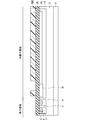
- FIG. 6 is a cross-sectional view taken along the line DD in FIG. 5 and is a cross-sectional view schematically showing the configuration of an element region and a non-element region.
- a plurality of second source contacts 17 are provided apart from each other, and between the plurality of second source contacts 17, as shown in FIG. 6, the boundary gate electrode 19 is an element region.
- the gate signal applied to the gate wiring 103 can be transmitted to the gate electrode 9 in the element region via the gate contact 27.
- FIGS. 7 to 18 are cross-sectional views showing the manufacturing process in order.
- the plane orientation of the first main surface is the (0001) plane, and the surface orientation is on the first main surface of the n-type low-resistance silicon carbide substrate 1 having a polytype of 4H.
- the n-type drift layer 2 of silicon carbide is epitaxially grown by a chemical vapor deposition (CVD) method.
- the concentration of n-type impurities in the drift layer 2 is, for example, 1 ⁇ 10 14 cm -3 to 1 ⁇ 10 17 cm -3, and the thickness of the drift layer 2 is, for example, 5 ⁇ m to 50 ⁇ m.
- an injection mask (not shown) is formed on the drift layer 2 by a photoresist or the like, and Al (aluminum), which is a p-type impurity, is ion-implanted into the upper layer of the drift layer 2 to form a p-type.
- the 1-well region 3 and the 2nd well region 13 are formed.
- the depth of ion implantation of Al is set to a depth that does not exceed the thickness of the drift layer 2, for example, 0.5 to 3 ⁇ m.
- the impurity concentration of the ion-implanted Al is, for example, 1 ⁇ 10 16 cm -3 to 1 ⁇ 10 20 cm -3 , which is higher than the n-type impurity concentration of the drift layer 2.
- the implantation mask is removed.
- the first well region 3 and the second well region 13 are formed in the same step, but they can also be formed in different steps.
- an injection mask (not shown) is formed on the drift layer 2 by a photoresist or the like, N (nitrogen), which is an n-type impurity, is ion-implanted, and the first well region 3 is formed.
- N nitrogen
- the n-type first source region 5 is formed in the upper layer portion
- the second source region 15 is formed in the upper layer portion of the second well region 13.
- the ion implantation depth of N is shallower than the thickness of the first well region 3 and the second well region 13.
- the impurity concentration of the ion-implanted N is, for example, 1 ⁇ 10 17 cm -3 to 1 ⁇ 10 21 cm -3 , which is higher than the p-type impurity concentration in the first well region 3 and the second well region 13, respectively. do.
- the implantation mask is removed.
- the first source region 5 and the second source region 15 are formed in the same step, but they can also be formed in separate steps.
- an injection mask (not shown) is formed on the drift layer 2 by a photoresist or the like, Al, which is a p-type impurity, is ion-implanted, and the upper layer portion of the first well region 3 is formed.
- the p-type first well contact region 6 is formed in the above, and the second well contact region 16 is formed in the upper layer of the second well region 13.
- the first well contact region 6 is formed at a depth that is electrically connected to the first well region 3 from the outermost surface of the first source region 5.
- the second well contact region 16 is formed at a depth that is electrically connected to the second well region 13 from the outermost surface of the second source region 15.
- the first well contact region 6 is provided in order to obtain good electrical contact between the first well region 3 and the first source contact 7 that electrically connects the source pad 101.
- the p-type impurity concentration in the first well contact region 6 and the second well contact region 16 is higher than the p-type impurity concentration in the first well region 3 and the second well contact region 13, respectively.
- the implantation mask is removed.
- the first well contact region 6 and the second well contact region 16 are formed in the same step, but they can also be formed in separate steps.
- an injection mask RM1 is formed on the drift layer 2 by a photoresist or the like, N, which is an n-type impurity, is ion-injected into the JFET region 4 and the outermost JFET region 14.
- N which is an n-type impurity
- the concentration of n-type impurities in the JFET region 4 and the outermost JFET region 14 is made higher than the concentration of n-type impurities in the drift layer 2.
- the impurity concentration of the ion-implanted N is lower than the p-type impurity concentration in the first well region 3.
- the impurities concentration in the JFET region 4 and the outermost JFET region 14 is relatively lower than that in the first well region 3, so that the first well region 3 and the JFET region 4 and the outermost JFET region 14 are separated from each other. This is to allow the depletion layer to extend to the JFET region 4 and the outermost JFET region 14 side when a reverse bias is applied to the pn junction formed between them.
- the injection mask RM1 is removed.
- the JFET region 4 and the outermost JFET region 14 having a higher impurity concentration than the drift layer 2 are formed by injecting n-type impurities, but the injection of n-type impurities is not always necessary. It is also possible to inject p-type impurities. Further, the impurity concentration in the JFET region 4 and the outermost JFET region 14 can be the same as the impurity concentration in the drift layer 2.
- an n-type or p-type epitaxial layer EP is epitaxially grown on the drift layer 2.
- the thickness of the epitaxial layer EP can be 10 to 500 nm.
- the epitaxial layer EP is provided as an epitaxial channel layer in which a channel is formed, but it is not an essential configuration and is not shown in FIGS. 2 to 4 and the figures shown below.
- the field insulating film 28 is formed on the drift layer 2 by the reduced pressure CVD method, and the etching mask RM2 is formed on the field insulating film 28 by a photoresist or the like. Then, the field insulating film 28 is partially etched and removed. The portion to be removed is a portion where the gate insulating film 8 and the boundary gate insulating film 18 are formed later. After that, the etching mask RM2 is removed.
- the surface of the drift layer 2 is thermally oxidized to form the gate insulating film 8 having a desired thickness.
- a polycrystalline silicon (polysilicon) film having conductivity is formed on the gate insulating film 8 by a reduced pressure CVD method, and the gate electrode 9 and the gate electrode 9 and the gate electrode 9 are patterned by etching.
- the boundary gate electrode 19 is formed. Further, the gate insulating film 8 not covered by the gate electrode 9 and the boundary gate electrode 19 is removed by etching or the like. Here, the gate insulating film 8 located below the boundary gate electrode 19 becomes the boundary gate insulating film 18.
- an interlayer insulating film 29 is formed on the drift layer 2 including the gate electrode 9 and the boundary gate electrode 19 by the reduced pressure CVD method.
- the second source contact hole 17C that penetrates the gate insulating film 8 and reaches the second well contact region 16 and the second source region 15 is formed.
- a gate contact hole 27C that penetrates the interlayer insulating film 29 and reaches the gate electrode 9 is formed.
- a metal film MF containing, for example, nickel (Ni) as a main component is formed on the interlayer insulating film 29 by a sputtering method or the like, and heat treatment is performed at a temperature of 600 ° C. or higher and 1100 ° C. or lower.
- a metal film MF containing Ni as a main component and silicon carbide are reacted to form a silicide film SD.
- the metal film MF remaining on the interlayer insulating film 29 other than the silicide film SD is removed by wet etching. Ohmic contact is formed on the bottom surfaces of the first source contact hole 7C and the second source contact hole 17C by the silicide film SD.
- a metal film containing Ni as a main component is formed on the second main surface (back surface) of the silicon carbide substrate 1, and the back surface is contacted with the back surface of the silicon carbide substrate 1 by heat treatment.
- a metal layer such as Al is formed on the front surface of the silicon carbide substrate 1 on which the interlayer insulating film 29 is formed by a sputtering method or a thin-film deposition method, and processed into a predetermined shape by a photolithography technique to form a first source contact. 7.
- the second source contact 17 and the gate contact 27 are formed, and the source pad 101 connected to the first source contact 7 and the second source contact 17 and the gate wiring 103 connected to the gate contact 27 are formed.
- the gate pad 102 (FIG. 4) connected to the gate wiring 103 is also formed. Further, a metal layer such as Al is formed on the back surface contact of the back surface of the silicon carbide substrate 1 by a sputtering method or a thin film deposition method to form a drain electrode 104. After that, by forming a protective film PF (FIG. 3) on the gate wiring 103 and the source pad 101 in the non-element region and a part of the upper part of the source pad 101 in the element region with an insulating film or the like, the n-type is formed. The silicon carbide MOSFET 100 is completed.
- the second well contact region 16 extends from the pn junction below the second source contact 17 to the element region side and extends to the element region side.
- Reference numeral 15 is provided so as to extend from the pn junction below the second source contact 17 toward the non-element region side.
- the second well contact region 16 is continuously formed so as to extend below the plurality of second source contacts 17 in a plan view, and similarly, the second source region 15 is formed. It is continuously provided so as to extend below the plurality of second source contacts 17 in a plan view. Therefore, when the n-type silicon carbide MOSFET 100 switches from the off state to the on state, the displacement current flowing in from the second source contact 17 can be dispersed, and the concentration of the displacement current can be avoided.
- the second source contact 17 is made of a metal such as nickel, aluminum, or titanium, and the bottom of the second source contact 17 is formed with a silicide film SD of silicon carbide and a metal to form a second source region 15 and a metal. Good ohmic contact is formed in both of the second well contact areas 16.
- the second source contact 17 and the second source contact 17 are formed.
- the contact resistance value (contact differential resistance value) per unit area with the 2-well contact region 16 is larger than the contact differential resistance value between the second source contact 17 and the second source region 15.
- the area of the second well contact region 16 below the second source contact 17 is made as large as possible. It is preferable to do so. Specifically, it is preferable that the area of the second well contact region 16 below the second source contact 17 is 1 to 100 times the area of the second source region 15 below the second source contact 17. Is.
- the impurity concentration in the second source region 15 is 1.0 ⁇ 10 17 cm -3 or more and 1.0 ⁇ 10 21 cm -3 or less, more preferably 1 ⁇ 10 19 cm -3 or more and 1 ⁇ 10 20 cm ⁇ . 3 or less.
- the impurity concentration in the second well contact region 16 is 1.0 ⁇ 10 18 cm -3 or more and 1.0 ⁇ 10 22 cm -3 or less, more preferably 1.0 ⁇ 10 19 cm -3 or more and 1.0. ⁇ 10 21 cm -3 or less.
- the sheet resistance value of the second source region 15 is lower than the sheet resistance value of the second well contact region 16. This facilitates the flow of current in the second source region 15.
- the n-type silicon carbide MOSFET 100 switches from the off state to the on state, for example, between a large dV / dt (time fluctuation of voltage) source of 20 V / n sec or more and a drain.
- a larger proportion of the displacement current flowing in from the second source contact 17 can flow through the second source region to the non-element region side of the second source contact 17 and to the second. It is possible to suppress the displacement current flowing toward the element region side of the source contact 17. Therefore, the voltage generated at the end of the second well region 13 on the element region side (the end of the second well region 13) can be reduced, and the voltage between the end of the second well region 13 and the boundary gate electrode 19 can be reduced. The potential difference is suppressed, the dielectric breakdown of the boundary gate insulating film 18 is suppressed, and the reliability as a semiconductor device is improved.
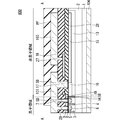
- FIG. 19 is a cross-sectional view showing the configuration of the n-type silicon carbide MOSFET 200 according to the second embodiment, and corresponds to the cross-sectional view taken along the line AA in FIG.
- the portion extending from the pn junction below the second source contact 17 of the second well contact region 16 toward the element region is directly below the field insulating film 28. It extends only to, and does not reach directly below the boundary gate electrode 19.
- FIG. 20 is a cross-sectional view taken along the line BB in FIG. 1 and is a cross-sectional view schematically showing the configuration of an element region and a formation region of a gate pad 102 which is a non-element region. As shown in FIG. 20, the configuration of the element region and the non-element region is the same as the configuration shown in FIG.
- the boundary portion is on the second well contact region 16 having a high concentration.
- the gate insulating film 18 is not formed, and the film quality of the boundary gate insulating film 18 is improved. That is, since the crystal structure is broken in the high-concentration impurity injection region, the homogeneity of the boundary gate insulating film 18 formed on the crystal structure is deteriorated, but this occurs in the configuration of the n-type silicon carbide MOSFET 200. However, the film quality evaluated by withstand voltage and leakage current is improved. Therefore, the effect of suppressing the dielectric breakdown of the boundary gate insulating film 18 becomes higher, and the reliability as a semiconductor device is further improved.
- FIG. 21 is a plan view showing the configuration of the element region and the non-element region of the n-type silicon carbide MOSFET 300 of the third embodiment, and corresponds to the plan view of the region X in FIG.
- the insulating film and electrodes on the drift layer 2 are omitted, and only the configuration of the upper layer portion of the drift layer 2 is shown.
- the same components as those described with reference to FIG. 5 are designated by the same reference numerals, and duplicate description will be omitted.
- the length of the portion extending from the junction with the second source region 15 to the element region side is the second. 2 It is shorter than the length of the portion extending from the lower pn junction of the source contact 17 to the element region side. Then, the length of the second source region 15 is formed longer by the amount that the length of the second well contact region 16 is shortened.
- the second well contact region 16 is partially recessed toward the element region, and the second source region 15 is partially projected.
- the second well contact region 16 is recessed and the second source region 15 is projected at only one portion between the two second source contacts 17, but typically. Since a plurality of second source contacts 17 are provided along the gate wiring 103 in the non-elemental region, the second well contact region 16 is recessed between the second source contacts 17, and the portion where the second source region 15 protrudes is formed. Can be provided.
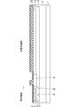
- FIG. 22 is a cross-sectional view taken along the line DD in FIG. 21 in the direction indicated by the arrow.
- the length of the second well contact region 16 is the element region from the junction with the second source region 15 of the n-type silicon carbide MOSFET 100 shown in FIG.
- the second well contact region 16 extending to the side is formed shorter than the length, and the second source region 15 is formed longer by that amount.
- the second source is used when the n-type silicon carbide MOSFET 300 switches from the off state to the on state.
- a larger percentage of the displacement current flowing in from the contact 17 can flow through the lengthened second source region 15 towards the non-device region more than the second source contact 17 and more than the second source contact 17.
- the displacement current flowing on the element region side can be further suppressed. Therefore, the voltage generated at the end of the second well region 13 on the element region side (the end of the second well region 13) can be further reduced, and between the end of the second well region 13 and the boundary gate electrode 19.
- the potential difference between the two is further suppressed, the effect of suppressing the dielectric breakdown of the boundary gate insulating film 18 is further enhanced, and the reliability as a semiconductor device is further improved.
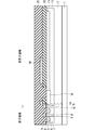
- FIG. 23 is a cross-sectional view showing the configuration of the n-type silicon carbide MOSFET 400 according to the fourth embodiment, and corresponds to the cross-sectional view taken along the line AA in FIG.
- the portion extending from the pn junction below the second source contact 17 of the second well contact region 16 toward the element region is the portion of the second well contact region 13. It is provided up to the end (the 13th end of the second well region).
- FIG. 24 is a cross-sectional view taken along the line BB in FIG. 1 and is a cross-sectional view schematically showing the configuration of an element region and a formation region of a gate pad 102 which is a non-element region. As shown in FIG. 24, the configuration of the element region and the non-element region is the same as the configuration shown in FIG. 23.
- the n-type silicon carbide MOSFET 400 of the fourth embodiment since the second well contact region 16 is provided up to the end of the second well region 13, the n-type silicon carbide MOSFET 400 switches from the off state to the on state. At the same time, the voltage generated at the end of the second well region 13 can be effectively reduced.
- the sheet resistance value of the second well contact region 16 is lower than the sheet resistance of the second well contact region 13
- the voltage generated at the end of the second well contact region 16 is generated at the end of the second well region 13. It can be lower than the voltage to be applied.
- the potential difference between the end of the second well region 13 and the boundary gate electrode 19 is further suppressed, the effect of suppressing dielectric breakdown of the boundary gate insulating film 18 is further increased, and the reliability as a semiconductor device is further increased. improves.
- each embodiment can be freely combined, and each embodiment can be appropriately modified or omitted within the scope of the disclosure.
Landscapes
- Electrodes Of Semiconductors (AREA)
Priority Applications (5)
| Application Number | Priority Date | Filing Date | Title |
|---|---|---|---|
| CN202080100712.4A CN115917755B (zh) | 2020-06-24 | 2020-06-24 | 碳化硅半导体装置 |
| DE112020007341.6T DE112020007341T5 (de) | 2020-06-24 | 2020-06-24 | Siliciumcarbid-halbleitereinheit |
| PCT/JP2020/024835 WO2021260853A1 (ja) | 2020-06-24 | 2020-06-24 | 炭化珪素半導体装置 |
| US17/917,564 US12279447B2 (en) | 2020-06-24 | 2020-06-24 | Silicon carbide semiconductor device |
| JP2020553681A JP6840300B1 (ja) | 2020-06-24 | 2020-06-24 | 炭化珪素半導体装置 |
Applications Claiming Priority (1)
| Application Number | Priority Date | Filing Date | Title |
|---|---|---|---|
| PCT/JP2020/024835 WO2021260853A1 (ja) | 2020-06-24 | 2020-06-24 | 炭化珪素半導体装置 |
Publications (1)
| Publication Number | Publication Date |
|---|---|
| WO2021260853A1 true WO2021260853A1 (ja) | 2021-12-30 |
Family
ID=74845352
Family Applications (1)
| Application Number | Title | Priority Date | Filing Date |
|---|---|---|---|
| PCT/JP2020/024835 Ceased WO2021260853A1 (ja) | 2020-06-24 | 2020-06-24 | 炭化珪素半導体装置 |
Country Status (5)
| Country | Link |
|---|---|
| US (1) | US12279447B2 (https=) |
| JP (1) | JP6840300B1 (https=) |
| CN (1) | CN115917755B (https=) |
| DE (1) | DE112020007341T5 (https=) |
| WO (1) | WO2021260853A1 (https=) |
Families Citing this family (1)
| Publication number | Priority date | Publication date | Assignee | Title |
|---|---|---|---|---|
| CN117693824A (zh) * | 2021-09-15 | 2024-03-12 | 住友电气工业株式会社 | 碳化硅半导体器件 |
Citations (3)
| Publication number | Priority date | Publication date | Assignee | Title |
|---|---|---|---|---|
| JP2005116951A (ja) * | 2003-10-10 | 2005-04-28 | Toyota Central Res & Dev Lab Inc | 半導体装置 |
| JP2014150279A (ja) * | 2009-02-24 | 2014-08-21 | Mitsubishi Electric Corp | 炭化珪素半導体装置 |
| WO2016147352A1 (ja) * | 2015-03-18 | 2016-09-22 | 三菱電機株式会社 | 電力用半導体装置 |
Family Cites Families (10)
| Publication number | Priority date | Publication date | Assignee | Title |
|---|---|---|---|---|
| JP4432332B2 (ja) | 2003-03-06 | 2010-03-17 | サンケン電気株式会社 | 半導体素子及びその製造方法 |
| CN102473723B (zh) * | 2009-07-15 | 2014-12-03 | 三菱电机株式会社 | 功率用半导体装置及其制造方法 |
| JP5321377B2 (ja) | 2009-09-11 | 2013-10-23 | 三菱電機株式会社 | 電力用半導体装置 |
| JP4962665B2 (ja) | 2010-04-06 | 2012-06-27 | 三菱電機株式会社 | 電力用半導体装置およびその製造方法、ならびにパワーモジュール |
| DE112014006726T5 (de) * | 2014-08-08 | 2017-03-23 | Hitachi, Ltd. | Halbleitervorrichtung, Leistungsmodul, Stromrichtvorrichtung, Fahrzeug und Schienenfahrzeug |
| JP6058228B1 (ja) * | 2015-04-22 | 2017-01-11 | 三菱電機株式会社 | 半導体装置および半導体装置の製造方法 |
| JP6580270B2 (ja) * | 2016-08-25 | 2019-09-25 | 三菱電機株式会社 | 炭化珪素半導体装置 |
| WO2018055719A1 (ja) * | 2016-09-23 | 2018-03-29 | 三菱電機株式会社 | 炭化珪素半導体装置 |
| DE112018006467B4 (de) * | 2017-12-19 | 2022-11-17 | Mitsubishi Electric Corporation | Siliciumcarbid-halbleiteranordnung und leistungswandler |
| DE112019007188B4 (de) * | 2019-04-11 | 2025-10-16 | Mitsubishi Electric Corporation | Halbleitereinheit und leistungswandlereinheit |
-
2020
- 2020-06-24 DE DE112020007341.6T patent/DE112020007341T5/de active Pending
- 2020-06-24 CN CN202080100712.4A patent/CN115917755B/zh active Active
- 2020-06-24 JP JP2020553681A patent/JP6840300B1/ja active Active
- 2020-06-24 WO PCT/JP2020/024835 patent/WO2021260853A1/ja not_active Ceased
- 2020-06-24 US US17/917,564 patent/US12279447B2/en active Active
Patent Citations (3)
| Publication number | Priority date | Publication date | Assignee | Title |
|---|---|---|---|---|
| JP2005116951A (ja) * | 2003-10-10 | 2005-04-28 | Toyota Central Res & Dev Lab Inc | 半導体装置 |
| JP2014150279A (ja) * | 2009-02-24 | 2014-08-21 | Mitsubishi Electric Corp | 炭化珪素半導体装置 |
| WO2016147352A1 (ja) * | 2015-03-18 | 2016-09-22 | 三菱電機株式会社 | 電力用半導体装置 |
Also Published As
| Publication number | Publication date |
|---|---|
| US12279447B2 (en) | 2025-04-15 |
| DE112020007341T5 (de) | 2023-04-06 |
| CN115917755B (zh) | 2025-08-01 |
| US20230155021A1 (en) | 2023-05-18 |
| JP6840300B1 (ja) | 2021-03-10 |
| JPWO2021260853A1 (https=) | 2021-12-30 |
| CN115917755A (zh) | 2023-04-04 |
Similar Documents
| Publication | Publication Date | Title |
|---|---|---|
| JP7786512B2 (ja) | 半導体装置 | |
| JP4153811B2 (ja) | 高耐圧半導体装置及びその製造方法 | |
| US7791135B2 (en) | Insulated gate silicon carbide semiconductor device and method for manufacturing the same | |
| KR102531554B1 (ko) | 실리콘카바이드 트랜지스터 및 이의 제조방법 | |
| US6855970B2 (en) | High-breakdown-voltage semiconductor device | |
| JP3721172B2 (ja) | 半導体装置 | |
| JP7643621B2 (ja) | 半導体装置 | |
| JP7390984B2 (ja) | 半導体装置 | |
| JP2008177335A (ja) | 炭化珪素絶縁ゲート型半導体装置。 | |
| JP7158317B2 (ja) | 半導体装置 | |
| JPH08181313A (ja) | 横型トレンチmisfetおよびその製造方法 | |
| CN103972292A (zh) | 半导体装置及其制造方法 | |
| WO2014083771A1 (ja) | 半導体素子及びその製造方法 | |
| KR101875638B1 (ko) | 반도체 소자 및 그 제조 방법 | |
| JP2023060183A (ja) | 半導体装置 | |
| TW202406139A (zh) | 半導體裝置及其製造方法 | |
| JP6840300B1 (ja) | 炭化珪素半導体装置 | |
| JP4948784B2 (ja) | 半導体装置及びその製造方法 | |
| TWI488307B (zh) | Power transistor structure and manufacturing method | |
| JP2013055177A (ja) | 半導体装置及びその製造方法 | |
| JP7643179B2 (ja) | 炭化珪素半導体装置 | |
| JP7647087B2 (ja) | 半導体装置 | |
| JP7731660B2 (ja) | 半導体装置および半導体装置の製造方法 | |
| US12495562B2 (en) | Semiconductor device and fabrication method thereof | |
| JP7752780B2 (ja) | 半導体装置およびその製造方法 |
Legal Events
| Date | Code | Title | Description |
|---|---|---|---|
| ENP | Entry into the national phase |
Ref document number: 2020553681 Country of ref document: JP Kind code of ref document: A |
|
| 121 | Ep: the epo has been informed by wipo that ep was designated in this application |
Ref document number: 20942359 Country of ref document: EP Kind code of ref document: A1 |
|
| 122 | Ep: pct application non-entry in european phase |
Ref document number: 20942359 Country of ref document: EP Kind code of ref document: A1 |
|
| WWG | Wipo information: grant in national office |
Ref document number: 17917564 Country of ref document: US |
|
| WWG | Wipo information: grant in national office |
Ref document number: 202080100712.4 Country of ref document: CN |