WO2021260853A1 - 炭化珪素半導体装置 - Google Patents
炭化珪素半導体装置 Download PDFInfo
- Publication number
- WO2021260853A1 WO2021260853A1 PCT/JP2020/024835 JP2020024835W WO2021260853A1 WO 2021260853 A1 WO2021260853 A1 WO 2021260853A1 JP 2020024835 W JP2020024835 W JP 2020024835W WO 2021260853 A1 WO2021260853 A1 WO 2021260853A1
- Authority
- WO
- WIPO (PCT)
- Prior art keywords
- region
- contact
- well
- silicon carbide
- semiconductor device
- Prior art date
Links
- HBMJWWWQQXIZIP-UHFFFAOYSA-N silicon carbide Chemical compound [Si+]#[C-] HBMJWWWQQXIZIP-UHFFFAOYSA-N 0.000 title claims abstract description 96
- 229910010271 silicon carbide Inorganic materials 0.000 title claims abstract description 96
- 239000004065 semiconductor Substances 0.000 title claims abstract description 85
- 239000012535 impurity Substances 0.000 claims abstract description 88
- 239000000758 substrate Substances 0.000 claims description 15
- 239000010408 film Substances 0.000 description 86
- 239000010410 layer Substances 0.000 description 73
- 238000004519 manufacturing process Methods 0.000 description 17
- 238000006073 displacement reaction Methods 0.000 description 16
- 239000011229 interlayer Substances 0.000 description 12
- 229910052751 metal Inorganic materials 0.000 description 12
- 239000002184 metal Substances 0.000 description 12
- 229910021332 silicide Inorganic materials 0.000 description 12
- FVBUAEGBCNSCDD-UHFFFAOYSA-N silicide(4-) Chemical compound [Si-4] FVBUAEGBCNSCDD-UHFFFAOYSA-N 0.000 description 12
- PXHVJJICTQNCMI-UHFFFAOYSA-N Nickel Chemical compound [Ni] PXHVJJICTQNCMI-UHFFFAOYSA-N 0.000 description 11
- 239000000463 material Substances 0.000 description 8
- 238000002347 injection Methods 0.000 description 7
- 239000007924 injection Substances 0.000 description 7
- 230000015556 catabolic process Effects 0.000 description 6
- 238000005468 ion implantation Methods 0.000 description 6
- 238000005229 chemical vapour deposition Methods 0.000 description 5
- 230000000694 effects Effects 0.000 description 5
- 238000000034 method Methods 0.000 description 5
- 229920002120 photoresistant polymer Polymers 0.000 description 5
- 229910052782 aluminium Inorganic materials 0.000 description 4
- XAGFODPZIPBFFR-UHFFFAOYSA-N aluminium Chemical compound [Al] XAGFODPZIPBFFR-UHFFFAOYSA-N 0.000 description 4
- 230000015572 biosynthetic process Effects 0.000 description 4
- 230000005684 electric field Effects 0.000 description 4
- 238000005530 etching Methods 0.000 description 4
- 229910052759 nickel Inorganic materials 0.000 description 4
- RUFLMLWJRZAWLJ-UHFFFAOYSA-N nickel silicide Chemical compound [Ni]=[Si]=[Ni] RUFLMLWJRZAWLJ-UHFFFAOYSA-N 0.000 description 4
- 229910021334 nickel silicide Inorganic materials 0.000 description 4
- RTAQQCXQSZGOHL-UHFFFAOYSA-N Titanium Chemical compound [Ti] RTAQQCXQSZGOHL-UHFFFAOYSA-N 0.000 description 3
- 230000005669 field effect Effects 0.000 description 3
- 238000002513 implantation Methods 0.000 description 3
- 229910021420 polycrystalline silicon Inorganic materials 0.000 description 3
- 230000001681 protective effect Effects 0.000 description 3
- 238000004544 sputter deposition Methods 0.000 description 3
- 239000010936 titanium Substances 0.000 description 3
- 229910052719 titanium Inorganic materials 0.000 description 3
- IJGRMHOSHXDMSA-UHFFFAOYSA-N Atomic nitrogen Chemical compound N#N IJGRMHOSHXDMSA-UHFFFAOYSA-N 0.000 description 2
- LKTZODAHLMBGLG-UHFFFAOYSA-N alumanylidynesilicon;$l^{2}-alumanylidenesilylidenealuminum Chemical compound [Si]#[Al].[Si]#[Al].[Al]=[Si]=[Al] LKTZODAHLMBGLG-UHFFFAOYSA-N 0.000 description 2
- 239000013078 crystal Substances 0.000 description 2
- -1 for example Substances 0.000 description 2
- 238000010438 heat treatment Methods 0.000 description 2
- 229910044991 metal oxide Inorganic materials 0.000 description 2
- 150000004706 metal oxides Chemical class 0.000 description 2
- 230000000149 penetrating effect Effects 0.000 description 2
- 238000009751 slip forming Methods 0.000 description 2
- 238000007736 thin film deposition technique Methods 0.000 description 2
- 229910021341 titanium silicide Inorganic materials 0.000 description 2
- XUIMIQQOPSSXEZ-UHFFFAOYSA-N Silicon Chemical compound [Si] XUIMIQQOPSSXEZ-UHFFFAOYSA-N 0.000 description 1
- 238000005516 engineering process Methods 0.000 description 1
- 230000010354 integration Effects 0.000 description 1
- 150000002500 ions Chemical class 0.000 description 1
- 239000011159 matrix material Substances 0.000 description 1
- 229910052757 nitrogen Inorganic materials 0.000 description 1
- 230000003071 parasitic effect Effects 0.000 description 1
- 238000000206 photolithography Methods 0.000 description 1
- 229920005591 polysilicon Polymers 0.000 description 1
- 238000004904 shortening Methods 0.000 description 1
- 229910052710 silicon Inorganic materials 0.000 description 1
- 239000010703 silicon Substances 0.000 description 1
- 238000001039 wet etching Methods 0.000 description 1
Images


Classifications
-
- H—ELECTRICITY
- H01—ELECTRIC ELEMENTS
- H01L—SEMICONDUCTOR DEVICES NOT COVERED BY CLASS H10
- H01L29/00—Semiconductor devices specially adapted for rectifying, amplifying, oscillating or switching and having potential barriers; Capacitors or resistors having potential barriers, e.g. a PN-junction depletion layer or carrier concentration layer; Details of semiconductor bodies or of electrodes thereof ; Multistep manufacturing processes therefor
- H01L29/66—Types of semiconductor device ; Multistep manufacturing processes therefor
- H01L29/68—Types of semiconductor device ; Multistep manufacturing processes therefor controllable by only the electric current supplied, or only the electric potential applied, to an electrode which does not carry the current to be rectified, amplified or switched
- H01L29/76—Unipolar devices, e.g. field effect transistors
- H01L29/772—Field effect transistors
- H01L29/78—Field effect transistors with field effect produced by an insulated gate
- H01L29/7801—DMOS transistors, i.e. MISFETs with a channel accommodating body or base region adjoining a drain drift region
- H01L29/7802—Vertical DMOS transistors, i.e. VDMOS transistors
- H01L29/7811—Vertical DMOS transistors, i.e. VDMOS transistors with an edge termination structure
-
- H—ELECTRICITY
- H01—ELECTRIC ELEMENTS
- H01L—SEMICONDUCTOR DEVICES NOT COVERED BY CLASS H10
- H01L29/00—Semiconductor devices specially adapted for rectifying, amplifying, oscillating or switching and having potential barriers; Capacitors or resistors having potential barriers, e.g. a PN-junction depletion layer or carrier concentration layer; Details of semiconductor bodies or of electrodes thereof ; Multistep manufacturing processes therefor
- H01L29/02—Semiconductor bodies ; Multistep manufacturing processes therefor
- H01L29/06—Semiconductor bodies ; Multistep manufacturing processes therefor characterised by their shape; characterised by the shapes, relative sizes, or dispositions of the semiconductor regions ; characterised by the concentration or distribution of impurities within semiconductor regions
- H01L29/0684—Semiconductor bodies ; Multistep manufacturing processes therefor characterised by their shape; characterised by the shapes, relative sizes, or dispositions of the semiconductor regions ; characterised by the concentration or distribution of impurities within semiconductor regions characterised by the shape, relative sizes or dispositions of the semiconductor regions or junctions between the regions
- H01L29/0692—Surface layout
- H01L29/0696—Surface layout of cellular field-effect devices, e.g. multicellular DMOS transistors or IGBTs
-
- H—ELECTRICITY
- H01—ELECTRIC ELEMENTS
- H01L—SEMICONDUCTOR DEVICES NOT COVERED BY CLASS H10
- H01L29/00—Semiconductor devices specially adapted for rectifying, amplifying, oscillating or switching and having potential barriers; Capacitors or resistors having potential barriers, e.g. a PN-junction depletion layer or carrier concentration layer; Details of semiconductor bodies or of electrodes thereof ; Multistep manufacturing processes therefor
- H01L29/02—Semiconductor bodies ; Multistep manufacturing processes therefor
- H01L29/06—Semiconductor bodies ; Multistep manufacturing processes therefor characterised by their shape; characterised by the shapes, relative sizes, or dispositions of the semiconductor regions ; characterised by the concentration or distribution of impurities within semiconductor regions
- H01L29/08—Semiconductor bodies ; Multistep manufacturing processes therefor characterised by their shape; characterised by the shapes, relative sizes, or dispositions of the semiconductor regions ; characterised by the concentration or distribution of impurities within semiconductor regions with semiconductor regions connected to an electrode carrying current to be rectified, amplified or switched and such electrode being part of a semiconductor device which comprises three or more electrodes
- H01L29/0843—Source or drain regions of field-effect devices
- H01L29/0847—Source or drain regions of field-effect devices of field-effect transistors with insulated gate
- H01L29/0852—Source or drain regions of field-effect devices of field-effect transistors with insulated gate of DMOS transistors
- H01L29/0856—Source regions
- H01L29/086—Impurity concentration or distribution
-
- H—ELECTRICITY
- H01—ELECTRIC ELEMENTS
- H01L—SEMICONDUCTOR DEVICES NOT COVERED BY CLASS H10
- H01L29/00—Semiconductor devices specially adapted for rectifying, amplifying, oscillating or switching and having potential barriers; Capacitors or resistors having potential barriers, e.g. a PN-junction depletion layer or carrier concentration layer; Details of semiconductor bodies or of electrodes thereof ; Multistep manufacturing processes therefor
- H01L29/02—Semiconductor bodies ; Multistep manufacturing processes therefor
- H01L29/12—Semiconductor bodies ; Multistep manufacturing processes therefor characterised by the materials of which they are formed
- H01L29/16—Semiconductor bodies ; Multistep manufacturing processes therefor characterised by the materials of which they are formed including, apart from doping materials or other impurities, only elements of Group IV of the Periodic Table
- H01L29/1608—Silicon carbide
-
- H—ELECTRICITY
- H01—ELECTRIC ELEMENTS
- H01L—SEMICONDUCTOR DEVICES NOT COVERED BY CLASS H10
- H01L29/00—Semiconductor devices specially adapted for rectifying, amplifying, oscillating or switching and having potential barriers; Capacitors or resistors having potential barriers, e.g. a PN-junction depletion layer or carrier concentration layer; Details of semiconductor bodies or of electrodes thereof ; Multistep manufacturing processes therefor
- H01L29/40—Electrodes ; Multistep manufacturing processes therefor
- H01L29/41—Electrodes ; Multistep manufacturing processes therefor characterised by their shape, relative sizes or dispositions
- H01L29/417—Electrodes ; Multistep manufacturing processes therefor characterised by their shape, relative sizes or dispositions carrying the current to be rectified, amplified or switched
- H01L29/41725—Source or drain electrodes for field effect devices
- H01L29/41741—Source or drain electrodes for field effect devices for vertical or pseudo-vertical devices
-
- H—ELECTRICITY
- H01—ELECTRIC ELEMENTS
- H01L—SEMICONDUCTOR DEVICES NOT COVERED BY CLASS H10
- H01L29/00—Semiconductor devices specially adapted for rectifying, amplifying, oscillating or switching and having potential barriers; Capacitors or resistors having potential barriers, e.g. a PN-junction depletion layer or carrier concentration layer; Details of semiconductor bodies or of electrodes thereof ; Multistep manufacturing processes therefor
- H01L29/40—Electrodes ; Multistep manufacturing processes therefor
- H01L29/41—Electrodes ; Multistep manufacturing processes therefor characterised by their shape, relative sizes or dispositions
- H01L29/417—Electrodes ; Multistep manufacturing processes therefor characterised by their shape, relative sizes or dispositions carrying the current to be rectified, amplified or switched
- H01L29/41725—Source or drain electrodes for field effect devices
- H01L29/41775—Source or drain electrodes for field effect devices characterised by the proximity or the relative position of the source or drain electrode and the gate electrode, e.g. the source or drain electrode separated from the gate electrode by side-walls or spreading around or above the gate electrode
- H01L29/41783—Raised source or drain electrodes self aligned with the gate
-
- H—ELECTRICITY
- H01—ELECTRIC ELEMENTS
- H01L—SEMICONDUCTOR DEVICES NOT COVERED BY CLASS H10
- H01L29/00—Semiconductor devices specially adapted for rectifying, amplifying, oscillating or switching and having potential barriers; Capacitors or resistors having potential barriers, e.g. a PN-junction depletion layer or carrier concentration layer; Details of semiconductor bodies or of electrodes thereof ; Multistep manufacturing processes therefor
- H01L29/40—Electrodes ; Multistep manufacturing processes therefor
- H01L29/41—Electrodes ; Multistep manufacturing processes therefor characterised by their shape, relative sizes or dispositions
- H01L29/423—Electrodes ; Multistep manufacturing processes therefor characterised by their shape, relative sizes or dispositions not carrying the current to be rectified, amplified or switched
- H01L29/42312—Gate electrodes for field effect devices
- H01L29/42316—Gate electrodes for field effect devices for field-effect transistors
- H01L29/4232—Gate electrodes for field effect devices for field-effect transistors with insulated gate
- H01L29/42356—Disposition, e.g. buried gate electrode
-
- H—ELECTRICITY
- H01—ELECTRIC ELEMENTS
- H01L—SEMICONDUCTOR DEVICES NOT COVERED BY CLASS H10
- H01L29/00—Semiconductor devices specially adapted for rectifying, amplifying, oscillating or switching and having potential barriers; Capacitors or resistors having potential barriers, e.g. a PN-junction depletion layer or carrier concentration layer; Details of semiconductor bodies or of electrodes thereof ; Multistep manufacturing processes therefor
- H01L29/66—Types of semiconductor device ; Multistep manufacturing processes therefor
- H01L29/66007—Multistep manufacturing processes
- H01L29/66053—Multistep manufacturing processes of devices having a semiconductor body comprising crystalline silicon carbide
- H01L29/66068—Multistep manufacturing processes of devices having a semiconductor body comprising crystalline silicon carbide the devices being controllable only by the electric current supplied or the electric potential applied, to an electrode which does not carry the current to be rectified, amplified or switched, e.g. three-terminal devices
-
- H—ELECTRICITY
- H01—ELECTRIC ELEMENTS
- H01L—SEMICONDUCTOR DEVICES NOT COVERED BY CLASS H10
- H01L29/00—Semiconductor devices specially adapted for rectifying, amplifying, oscillating or switching and having potential barriers; Capacitors or resistors having potential barriers, e.g. a PN-junction depletion layer or carrier concentration layer; Details of semiconductor bodies or of electrodes thereof ; Multistep manufacturing processes therefor
- H01L29/02—Semiconductor bodies ; Multistep manufacturing processes therefor
- H01L29/06—Semiconductor bodies ; Multistep manufacturing processes therefor characterised by their shape; characterised by the shapes, relative sizes, or dispositions of the semiconductor regions ; characterised by the concentration or distribution of impurities within semiconductor regions
- H01L29/0603—Semiconductor bodies ; Multistep manufacturing processes therefor characterised by their shape; characterised by the shapes, relative sizes, or dispositions of the semiconductor regions ; characterised by the concentration or distribution of impurities within semiconductor regions characterised by particular constructional design considerations, e.g. for preventing surface leakage, for controlling electric field concentration or for internal isolations regions
- H01L29/0607—Semiconductor bodies ; Multistep manufacturing processes therefor characterised by their shape; characterised by the shapes, relative sizes, or dispositions of the semiconductor regions ; characterised by the concentration or distribution of impurities within semiconductor regions characterised by particular constructional design considerations, e.g. for preventing surface leakage, for controlling electric field concentration or for internal isolations regions for preventing surface leakage or controlling electric field concentration
- H01L29/0611—Semiconductor bodies ; Multistep manufacturing processes therefor characterised by their shape; characterised by the shapes, relative sizes, or dispositions of the semiconductor regions ; characterised by the concentration or distribution of impurities within semiconductor regions characterised by particular constructional design considerations, e.g. for preventing surface leakage, for controlling electric field concentration or for internal isolations regions for preventing surface leakage or controlling electric field concentration for increasing or controlling the breakdown voltage of reverse biased devices
- H01L29/0615—Semiconductor bodies ; Multistep manufacturing processes therefor characterised by their shape; characterised by the shapes, relative sizes, or dispositions of the semiconductor regions ; characterised by the concentration or distribution of impurities within semiconductor regions characterised by particular constructional design considerations, e.g. for preventing surface leakage, for controlling electric field concentration or for internal isolations regions for preventing surface leakage or controlling electric field concentration for increasing or controlling the breakdown voltage of reverse biased devices by the doping profile or the shape or the arrangement of the PN junction, or with supplementary regions, e.g. junction termination extension [JTE]
- H01L29/0619—Semiconductor bodies ; Multistep manufacturing processes therefor characterised by their shape; characterised by the shapes, relative sizes, or dispositions of the semiconductor regions ; characterised by the concentration or distribution of impurities within semiconductor regions characterised by particular constructional design considerations, e.g. for preventing surface leakage, for controlling electric field concentration or for internal isolations regions for preventing surface leakage or controlling electric field concentration for increasing or controlling the breakdown voltage of reverse biased devices by the doping profile or the shape or the arrangement of the PN junction, or with supplementary regions, e.g. junction termination extension [JTE] with a supplementary region doped oppositely to or in rectifying contact with the semiconductor containing or contacting region, e.g. guard rings with PN or Schottky junction
-
- H—ELECTRICITY
- H01—ELECTRIC ELEMENTS
- H01L—SEMICONDUCTOR DEVICES NOT COVERED BY CLASS H10
- H01L29/00—Semiconductor devices specially adapted for rectifying, amplifying, oscillating or switching and having potential barriers; Capacitors or resistors having potential barriers, e.g. a PN-junction depletion layer or carrier concentration layer; Details of semiconductor bodies or of electrodes thereof ; Multistep manufacturing processes therefor
- H01L29/40—Electrodes ; Multistep manufacturing processes therefor
- H01L29/41—Electrodes ; Multistep manufacturing processes therefor characterised by their shape, relative sizes or dispositions
- H01L29/423—Electrodes ; Multistep manufacturing processes therefor characterised by their shape, relative sizes or dispositions not carrying the current to be rectified, amplified or switched
- H01L29/42312—Gate electrodes for field effect devices
- H01L29/42316—Gate electrodes for field effect devices for field-effect transistors
- H01L29/4232—Gate electrodes for field effect devices for field-effect transistors with insulated gate
- H01L29/42372—Gate electrodes for field effect devices for field-effect transistors with insulated gate characterised by the conducting layer, e.g. the length, the sectional shape or the lay-out
- H01L29/4238—Gate electrodes for field effect devices for field-effect transistors with insulated gate characterised by the conducting layer, e.g. the length, the sectional shape or the lay-out characterised by the surface lay-out
-
- H—ELECTRICITY
- H01—ELECTRIC ELEMENTS
- H01L—SEMICONDUCTOR DEVICES NOT COVERED BY CLASS H10
- H01L29/00—Semiconductor devices specially adapted for rectifying, amplifying, oscillating or switching and having potential barriers; Capacitors or resistors having potential barriers, e.g. a PN-junction depletion layer or carrier concentration layer; Details of semiconductor bodies or of electrodes thereof ; Multistep manufacturing processes therefor
- H01L29/66—Types of semiconductor device ; Multistep manufacturing processes therefor
- H01L29/68—Types of semiconductor device ; Multistep manufacturing processes therefor controllable by only the electric current supplied, or only the electric potential applied, to an electrode which does not carry the current to be rectified, amplified or switched
- H01L29/70—Bipolar devices
- H01L29/72—Transistor-type devices, i.e. able to continuously respond to applied control signals
- H01L29/739—Transistor-type devices, i.e. able to continuously respond to applied control signals controlled by field-effect, e.g. bipolar static induction transistors [BSIT]
- H01L29/7393—Insulated gate bipolar mode transistors, i.e. IGBT; IGT; COMFET
- H01L29/7395—Vertical transistors, e.g. vertical IGBT
Definitions
- the present disclosure relates to a silicon carbide semiconductor device, and more particularly to a silicon carbide semiconductor device having a gate insulating film.
- MOS Metal Oxide Semiconductor
- IGBT Insulated Gate Bipolar Transistor
- MOSFET Metal Oxide Semiconductor Field Effect Transistor
- the n-type MOSFET which is one of the silicon carbide semiconductor devices using silicon carbide having a bandgap about three times larger than the bandgap of silicon (Si) as a semiconductor material, is an inverter by using it as a switching element of an inverter circuit. The power loss of the circuit can be reduced.
- the n-type MOSFET typically has an n-type drift layer and a p-type well provided on the n-type drift layer, and when the MOSFET is switched from the on state to the off state, the drain voltage of the MOSFET is generated. That is, the voltage of the drain electrode rises sharply and changes from about 0 V to several hundred V. Then, a displacement current is generated through the parasitic capacitance existing between the p-type well and the n-type drift layer. The displacement current generated on the drain electrode side flows to the drain electrode, and the displacement current generated on the source electrode side flows to the source electrode via the p-type well. Further, when the MOSFET is switched from the off state to the on state, a displacement current in the direction opposite to the case where the MOSFET is switched from the on state to the off state flows through the p-type well.
- Patent Document 1 a well contact hole is provided on the outermost p-type well located below the gate pad, penetrating a field insulating film having a film thickness thicker than that of the gate insulating film and connecting to the source electrode. ing.
- a field insulating film having a film thickness thicker than that of the gate insulating film and connecting to the source electrode.
- a configuration is disclosed that suppresses the generation of a high electric field between the p-type well directly under the gate insulating film formed on the opposite side and the gate electrode to prevent dielectric breakdown of the gate insulating film.
- a step is formed between the well contact hole and the outermost p-type well at the portion where the thickness changes from the field insulating film to the gate insulating film. Since it is provided between the well contact hole and the end side, it is necessary to provide a distance between the well contact hole and the outermost p-shaped well end side. Therefore, an electric field generated between the potential generated in the outermost p-type well and the potential of the gate electrode due to the displacement current flowing from the outermost p-type well end side to the well contact hole is applied to the gate insulating film.
- dV / dt is a fluctuation of the drain voltage V with respect to time t.
- dV / dt is a fluctuation of the drain voltage V with respect to time t.
- the present disclosure has been made to solve the above problems, and an object of the present invention is to provide a silicon carbide semiconductor device capable of suppressing an electric field generated in a gate insulating film even when a large dV / dt is applied. And.
- the silicon carbide semiconductor device has an element region in which a semiconductor element is formed and a non-element region other than the element region, and a main current flows in the element region in the thickness direction of the silicon carbide substrate.
- the first conductive type semiconductor layer provided on the first main surface of the silicon carbide substrate, the second conductive type first well region provided on the upper layer portion of the semiconductor layer in the element region, and the above.
- the first contact which is in ohmic contact with the first impurity region and the first well contact region and is electrically connected to the first main electrode provided above the semiconductor layer, and the semiconductor layer in the non-element region.
- the second conductive type second well region provided in the upper layer portion, the first conductive type second impurity region provided in the upper layer portion of the second well region, and the upper layer portion of the second well region are provided.
- the second well contact region of the second conductive type joined to the second impurity region on the side surface, the field insulating film provided on the second well region, and the field insulating film penetrating the first well.
- the at least one second contact that is in ohmic contact with the two impurity regions and the second well contact region and is electrically connected to the first main electrode, and the said on the side of the boundary between the element region and the non-element region.
- a boundary gate insulating film provided from above the edge of the second impurity region to above the edge of the first impurity region in the first well region adjacent to the boundary, and the boundary gate insulating film.
- the second well is provided with a boundary gate electrode provided above and a second main electrode provided on a second main surface opposite to the first main surface of the silicon carbide substrate.
- the contact region extends from below the at least one second contact to the element region side, and the second impurity region extends from below the at least one second contact toward the non-element region side.
- the formation of the second impurity region causes more of the displacement current flowing from at least one second contact. , It can flow toward the non-element region side more than at least one second contact. Therefore, the displacement current flowing toward the element region side of the second contact can be reduced, the potential difference between the end of the second well region and the boundary gate electrode is suppressed, and the dielectric breakdown of the boundary gate insulating film is suppressed. Can be suppressed.
- FIG. It is a top view schematically showing the top surface structure of the silicon carbide semiconductor device of Embodiment 1.
- FIG. It is sectional drawing which shows the structure of the silicon carbide semiconductor device of Embodiment 1.
- FIG. It is sectional drawing which shows the structure of the silicon carbide semiconductor device of Embodiment 1.
- FIG. It is sectional drawing which shows the structure of the silicon carbide semiconductor device of Embodiment 1.
- FIG. It is a partial plan view which shows the structure of the silicon carbide semiconductor device of Embodiment 1.
- FIG. It is sectional drawing which shows the structure of the silicon carbide semiconductor device of Embodiment 1.
- FIG. It is sectional drawing explaining the manufacturing method of the silicon carbide semiconductor device of Embodiment 1.
- FIG. It is sectional drawing explaining the manufacturing method of the silicon carbide semiconductor device of Embodiment 1.
- FIG. It is sectional drawing explaining the manufacturing method of the silicon carbide semiconductor device of Embodiment 1.
- FIG. It is sectional drawing explaining the manufacturing method of the silicon carbide semiconductor device of Embodiment 1.
- FIG. It is sectional drawing explaining the manufacturing method of the silicon carbide semiconductor device of Embodiment 1.
- FIG. It is sectional drawing explaining the manufacturing method of the silicon carbide semiconductor device of Embodiment 1.
- FIG. It is sectional drawing explaining the manufacturing method of the silicon carbide semiconductor device of Embodiment 1.
- FIG. It is sectional drawing explaining the manufacturing method of the silicon carbide semiconductor device of Embodiment 1.
- FIG. It is sectional drawing explaining the manufacturing method of the silicon carbide semiconductor device of Embodiment 1.
- FIG. It is sectional drawing explaining the manufacturing method of the silicon carbide semiconductor device of Embodiment 1.
- FIG. It is sectional drawing explaining the manufacturing method of the silicon carbide semiconductor device of Embodiment 1.
- FIG. It is sectional drawing explaining the manufacturing method of the silicon carbide semiconductor device of Em
- FIG. It is sectional drawing explaining the manufacturing method of the silicon carbide semiconductor device of Embodiment 1.
- FIG. It is sectional drawing explaining the manufacturing method of the silicon carbide semiconductor device of Embodiment 1.
- FIG. It is sectional drawing explaining the manufacturing method of the silicon carbide semiconductor device of Embodiment 1.
- FIG. It is sectional drawing which shows the structure of the silicon carbide semiconductor device of Embodiment 2.
- FIG. It is sectional drawing which shows the structure of the silicon carbide semiconductor device of Embodiment 3.
- FIG. It is sectional drawing which shows the structure of the silicon carbide semiconductor device of Embodiment 4.
- the "element region” is a region in which the main current flows when the semiconductor element is on. Further, in the following, the “outside” is a direction toward the outer periphery of the semiconductor element, and the “inside” is a direction opposite to the "outside”.
- top, bottom, side, bottom, front or back may be used to mean a specific position and direction.
- the term is used for convenience in order to facilitate understanding of the contents of the embodiment, and has nothing to do with the direction in which it is actually implemented.
- MOS MOS field effect transistors
- polycrystalline silicon has been adopted as a material for gate electrodes instead of metal, mainly from the viewpoint of forming source and drain in a self-aligned manner.
- a material having a high dielectric constant is adopted as the material of the gate insulating film, but the material is not necessarily limited to the oxide.
- MOS is not necessarily limited to the metal-oxide-semiconductor laminated structure, and the present specification does not presuppose such limitation. That is, in view of common general technology, "MOS” has a meaning not only as an abbreviation derived from the etymology but also broadly including a conductor-insulator-semiconductor laminated structure.
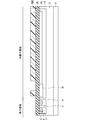
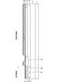
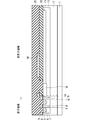
- FIG. 1 is a plan view schematically showing a top surface configuration of the n-type silicon carbide MOSFET 100 according to the first embodiment of the present disclosure.
- the top surface configuration of FIG. 1 is common to all the embodiments.
- n-type silicon carbide MOSFET 100 will be described as a planar gate type, the application of the present disclosure is not limited to the planar gate type, and the application is also applicable to the trench gate type. Further, as long as it has a MOS structure, it is not limited to MOSFETs and can be applied to IGBTs.
- the n-type silicon carbide MOSFET 100 has a quadrangular outer shape, and a gate wiring 103 is provided on the outer edge thereof. Further, in the central portion of the main surface of the n-type silicon carbide MOSFET 100, a cell arrangement region CR in which a plurality of unit cells UC, which are the smallest units of the MOS structure, are arranged is provided.
- the plan view shape of the cell arrangement area CR is such that the central portion of one side forms a quadrangle recessed inward, and the gate pad 102 is provided so as to enter the recessed portion inside the cell arrangement area CR.
- the cell arrangement area CR is separated from the gate pad 102 and the gate wiring 103.
- a gate voltage is applied to the gate pad 102 from an external control circuit (not shown), and the gate voltage applied here is supplied to the gate electrode (not shown) of the unit cell UC through the gate wiring 103. ..
- the cell arrangement area CR is provided with a source pad 101 (source electrode) for connecting the sources of each unit cell in parallel, and the source pad 101 is provided so as to cover almost the entire surface of the cell arrangement area CR.
- FIG. 1 shows the unit cell UC in the source pad 101, which is for convenience.
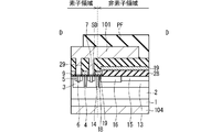
- FIG. 2 is a cross-sectional view taken along the line CC in FIG. 1 and is a cross-sectional view schematically showing the configuration of the unit cell UC.
- the n-type silicon carbide MOSFET 100 is provided on the silicon carbide substrate 1 containing an n-type (first conductive type) impurity in a relatively high concentration.
- a drift layer 2 (semiconductor layer), which is a semiconductor layer containing n-type impurities at a relatively low concentration, is provided on the first main surface of the silicon carbide substrate 1.
- the drift layer 2 is, for example, an epitaxial growth layer formed by epitaxial growth.
- the upper layer of the drift layer 2 is provided with a first well region 3 containing p-type (second conductive type) impurities, and the upper layer of the first well region 3 is provided with a relatively high concentration of p-type impurities.
- the first well contact region 6 included in the above is selectively provided.
- a first source region 5 (first impurity region) containing an n-type impurity at a relatively high concentration is provided so as to be in contact with the two side surfaces of the first well contact region 6.
- the drift layer 2 between the adjacent first well regions 3 is a JFET (Junction Field Effect Transistor) region 4.
- the depth of the drift layer 2 of the first well region 3 from the outermost surface is formed deeper than the depth of the drift layer 2 of the first source region 5 from the outermost surface. Further, the depth of the drift layer 2 of the first well contact region 6 from the outermost surface is equal to or deeper than the depth of the drift layer 2 of the first source region 5 from the outermost surface. The first well area 3 is not exceeded.
- a gate insulating film 8 is formed on the drift layer 2, and a gate electrode 9 is provided on the gate insulating film 8.
- the gate electrode 9 is provided on the edge portion of the JFET region 4, the first well region 3, and the first source region 5.
- An interlayer insulating film 29 is provided on the drift layer 2 including the gate electrode 9, but the first source contact 7 is in contact with a part of the first well contact region 6 and the first source region 5.
- First contact is provided, and for example, a silicide film SD composed of nickel silicide is provided at the bottom of the first source contact 7, and a part of the first well contact region 6 and the first source region 5 is provided. It is covered with a silicide film SD.
- the first well contact region 6 and the first source region 5 are electrically connected to the source pad 101 via the silicide film SD and the first source contact 7.
- a drain electrode 104 is provided on the second main surface opposite to the first main surface of the silicon carbide substrate 1.
- the silicide film SD is not limited to nickel silicide, and aluminum silicide and titanium silicide can also be used.
- the first source contact 7 can be formed by embedding a metal, for example, nickel, aluminum, or titanium, which is a material of the source pad 101, in the contact hole when the source pad 101 is formed.
- the impurity concentration of the drift layer 2 is preferably 1.0 ⁇ 10 14 cm -3 or more and 1.0 ⁇ 10 17 cm -3 or less. It is preferable that the impurity concentration in the JFET region 4 is formed lower than the impurity concentration in the first well region 3. This is so that the depletion layer formed by the pn junction formed in the JFET region 4 and the first well region 3 extends further toward the JFET region 4.
- the impurity concentration in the first well region 3 is preferably 1.0 ⁇ 10 16 cm -3 or more and 1.0 ⁇ 10 20 cm -3 or less.
- the impurity concentration of the first source region 5 is preferably 1.0 ⁇ 10 17 cm -3 or more and 1.0 ⁇ 10 21 cm -3 or less.
- the impurity concentration of the first well contact region 6 is preferably 1.0 ⁇ 10 18 cm -3 or more and 1.0 ⁇ 10 22 cm -3 or less.
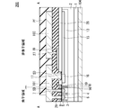
- FIG. 3 is a cross-sectional view taken along the line AA in FIG. 1 and schematically comprises a cell arrangement region CR, that is, an element region in which a semiconductor element is formed and a non-element region in which a semiconductor element is not formed. It is sectional drawing shown in.
- the configuration of the element region is the same as the configuration shown in FIG.
- a second well region 13 containing p-type impurities is provided in the upper layer of the drift layer 2, and the upper layer of the second well region 13 contains n-type impurities in a relatively high concentration.
- a p-type second well contact region 16 that is in contact with the second source region 15 and has a higher impurity concentration than the second well region 13 is selectively provided. ..
- the second source region 15 is formed in a size that occupies most of the upper layer portion of the second well region 13 in the plane direction, and the second well contact region 16 is the remaining portion of the upper layer portion of the second well region 13. Of these, it is provided closer to the element region than the second source region 15 and extends from the pn junction below the second source contact 17 (second contact) to below the boundary gate electrode 19. ing.
- the drift layer 2 between the first well region 3 adjacent to the second well region 13 and the second well region 13 is the outermost JFET region 14.
- the boundary between the element region and the non-element region is defined as the outermost JFET region 14.
- the field insulating film 28 is formed on the second well region 13, penetrates the field insulating film 28, and is electrically connected to the second source region 15 and the second well contact region 16.
- a second source contact 17 is provided.
- a boundary gate electrode 19 is provided on the second well region 13 and the first well region 3 at the boundary between the element region and the non-element region via the boundary gate insulating film 18. The boundary gate electrode 19 extends to the field insulating film 28 above the second source region 15.
- the gate electrode 9 in the element region and the boundary gate electrode 19 are discontinuous, but are continuous in a plan view.
- An interlayer insulating film 29 is provided on the drift layer 2 including the gate electrode 9 and the boundary gate electrode 19, and the gate electrode 9, the boundary gate electrode 19 and the source pad 101 are provided with an interlayer insulating film 29. It is electrically separated.
- the second source contact 17 also penetrates the interlayer insulating film 29 and is electrically connected to the second source region 15 and the second well contact region 16.
- a gate contact 27 is provided so as to penetrate the interlayer insulating film 29 and reach the boundary gate electrode 19 on the field insulating film 28, and the boundary gate electrode 19 and the gate electrode 9 pass through the gate contact 27. It is electrically connected to the gate wiring 103.
- a protective film PF is provided on the gate wiring 103 and the source pad 101 in the non-element region, and on a part of the source pad 101 in the element region.
- the protective film PF is composed of an insulating film.
- a silicide film SD composed of nickel silicide is provided at the bottom of the second source contact 17, and a part of the second source region 15 and the second well contact region 16 is covered with the silicide film SD.
- the second well contact region 16 and the second source region 15 are electrically connected to the source pad 101 via the silicide film SD and the second source contact 17.
- the silicide film SD is not limited to nickel silicide, and aluminum silicide and titanium silicide can also be used.
- the first source contact 7 can be formed by embedding a metal, for example, nickel, aluminum, or titanium, which is a material of the source pad 101, in the contact hole when the source pad 101 is formed.
- the impurity concentration of the second well region 13 is preferably 1.0 ⁇ 10 16 cm -3 or more and 1.0 ⁇ 10 20 cm -3 or less.
- the impurity concentration of the second source region 15 is preferably 1.0 ⁇ 10 17 cm -3 or more and 1.0 ⁇ 10 21 cm -3 or less.
- the impurity concentration of the second well contact region 16 is preferably 1.0 ⁇ 10 18 cm -3 or more and 1.0 ⁇ 10 22 cm -3 or less.
- the length of the second well contact region 16 extending from the lower pn junction of the second source contact 17 to the element region side is 1.0 ⁇ m or more and 100 ⁇ m or less. By setting it in such a range, it is possible to take a margin in the dimensional design of the silicon carbide semiconductor device.
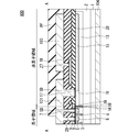
- FIG. 4 is a cross-sectional view taken along the line BB in FIG. 1 and is a cross-sectional view schematically showing the configuration of an element region and a formation region of a gate pad 102 which is a non-element region. As shown in FIG. 4, the configurations of the element region and the non-element region are the same as those shown in FIG.
- FIG. 5 is a plan view schematically showing the configurations of the element region and the non-element region in the region X in FIG. 1.
- the insulating film and electrodes on the drift layer 2 are omitted, and only the configuration of the upper layer portion of the drift layer 2 is shown.
- the plan view shape of the unit cell UC in the element region is square and arranged in a matrix, but this is an example and is not limited to this shape, but is a rectangle. It can also be a polygon.
- the first source region 5 surrounds the first well contact region 6 having a square outer shape, and the outside thereof is surrounded by the first well region 3.
- the unit cell UCs are in the JFET region 4, and the corners between the unit cells UCs adjacent to each other in the diagonal direction are connected by the first well region 3.
- the second well contact region 16 is provided so as to be continuous with the second well contact region 13 and the second source region 15 is provided so as to be continuous with the second well contact region 16.
- the second well contact region 16 is continuously formed so as to extend below the plurality of second source contacts 17 in a plan view, and similarly, the second source region 15 is a plurality of second source contacts 17 in a plan view. It is continuously provided so as to extend below.
- FIG. 6 is a cross-sectional view taken along the line DD in FIG. 5 and is a cross-sectional view schematically showing the configuration of an element region and a non-element region.
- a plurality of second source contacts 17 are provided apart from each other, and between the plurality of second source contacts 17, as shown in FIG. 6, the boundary gate electrode 19 is an element region.
- the gate signal applied to the gate wiring 103 can be transmitted to the gate electrode 9 in the element region via the gate contact 27.
- FIGS. 7 to 18 are cross-sectional views showing the manufacturing process in order.
- the plane orientation of the first main surface is the (0001) plane, and the surface orientation is on the first main surface of the n-type low-resistance silicon carbide substrate 1 having a polytype of 4H.
- the n-type drift layer 2 of silicon carbide is epitaxially grown by a chemical vapor deposition (CVD) method.
- the concentration of n-type impurities in the drift layer 2 is, for example, 1 ⁇ 10 14 cm -3 to 1 ⁇ 10 17 cm -3, and the thickness of the drift layer 2 is, for example, 5 ⁇ m to 50 ⁇ m.
- an injection mask (not shown) is formed on the drift layer 2 by a photoresist or the like, and Al (aluminum), which is a p-type impurity, is ion-implanted into the upper layer of the drift layer 2 to form a p-type.
- the 1-well region 3 and the 2nd well region 13 are formed.
- the depth of ion implantation of Al is set to a depth that does not exceed the thickness of the drift layer 2, for example, 0.5 to 3 ⁇ m.
- the impurity concentration of the ion-implanted Al is, for example, 1 ⁇ 10 16 cm -3 to 1 ⁇ 10 20 cm -3 , which is higher than the n-type impurity concentration of the drift layer 2.
- the implantation mask is removed.
- the first well region 3 and the second well region 13 are formed in the same step, but they can also be formed in different steps.
- an injection mask (not shown) is formed on the drift layer 2 by a photoresist or the like, N (nitrogen), which is an n-type impurity, is ion-implanted, and the first well region 3 is formed.
- N nitrogen
- the n-type first source region 5 is formed in the upper layer portion
- the second source region 15 is formed in the upper layer portion of the second well region 13.
- the ion implantation depth of N is shallower than the thickness of the first well region 3 and the second well region 13.
- the impurity concentration of the ion-implanted N is, for example, 1 ⁇ 10 17 cm -3 to 1 ⁇ 10 21 cm -3 , which is higher than the p-type impurity concentration in the first well region 3 and the second well region 13, respectively. do.
- the implantation mask is removed.
- the first source region 5 and the second source region 15 are formed in the same step, but they can also be formed in separate steps.
- an injection mask (not shown) is formed on the drift layer 2 by a photoresist or the like, Al, which is a p-type impurity, is ion-implanted, and the upper layer portion of the first well region 3 is formed.
- the p-type first well contact region 6 is formed in the above, and the second well contact region 16 is formed in the upper layer of the second well region 13.
- the first well contact region 6 is formed at a depth that is electrically connected to the first well region 3 from the outermost surface of the first source region 5.
- the second well contact region 16 is formed at a depth that is electrically connected to the second well region 13 from the outermost surface of the second source region 15.
- the first well contact region 6 is provided in order to obtain good electrical contact between the first well region 3 and the first source contact 7 that electrically connects the source pad 101.
- the p-type impurity concentration in the first well contact region 6 and the second well contact region 16 is higher than the p-type impurity concentration in the first well region 3 and the second well contact region 13, respectively.
- the implantation mask is removed.
- the first well contact region 6 and the second well contact region 16 are formed in the same step, but they can also be formed in separate steps.
- an injection mask RM1 is formed on the drift layer 2 by a photoresist or the like, N, which is an n-type impurity, is ion-injected into the JFET region 4 and the outermost JFET region 14.
- N which is an n-type impurity
- the concentration of n-type impurities in the JFET region 4 and the outermost JFET region 14 is made higher than the concentration of n-type impurities in the drift layer 2.
- the impurity concentration of the ion-implanted N is lower than the p-type impurity concentration in the first well region 3.
- the impurities concentration in the JFET region 4 and the outermost JFET region 14 is relatively lower than that in the first well region 3, so that the first well region 3 and the JFET region 4 and the outermost JFET region 14 are separated from each other. This is to allow the depletion layer to extend to the JFET region 4 and the outermost JFET region 14 side when a reverse bias is applied to the pn junction formed between them.
- the injection mask RM1 is removed.
- the JFET region 4 and the outermost JFET region 14 having a higher impurity concentration than the drift layer 2 are formed by injecting n-type impurities, but the injection of n-type impurities is not always necessary. It is also possible to inject p-type impurities. Further, the impurity concentration in the JFET region 4 and the outermost JFET region 14 can be the same as the impurity concentration in the drift layer 2.
- an n-type or p-type epitaxial layer EP is epitaxially grown on the drift layer 2.
- the thickness of the epitaxial layer EP can be 10 to 500 nm.
- the epitaxial layer EP is provided as an epitaxial channel layer in which a channel is formed, but it is not an essential configuration and is not shown in FIGS. 2 to 4 and the figures shown below.
- the field insulating film 28 is formed on the drift layer 2 by the reduced pressure CVD method, and the etching mask RM2 is formed on the field insulating film 28 by a photoresist or the like. Then, the field insulating film 28 is partially etched and removed. The portion to be removed is a portion where the gate insulating film 8 and the boundary gate insulating film 18 are formed later. After that, the etching mask RM2 is removed.
- the surface of the drift layer 2 is thermally oxidized to form the gate insulating film 8 having a desired thickness.
- a polycrystalline silicon (polysilicon) film having conductivity is formed on the gate insulating film 8 by a reduced pressure CVD method, and the gate electrode 9 and the gate electrode 9 and the gate electrode 9 are patterned by etching.
- the boundary gate electrode 19 is formed. Further, the gate insulating film 8 not covered by the gate electrode 9 and the boundary gate electrode 19 is removed by etching or the like. Here, the gate insulating film 8 located below the boundary gate electrode 19 becomes the boundary gate insulating film 18.
- an interlayer insulating film 29 is formed on the drift layer 2 including the gate electrode 9 and the boundary gate electrode 19 by the reduced pressure CVD method.
- the second source contact hole 17C that penetrates the gate insulating film 8 and reaches the second well contact region 16 and the second source region 15 is formed.
- a gate contact hole 27C that penetrates the interlayer insulating film 29 and reaches the gate electrode 9 is formed.
- a metal film MF containing, for example, nickel (Ni) as a main component is formed on the interlayer insulating film 29 by a sputtering method or the like, and heat treatment is performed at a temperature of 600 ° C. or higher and 1100 ° C. or lower.
- a metal film MF containing Ni as a main component and silicon carbide are reacted to form a silicide film SD.
- the metal film MF remaining on the interlayer insulating film 29 other than the silicide film SD is removed by wet etching. Ohmic contact is formed on the bottom surfaces of the first source contact hole 7C and the second source contact hole 17C by the silicide film SD.
- a metal film containing Ni as a main component is formed on the second main surface (back surface) of the silicon carbide substrate 1, and the back surface is contacted with the back surface of the silicon carbide substrate 1 by heat treatment.
- a metal layer such as Al is formed on the front surface of the silicon carbide substrate 1 on which the interlayer insulating film 29 is formed by a sputtering method or a thin-film deposition method, and processed into a predetermined shape by a photolithography technique to form a first source contact. 7.
- the second source contact 17 and the gate contact 27 are formed, and the source pad 101 connected to the first source contact 7 and the second source contact 17 and the gate wiring 103 connected to the gate contact 27 are formed.
- the gate pad 102 (FIG. 4) connected to the gate wiring 103 is also formed. Further, a metal layer such as Al is formed on the back surface contact of the back surface of the silicon carbide substrate 1 by a sputtering method or a thin film deposition method to form a drain electrode 104. After that, by forming a protective film PF (FIG. 3) on the gate wiring 103 and the source pad 101 in the non-element region and a part of the upper part of the source pad 101 in the element region with an insulating film or the like, the n-type is formed. The silicon carbide MOSFET 100 is completed.
- the second well contact region 16 extends from the pn junction below the second source contact 17 to the element region side and extends to the element region side.
- Reference numeral 15 is provided so as to extend from the pn junction below the second source contact 17 toward the non-element region side.
- the second well contact region 16 is continuously formed so as to extend below the plurality of second source contacts 17 in a plan view, and similarly, the second source region 15 is formed. It is continuously provided so as to extend below the plurality of second source contacts 17 in a plan view. Therefore, when the n-type silicon carbide MOSFET 100 switches from the off state to the on state, the displacement current flowing in from the second source contact 17 can be dispersed, and the concentration of the displacement current can be avoided.
- the second source contact 17 is made of a metal such as nickel, aluminum, or titanium, and the bottom of the second source contact 17 is formed with a silicide film SD of silicon carbide and a metal to form a second source region 15 and a metal. Good ohmic contact is formed in both of the second well contact areas 16.
- the second source contact 17 and the second source contact 17 are formed.
- the contact resistance value (contact differential resistance value) per unit area with the 2-well contact region 16 is larger than the contact differential resistance value between the second source contact 17 and the second source region 15.
- the area of the second well contact region 16 below the second source contact 17 is made as large as possible. It is preferable to do so. Specifically, it is preferable that the area of the second well contact region 16 below the second source contact 17 is 1 to 100 times the area of the second source region 15 below the second source contact 17. Is.
- the impurity concentration in the second source region 15 is 1.0 ⁇ 10 17 cm -3 or more and 1.0 ⁇ 10 21 cm -3 or less, more preferably 1 ⁇ 10 19 cm -3 or more and 1 ⁇ 10 20 cm ⁇ . 3 or less.
- the impurity concentration in the second well contact region 16 is 1.0 ⁇ 10 18 cm -3 or more and 1.0 ⁇ 10 22 cm -3 or less, more preferably 1.0 ⁇ 10 19 cm -3 or more and 1.0. ⁇ 10 21 cm -3 or less.
- the sheet resistance value of the second source region 15 is lower than the sheet resistance value of the second well contact region 16. This facilitates the flow of current in the second source region 15.
- the n-type silicon carbide MOSFET 100 switches from the off state to the on state, for example, between a large dV / dt (time fluctuation of voltage) source of 20 V / n sec or more and a drain.
- a larger proportion of the displacement current flowing in from the second source contact 17 can flow through the second source region to the non-element region side of the second source contact 17 and to the second. It is possible to suppress the displacement current flowing toward the element region side of the source contact 17. Therefore, the voltage generated at the end of the second well region 13 on the element region side (the end of the second well region 13) can be reduced, and the voltage between the end of the second well region 13 and the boundary gate electrode 19 can be reduced. The potential difference is suppressed, the dielectric breakdown of the boundary gate insulating film 18 is suppressed, and the reliability as a semiconductor device is improved.
- FIG. 19 is a cross-sectional view showing the configuration of the n-type silicon carbide MOSFET 200 according to the second embodiment, and corresponds to the cross-sectional view taken along the line AA in FIG.
- the portion extending from the pn junction below the second source contact 17 of the second well contact region 16 toward the element region is directly below the field insulating film 28. It extends only to, and does not reach directly below the boundary gate electrode 19.
- FIG. 20 is a cross-sectional view taken along the line BB in FIG. 1 and is a cross-sectional view schematically showing the configuration of an element region and a formation region of a gate pad 102 which is a non-element region. As shown in FIG. 20, the configuration of the element region and the non-element region is the same as the configuration shown in FIG.
- the boundary portion is on the second well contact region 16 having a high concentration.
- the gate insulating film 18 is not formed, and the film quality of the boundary gate insulating film 18 is improved. That is, since the crystal structure is broken in the high-concentration impurity injection region, the homogeneity of the boundary gate insulating film 18 formed on the crystal structure is deteriorated, but this occurs in the configuration of the n-type silicon carbide MOSFET 200. However, the film quality evaluated by withstand voltage and leakage current is improved. Therefore, the effect of suppressing the dielectric breakdown of the boundary gate insulating film 18 becomes higher, and the reliability as a semiconductor device is further improved.
- FIG. 21 is a plan view showing the configuration of the element region and the non-element region of the n-type silicon carbide MOSFET 300 of the third embodiment, and corresponds to the plan view of the region X in FIG.
- the insulating film and electrodes on the drift layer 2 are omitted, and only the configuration of the upper layer portion of the drift layer 2 is shown.
- the same components as those described with reference to FIG. 5 are designated by the same reference numerals, and duplicate description will be omitted.
- the length of the portion extending from the junction with the second source region 15 to the element region side is the second. 2 It is shorter than the length of the portion extending from the lower pn junction of the source contact 17 to the element region side. Then, the length of the second source region 15 is formed longer by the amount that the length of the second well contact region 16 is shortened.
- the second well contact region 16 is partially recessed toward the element region, and the second source region 15 is partially projected.
- the second well contact region 16 is recessed and the second source region 15 is projected at only one portion between the two second source contacts 17, but typically. Since a plurality of second source contacts 17 are provided along the gate wiring 103 in the non-elemental region, the second well contact region 16 is recessed between the second source contacts 17, and the portion where the second source region 15 protrudes is formed. Can be provided.
- FIG. 22 is a cross-sectional view taken along the line DD in FIG. 21 in the direction indicated by the arrow.
- the length of the second well contact region 16 is the element region from the junction with the second source region 15 of the n-type silicon carbide MOSFET 100 shown in FIG.
- the second well contact region 16 extending to the side is formed shorter than the length, and the second source region 15 is formed longer by that amount.
- the second source is used when the n-type silicon carbide MOSFET 300 switches from the off state to the on state.
- a larger percentage of the displacement current flowing in from the contact 17 can flow through the lengthened second source region 15 towards the non-device region more than the second source contact 17 and more than the second source contact 17.
- the displacement current flowing on the element region side can be further suppressed. Therefore, the voltage generated at the end of the second well region 13 on the element region side (the end of the second well region 13) can be further reduced, and between the end of the second well region 13 and the boundary gate electrode 19.
- the potential difference between the two is further suppressed, the effect of suppressing the dielectric breakdown of the boundary gate insulating film 18 is further enhanced, and the reliability as a semiconductor device is further improved.
- FIG. 23 is a cross-sectional view showing the configuration of the n-type silicon carbide MOSFET 400 according to the fourth embodiment, and corresponds to the cross-sectional view taken along the line AA in FIG.
- the portion extending from the pn junction below the second source contact 17 of the second well contact region 16 toward the element region is the portion of the second well contact region 13. It is provided up to the end (the 13th end of the second well region).
- FIG. 24 is a cross-sectional view taken along the line BB in FIG. 1 and is a cross-sectional view schematically showing the configuration of an element region and a formation region of a gate pad 102 which is a non-element region. As shown in FIG. 24, the configuration of the element region and the non-element region is the same as the configuration shown in FIG. 23.
- the n-type silicon carbide MOSFET 400 of the fourth embodiment since the second well contact region 16 is provided up to the end of the second well region 13, the n-type silicon carbide MOSFET 400 switches from the off state to the on state. At the same time, the voltage generated at the end of the second well region 13 can be effectively reduced.
- the sheet resistance value of the second well contact region 16 is lower than the sheet resistance of the second well contact region 13
- the voltage generated at the end of the second well contact region 16 is generated at the end of the second well region 13. It can be lower than the voltage to be applied.
- the potential difference between the end of the second well region 13 and the boundary gate electrode 19 is further suppressed, the effect of suppressing dielectric breakdown of the boundary gate insulating film 18 is further increased, and the reliability as a semiconductor device is further increased. improves.
- each embodiment can be freely combined, and each embodiment can be appropriately modified or omitted within the scope of the disclosure.
Landscapes
- Engineering & Computer Science (AREA)
- Microelectronics & Electronic Packaging (AREA)
- Power Engineering (AREA)
- Physics & Mathematics (AREA)
- Ceramic Engineering (AREA)
- Condensed Matter Physics & Semiconductors (AREA)
- General Physics & Mathematics (AREA)
- Computer Hardware Design (AREA)
- Chemical & Material Sciences (AREA)
- Crystallography & Structural Chemistry (AREA)
- Manufacturing & Machinery (AREA)
- Electrodes Of Semiconductors (AREA)
Abstract
本開示は炭化珪素半導体装置に関し、半導体層の上層部に設けられたp型の第2ウェル領域と、その上層部に設けられたn型の第2不純物領域と、第2ウェル領域の上層部に設けられ、側面において第2不純物領域に接合するp型の第2ウェルコンタクト領域と、第2ウェル領域上に設けられたフィールド絶縁膜と、フィールド絶縁膜を貫通して、第2不純物領域および第2ウェルコンタクト領域にオーミック接触し、第1主電極に電気的に接続される第2コンタクトと、素子領域と非素子領域との境界の側の第2不純物領域の端縁部上から、境界に隣り合う第1ウェル領域内の第1不純物領域の端縁部上にかけて設けられた境界部ゲート絶縁膜と、その上の境界部ゲート電極と、第2主電極と、を備え、第2ウェルコンタクト領域は、第2コンタクトの下方から素子領域側に延在し、第2不純物領域は、第2コンタクトの下方から非素子領域側に延在する。
Description
本開示は炭化珪素半導体装置に関し、特に、ゲート絶縁膜を有する炭化珪素半導体装置に関する。
インバータ回路などに用いられるスイッチング素子として、縦型の電力用半導体装置が広く用いられており、特に、MOS(Metal Oxide Semiconductor)構造を有する電力用半導体装置が広く用いられている。典型的には、絶縁ゲートバイポーラトランジスタ(Insulated Gate Bipolar Transistor:IGBT)、および、MOSFET(Metal Oxide Semiconductor Field Effect Transistor)が用いられている。
シリコン(Si)のバンドギャップに比して約3倍大きなバンドギャップを有する炭化珪素を半導体材料として用いる炭化珪素半導体装置の1つであるn型MOSFETは、インバータ回路のスイッチング素子として用いることでインバータ回路の電力損失を低減することができる。
n型MOSFETは、典型的には、n型ドリフト層と、その上に設けられたp型ウェルとを有しており、MOSFETがオン状態からオフ状態へとスイッチングされると、MOSFETのドレイン電圧、すなわちドレイン電極の電圧が急激に上昇して、略0Vから数百Vへ変化する。そうすると、p型ウェルとn型ドリフト層との間に存在する寄生容量を介して変位電流が発生する。ドレイン電極側に発生した変位電流はドレイン電極へと流れ、ソース電極側に発生した変位電流はp型ウェルを経由してソース電極へと流れる。また、MOSFETがオフ状態からオン状態へとスイッチングされると、オン状態からオフ状態へとスイッチングされる場合とは逆方向の変位電流がp型ウェルを経由して流れる。
特許文献1には、ゲートパッドの下方に位置する最外周のp型ウェル上に、ゲート絶縁膜よりも膜厚が厚いフィールド絶縁膜を貫通して、ソース電極に接続するウェルコンタクトホールが設けられている。これにより、ゲートパッドの下方に位置する大面積のp型ウェル内を流れる変位電流の大部分が、ウェルコンタクトホールを経由してソース電極に流れ、大面積のp型ウェルとはウェルコンタクトホールの反対側に形成されるゲート絶縁膜直下のp型ウェルとゲート電極との間に高電界が発生することを抑制して、ゲート絶縁膜の絶縁破壊を防止する構成が開示されている。
特許文献1に開示の技術によれば、ウェルコンタクトホールの最外周p型ウェル端側では、フィールド絶縁膜からゲート絶縁膜に厚さが変わる部分で段差がウェルコンタクトホールと最外周のp型ウェル端側との間に設けられることになるので、ウェルコンタクトホールと最外周のp型ウェル端側との間に距離を設ける必要が生じる。そのため、最外周のp型ウェル端側からウェルコンタクトホールに流れる変位電流によって最外周のp型ウェルに発生する電位とゲート電極の電位との間に生じる電界がゲート絶縁膜に印加される。
最外周のp型ウェルに生じる変位電流の大部分は、ウェルコンタクトホールの最外周のp型ウェル端側と反対側の大面積の最外周のp型ウェルに流れるため、通常は最外周のp型ウェル端には高電圧は発生せず、ゲート絶縁膜に高電界は生じない。
しかしながら、昨今では、時間tに対するドレイン電圧Vの変動であるdV/dtをより一層大きくすることが求められており、例えば、20V/nsec以上の大きなdV/dtが要求される場合には、ウェルコンタクトホールと最外周のp型ウェル端側との間の距離が無視できなくなり、最外周のp型ウェル端側からウェルコンタクトホールに無視できない大きさの変位電流が流れ、最外周のp型ウェル端に高電圧が発生し、ゲート絶縁膜が絶縁破壊する可能性があった。
本開示は、上記のような問題を解決するためになされたものであり、大きなdV/dtが印加された場合でも、ゲート絶縁膜に生じる電界を抑制できる炭化珪素半導体装置を提供することを目的とする。
本開示に係る炭化珪素半導体装置は、半導体素子が形成された素子領域と、該素子領域以外の非素子領域とを有し、前記素子領域において、炭化珪素基板の厚み方向に主電流が流れ、前記炭化珪素基板の第1の主面上に設けられた第1導電型の半導体層と、前記素子領域の前記半導体層の上層部に設けられた第2導電型の第1ウェル領域と、前記第1ウェル領域の上層部に設けられた第1導電型の第1不純物領域と、前記第1ウェル領域の上層部に設けられ、側面において前記第1不純物領域に接合する第2導電型の第1ウェルコンタクト領域と、第1不純物領域の端縁部上、前記第1ウェル領域上および前記半導体層上に設けられたゲート絶縁膜と、前記ゲート絶縁膜上に設けられたゲート電極と、前記第1不純物領域および前記第1ウェルコンタクト領域にオーミック接触し、前記半導体層の上方に設けられた第1主電極に電気的に接続される第1コンタクトと、前記非素子領域の前記半導体層の上層部に設けられた第2導電型の第2ウェル領域と、前記第2ウェル領域の上層部に設けられた第1導電型の第2不純物領域と、前記第2ウェル領域の上層部に設けられ、側面において前記第2不純物領域に接合する第2導電型の第2ウェルコンタクト領域と、前記第2ウェル領域上に設けられたフィールド絶縁膜と、前記フィールド絶縁膜を貫通して、前記第2不純物領域および前記第2ウェルコンタクト領域にオーミック接触し、前記第1主電極に電気的に接続される少なくとも1つの第2コンタクトと、前記素子領域と前記非素子領域との境界の側の前記第2不純物領域の端縁部上から、前記境界に隣り合う前記第1ウェル領域内の前記第1不純物領域の端縁部上にかけて設けられた境界部ゲート絶縁膜と、前記境界部ゲート絶縁膜上に設けられた境界部ゲート電極と、前記炭化珪素基板の前記第1の主面とは反対側の第2の主面上に設けられた第2主電極と、を備え、前記第2ウェルコンタクト領域は、前記少なくとも1つの第2コンタクトの下方から前記素子領域側に延在し、前記第2不純物領域は、前記少なくとも1つの第2コンタクトの下方から前記非素子領域側に延在する。
本開示に係る炭化珪素半導体装置によれば、オフ状態からオン状態にスイッチングする場合に、第2不純物領域が形成されていることにより、少なくとも1つの第2コンタクトから流入する変位電流のより多くを、少なくとも1つの第2コンタクトよりも非素子領域側に流すことができる。そのため、第2コンタクトよりも素子領域側に流れる変位電流を低減することができ、第2ウェル領域の端部と境界部ゲート電極との間の電位差が抑制され、境界部ゲート絶縁膜の絶縁破壊を抑制できる。
<はじめに>
以下の説明において、「素子領域」とは半導体素子のオン状態において主電流が流れる領域である。また、以下において、「外側」とは半導体素子の外周に向かう方向であり、「内側」とは「外側」に対して反対の方向とする。
以下の説明において、「素子領域」とは半導体素子のオン状態において主電流が流れる領域である。また、以下において、「外側」とは半導体素子の外周に向かう方向であり、「内側」とは「外側」に対して反対の方向とする。
なお、図面は模式的に示されるものであり、異なる図面にそれぞれ示されている画像のサイズおよび位置の相互関係は、必ずしも正確に記載されるものではなく、適宜変更され得る。また、以下の説明では、同様の構成要素には同じ符号を付して図示し、それらの名称および機能も同様のものとする。よって、それらについての詳細な説明を省略する場合がある。また、本明細書において、「~上」および「~を覆う」という場合、構成要素間に介在物が存在することが妨げられるものではない。例えば、「A上に設けられたB」または「AがBを覆う」と記載している場合、AとBとの間に他の構成要素Cが設けられたものも設けられていないものも意味され得る。また、以下の説明では、「上」、「下」、「側」、「底」、「表」または「裏」などの特定の位置および方向を意味する用語が用いられる場合があるが、これらの用語は、実施の形態の内容を理解することを容易にするため便宜上用いられているものであり、実際に実施される際の方向とは関係しない。
また、「MOS」という用語は、古くは金属-酸化物-半導体の接合構造に用いられているが、特にMOS構造を有するMOS電界効果トランジスタ(MOSFET)においては、近年の集積化や製造プロセスの改善などの観点からゲート絶縁膜およびゲート電極の材料が改善されている。
例えばMOSFETにおいては、主としてソース・ドレインを自己整合的に形成する観点から、ゲート電極の材料として金属の代わりに多結晶珪素が採用されてきている。また電気的特性を改善する観点から、ゲート絶縁膜の材料として高誘電率の材料が採用されるが、当該材料は必ずしも酸化物には限定されない。
従って「MOS」という用語は必ずしも金属-酸化物-半導体の積層構造のみに限定されて採用されているわけではなく、本明細書でもそのような限定を前提としない。すなわち、技術常識に鑑みて、ここでは「MOS」とはその語源に起因した略語としてのみならず、広く導電体-絶縁体-半導体の積層構造をも含む意義を有する。
以下、図面に基づいて実施の形態について説明する。なお、以下の図面において同一または相当する部分には同一の参照符号を付しその説明は繰返さない。
また、以下に説明する実施の形態1~4においては、炭化珪素半導体装置の一例として、主電流が基板の厚み方向に流れる縦型のn型MOSFETを用いて説明する。
<実施の形態1>
<装置構成>
図1は、本開示に係る実施の形態1のn型炭化珪素MOSFET100の上面構成を模式的に示す平面図である。なお、全ての実施の形態においては図1の上面構成は共通である。
<装置構成>
図1は、本開示に係る実施の形態1のn型炭化珪素MOSFET100の上面構成を模式的に示す平面図である。なお、全ての実施の形態においては図1の上面構成は共通である。
また、n型炭化珪素MOSFET100はプレーナゲート型として説明するが、本開示の適用はプレーナゲート型に限定されず、トレンチゲート型にも適用可能である。また、MOS構造を有するのであればMOSFETに限定されず、IGBTにも適用可能である。
図1に示されるように、n型炭化珪素MOSFET100は四角形状の外形を有し、その外縁にはゲート配線103が設けられている。また、n型炭化珪素MOSFET100の主面の中央部には、MOS構造の最小単位であるユニットセルUCが複数配置されたセル配置領域CRが設けられている。
セル配置領域CRの平面視形状は、一辺の中央部が内側に凹んだ四角形をなし、セル配置領域CRの内側に凹んだ部分に入り込むようにゲートパッド102が設けられている。なお、セル配置領域CRとゲートパッド102およびゲート配線103とは離間している。
ゲートパッド102には、外部の制御回路(図示せず)からゲート電圧が印加され、ここに印加されたゲート電圧は、ゲート配線103を通じてユニットセルUCのゲート電極(図示せず)に供給される。
また、セル配置領域CRには、各ユニットセルのソースを並列に接続するソースパッド101(ソース電極)が設けられており、ソースパッド101はセル配置領域CRのほぼ全面を覆うように設けられている。なお、図1ではユニットセルUCをソースパッド101中に図示しているがこれは便宜的なものである。
図2は、図1におけるC-C線での矢示方向断面図であり、ユニットセルUCの構成を模式的に示す断面図である。図2に示されるように、n型炭化珪素MOSFET100は、n型(第1導電型)不純物を比較的高濃度に含む炭化珪素基板1上に設けられている。
炭化珪素基板1の第1の主面上には、n型不純物を比較的低濃度に含む半導体層であるドリフト層2(半導体層)が設けられている。ドリフト層2は、例えばエピタキシャル成長により形成されたエピタキシャル成長層である。
ドリフト層2の上層部には、p型(第2導電型)不純物を含む第1ウェル領域3が設けられており、第1ウェル領域3の上層部には、p型不純物を比較的高濃度に含む第1ウェルコンタクト領域6が選択的に設けられている。そして、第1ウェルコンタクト領域6の2つの側面に接するようにn型不純物を比較的高濃度に含む第1ソース領域5(第1不純物領域)が設けられている。なお、隣り合う第1ウェル領域3の間のドリフト層2はJFET(Junction Field Effect Transistor)領域4となっている。
なお、第1ウェル領域3のドリフト層2の最表面からの深さは、第1ソース領域5のドリフト層2の最表面からの深さよりも深く形成されている。また、第1ウェルコンタクト領域6のドリフト層2の最表面からの深さは、第1ソース領域5のドリフト層2の最表面からの深さと同等か、それよりも深く形成されているが、第1ウェル領域3は超えない。
ドリフト層2の上には、ゲート絶縁膜8が形成され、ゲート絶縁膜8上にはゲート電極9が設けられている。ゲート電極9は、JFET領域4、第1ウェル領域3および第1ソース領域5の端縁部上に設けられる。
そして、ゲート電極9上を含むドリフト層2上には層間絶縁膜29が設けられているが、第1ウェルコンタクト領域6と第1ソース領域5の一部に接触するように第1ソースコンタクト7(第1コンタクト)が設けられ、第1ソースコンタクト7の底部には、例えば、ニッケルシリサイドで構成されるシリサイド膜SDが設けられ、第1ウェルコンタクト領域6および第1ソース領域5の一部はシリサイド膜SDで覆われている。第1ウェルコンタクト領域6と第1ソース領域5はシリサイド膜SDおよび第1ソースコンタクト7を介して、ソースパッド101に電気的に接続されている。また、炭化珪素基板1の第1の主面とは反対側の第2の主面上には、ドレイン電極104が設けられている。
シリサイド膜SDはニッケルシリサイドに限定されず、アルミシリサイド、チタンシリサイドを用いることもできる。第1ソースコンタクト7は、ソースパッド101形成時に、コンタクトホール内にソースパッド101の材料となる金属、例えば、ニッケル、アルミニウム、チタンを埋め込むことで形成することができる。
ドリフト層2の不純物濃度は、1.0×1014cm-3以上1.0×1017cm-3以下であることが好適である。JFET領域4の不純物濃度は、第1ウェル領域3の不純物濃度よりも低く形成することが好適である。これは、JFET領域4と第1ウェル領域3とで形成されるpn接合による空乏層が、よりJFET領域4側に延伸するようにするためである。第1ウェル領域3の不純物濃度は、1.0×1016cm-3以上1.0×1020cm-3以下であることが好適である。第1ソース領域5の不純物濃度は、1.0×1017cm-3以上1.0×1021cm-3以下であることが好適である。第1ウェルコンタクト領域6の不純物濃度は、1.0×1018cm-3以上1.0×1022cm-3以下であることが好適である。
図3は、図1におけるA-A線での矢示方向断面図であり、セル配置領域CR、すなわち半導体素子が形成された素子領域と、半導体素子が形成されない非素子領域の構成を模式的に示す断面図である。
図3に示されるように、素子領域の構成は図2に示した構成と同様である。非素子領域においては、ドリフト層2の上層部にp型不純物を含む第2ウェル領域13が設けられており、第2ウェル領域13の上層部には、n型不純物を比較的高濃度に含む第2ソース領域15(第2不純物領域)と、第2ソース領域15に接し、第2ウェル領域13よりも高い不純物濃度を有するp型の第2ウェルコンタクト領域16が選択的に設けられている。第2ソース領域15は、平面方向において第2ウェル領域13の上層部の大部分を占める大きさに形成され、第2ウェルコンタクト領域16は、第2ウェル領域13の上層部の残りの部分のうち、第2ソース領域15よりも素子領域に近い側に設けられ、第2ソースコンタクト17(第2コンタクト)の下方のpn接合部から境界部ゲート電極19の下方まで延在するように設けられている。
素子領域の複数の第1ウェル領域3のうち、第2ウェル領域13と隣り合う第1ウェル領域3と、第2ウェル領域13との間のドリフト層2は最外周JFET領域14となっており、素子領域と非素子領域との境界は最外周JFET領域14と定義する。
非素子領域においては、第2ウェル領域13上にフィールド絶縁膜28が形成され、フィールド絶縁膜28を貫通して、第2ソース領域15と第2ウェルコンタクト領域16とに電気的に接続される第2ソースコンタクト17が設けられている。また、素子領域と非素子領域との境界の第2ウェル領域13上および第1ウェル領域3上には境界部ゲート絶縁膜18を介して境界部ゲート電極19が設けられている。なお、境界部ゲート電極19は、第2ソース領域15の上方のフィールド絶縁膜28上にまで延在している。図3では、素子領域のゲート電極9と境界部ゲート電極19とは不連続であるが、平面視では連続している。
ゲート電極9上および境界部ゲート電極19上を含むドリフト層2上には層間絶縁膜29が設けられており、ゲート電極9および境界部ゲート電極19とソースパッド101とは、層間絶縁膜29により電気的に離間されている。第2ソースコンタクト17は層間絶縁膜29も貫通して、第2ソース領域15と第2ウェルコンタクト領域16と電気的に接続されている。また、層間絶縁膜29を貫通してフィールド絶縁膜28上の境界部ゲート電極19に達するようにゲートコンタクト27が設けられており、境界部ゲート電極19およびゲート電極9はゲートコンタクト27を介してゲート配線103に電気的に接続される。
非素子領域のゲート配線103上およびソースパッド101上と、素子領域のソースパッド101の一部上部には保護膜PFが設けられている。保護膜PFは絶縁膜で構成されている。
第2ソースコンタクト17の底部には、例えば、ニッケルシリサイドで構成されるシリサイド膜SDが設けられ、第2ソース領域15および第2ウェルコンタクト領域16の一部はシリサイド膜SDで覆われている。第2ウェルコンタクト領域16と第2ソース領域15はシリサイド膜SDおよび第2ソースコンタクト17を介して、ソースパッド101に電気的に接続されている。なお、シリサイド膜SDはニッケルシリサイドに限定されず、アルミシリサイド、チタンシリサイドを用いることもできる。第1ソースコンタクト7は、ソースパッド101形成時に、コンタクトホール内にソースパッド101の材料となる金属、例えば、ニッケル、アルミニウム、チタンを埋め込むことで形成することができる。
第2ウェル領域13の不純物濃度は、1.0×1016cm-3以上1.0×1020cm-3以下であることが好適である。第2ソース領域15の不純物濃度は、1.0×1017cm-3以上1.0×1021cm-3以下であることが好適である。第2ウェルコンタクト領域16の不純物濃度は、1.0×1018cm-3以上1.0×1022cm-3以下であることが好適である。このような濃度範囲とすることで、所望の定格を有する炭化珪素半導体装置を得ることができる。
また、第2ウェルコンタクト領域16が、第2ソースコンタクト17の下方のpn接合部から素子領域側に延在する長さは、1.0μm以上100μm以下であることが好適である。このような範囲に設定することで炭化珪素半導体装置の寸法設計上のマージンを取ることができる。
図4は、図1におけるB-B線での矢示方向断面図であり、素子領域と、非素子領域であるゲートパッド102の形成領域の構成を模式的に示す断面図である。図4に示されるように、素子領域および非素子領域の構成は図3に示した構成と同様である。
図5は、図1における領域Xにおける素子領域および非素子領域の構成を模式的に示す平面図である。便宜的に、ドリフト層2上の絶縁膜および電極は省略し、ドリフト層2の上層部の構成のみを示している。
図5に示されるように、素子領域のユニットセルUCの平面視形状は正方形であり、マトリクス状に配置されているが、これは一例であり、この形状に限定されるものではなく、長方形、多角形とすることもできる。
平面視形状が正方形のユニットセルUCにおいては、外形が正方形の第1ウェルコンタクト領域6の周囲を第1ソース領域5が囲み、さらにその外側が第1ウェル領域3によって囲まれている。
ユニットセルUC間はJFET領域4となっており、対角線方向で隣り合うユニットセルUC間の角部どうしは第1ウェル領域3によって接続されている。
非素子領域においては、第2ウェル領域13に連続するように第2ウェルコンタクト領域16が設けられており、第2ウェルコンタクト領域16に連続するように第2ソース領域15が設けられている。
第2ウェルコンタクト領域16は、平面視で複数の第2ソースコンタクト17の下方に及ぶように連続的に形成され、同様に、第2ソース領域15は、平面視で複数の第2ソースコンタクト17の下方に及ぶように連続的に設けられている。
図6は、図5におけるD-D線での矢示方向断面図であり、素子領域と、非素子領域の構成を模式的に示す断面図である。図5に示したように、第2ソースコンタクト17は離間して複数設けられており、複数の第2ソースコンタクト17間においては、図6に示されるように、境界部ゲート電極19が素子領域から非素子領域にかけて連続的に設けられており、ゲート配線103に印加されたゲート信号をゲートコンタクト27を介して、素子領域のゲート電極9に伝えることができる。
<製造方法>
次に、n型炭化珪素MOSFET100の製造方法の一例について、製造工程を順に示す断面図である図7~図18を用いて説明する。
次に、n型炭化珪素MOSFET100の製造方法の一例について、製造工程を順に示す断面図である図7~図18を用いて説明する。
まず、図7に示すように、第1の主面の面方位が(0001)面であり、4Hのポリタイプを有するn型で低抵抗の炭化珪素基板1の第1の主面の上に、化学気相堆積(Chemical Vapor Deposition:CVD)法により炭化珪素のn型のドリフト層2をエピタキシャル成長させる。ドリフト層2のn型の不純物濃度は、例えば、1×1014cm-3~1×1017cm-3とし、ドリフト層2の厚さは、例えば、5μm~50μmとする。
次に、ドリフト層2上にフォトレジストなどにより注入マスク(図示せず)を形成し、p型の不純物であるAl(アルミニウム)をイオン注入して、ドリフト層2の上層部にp型の第1ウェル領域3および第2ウェル領域13を形成する。Alのイオン注入の深さは、ドリフト層2の厚さを超えない深さとし、例えば、0.5~3μmとする。また、イオン注入されたAlの不純物濃度は、例えば、1×1016cm-3~1×1020cm-3とし、ドリフト層2のn型の不純物濃度より高くする。Alをイオン注入した後、注入マスクを除去する。ここでは、第1ウェル領域3および第2ウェル領域13を同一工程で形成しているが、別々の工程で形成することもできる。
次に、図8示す工程において、ドリフト層2上にフォトレジストなどにより注入マスク(図示せず)を形成し、n型の不純物であるN(窒素)をイオン注入し、第1ウェル領域3の上層部にn型の第1ソース領域5を形成し、第2ウェル領域13の上層部に第2ソース領域15を形成する。Nのイオン注入深さは、第1ウェル領域3および第2ウェル領域13の厚さより浅くする。また、イオン注入したNの不純物濃度は、例えば、1×1017cm-3~1×1021cm-3とし、それぞれ第1ウェル領域3および第2ウェル領域13のp型の不純物濃度より高くする。Nをイオン注入した後、注入マスクを除去する。ここでは第1ソース領域5および第2ソース領域15を同一工程で形成しているが、別々の工程で形成することもできる。
次に、図9に示す工程において、ドリフト層2上にフォトレジストなどにより注入マスク(図示せず)を形成し、p型の不純物であるAlをイオン注入し、第1ウェル領域3の上層部にp型の第1ウェルコンタクト領域6を形成し、第2ウェル領域13の上層部に第2ウェルコンタクト領域16を形成する。第1ウェルコンタクト領域6は、第1ソース領域5の最表面から第1ウェル領域3と電気的に接続される深さに形成される。第2ウェルコンタクト領域16は、第2ソース領域15の最表面から第2ウェル領域13と電気的に接続される深さに形成される。第1ウェルコンタクト領域6は、第1ウェル領域3と、ソースパッド101とを電気的に接続する第1ソースコンタクト7との良好な電気的接触を得るために設ける。
第1ウェルコンタクト領域6および第2ウェルコンタクト領域16のp型の不純物濃度は、それぞれ第1ウェル領域3および第2ウェル領域13のp型の不純物濃度より高いことが好ましい。Alをイオン注入した後、注入マスクを除去する。ここでは第1ウェルコンタクト領域6および第2ウェルコンタクト領域16を同一工程で形成しているが、別々の工程で形成することもできる。
次に、図10に示す工程において、ドリフト層2上にフォトレジストなどにより注入マスクRM1を形成し、n型の不純物であるNをイオン注入し、JFET領域4内および最外周JFET領域14内にn型の不純物の濃度が高い高濃度領域を形成することで、JFET領域4および最外周JFET領域14のn型の不純物濃度をドリフト層2のn型の不純物濃度より高くする。ただし、イオン注入したNの不純物濃度は、第1ウェル領域3のp型の不純物濃度より低くすることが好適である。この理由は、第1ウェル領域3に対してJFET領域4および最外周JFET領域14の不純物濃度を相対的に低くすることで、第1ウェル領域3とJFET領域4および最外周JFET領域14との間に形成されるpn接合に逆バイアスが印加された際に、JFET領域4および最外周JFET領域14側に空乏層が伸びるようにするためである。
Nをイオン注入した後、注入マスクRM1を除去する。なお、本実施の形態では、一例として、n型の不純物注入により、ドリフト層2よりも不純物濃度が高いJFET領域4および最外周JFET領域14を形成したが、必ずしもn型の不純物注入である必要はなく、p型の不純物注入とすることもできる。また、JFET領域4および最外周JFET領域14の不純物濃度はドリフト層2の不純物濃度と同じとすることもできる。
次に、図11に示す工程において、ドリフト層2上にn型またはp型のエピタキシャル層EPをエピタキシャル成長させる。エピタキシャル層EPの厚みは10~500nmとすることができる。なお、エピタキシャル層EPは、その内部にチャネルが形成されるエピタキシャルチャネル層として設けるが、必須の構成ではなく、図2~4および以下に示す図では図示を省略する。
次に、図12に示す工程において、減圧CVD法によりドリフト層2上にフィールド絶縁膜28を形成し、フィールド絶縁膜28上にフォトレジストなどによりエッチングマスクRM2を形成する。そして、フィールド絶縁膜28を部分的にエッチングして除去する。除去する部分は、後にゲート絶縁膜8および境界部ゲート絶縁膜18が形成される部分である。その後、エッチングマスクRM2を除去する。
次に、図13に示す工程において、ドリフト層2の表面を熱酸化して、所望の厚みのゲート絶縁膜8を形成する。
次に、図14に示す工程において、ゲート絶縁膜8上に、減圧CVD法により導電性を有する多結晶珪素(ポリシリコン)膜を形成し、これをエッチングでパターンニングすることによりゲート電極9および境界部ゲート電極19を形成する。また、ゲート電極9および境界部ゲート電極19で覆われないゲート絶縁膜8をエッチング等で除去する。ここで、境界部ゲート電極19の下部に位置するゲート絶縁膜8が境界部ゲート絶縁膜18となる。
次に、図15に示す工程において、ゲート電極9上および境界部ゲート電極19上を含むドリフト層2上に、減圧CVD法により層間絶縁膜29を形成する。
次に、図16に示す工程において、層間絶縁膜29およびゲート絶縁膜8を貫通して第1ウェルコンタクト領域6および第1ソース領域5に到達する第1ソースコンタクトホール7C、および層間絶縁膜29およびゲート絶縁膜8を貫通して第2ウェルコンタクト領域16および第2ソース領域15に到達する第2ソースコンタクトホール17Cを形成する。また、層間絶縁膜29を貫通してゲート電極9に到達するゲートコンタクトホール27Cを形成する。
次に、図17に示す工程において、層間絶縁膜29に、スパッタリング法などにより、例えばニッケル(Ni)を主成分とする金属膜MFを形成し、600℃以上1100℃以下の温度で熱処理を行い、Niを主成分とする金属膜MFと炭化珪素とを反応させてシリサイド膜SDを形成する。続いて、シリサイド膜SD以外の層間絶縁膜29上に残留した金属膜MFをウェットエッチングにより除去する。このシリサイド膜SDにより、第1ソースコンタクトホール7Cおよび第2ソースコンタクトホール17Cの底面にオーミック接触が形成される。
次に、図18示す工程において、炭化珪素基板1の第2の主面(裏面)に、Niを主成分とする金属膜を形成し、熱処理することにより、炭化珪素基板1の裏面に裏面コンタクト(図示せず)を形成する。その後、層間絶縁膜29が形成された炭化珪素基板1の前面に、スパッタリング法または蒸着法によりAl等の金属層を形成し、フォトリソグラフィー技術により所定の形状に加工することで、第1ソースコンタクト7、第2ソースコンタクト17およびゲートコンタクト27を形成すると共に、第1ソースコンタクト7および第2ソースコンタクト17に接続されたソースパッド101およびゲートコンタクト27に接続されたゲート配線103を形成する。このとき、ゲート配線103に接続されたゲートパッド102(図4)も形成される。また、炭化珪素基板1の裏面の裏面コンタクト上にスパッタリング法または蒸着法によりAl等の金属層を形成してドレイン電極104とする。その後、非素子領域のゲート配線103上およびソースパッド101上と、素子領域のソースパッド101の一部上部を覆うように保護膜PF(図3)を絶縁膜等で形成することで、n型炭化珪素MOSFET100が完成する。
<効果>
次に、実施の形態1のn型炭化珪素MOSFET100の構成による効果について説明する。n型炭化珪素MOSFET100においては、例えば、図3に示したように、第2ウェルコンタクト領域16は、第2ソースコンタクト17の下方のpn接合部から素子領域側に延在し、第2ソース領域15は、第2ソースコンタクト17の下方のpn接合部から非素子領域側に延在するように設けられている。
次に、実施の形態1のn型炭化珪素MOSFET100の構成による効果について説明する。n型炭化珪素MOSFET100においては、例えば、図3に示したように、第2ウェルコンタクト領域16は、第2ソースコンタクト17の下方のpn接合部から素子領域側に延在し、第2ソース領域15は、第2ソースコンタクト17の下方のpn接合部から非素子領域側に延在するように設けられている。
また、図5に示したように、第2ウェルコンタクト領域16は、平面視で複数の第2ソースコンタクト17の下方に及ぶように連続的に形成され、同様に、第2ソース領域15は、平面視で複数の第2ソースコンタクト17の下方に及ぶように連続的に設けられている。このため、n型炭化珪素MOSFET100がオフ状態からオン状態にスイッチングする際に、第2ソースコンタクト17から流入する変位電流を分散することができ、変位電流の集中を回避できる。
第2ソースコンタクト17にはニッケル、アルミニウム、チタンなどの金属で構成し、第2ソースコンタクト17の底部には、炭化珪素と金属とのシリサイド膜SDを形成することで、第2ソース領域15および第2ウェルコンタクト領域16の両方に良好なオーミック接触を形成している。
ここで、p型の第2ウェルコンタクト領域16とn型の第2ソース領域15に対して、第2ソースコンタクト17がオーミック接触する部分を同一プロセスで形成する場合、第2ソースコンタクト17と第2ウェルコンタクト領域16との単位面積当たりのコンタクト抵抗値(接触微分抵抗値)は、第2ソースコンタクト17と第2ソース領域15との接触微分抵抗値よりも大きくなる。
そのため、第2ウェルコンタクト領域16に対して第2ソースコンタクト17がオーミック接触する部分での電位降下を抑制するために、第2ソースコンタクト17の下方における第2ウェルコンタクト領域16の面積をなるべく大きくすることが好適である。具体的には、第2ソースコンタクト17の下方における第2ウェルコンタクト領域16の面積を、第2ソースコンタクト17の下方における第2ソース領域15の面積の1倍以上100倍以下とすることが好適である。
これは、図5においても示されており、第2ソースコンタクト17の下方における第2ウェルコンタクト領域16の面積は、第2ソースコンタクト17の下方における第2ソース領域15の面積よりも2倍以上大きくなっている。このため、第2ウェルコンタクト領域16に対して第2ソースコンタクト17がオーミック接触する部分での電位降下を抑制することができる。
なお、第2ソースコンタクト17と第2ウェルコンタクト領域16との接触微分抵抗値は大きくなるが、製造工程が簡略化されるメリットがある。
また、第2ソース領域15の不純物濃度は、1.0×1017cm-3以上1.0×1021cm-3以下、より好ましくは1×1019cm-3以上1×1020cm-3以下とする。また、第2ウェルコンタクト領域16の不純物濃度は、1.0×1018cm-3以上1.0×1022cm-3以下、より好ましくは1.0×1019cm-3以上1.0×1021cm-3以下とする。
ここで、第2ソース領域15のシート抵抗値は第2ウェルコンタクト領域16のシート抵抗値よりも低くする。これにより、第2ソース領域15に電流が流れやすくする。
以上説明した構成を採ることで、n型炭化珪素MOSFET100がオフ状態からオン状態にスイッチングする際に、例えば、20V/nsec以上の大きなdV/dt(電圧の時間変動)ソースとドレインとの間に加えられた場合に、第2ソースコンタクト17から流入する変位電流のより多くの割合を、第2ソース領域を介して、第2ソースコンタクト17よりも非素子領域側に流すことができ、第2ソースコンタクト17よりも素子領域側に流れる変位電流を抑制することができる。このため、第2ウェル領域13の素子領域側の端部(第2ウェル領域13端)に発生する電圧を低減することができ、第2ウェル領域13端と境界部ゲート電極19との間の電位差が抑制され、境界部ゲート絶縁膜18の絶縁破壊が抑制され、半導体装置としての信頼性が向上する。
<実施の形態2>
図19は、実施の形態2のn型炭化珪素MOSFET200の構成を示す断面図であり、図1におけるA-A線での矢示方向断面図に相当する。図19に示されるようにn型炭化珪素MOSFET200においては、第2ウェルコンタクト領域16の第2ソースコンタクト17の下方のpn接合部から素子領域側に延在する部分が、フィールド絶縁膜28の直下までしか延在せず、境界部ゲート電極19の直下には達していない。
図19は、実施の形態2のn型炭化珪素MOSFET200の構成を示す断面図であり、図1におけるA-A線での矢示方向断面図に相当する。図19に示されるようにn型炭化珪素MOSFET200においては、第2ウェルコンタクト領域16の第2ソースコンタクト17の下方のpn接合部から素子領域側に延在する部分が、フィールド絶縁膜28の直下までしか延在せず、境界部ゲート電極19の直下には達していない。
図20は、図1におけるB-B線での矢示方向断面図であり、素子領域と、非素子領域であるゲートパッド102の形成領域の構成を模式的に示す断面図である。図20に示されるように、素子領域および非素子領域の構成は図19に示した構成と同様である。
このように実施の形態2のn型炭化珪素MOSFET200においては、第2ウェルコンタクト領域16が境界部ゲート電極19の下方には達していないので、高濃度の第2ウェルコンタクト領域16上に境界部ゲート絶縁膜18が形成されることがなく、境界部ゲート絶縁膜18の膜質が向上する。すなわち、高濃度の不純物注入領域では結晶構造が崩れているため、その上に形成される境界部ゲート絶縁膜18の均質性が低下するが、n型炭化珪素MOSFET200の構成では、それが発生せず、耐圧およびリーク電流で評価される膜質が向上する。そのため、境界部ゲート絶縁膜18の絶縁破壊の抑制効果がより高くなり、半導体装置としての信頼性がより向上する。
<実施の形態3>
図21は、実施の形態3のn型炭化珪素MOSFET300の素子領域および非素子領域の構成を示す平面図であり、図1における領域Xにおける平面図に相当する。なお、図5と同様、便宜的に、ドリフト層2上の絶縁膜および電極は省略し、ドリフト層2の上層部の構成のみを示している。なお、図21においては、図5を用いて説明した構成と同一の構成については同一の符号を付し、重複する説明は省略する。
図21は、実施の形態3のn型炭化珪素MOSFET300の素子領域および非素子領域の構成を示す平面図であり、図1における領域Xにおける平面図に相当する。なお、図5と同様、便宜的に、ドリフト層2上の絶縁膜および電極は省略し、ドリフト層2の上層部の構成のみを示している。なお、図21においては、図5を用いて説明した構成と同一の構成については同一の符号を付し、重複する説明は省略する。
図21に示されるようにn型炭化珪素MOSFET300においては、第2ウェルコンタクト領域16の一部において、第2ソース領域15との接合部から素子領域側に延在する部分の長さが、第2ソースコンタクト17の下方のpn接合部から素子領域側に延在する部分の長さよりも短くなっている。そして、第2ウェルコンタクト領域16の長さが短くなった分だけ第2ソース領域15の長さが長く形成されている。平面視的には、第2ウェルコンタクト領域16が部分的に素子領域側に凹み、第2ソース領域15が部分的に突出した形状となっている。
なお、図21においては、第2ウェルコンタクト領域16が凹み、第2ソース領域15が突出した部分は、2つの第2ソースコンタクト17の間に1ヶ所だけとなっているが、典型的には第2ソースコンタクト17は、非素子領域においてゲート配線103に沿って複数設けられるので、第2ソースコンタクト17間のそれぞれに第2ウェルコンタクト領域16が凹み、第2ソース領域15が突出した部分を設けることができる。
図22は、図21におけるD-D線での矢示方向断面図である。図22に示されるように、n型炭化珪素MOSFET300においては、第2ウェルコンタクト領域16の長さが、図3に示したn型炭化珪素MOSFET100の第2ソース領域15との接合部から素子領域側に延在する第2ウェルコンタクト領域16の長さよりも短く形成され、その分だけ第2ソース領域15が長く形成されている。
このように第2ウェルコンタクト領域16を部分的に短くし、その分だけ第2ソース領域15を長くすることで、n型炭化珪素MOSFET300がオフ状態からオン状態にスイッチングする際に、第2ソースコンタクト17から流入する変位電流のより多くの割合を、長くなった第2ソース領域15を介して、第2ソースコンタクト17よりも非素子領域側に流すことができ、第2ソースコンタクト17よりも素子領域側に流れる変位電流をさらに抑制することができる。このため、第2ウェル領域13の素子領域側の端部(第2ウェル領域13端)に発生する電圧をさらに低減することができ、第2ウェル領域13端と境界部ゲート電極19との間の電位差がさらに抑制され、境界部ゲート絶縁膜18の絶縁破壊の抑制効果がより高くなり、半導体装置としての信頼性がより向上する。
<実施の形態4>
図23は、実施の形態4のn型炭化珪素MOSFET400の構成を示す断面図であり、図1におけるA-A線での矢示方向断面図に相当する。図23に示されるようにn型炭化珪素MOSFET400においては、第2ウェルコンタクト領域16の第2ソースコンタクト17の下方のpn接合部から素子領域側に延在する部分が、第2ウェル領域13の端部(第2ウェル領域13端)まで設けられている。
図23は、実施の形態4のn型炭化珪素MOSFET400の構成を示す断面図であり、図1におけるA-A線での矢示方向断面図に相当する。図23に示されるようにn型炭化珪素MOSFET400においては、第2ウェルコンタクト領域16の第2ソースコンタクト17の下方のpn接合部から素子領域側に延在する部分が、第2ウェル領域13の端部(第2ウェル領域13端)まで設けられている。
図24は、図1におけるB-B線での矢示方向断面図であり、素子領域と、非素子領域であるゲートパッド102の形成領域の構成を模式的に示す断面図である。図24に示されるように、素子領域および非素子領域の構成は図23に示した構成と同様である。
このように実施の形態4のn型炭化珪素MOSFET400においては、第2ウェルコンタクト領域16が第2ウェル領域13端まで設けられているので、n型炭化珪素MOSFET400がオフ状態からオン状態にスイッチングする際に、第2ウェル領域13端に発生する電圧を効果的に低減することができる。
すなわち、第2ウェルコンタクト領域16のシート抵抗値は、第2ウェル領域13のシート抵抗よりも低いので、第2ウェルコンタクト領域16の端部に発生する電圧は、第2ウェル領域13端に発生する電圧よりも低くすることができる。この結果、第2ウェル領域13端と境界部ゲート電極19との間の電位差がさらに抑制され、境界部ゲート絶縁膜18の絶縁破壊の抑制効果がより高くなり、半導体装置としての信頼性がより向上する。
本開示は詳細に説明されたが、上記した説明は、全ての局面において、例示であって、本開示がそれに限定されるものではない。例示されていない無数の変形例が、本開示の範囲から外れることなく想定され得るものと解される。
なお、本開示は、開示の範囲内において、各実施の形態を自由に組み合わせたり、各実施の形態を適宜、変形、省略することが可能である。
Claims (16)
- 半導体素子が形成された素子領域と、該素子領域以外の非素子領域とを有し、前記素子領域において、炭化珪素基板の厚み方向に主電流が流れる炭化珪素半導体装置であって、
前記炭化珪素基板の第1の主面上に設けられた第1導電型の半導体層と、
前記素子領域の前記半導体層の上層部に設けられた第2導電型の第1ウェル領域と、
前記第1ウェル領域の上層部に設けられた第1導電型の第1不純物領域と、
前記第1ウェル領域の上層部に設けられ、側面において前記第1不純物領域に接合する第2導電型の第1ウェルコンタクト領域と、
前記第1不純物領域の端縁部上、前記第1ウェル領域上および前記半導体層上に設けられたゲート絶縁膜と、
前記ゲート絶縁膜上に設けられたゲート電極と、
前記第1不純物領域および前記第1ウェルコンタクト領域にオーミック接触し、前記半導体層の上方に設けられた第1主電極に電気的に接続される第1コンタクトと、
前記非素子領域の前記半導体層の上層部に設けられた第2導電型の第2ウェル領域と、
前記第2ウェル領域の上層部に設けられた第1導電型の第2不純物領域と、
前記第2ウェル領域の上層部に設けられ、側面において前記第2不純物領域に接合する第2導電型の第2ウェルコンタクト領域と、
前記第2ウェル領域上に設けられたフィールド絶縁膜と、
前記フィールド絶縁膜を貫通して、前記第2不純物領域および前記第2ウェルコンタクト領域にオーミック接触し、前記第1主電極に電気的に接続される少なくとも1つの第2コンタクトと、
前記素子領域と前記非素子領域との境界の側の前記第2不純物領域の端縁部上から、前記境界に隣り合う前記第1ウェル領域内の前記第1不純物領域の端縁部上にかけて設けられた境界部ゲート絶縁膜と、
前記境界部ゲート絶縁膜上に設けられた境界部ゲート電極と、
前記炭化珪素基板の前記第1の主面とは反対側の第2の主面上に設けられた第2主電極と、を備え、
前記第2ウェルコンタクト領域は、前記少なくとも1つの第2コンタクトの下方から前記素子領域側に延在し、
前記第2不純物領域は、前記少なくとも1つの第2コンタクトの下方から前記非素子領域側に延在する、炭化珪素半導体装置。 - 前記少なくとも1つの第2コンタクトは複数の第2コンタクトであって、
前記第2ウェルコンタクト領域は、
平面視で前記複数の第2コンタクトの下方に及ぶように連続的に設けられ、
前記第2不純物領域は、
平面視で複数の第2コンタクトの下方に及ぶように連続的に設けられる、請求項1記載の炭化珪素半導体装置。 - 前記第2ウェルコンタクト領域は、前記少なくとも1つの第2コンタクトの下方から前記境界部ゲート絶縁膜の直下まで延在する、請求項1記載の炭化珪素半導体装置。
- 前記第2ウェルコンタクト領域は、前記少なくとも1つの第2コンタクトの下方から前記境界部ゲート絶縁膜の直下に達しない長さに設けられる、請求項1記載の炭化珪素半導体装置。
- 前記第2ウェルコンタクト領域は、
前記複数の第2コンタクト間において、前記第2不純物領域との接合部から前記素子領域側に延在する部分の長さが、前記少なくとも1つの第2コンタクトの下方の前記第2不純物領域との接合部から前記素子領域側に延在する部分の長さよりも短い、請求項2記載の炭化珪素半導体装置。 - 前記第2ウェルコンタクト領域は、前記少なくとも1つの第2コンタクトの下方から前記素子領域の側の前記第2ウェル領域の端部まで延在する、請求項1記載の炭化珪素半導体装置。
- 前記少なくとも1つの第2ソースコンタクトにオーミック接触する前記第2ウェルコンタクト領域の面積は、前記少なくとも1つの第2ソースコンタクトにオーミック接触する前記第2不純物領域の面積よりも広い、請求項1記載の炭化珪素半導体装置。
- 前記少なくとも1つの第2ソースコンタクトにオーミック接触する前記第2ウェルコンタクト領域の面積は、前記少なくとも1つの第2ソースコンタクトにオーミック接触する前記第2不純物領域の面積の1倍以上100倍以下である、請求項1記載の炭化珪素半導体装置。
- 前記第2不純物領域の第1導電型の不純物濃度は、
1.0×1017cm-3以上1.0×1021cm-3以下である、請求項1記載の炭化珪素半導体装置。 - 前記第2不純物領域の第1導電型の不純物濃度は、
1.0×1019cm-3以上1.0×1020cm-3以下である、請求項1記載の炭化珪素半導体装置。 - 前記第2ウェルコンタクト領域の第2導電型の不純物濃度は、
1.0×1018cm-3以上1.0×1022cm-3以下である、請求項1記載の炭化珪素半導体装置。 - 前記第2ウェルコンタクト領域の第2導電型の不純物濃度は、
1.0×1019cm-3以上1.0×1021cm-3以下である、請求項1記載の炭化珪素半導体装置。 - 前記第2ウェルコンタクト領域は、
前記少なくとも1つの第2コンタクトの下方の前記第2不純物領域との接合部から前記素子領域側に延在する部分の長さが、1.0μm以上100μm以下である、請求項1記載の炭化珪素半導体装置。 - 前記第2不純物領域のシート抵抗値は、前記第2ウェルコンタクト領域のシート抵抗値よりも低い、請求項1記載の炭化珪素半導体装置。
- 前記第2不純物領域と前記少なくとも1つの第2コンタクトとの接触微分抵抗値は、前記第2ウェルコンタクト領域と前記少なくとも1つの第2ソースコンタクトとの接触微分抵抗値よりも低い、請求項1記載の炭化珪素半導体装置。
- 前記第1主電極と前記第2主電極との間に加わる電圧の時間変動は、20V/nsec以上である、請求項1記載の炭化珪素半導体装置。
Priority Applications (5)
| Application Number | Priority Date | Filing Date | Title |
|---|---|---|---|
| DE112020007341.6T DE112020007341T5 (de) | 2020-06-24 | 2020-06-24 | Siliciumcarbid-halbleitereinheit |
| US17/917,564 US20230155021A1 (en) | 2020-06-24 | 2020-06-24 | Silicon carbide semiconductor device |
| CN202080100712.4A CN115917755A (zh) | 2020-06-24 | 2020-06-24 | 碳化硅半导体装置 |
| JP2020553681A JP6840300B1 (ja) | 2020-06-24 | 2020-06-24 | 炭化珪素半導体装置 |
| PCT/JP2020/024835 WO2021260853A1 (ja) | 2020-06-24 | 2020-06-24 | 炭化珪素半導体装置 |
Applications Claiming Priority (1)
| Application Number | Priority Date | Filing Date | Title |
|---|---|---|---|
| PCT/JP2020/024835 WO2021260853A1 (ja) | 2020-06-24 | 2020-06-24 | 炭化珪素半導体装置 |
Publications (1)
| Publication Number | Publication Date |
|---|---|
| WO2021260853A1 true WO2021260853A1 (ja) | 2021-12-30 |
Family
ID=74845352
Family Applications (1)
| Application Number | Title | Priority Date | Filing Date |
|---|---|---|---|
| PCT/JP2020/024835 WO2021260853A1 (ja) | 2020-06-24 | 2020-06-24 | 炭化珪素半導体装置 |
Country Status (5)
| Country | Link |
|---|---|
| US (1) | US20230155021A1 (ja) |
| JP (1) | JP6840300B1 (ja) |
| CN (1) | CN115917755A (ja) |
| DE (1) | DE112020007341T5 (ja) |
| WO (1) | WO2021260853A1 (ja) |
Families Citing this family (1)
| Publication number | Priority date | Publication date | Assignee | Title |
|---|---|---|---|---|
| WO2023042508A1 (ja) * | 2021-09-15 | 2023-03-23 | 住友電気工業株式会社 | 炭化珪素半導体装置 |
Citations (3)
| Publication number | Priority date | Publication date | Assignee | Title |
|---|---|---|---|---|
| JP2005116951A (ja) * | 2003-10-10 | 2005-04-28 | Toyota Central Res & Dev Lab Inc | 半導体装置 |
| JP2014150279A (ja) * | 2009-02-24 | 2014-08-21 | Mitsubishi Electric Corp | 炭化珪素半導体装置 |
| WO2016147352A1 (ja) * | 2015-03-18 | 2016-09-22 | 三菱電機株式会社 | 電力用半導体装置 |
Family Cites Families (1)
| Publication number | Priority date | Publication date | Assignee | Title |
|---|---|---|---|---|
| DE112011101254B4 (de) | 2010-04-06 | 2017-04-06 | Mitsubishi Electric Corporation | Leistungshalbleiterbauteile und Verfahren zu deren Herstellung |
-
2020
- 2020-06-24 US US17/917,564 patent/US20230155021A1/en active Pending
- 2020-06-24 WO PCT/JP2020/024835 patent/WO2021260853A1/ja active Application Filing
- 2020-06-24 JP JP2020553681A patent/JP6840300B1/ja active Active
- 2020-06-24 DE DE112020007341.6T patent/DE112020007341T5/de active Pending
- 2020-06-24 CN CN202080100712.4A patent/CN115917755A/zh active Pending
Patent Citations (3)
| Publication number | Priority date | Publication date | Assignee | Title |
|---|---|---|---|---|
| JP2005116951A (ja) * | 2003-10-10 | 2005-04-28 | Toyota Central Res & Dev Lab Inc | 半導体装置 |
| JP2014150279A (ja) * | 2009-02-24 | 2014-08-21 | Mitsubishi Electric Corp | 炭化珪素半導体装置 |
| WO2016147352A1 (ja) * | 2015-03-18 | 2016-09-22 | 三菱電機株式会社 | 電力用半導体装置 |
Also Published As
| Publication number | Publication date |
|---|---|
| JPWO2021260853A1 (ja) | 2021-12-30 |
| JP6840300B1 (ja) | 2021-03-10 |
| CN115917755A (zh) | 2023-04-04 |
| US20230155021A1 (en) | 2023-05-18 |
| DE112020007341T5 (de) | 2023-04-06 |
Similar Documents
| Publication | Publication Date | Title |
|---|---|---|
| JP4153811B2 (ja) | 高耐圧半導体装置及びその製造方法 | |
| US7791135B2 (en) | Insulated gate silicon carbide semiconductor device and method for manufacturing the same | |
| US6855970B2 (en) | High-breakdown-voltage semiconductor device | |
| JP3721172B2 (ja) | 半導体装置 | |
| WO2015178024A1 (ja) | 炭化珪素半導体装置 | |
| JP2008177335A (ja) | 炭化珪素絶縁ゲート型半導体装置。 | |
| WO2011136272A1 (ja) | 半導体装置 | |
| JPH08181313A (ja) | 横型トレンチmisfetおよびその製造方法 | |
| JP5321377B2 (ja) | 電力用半導体装置 | |
| KR20110087337A (ko) | 전력용 반도체 장치 | |
| US20190259845A1 (en) | Silicon carbide semiconductor device | |
| WO2014083771A1 (ja) | 半導体素子及びその製造方法 | |
| JP4948784B2 (ja) | 半導体装置及びその製造方法 | |
| JP2012238898A (ja) | ワイドバンドギャップ半導体縦型mosfet | |
| KR102531554B1 (ko) | 실리콘카바이드 트랜지스터 및 이의 제조방법 | |
| JP7390984B2 (ja) | 半導体装置 | |
| WO2021260853A1 (ja) | 炭化珪素半導体装置 | |
| TWI488307B (zh) | Power transistor structure and manufacturing method | |
| KR101875638B1 (ko) | 반도체 소자 및 그 제조 방법 | |
| JP7240970B2 (ja) | 半導体装置およびその製造方法 | |
| JP7158317B2 (ja) | 半導体装置 | |
| CA3025767A1 (en) | Semiconductor device | |
| KR101836258B1 (ko) | 반도체 소자 및 그 제조 방법 | |
| US20240097050A1 (en) | Semiconductor device and fabrication method thereof | |
| WO2024070021A1 (ja) | 半導体装置 |
Legal Events
| Date | Code | Title | Description |
|---|---|---|---|
| ENP | Entry into the national phase |
Ref document number: 2020553681 Country of ref document: JP Kind code of ref document: A |
|
| 121 | Ep: the epo has been informed by wipo that ep was designated in this application |
Ref document number: 20942359 Country of ref document: EP Kind code of ref document: A1 |
|
| 122 | Ep: pct application non-entry in european phase |
Ref document number: 20942359 Country of ref document: EP Kind code of ref document: A1 |