JP6840300B1 - 炭化珪素半導体装置 - Google Patents
炭化珪素半導体装置 Download PDFInfo
- Publication number
- JP6840300B1 JP6840300B1 JP2020553681A JP2020553681A JP6840300B1 JP 6840300 B1 JP6840300 B1 JP 6840300B1 JP 2020553681 A JP2020553681 A JP 2020553681A JP 2020553681 A JP2020553681 A JP 2020553681A JP 6840300 B1 JP6840300 B1 JP 6840300B1
- Authority
- JP
- Japan
- Prior art keywords
- region
- contact
- well
- silicon carbide
- semiconductor device
- Prior art date
- Legal status (The legal status is an assumption and is not a legal conclusion. Google has not performed a legal analysis and makes no representation as to the accuracy of the status listed.)
- Active
Links
- HBMJWWWQQXIZIP-UHFFFAOYSA-N silicon carbide Chemical compound [Si+]#[C-] HBMJWWWQQXIZIP-UHFFFAOYSA-N 0.000 title claims abstract description 98
- 229910010271 silicon carbide Inorganic materials 0.000 title claims abstract description 98
- 239000004065 semiconductor Substances 0.000 title claims abstract description 87
- 239000012535 impurity Substances 0.000 claims abstract description 87
- 239000000758 substrate Substances 0.000 claims description 15
- 230000000149 penetrating effect Effects 0.000 abstract description 2
- 239000010408 film Substances 0.000 description 86
- 239000010410 layer Substances 0.000 description 72
- 238000004519 manufacturing process Methods 0.000 description 17
- 238000006073 displacement reaction Methods 0.000 description 16
- 239000011229 interlayer Substances 0.000 description 12
- PXHVJJICTQNCMI-UHFFFAOYSA-N Nickel Chemical compound [Ni] PXHVJJICTQNCMI-UHFFFAOYSA-N 0.000 description 11
- 229910052751 metal Inorganic materials 0.000 description 11
- 239000002184 metal Substances 0.000 description 11
- 229910021332 silicide Inorganic materials 0.000 description 11
- FVBUAEGBCNSCDD-UHFFFAOYSA-N silicide(4-) Chemical compound [Si-4] FVBUAEGBCNSCDD-UHFFFAOYSA-N 0.000 description 11
- 239000000463 material Substances 0.000 description 8
- 230000015556 catabolic process Effects 0.000 description 6
- 238000002347 injection Methods 0.000 description 6
- 239000007924 injection Substances 0.000 description 6
- 238000005468 ion implantation Methods 0.000 description 6
- 238000000034 method Methods 0.000 description 6
- 238000005229 chemical vapour deposition Methods 0.000 description 5
- 230000000694 effects Effects 0.000 description 5
- 229920002120 photoresistant polymer Polymers 0.000 description 5
- 229910052782 aluminium Inorganic materials 0.000 description 4
- XAGFODPZIPBFFR-UHFFFAOYSA-N aluminium Chemical compound [Al] XAGFODPZIPBFFR-UHFFFAOYSA-N 0.000 description 4
- 230000015572 biosynthetic process Effects 0.000 description 4
- 230000005684 electric field Effects 0.000 description 4
- 238000005530 etching Methods 0.000 description 4
- 238000002513 implantation Methods 0.000 description 4
- 229910052759 nickel Inorganic materials 0.000 description 4
- RUFLMLWJRZAWLJ-UHFFFAOYSA-N nickel silicide Chemical compound [Ni]=[Si]=[Ni] RUFLMLWJRZAWLJ-UHFFFAOYSA-N 0.000 description 4
- 229910021334 nickel silicide Inorganic materials 0.000 description 4
- RTAQQCXQSZGOHL-UHFFFAOYSA-N Titanium Chemical compound [Ti] RTAQQCXQSZGOHL-UHFFFAOYSA-N 0.000 description 3
- 230000005669 field effect Effects 0.000 description 3
- 229910021420 polycrystalline silicon Inorganic materials 0.000 description 3
- 230000001681 protective effect Effects 0.000 description 3
- 238000004544 sputter deposition Methods 0.000 description 3
- 239000010936 titanium Substances 0.000 description 3
- 229910052719 titanium Inorganic materials 0.000 description 3
- IJGRMHOSHXDMSA-UHFFFAOYSA-N Atomic nitrogen Chemical compound N#N IJGRMHOSHXDMSA-UHFFFAOYSA-N 0.000 description 2
- LKTZODAHLMBGLG-UHFFFAOYSA-N alumanylidynesilicon;$l^{2}-alumanylidenesilylidenealuminum Chemical compound [Si]#[Al].[Si]#[Al].[Al]=[Si]=[Al] LKTZODAHLMBGLG-UHFFFAOYSA-N 0.000 description 2
- 239000013078 crystal Substances 0.000 description 2
- 238000010438 heat treatment Methods 0.000 description 2
- 229910044991 metal oxide Inorganic materials 0.000 description 2
- 150000004706 metal oxides Chemical class 0.000 description 2
- 238000009751 slip forming Methods 0.000 description 2
- 238000007736 thin film deposition technique Methods 0.000 description 2
- 229910021341 titanium silicide Inorganic materials 0.000 description 2
- XUIMIQQOPSSXEZ-UHFFFAOYSA-N Silicon Chemical compound [Si] XUIMIQQOPSSXEZ-UHFFFAOYSA-N 0.000 description 1
- 230000010354 integration Effects 0.000 description 1
- 150000002500 ions Chemical class 0.000 description 1
- 239000011159 matrix material Substances 0.000 description 1
- 229910052757 nitrogen Inorganic materials 0.000 description 1
- 230000003071 parasitic effect Effects 0.000 description 1
- 238000000206 photolithography Methods 0.000 description 1
- 229920005591 polysilicon Polymers 0.000 description 1
- 238000004904 shortening Methods 0.000 description 1
- 229910052710 silicon Inorganic materials 0.000 description 1
- 239000010703 silicon Substances 0.000 description 1
- 238000001039 wet etching Methods 0.000 description 1
Images


Classifications
-
- H—ELECTRICITY
- H01—ELECTRIC ELEMENTS
- H01L—SEMICONDUCTOR DEVICES NOT COVERED BY CLASS H10
- H01L29/00—Semiconductor devices specially adapted for rectifying, amplifying, oscillating or switching and having potential barriers; Capacitors or resistors having potential barriers, e.g. a PN-junction depletion layer or carrier concentration layer; Details of semiconductor bodies or of electrodes thereof ; Multistep manufacturing processes therefor
- H01L29/66—Types of semiconductor device ; Multistep manufacturing processes therefor
- H01L29/68—Types of semiconductor device ; Multistep manufacturing processes therefor controllable by only the electric current supplied, or only the electric potential applied, to an electrode which does not carry the current to be rectified, amplified or switched
- H01L29/76—Unipolar devices, e.g. field effect transistors
- H01L29/772—Field effect transistors
- H01L29/78—Field effect transistors with field effect produced by an insulated gate
- H01L29/7801—DMOS transistors, i.e. MISFETs with a channel accommodating body or base region adjoining a drain drift region
- H01L29/7802—Vertical DMOS transistors, i.e. VDMOS transistors
- H01L29/7811—Vertical DMOS transistors, i.e. VDMOS transistors with an edge termination structure
-
- H—ELECTRICITY
- H01—ELECTRIC ELEMENTS
- H01L—SEMICONDUCTOR DEVICES NOT COVERED BY CLASS H10
- H01L29/00—Semiconductor devices specially adapted for rectifying, amplifying, oscillating or switching and having potential barriers; Capacitors or resistors having potential barriers, e.g. a PN-junction depletion layer or carrier concentration layer; Details of semiconductor bodies or of electrodes thereof ; Multistep manufacturing processes therefor
- H01L29/02—Semiconductor bodies ; Multistep manufacturing processes therefor
- H01L29/06—Semiconductor bodies ; Multistep manufacturing processes therefor characterised by their shape; characterised by the shapes, relative sizes, or dispositions of the semiconductor regions ; characterised by the concentration or distribution of impurities within semiconductor regions
- H01L29/0684—Semiconductor bodies ; Multistep manufacturing processes therefor characterised by their shape; characterised by the shapes, relative sizes, or dispositions of the semiconductor regions ; characterised by the concentration or distribution of impurities within semiconductor regions characterised by the shape, relative sizes or dispositions of the semiconductor regions or junctions between the regions
- H01L29/0692—Surface layout
- H01L29/0696—Surface layout of cellular field-effect devices, e.g. multicellular DMOS transistors or IGBTs
-
- H—ELECTRICITY
- H01—ELECTRIC ELEMENTS
- H01L—SEMICONDUCTOR DEVICES NOT COVERED BY CLASS H10
- H01L29/00—Semiconductor devices specially adapted for rectifying, amplifying, oscillating or switching and having potential barriers; Capacitors or resistors having potential barriers, e.g. a PN-junction depletion layer or carrier concentration layer; Details of semiconductor bodies or of electrodes thereof ; Multistep manufacturing processes therefor
- H01L29/02—Semiconductor bodies ; Multistep manufacturing processes therefor
- H01L29/06—Semiconductor bodies ; Multistep manufacturing processes therefor characterised by their shape; characterised by the shapes, relative sizes, or dispositions of the semiconductor regions ; characterised by the concentration or distribution of impurities within semiconductor regions
- H01L29/08—Semiconductor bodies ; Multistep manufacturing processes therefor characterised by their shape; characterised by the shapes, relative sizes, or dispositions of the semiconductor regions ; characterised by the concentration or distribution of impurities within semiconductor regions with semiconductor regions connected to an electrode carrying current to be rectified, amplified or switched and such electrode being part of a semiconductor device which comprises three or more electrodes
- H01L29/0843—Source or drain regions of field-effect devices
- H01L29/0847—Source or drain regions of field-effect devices of field-effect transistors with insulated gate
- H01L29/0852—Source or drain regions of field-effect devices of field-effect transistors with insulated gate of DMOS transistors
- H01L29/0856—Source regions
- H01L29/086—Impurity concentration or distribution
-
- H—ELECTRICITY
- H01—ELECTRIC ELEMENTS
- H01L—SEMICONDUCTOR DEVICES NOT COVERED BY CLASS H10
- H01L29/00—Semiconductor devices specially adapted for rectifying, amplifying, oscillating or switching and having potential barriers; Capacitors or resistors having potential barriers, e.g. a PN-junction depletion layer or carrier concentration layer; Details of semiconductor bodies or of electrodes thereof ; Multistep manufacturing processes therefor
- H01L29/02—Semiconductor bodies ; Multistep manufacturing processes therefor
- H01L29/12—Semiconductor bodies ; Multistep manufacturing processes therefor characterised by the materials of which they are formed
- H01L29/16—Semiconductor bodies ; Multistep manufacturing processes therefor characterised by the materials of which they are formed including, apart from doping materials or other impurities, only elements of Group IV of the Periodic Table
- H01L29/1608—Silicon carbide
-
- H—ELECTRICITY
- H01—ELECTRIC ELEMENTS
- H01L—SEMICONDUCTOR DEVICES NOT COVERED BY CLASS H10
- H01L29/00—Semiconductor devices specially adapted for rectifying, amplifying, oscillating or switching and having potential barriers; Capacitors or resistors having potential barriers, e.g. a PN-junction depletion layer or carrier concentration layer; Details of semiconductor bodies or of electrodes thereof ; Multistep manufacturing processes therefor
- H01L29/40—Electrodes ; Multistep manufacturing processes therefor
- H01L29/41—Electrodes ; Multistep manufacturing processes therefor characterised by their shape, relative sizes or dispositions
- H01L29/417—Electrodes ; Multistep manufacturing processes therefor characterised by their shape, relative sizes or dispositions carrying the current to be rectified, amplified or switched
- H01L29/41725—Source or drain electrodes for field effect devices
- H01L29/41741—Source or drain electrodes for field effect devices for vertical or pseudo-vertical devices
-
- H—ELECTRICITY
- H01—ELECTRIC ELEMENTS
- H01L—SEMICONDUCTOR DEVICES NOT COVERED BY CLASS H10
- H01L29/00—Semiconductor devices specially adapted for rectifying, amplifying, oscillating or switching and having potential barriers; Capacitors or resistors having potential barriers, e.g. a PN-junction depletion layer or carrier concentration layer; Details of semiconductor bodies or of electrodes thereof ; Multistep manufacturing processes therefor
- H01L29/40—Electrodes ; Multistep manufacturing processes therefor
- H01L29/41—Electrodes ; Multistep manufacturing processes therefor characterised by their shape, relative sizes or dispositions
- H01L29/417—Electrodes ; Multistep manufacturing processes therefor characterised by their shape, relative sizes or dispositions carrying the current to be rectified, amplified or switched
- H01L29/41725—Source or drain electrodes for field effect devices
- H01L29/41775—Source or drain electrodes for field effect devices characterised by the proximity or the relative position of the source or drain electrode and the gate electrode, e.g. the source or drain electrode separated from the gate electrode by side-walls or spreading around or above the gate electrode
- H01L29/41783—Raised source or drain electrodes self aligned with the gate
-
- H—ELECTRICITY
- H01—ELECTRIC ELEMENTS
- H01L—SEMICONDUCTOR DEVICES NOT COVERED BY CLASS H10
- H01L29/00—Semiconductor devices specially adapted for rectifying, amplifying, oscillating or switching and having potential barriers; Capacitors or resistors having potential barriers, e.g. a PN-junction depletion layer or carrier concentration layer; Details of semiconductor bodies or of electrodes thereof ; Multistep manufacturing processes therefor
- H01L29/40—Electrodes ; Multistep manufacturing processes therefor
- H01L29/41—Electrodes ; Multistep manufacturing processes therefor characterised by their shape, relative sizes or dispositions
- H01L29/423—Electrodes ; Multistep manufacturing processes therefor characterised by their shape, relative sizes or dispositions not carrying the current to be rectified, amplified or switched
- H01L29/42312—Gate electrodes for field effect devices
- H01L29/42316—Gate electrodes for field effect devices for field-effect transistors
- H01L29/4232—Gate electrodes for field effect devices for field-effect transistors with insulated gate
- H01L29/42356—Disposition, e.g. buried gate electrode
-
- H—ELECTRICITY
- H01—ELECTRIC ELEMENTS
- H01L—SEMICONDUCTOR DEVICES NOT COVERED BY CLASS H10
- H01L29/00—Semiconductor devices specially adapted for rectifying, amplifying, oscillating or switching and having potential barriers; Capacitors or resistors having potential barriers, e.g. a PN-junction depletion layer or carrier concentration layer; Details of semiconductor bodies or of electrodes thereof ; Multistep manufacturing processes therefor
- H01L29/66—Types of semiconductor device ; Multistep manufacturing processes therefor
- H01L29/66007—Multistep manufacturing processes
- H01L29/66053—Multistep manufacturing processes of devices having a semiconductor body comprising crystalline silicon carbide
- H01L29/66068—Multistep manufacturing processes of devices having a semiconductor body comprising crystalline silicon carbide the devices being controllable only by the electric current supplied or the electric potential applied, to an electrode which does not carry the current to be rectified, amplified or switched, e.g. three-terminal devices
-
- H—ELECTRICITY
- H01—ELECTRIC ELEMENTS
- H01L—SEMICONDUCTOR DEVICES NOT COVERED BY CLASS H10
- H01L29/00—Semiconductor devices specially adapted for rectifying, amplifying, oscillating or switching and having potential barriers; Capacitors or resistors having potential barriers, e.g. a PN-junction depletion layer or carrier concentration layer; Details of semiconductor bodies or of electrodes thereof ; Multistep manufacturing processes therefor
- H01L29/02—Semiconductor bodies ; Multistep manufacturing processes therefor
- H01L29/06—Semiconductor bodies ; Multistep manufacturing processes therefor characterised by their shape; characterised by the shapes, relative sizes, or dispositions of the semiconductor regions ; characterised by the concentration or distribution of impurities within semiconductor regions
- H01L29/0603—Semiconductor bodies ; Multistep manufacturing processes therefor characterised by their shape; characterised by the shapes, relative sizes, or dispositions of the semiconductor regions ; characterised by the concentration or distribution of impurities within semiconductor regions characterised by particular constructional design considerations, e.g. for preventing surface leakage, for controlling electric field concentration or for internal isolations regions
- H01L29/0607—Semiconductor bodies ; Multistep manufacturing processes therefor characterised by their shape; characterised by the shapes, relative sizes, or dispositions of the semiconductor regions ; characterised by the concentration or distribution of impurities within semiconductor regions characterised by particular constructional design considerations, e.g. for preventing surface leakage, for controlling electric field concentration or for internal isolations regions for preventing surface leakage or controlling electric field concentration
- H01L29/0611—Semiconductor bodies ; Multistep manufacturing processes therefor characterised by their shape; characterised by the shapes, relative sizes, or dispositions of the semiconductor regions ; characterised by the concentration or distribution of impurities within semiconductor regions characterised by particular constructional design considerations, e.g. for preventing surface leakage, for controlling electric field concentration or for internal isolations regions for preventing surface leakage or controlling electric field concentration for increasing or controlling the breakdown voltage of reverse biased devices
- H01L29/0615—Semiconductor bodies ; Multistep manufacturing processes therefor characterised by their shape; characterised by the shapes, relative sizes, or dispositions of the semiconductor regions ; characterised by the concentration or distribution of impurities within semiconductor regions characterised by particular constructional design considerations, e.g. for preventing surface leakage, for controlling electric field concentration or for internal isolations regions for preventing surface leakage or controlling electric field concentration for increasing or controlling the breakdown voltage of reverse biased devices by the doping profile or the shape or the arrangement of the PN junction, or with supplementary regions, e.g. junction termination extension [JTE]
- H01L29/0619—Semiconductor bodies ; Multistep manufacturing processes therefor characterised by their shape; characterised by the shapes, relative sizes, or dispositions of the semiconductor regions ; characterised by the concentration or distribution of impurities within semiconductor regions characterised by particular constructional design considerations, e.g. for preventing surface leakage, for controlling electric field concentration or for internal isolations regions for preventing surface leakage or controlling electric field concentration for increasing or controlling the breakdown voltage of reverse biased devices by the doping profile or the shape or the arrangement of the PN junction, or with supplementary regions, e.g. junction termination extension [JTE] with a supplementary region doped oppositely to or in rectifying contact with the semiconductor containing or contacting region, e.g. guard rings with PN or Schottky junction
-
- H—ELECTRICITY
- H01—ELECTRIC ELEMENTS
- H01L—SEMICONDUCTOR DEVICES NOT COVERED BY CLASS H10
- H01L29/00—Semiconductor devices specially adapted for rectifying, amplifying, oscillating or switching and having potential barriers; Capacitors or resistors having potential barriers, e.g. a PN-junction depletion layer or carrier concentration layer; Details of semiconductor bodies or of electrodes thereof ; Multistep manufacturing processes therefor
- H01L29/40—Electrodes ; Multistep manufacturing processes therefor
- H01L29/41—Electrodes ; Multistep manufacturing processes therefor characterised by their shape, relative sizes or dispositions
- H01L29/423—Electrodes ; Multistep manufacturing processes therefor characterised by their shape, relative sizes or dispositions not carrying the current to be rectified, amplified or switched
- H01L29/42312—Gate electrodes for field effect devices
- H01L29/42316—Gate electrodes for field effect devices for field-effect transistors
- H01L29/4232—Gate electrodes for field effect devices for field-effect transistors with insulated gate
- H01L29/42372—Gate electrodes for field effect devices for field-effect transistors with insulated gate characterised by the conducting layer, e.g. the length, the sectional shape or the lay-out
- H01L29/4238—Gate electrodes for field effect devices for field-effect transistors with insulated gate characterised by the conducting layer, e.g. the length, the sectional shape or the lay-out characterised by the surface lay-out
-
- H—ELECTRICITY
- H01—ELECTRIC ELEMENTS
- H01L—SEMICONDUCTOR DEVICES NOT COVERED BY CLASS H10
- H01L29/00—Semiconductor devices specially adapted for rectifying, amplifying, oscillating or switching and having potential barriers; Capacitors or resistors having potential barriers, e.g. a PN-junction depletion layer or carrier concentration layer; Details of semiconductor bodies or of electrodes thereof ; Multistep manufacturing processes therefor
- H01L29/66—Types of semiconductor device ; Multistep manufacturing processes therefor
- H01L29/68—Types of semiconductor device ; Multistep manufacturing processes therefor controllable by only the electric current supplied, or only the electric potential applied, to an electrode which does not carry the current to be rectified, amplified or switched
- H01L29/70—Bipolar devices
- H01L29/72—Transistor-type devices, i.e. able to continuously respond to applied control signals
- H01L29/739—Transistor-type devices, i.e. able to continuously respond to applied control signals controlled by field-effect, e.g. bipolar static induction transistors [BSIT]
- H01L29/7393—Insulated gate bipolar mode transistors, i.e. IGBT; IGT; COMFET
- H01L29/7395—Vertical transistors, e.g. vertical IGBT
Landscapes
- Engineering & Computer Science (AREA)
- Microelectronics & Electronic Packaging (AREA)
- Power Engineering (AREA)
- Physics & Mathematics (AREA)
- Ceramic Engineering (AREA)
- Condensed Matter Physics & Semiconductors (AREA)
- General Physics & Mathematics (AREA)
- Computer Hardware Design (AREA)
- Chemical & Material Sciences (AREA)
- Crystallography & Structural Chemistry (AREA)
- Manufacturing & Machinery (AREA)
- Electrodes Of Semiconductors (AREA)
Abstract
Description
以下の説明において、「素子領域」とは半導体素子のオン状態において主電流が流れる領域である。また、以下において、「外側」とは半導体素子の外周に向かう方向であり、「内側」とは「外側」に対して反対の方向とする。
<装置構成>
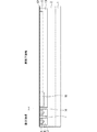
図1は、本開示に係る実施の形態1のn型炭化珪素MOSFET100の上面構成を模式的に示す平面図である。なお、全ての実施の形態においては図1の上面構成は共通である。
次に、n型炭化珪素MOSFET100の製造方法の一例について、製造工程を順に示す断面図である図7〜図18を用いて説明する。
次に、実施の形態1のn型炭化珪素MOSFET100の構成による効果について説明する。n型炭化珪素MOSFET100においては、例えば、図3に示したように、第2ウェルコンタクト領域16は、第2ソースコンタクト17の下方のpn接合部から素子領域側に延在し、第2ソース領域15は、第2ソースコンタクト17の下方のpn接合部から非素子領域側に延在するように設けられている。
図19は、実施の形態2のn型炭化珪素MOSFET200の構成を示す断面図であり、図1におけるA−A線での矢示方向断面図に相当する。図19に示されるようにn型炭化珪素MOSFET200においては、第2ウェルコンタクト領域16の第2ソースコンタクト17の下方のpn接合部から素子領域側に延在する部分が、フィールド絶縁膜28の直下までしか延在せず、境界部ゲート電極19の直下には達していない。
図21は、実施の形態3のn型炭化珪素MOSFET300の素子領域および非素子領域の構成を示す平面図であり、図1における領域Xにおける平面図に相当する。なお、図5と同様、便宜的に、ドリフト層2上の絶縁膜および電極は省略し、ドリフト層2の上層部の構成のみを示している。なお、図21においては、図5を用いて説明した構成と同一の構成については同一の符号を付し、重複する説明は省略する。
図23は、実施の形態4のn型炭化珪素MOSFET400の構成を示す断面図であり、図1におけるA−A線での矢示方向断面図に相当する。図23に示されるようにn型炭化珪素MOSFET400においては、第2ウェルコンタクト領域16の第2ソースコンタクト17の下方のpn接合部から素子領域側に延在する部分が、第2ウェル領域13の端部(第2ウェル領域13端)まで設けられている。
Claims (16)
- 半導体素子が形成された素子領域と、該素子領域以外の非素子領域とを有し、前記素子領域において、炭化珪素基板の厚み方向に主電流が流れる炭化珪素半導体装置であって、
前記炭化珪素基板の第1の主面上に設けられた第1導電型の半導体層と、
前記素子領域の前記半導体層の上層部に設けられた第2導電型の第1ウェル領域と、
前記第1ウェル領域の上層部に設けられた第1導電型の第1不純物領域と、
前記第1ウェル領域の上層部に設けられ、側面において前記第1不純物領域に接合する第2導電型の第1ウェルコンタクト領域と、
前記第1不純物領域の端縁部上、前記第1ウェル領域上および前記半導体層上に設けられたゲート絶縁膜と、
前記ゲート絶縁膜上に設けられたゲート電極と、
前記第1不純物領域および前記第1ウェルコンタクト領域にオーミック接触し、前記半導体層の上方に設けられた第1主電極に電気的に接続される第1コンタクトと、
前記非素子領域の前記半導体層の上層部に設けられた第2導電型の第2ウェル領域と、
前記第2ウェル領域の上層部に設けられた第1導電型の第2不純物領域と、
前記第2ウェル領域の上層部に設けられ、側面において前記第2不純物領域に接合する第2導電型の第2ウェルコンタクト領域と、
前記第2ウェル領域上に設けられたフィールド絶縁膜と、
前記フィールド絶縁膜を貫通して、前記第2不純物領域および前記第2ウェルコンタクト領域にオーミック接触し、前記第1主電極に電気的に接続される少なくとも1つの第2コンタクトと、
前記素子領域と前記非素子領域との境界の側の前記第2不純物領域の端縁部上から、前記境界に隣り合う前記第1ウェル領域内の前記第1不純物領域の端縁部上にかけて設けられた境界部ゲート絶縁膜と、
前記境界部ゲート絶縁膜上に設けられた境界部ゲート電極と、
前記炭化珪素基板の前記第1の主面とは反対側の第2の主面上に設けられた第2主電極と、を備え、
前記第2ウェルコンタクト領域は、前記少なくとも1つの第2コンタクトの下方から前記素子領域側に延在し、
前記第2不純物領域は、前記少なくとも1つの第2コンタクトの下方から前記非素子領域側に延在する、炭化珪素半導体装置。 - 前記少なくとも1つの第2コンタクトは複数の第2コンタクトであって、
前記第2ウェルコンタクト領域は、
平面視で前記複数の第2コンタクトの下方に及ぶように連続的に設けられ、
前記第2不純物領域は、
平面視で複数の第2コンタクトの下方に及ぶように連続的に設けられる、請求項1記載の炭化珪素半導体装置。 - 前記第2ウェルコンタクト領域は、前記少なくとも1つの第2コンタクトの下方から前記境界部ゲート絶縁膜の直下まで延在する、請求項1記載の炭化珪素半導体装置。
- 前記第2ウェルコンタクト領域は、前記少なくとも1つの第2コンタクトの下方から前記境界部ゲート絶縁膜の直下に達しない長さに設けられる、請求項1記載の炭化珪素半導体装置。
- 前記第2ウェルコンタクト領域は、
前記複数の第2コンタクト間において、前記第2不純物領域との接合部から前記素子領域側に延在する部分の長さが、前記少なくとも1つの第2コンタクトの下方の前記第2不純物領域との接合部から前記素子領域側に延在する部分の長さよりも短い、請求項2記載の炭化珪素半導体装置。 - 前記第2ウェルコンタクト領域は、前記少なくとも1つの第2コンタクトの下方から前記素子領域の側の前記第2ウェル領域の端部まで延在する、請求項1記載の炭化珪素半導体装置。
- 前記少なくとも1つの第2ソースコンタクトにオーミック接触する前記第2ウェルコンタクト領域の面積は、前記少なくとも1つの第2ソースコンタクトにオーミック接触する前記第2不純物領域の面積よりも広い、請求項1記載の炭化珪素半導体装置。
- 前記少なくとも1つの第2ソースコンタクトにオーミック接触する前記第2ウェルコンタクト領域の面積は、前記少なくとも1つの第2ソースコンタクトにオーミック接触する前記第2不純物領域の面積の1倍以上100倍以下である、請求項1記載の炭化珪素半導体装置。
- 前記第2不純物領域の第1導電型の不純物濃度は、
1.0×1017cm−3以上1.0×1021cm−3以下である、請求項1記載の炭化珪素半導体装置。 - 前記第2不純物領域の第1導電型の不純物濃度は、
1.0×1019cm−3以上1.0×1020cm−3以下である、請求項1記載の炭化珪素半導体装置。 - 前記第2ウェルコンタクト領域の第2導電型の不純物濃度は、
1.0×1018cm−3以上1.0×1022cm−3以下である、請求項1記載の炭化珪素半導体装置。 - 前記第2ウェルコンタクト領域の第2導電型の不純物濃度は、
1.0×1019cm−3以上1.0×1021cm−3以下である、請求項1記載の炭化珪素半導体装置。 - 前記第2ウェルコンタクト領域は、
前記少なくとも1つの第2コンタクトの下方の前記第2不純物領域との接合部から前記素子領域側に延在する部分の長さが、1.0μm以上100μm以下である、請求項1記載の炭化珪素半導体装置。 - 前記第2不純物領域のシート抵抗値は、前記第2ウェルコンタクト領域のシート抵抗値よりも低い、請求項1記載の炭化珪素半導体装置。
- 前記第2不純物領域と前記少なくとも1つの第2コンタクトとの接触微分抵抗値は、前記第2ウェルコンタクト領域と前記少なくとも1つの第2ソースコンタクトとの接触微分抵抗値よりも低い、請求項1記載の炭化珪素半導体装置。
- 前記第1主電極と前記第2主電極との間に加わる電圧の時間変動は、20V/nsec以上である、請求項1記載の炭化珪素半導体装置。
Applications Claiming Priority (1)
| Application Number | Priority Date | Filing Date | Title |
|---|---|---|---|
| PCT/JP2020/024835 WO2021260853A1 (ja) | 2020-06-24 | 2020-06-24 | 炭化珪素半導体装置 |
Publications (2)
| Publication Number | Publication Date |
|---|---|
| JP6840300B1 true JP6840300B1 (ja) | 2021-03-10 |
| JPWO2021260853A1 JPWO2021260853A1 (ja) | 2021-12-30 |
Family
ID=74845352
Family Applications (1)
| Application Number | Title | Priority Date | Filing Date |
|---|---|---|---|
| JP2020553681A Active JP6840300B1 (ja) | 2020-06-24 | 2020-06-24 | 炭化珪素半導体装置 |
Country Status (5)
| Country | Link |
|---|---|
| US (1) | US20230155021A1 (ja) |
| JP (1) | JP6840300B1 (ja) |
| CN (1) | CN115917755A (ja) |
| DE (1) | DE112020007341T5 (ja) |
| WO (1) | WO2021260853A1 (ja) |
Cited By (1)
| Publication number | Priority date | Publication date | Assignee | Title |
|---|---|---|---|---|
| WO2023042508A1 (ja) * | 2021-09-15 | 2023-03-23 | 住友電気工業株式会社 | 炭化珪素半導体装置 |
Family Cites Families (4)
| Publication number | Priority date | Publication date | Assignee | Title |
|---|---|---|---|---|
| JP4253558B2 (ja) * | 2003-10-10 | 2009-04-15 | 株式会社豊田中央研究所 | 半導体装置 |
| JP5528424B2 (ja) * | 2009-02-24 | 2014-06-25 | 三菱電機株式会社 | 炭化珪素半導体装置 |
| DE112011101254B4 (de) | 2010-04-06 | 2017-04-06 | Mitsubishi Electric Corporation | Leistungshalbleiterbauteile und Verfahren zu deren Herstellung |
| DE112015006322T5 (de) * | 2015-03-18 | 2017-11-30 | Mitsubishi Electric Corporation | Leistungshalbleitervorrichtung |
-
2020
- 2020-06-24 CN CN202080100712.4A patent/CN115917755A/zh active Pending
- 2020-06-24 DE DE112020007341.6T patent/DE112020007341T5/de active Pending
- 2020-06-24 WO PCT/JP2020/024835 patent/WO2021260853A1/ja active Application Filing
- 2020-06-24 JP JP2020553681A patent/JP6840300B1/ja active Active
- 2020-06-24 US US17/917,564 patent/US20230155021A1/en active Pending
Cited By (1)
| Publication number | Priority date | Publication date | Assignee | Title |
|---|---|---|---|---|
| WO2023042508A1 (ja) * | 2021-09-15 | 2023-03-23 | 住友電気工業株式会社 | 炭化珪素半導体装置 |
Also Published As
| Publication number | Publication date |
|---|---|
| DE112020007341T5 (de) | 2023-04-06 |
| JPWO2021260853A1 (ja) | 2021-12-30 |
| WO2021260853A1 (ja) | 2021-12-30 |
| CN115917755A (zh) | 2023-04-04 |
| US20230155021A1 (en) | 2023-05-18 |
Similar Documents
| Publication | Publication Date | Title |
|---|---|---|
| US7791135B2 (en) | Insulated gate silicon carbide semiconductor device and method for manufacturing the same | |
| JP4153811B2 (ja) | 高耐圧半導体装置及びその製造方法 | |
| US6855970B2 (en) | High-breakdown-voltage semiconductor device | |
| JP3721172B2 (ja) | 半導体装置 | |
| JP2008177335A (ja) | 炭化珪素絶縁ゲート型半導体装置。 | |
| WO2011136272A1 (ja) | 半導体装置 | |
| JPH08181313A (ja) | 横型トレンチmisfetおよびその製造方法 | |
| JP5321377B2 (ja) | 電力用半導体装置 | |
| JP5145694B2 (ja) | SiC半導体縦型MOSFETの製造方法。 | |
| WO2017064887A1 (ja) | 半導体装置 | |
| JP4488660B2 (ja) | Mos電界効果トランジスタ | |
| JP7155641B2 (ja) | 半導体装置 | |
| WO2014083771A1 (ja) | 半導体素子及びその製造方法 | |
| JP5556863B2 (ja) | ワイドバンドギャップ半導体縦型mosfet | |
| JP4948784B2 (ja) | 半導体装置及びその製造方法 | |
| WO2015111218A1 (ja) | 半導体装置 | |
| JP6840300B1 (ja) | 炭化珪素半導体装置 | |
| JP2023060183A (ja) | 半導体装置 | |
| TWI760453B (zh) | 半導體裝置之製造方法 | |
| KR101875638B1 (ko) | 반도체 소자 및 그 제조 방법 | |
| JP7486399B2 (ja) | 半導体装置および半導体装置の製造方法 | |
| JP7158317B2 (ja) | 半導体装置 | |
| US20240097050A1 (en) | Semiconductor device and fabrication method thereof | |
| US20240162297A1 (en) | Silicon carbide semiconductor device | |
| US20240170569A1 (en) | Semiconductor device and method of manufacturing the same |
Legal Events
| Date | Code | Title | Description |
|---|---|---|---|
| A621 | Written request for application examination |
Free format text: JAPANESE INTERMEDIATE CODE: A621 Effective date: 20201001 |
|
| A871 | Explanation of circumstances concerning accelerated examination |
Free format text: JAPANESE INTERMEDIATE CODE: A871 Effective date: 20201001 |
|
| A975 | Report on accelerated examination |
Free format text: JAPANESE INTERMEDIATE CODE: A971005 Effective date: 20201111 |
|
| TRDD | Decision of grant or rejection written | ||
| A01 | Written decision to grant a patent or to grant a registration (utility model) |
Free format text: JAPANESE INTERMEDIATE CODE: A01 Effective date: 20210119 |
|
| A61 | First payment of annual fees (during grant procedure) |
Free format text: JAPANESE INTERMEDIATE CODE: A61 Effective date: 20210216 |
|
| R150 | Certificate of patent or registration of utility model |
Ref document number: 6840300 Country of ref document: JP Free format text: JAPANESE INTERMEDIATE CODE: R150 |
|
| R250 | Receipt of annual fees |
Free format text: JAPANESE INTERMEDIATE CODE: R250 |