WO2021200197A1 - 電解コンデンサ - Google Patents
電解コンデンサ Download PDFInfo
- Publication number
- WO2021200197A1 WO2021200197A1 PCT/JP2021/011000 JP2021011000W WO2021200197A1 WO 2021200197 A1 WO2021200197 A1 WO 2021200197A1 JP 2021011000 W JP2021011000 W JP 2021011000W WO 2021200197 A1 WO2021200197 A1 WO 2021200197A1
- Authority
- WO
- WIPO (PCT)
- Prior art keywords
- main surface
- external electrode
- exterior body
- anode
- electrolytic capacitor
- Prior art date
- Legal status (The legal status is an assumption and is not a legal conclusion. Google has not performed a legal analysis and makes no representation as to the accuracy of the status listed.)
- Ceased
Links
Images


Classifications
-
- H—ELECTRICITY
- H01—ELECTRIC ELEMENTS
- H01G—CAPACITORS; CAPACITORS, RECTIFIERS, DETECTORS, SWITCHING DEVICES, LIGHT-SENSITIVE OR TEMPERATURE-SENSITIVE DEVICES OF THE ELECTROLYTIC TYPE
- H01G9/00—Electrolytic capacitors, rectifiers, detectors, switching devices, light-sensitive or temperature-sensitive devices; Processes of their manufacture
- H01G9/15—Solid electrolytic capacitors
-
- H—ELECTRICITY
- H01—ELECTRIC ELEMENTS
- H01G—CAPACITORS; CAPACITORS, RECTIFIERS, DETECTORS, SWITCHING DEVICES, LIGHT-SENSITIVE OR TEMPERATURE-SENSITIVE DEVICES OF THE ELECTROLYTIC TYPE
- H01G4/00—Fixed capacitors; Processes of their manufacture
- H01G4/30—Stacked capacitors
-
- H—ELECTRICITY
- H01—ELECTRIC ELEMENTS
- H01G—CAPACITORS; CAPACITORS, RECTIFIERS, DETECTORS, SWITCHING DEVICES, LIGHT-SENSITIVE OR TEMPERATURE-SENSITIVE DEVICES OF THE ELECTROLYTIC TYPE
- H01G9/00—Electrolytic capacitors, rectifiers, detectors, switching devices, light-sensitive or temperature-sensitive devices; Processes of their manufacture
- H01G9/004—Details
- H01G9/008—Terminals
- H01G9/012—Terminals specially adapted for solid capacitors
-
- H—ELECTRICITY
- H01—ELECTRIC ELEMENTS
- H01G—CAPACITORS; CAPACITORS, RECTIFIERS, DETECTORS, SWITCHING DEVICES, LIGHT-SENSITIVE OR TEMPERATURE-SENSITIVE DEVICES OF THE ELECTROLYTIC TYPE
- H01G9/00—Electrolytic capacitors, rectifiers, detectors, switching devices, light-sensitive or temperature-sensitive devices; Processes of their manufacture
- H01G9/004—Details
- H01G9/04—Electrodes or formation of dielectric layers thereon
- H01G9/042—Electrodes or formation of dielectric layers thereon characterised by the material
-
- H—ELECTRICITY
- H01—ELECTRIC ELEMENTS
- H01G—CAPACITORS; CAPACITORS, RECTIFIERS, DETECTORS, SWITCHING DEVICES, LIGHT-SENSITIVE OR TEMPERATURE-SENSITIVE DEVICES OF THE ELECTROLYTIC TYPE
- H01G9/00—Electrolytic capacitors, rectifiers, detectors, switching devices, light-sensitive or temperature-sensitive devices; Processes of their manufacture
- H01G9/004—Details
- H01G9/04—Electrodes or formation of dielectric layers thereon
- H01G9/048—Electrodes or formation of dielectric layers thereon characterised by their structure
- H01G9/052—Sintered electrodes
-
- H—ELECTRICITY
- H01—ELECTRIC ELEMENTS
- H01G—CAPACITORS; CAPACITORS, RECTIFIERS, DETECTORS, SWITCHING DEVICES, LIGHT-SENSITIVE OR TEMPERATURE-SENSITIVE DEVICES OF THE ELECTROLYTIC TYPE
- H01G9/00—Electrolytic capacitors, rectifiers, detectors, switching devices, light-sensitive or temperature-sensitive devices; Processes of their manufacture
- H01G9/004—Details
- H01G9/04—Electrodes or formation of dielectric layers thereon
- H01G9/048—Electrodes or formation of dielectric layers thereon characterised by their structure
- H01G9/055—Etched foil electrodes
-
- H—ELECTRICITY
- H01—ELECTRIC ELEMENTS
- H01G—CAPACITORS; CAPACITORS, RECTIFIERS, DETECTORS, SWITCHING DEVICES, LIGHT-SENSITIVE OR TEMPERATURE-SENSITIVE DEVICES OF THE ELECTROLYTIC TYPE
- H01G9/00—Electrolytic capacitors, rectifiers, detectors, switching devices, light-sensitive or temperature-sensitive devices; Processes of their manufacture
- H01G9/004—Details
- H01G9/08—Housing; Encapsulation
- H01G9/10—Sealing, e.g. of lead-in wires
Definitions
- This disclosure relates to electrolytic capacitors.
- the electrolytic capacitor includes a capacitor element, an exterior body that seals the capacitor element, and external electrodes that are electrically connected to the anode side and the cathode side of the capacitor element, respectively.
- the capacitor element includes an anode having a first portion (also referred to as an anode extraction portion) including a first end portion and a second portion (also referred to as a cathode forming portion) including a second end portion, and at least a second portion of the anode body.
- a dielectric layer formed on the surface of the dielectric layer and a cathode portion covering at least a part of the dielectric layer are provided.
- Patent Document 1 describes a solid having an element laminate in which flat-plate capacitor elements having an anode electrode portion and a cathode electrode portion are laminated in even-numbered units so that the anode electrode portions are alternately arranged in opposite directions. Electrode capacitors have been proposed.
- the solid electrolytic capacitor of Patent Document 1 consists of a pair of anode comb terminals joined so as to integrally bond the anode electrode portions located at both ends of the element laminate, and a cathode electrode portion located in the center of the element laminate.
- a cathode comb terminal bonded to the lower surface, a pair of anode terminals provided on the lower surfaces of the pair of anode comb terminals, and a pair of cathode terminals bonded to the cathode comb terminal are further provided.
- the pair of anode terminals are connected to each other by a plate-shaped inductor portion, and the pair of cathode terminals are joined to both ends of the lower surface of the cathode comb terminal in the direction intersecting the inductor portion.
- Patent Document 1 proposes a low ESL (equivalent series inductance) of an electrolytic capacitor by this configuration.
- the electrolytic capacitor according to one aspect of the present disclosure includes a capacitor element, an exterior body for sealing the capacitor element, a first external electrode, and a second external electrode, and the capacitor element is the first.
- the exterior body has a solid electrolyte layer that covers the surface and is electrically connected to the second external electrode, and the exterior body has a first main surface and a second main surface that intersects the first main surface.
- a third main surface opposite to the first main surface and a fourth main surface opposite to the second main surface, the first external electrode and the second external electrode. Are formed so as to be separated from each other along the first main surface of the exterior body. According to the present disclosure, a high capacity can be realized while keeping the ESL of the electrolytic capacitor low.
- FIG. 1 is a perspective view schematically showing an electrolytic capacitor according to the first embodiment of the present disclosure.
- FIG. 2 is a bottom view schematically showing an electrolytic capacitor according to the first embodiment of the present disclosure.
- FIG. 3A is a cross-sectional view schematically showing the structure of the electrolytic capacitor according to the first embodiment of the present disclosure.
- FIG. 3B is a cross-sectional view schematically showing the structure of the electrolytic capacitor according to the first embodiment of the present disclosure.
- FIG. 3C is a cross-sectional view schematically showing the structure of the electrolytic capacitor according to the first embodiment of the present disclosure.
- FIG. 4 is a diagram showing an example of the layout of the capacitor element used in the electrolytic capacitor according to the first embodiment of the present disclosure.
- FIG. 5 is a diagram showing an example of the shape of the cathode foil used for the electrolytic capacitor according to the first embodiment of the present disclosure.
- FIG. 6 is a table showing an example of how to combine the anode foil and the cathode foil used in the electrolytic capacitor according to the first embodiment of the present disclosure.
- FIG. 7 is a table showing an example of how to combine the anode foil and the cathode foil used in the electrolytic capacitor according to the first embodiment of the present disclosure.
- FIG. 8 is a table showing an example of how to combine the anode foil and the cathode foil used in the electrolytic capacitor according to the first embodiment of the present disclosure.
- FIG. 9 is a table showing an example of how to combine the anode foil and the cathode foil used in the electrolytic capacitor according to the first embodiment of the present disclosure.
- FIG. 10 is a perspective view schematically showing an electrolytic capacitor according to a second embodiment of the present disclosure.
- FIG. 11 is a table showing an example of how to combine the anode foil and the cathode foil used in the electrolytic capacitor according to the second embodiment of the present disclosure.
- FIG. 12 is a table showing an example of how to combine the anode foil and the cathode foil used in the electrolytic capacitor according to the second embodiment of the present disclosure.
- FIG. 13 is a perspective view schematically showing another example of the electrolytic capacitor according to the second embodiment of the present disclosure.
- the present disclosure provides an electrolytic capacitor capable of achieving a high capacity while keeping the ESL low.
- the electrolytic capacitor according to the present embodiment includes a capacitor element, an exterior body for sealing the capacitor element, a first external electrode, and a second external electrode.
- the capacitor element includes an anode that is electrically connected to the first external electrode (anode electrode) and has a porous portion on the surface, and a dielectric layer formed on the surface of at least a part of the porous portion. It has a solid electrolyte layer that covers at least a part of the dielectric layer.
- the solid electrolyte layer is electrically connected to the second external electrode (cathode electrode) via the cathode layer (for example, the cathode foil).
- the anode has a flat shape with two main surfaces as a whole.
- the exterior body may have, for example, four main surfaces intersecting the main surfaces of the anode body.
- the four main surfaces are usually planes substantially perpendicular to the main surface of the anode body.
- One of the four main surfaces is the first main surface.
- the four main surfaces are the second main surface that intersects the first main surface, the third main surface on the opposite side of the first main surface, and the second main surface on the opposite side of the second main surface. It may consist of four main surfaces.
- the anode body has an exposed end face on at least the first main surface of the first to fourth main surfaces, and the first external electrode can be electrically connected to the exposed end face of the anode body.
- the first external electrode and the second external electrode are formed so as to be separated from each other at least along the first main surface. That is, both the anode body and the cathode layer are drawn out on the first main surface and are electrically connected to each of the first external electrode and the second external electrode. As a result, the separation distance between the first external electrode and the second external electrode can be shortened as compared with the conventional configuration in which the first external electrode and the second external electrode are provided on the main surfaces facing each other, and the ESL Can be reduced.
- a plurality of first external electrodes may be provided. In that case, at least two of the plurality of first external electrodes are formed so as to be separated from each other along the first main surface of the exterior body. Similarly, it may have a plurality of second external electrodes. ESL can be further reduced by forming the first external electrode and / or the second external electrode by a plurality of separated external electrodes.
- the second external electrode may be interposed between the two separated first external electrodes along the first main surface of the exterior body. This further reduces ESL.
- At least one of the plurality of first external electrodes may be formed along the second main surface. At least one of the plurality of first external electrodes may be formed along the third main surface or the fourth main surface.
- the number of the first external electrode and the number of the second external electrode may be plural.
- at least one of the first external electrodes and at least one of the second external electrodes are formed so as to be separated from each other along the first main surface of the exterior body, and the first external electrode and the second external electrode are formed.
- the rest of the external electrodes can be formed apart from each other along any of the second to fourth main surfaces of the exterior.
- the remaining one of the first external electrodes and the remaining one of the second external electrodes may be formed so as to be separated from each other along the third main surface of the exterior body.
- At least one of the first external electrodes may be formed along the second main surface, and at least one of the second external electrodes may be formed along the fourth main surface. At least one of the first external electrodes and at least one of the second external electrodes may both be formed along the second main surface.
- the distance between the first main surface and the third main surface may be shorter or longer than the distance between the second main surface and the fourth main surface.
- the first main surface and the third main surface correspond to the short side of the contour line of the exterior body which is substantially rectangular
- the second main surface and the fourth main surface correspond to the long side of the contour line of the exterior body which is substantially rectangular. handle.
- at least one first external electrode and at least one second external electrode may be provided on the first main surface as the short side.
- first external electrodes and a plurality of second external electrodes When a plurality of first external electrodes and a plurality of second external electrodes are provided, at least one of the remaining first external electrodes and at least one of the remaining second external electrodes are similarly placed on the opposite side of the first main surface. It may be provided on the third main surface which is the short side.
- the anode body has, for example, a first region covered with a solid electrolyte layer and a second region protruding from the first region and not covered with a solid electrolyte layer at least in a part of the region.
- the second region corresponds to the anode extraction portion.
- the thickness of the porous portion in the height direction in the protruding second region may be thinner than the thickness in the height direction of the porous portion in the first region covered with the solid electrolyte layer.
- the thickness in the height direction may be reduced by pressing or laser irradiation. It is preferable that the thickness of the porous portion in the protruding second region in the height direction of the portion electrically connected to the first external electrode is reduced.
- the protruding second region may consist only of a core portion having no porous portion on the surface.
- a cathode foil electrically connected to the solid electrolyte layer is provided, and the cathode foil is electrically connected to the second external electrode.
- the cathode foil has, for example, a third region facing the solid electrolyte layer and a fourth region protruding from the third region. The fourth region corresponds to the cathode extraction portion. The protruding fourth region is electrically connected to the second external electrode to form a second external electrode along the first main surface (or the second to fourth main surfaces).
- the end face of the fourth region is exposed on the first main surface (or the second to fourth main surfaces) of the exterior body, and the second outer surface is exposed on the exposed end face of the fourth region of the cathode foil. It can be electrically connected to the electrodes.
- the electrolytic capacitor may include a plurality of the above-mentioned capacitor elements.
- the electrolytic capacitor includes an element laminate in which capacitor elements are laminated.
- a cathode foil is interposed between adjacent capacitor elements.
- the plurality of capacitor elements may include at least one first capacitor element and / or a second capacitor element as defined below.
- the anode body is electrically connected to the first external electrode on at least one of the first main surface and the third main surface of the exterior body.
- the cathode foil is electrically connected to the second external electrode on at least one of the first main surface and the third main surface.
- the anode body is electrically connected to the first external electrode on only one of the first main surface and the third main surface of the exterior body.
- the cathode foil is electrically connected to the second external electrode on only one of the first main surface and the third main surface.
- An electrolytic capacitor can be configured by using an element laminate in which first and second capacitor elements are alternately laminated.
- the first capacitor element one in which the anode body is electrically connected to the first external electrode only on the first main surface of the first main surface and the third main surface of the exterior body is used, and the first capacitor element is used.
- the capacitor element 2 an anode body that is electrically connected to the first external electrode only on the third main surface of the first main surface and the third main surface of the exterior body can be used.
- the first and second capacitor elements are alternately laminated, the first main surface and the third main surface are surfaces facing each other of the exterior body, so that the first capacitor element and the second capacitor element
- the direction of the current flowing through the anode can be opposite.
- the direction of the magnetic field generated by the current flowing through the anode body is different, so that the magnetic flux generated in the device stack is reduced. Thereby, ESL can be further reduced.
- first main surface and the third main surface only the first main surface (third main surface) is electrically connected to the external electrode, whichever is the first main surface or the third main surface. It means that it is electrically connected to the external electrode on one side and not electrically connected to the external electrode on the other side, and is electrically connected to the external electrode on the second main surface and / or the fourth main surface as described later. It does not exclude the case of being connected as a target.
- the cathode foil in the first capacitor element one that is electrically connected to the second external electrode on either the first main surface or the third main surface may be used.
- the cathode foil in the second condenser element one that is electrically connected to the second external electrode on the side opposite to the first condenser element may be used. That is, when the cathode foil in the second condenser element is electrically connected to the second external electrode on the first main surface, the cathode foil in the first capacitor element is on the third main surface or on the first main surface.
- the cathode foil in the capacitor element is electrically connected to the second external electrode on the third main surface, it may be electrically connected to the second external electrode on the first main surface.
- the directions of the currents flowing through the cathode foil may be opposite between the first capacitor element and the second capacitor element.
- the direction of the magnetic field generated by the current flowing through the cathode foil is different, so that the magnetic flux generated in the device stack is reduced. Thereby, ESL can be further reduced.
- the anode body is electrically connected to the first external electrode only on the first main surface of the first and third main surfaces of the exterior body, and the cathode foil is the exterior body. Only the third main surface of the first main surface and the third main surface may be electrically connected to the second external electrode.
- the anode body is electrically connected to the first external electrode only on the third main surface of the first and third main surfaces of the exterior body, and the cathode foil is the exterior body. Of the first main surface and the third main surface, only the first main surface may be electrically connected to the second external electrode.
- the first external electrode may be provided along the second main surface and / or the fourth main surface of the exterior body.
- the first capacitor element one in which the anode body is electrically connected to the first external electrode on one main surface of the second main surface and the fourth main surface of the exterior body is used, and the first capacitor element is used.
- an anode body may be used in which the anode body is electrically connected to the first external electrode on the other main surface of the second main surface and the fourth main surface of the exterior body.
- the second main surface and the fourth main surface are surfaces facing each other of the exterior body, so that the first capacitor element and the second capacitor element
- the direction of the current flowing through the anode can be opposite.
- the direction of the magnetic field generated by the current flowing through the anode body is different, so that the magnetic flux generated in the device stack is reduced. Thereby, ESL can be further reduced.
- the second external electrode may be provided along the second main surface and / or the fourth main surface of the exterior body.
- the first capacitor element one in which the cathode foil is electrically connected to the second external electrode on one of the second main surface and the fourth main surface of the exterior body is used, and the first capacitor element is used.
- the capacitor element 2 an element in which the cathode foil is electrically connected to the second external electrode on the second main surface and the other main surface of the fourth main surface of the exterior body may be used.
- the second main surface and the fourth main surface are surfaces facing each other of the exterior body, so that the first capacitor element and the second capacitor element
- the direction of the current flowing through the cathode foil can be opposite.
- the direction of the magnetic field generated by the current flowing through the cathode foil is different, so that the magnetic flux generated in the device stack is reduced.
- ESL can be further reduced.
- the anode body is electrically connected to the first external electrode only on the second main surface of the second and fourth main surfaces of the exterior body, and the cathode foil is the exterior body. Of the second main surface and the fourth main surface, only the fourth main surface may be electrically connected to the second external electrode.
- the anode body is electrically connected to the first external electrode only on the fourth main surface of the second and fourth main surfaces of the exterior body, and the cathode foil is the exterior body. Of the second main surface and the fourth main surface, only the second main surface may be electrically connected to the second external electrode.
- the first capacitor element and / or the second capacitor element having different electrical connection points with the first external electrode and / or the second external electrode are alternately laminated, thereby forming the element laminate.
- the resulting magnetic flux can be effectively reduced. Therefore, ESL can be effectively reduced.
- the number of the first capacitor and the number of the second capacitor may be the same.
- the magnetic field generated by the current flowing through the anode body of the first capacitor element and the magnetic field generated by the current flowing through the anode body of the second capacitor element are excessive. They cancel each other out without any shortage, and the magnetic flux generated in the element stack is reduced. Therefore, it is easy to reduce ESL.
- the end face of the second region of the anode body exposed from the exterior body of each capacitor element is electrically connected to the first external electrode.
- this can be done by electrically connecting the end face of the fourth region of the cathode foil exposed from the outer body of each capacitor element to the second external electrode.
- the electrical connection between each end face and the external electrode is made by using the external electrode formed along the first to fourth main surfaces of the exterior body, or in the middle formed along the first to fourth main surfaces. This can be done by electrically connecting the electrodes to the external electrodes. In this case, since it is not necessary to interpose another member for connecting the second region and the fourth region to the external electrode in the outer body, it is easy to increase the capacity of the electrolytic capacitor.
- the cathode foil is, for example, a metal foil, and may be a vapor-deposited foil or a coated foil in which the surface of the metal foil (for example, Al foil or copper foil) is coated with a conductive film by vapor deposition or coating.
- the conductive film include Ti and its nitrides, carbides, carbonitrides, oxides, and C (carbon) films.
- the vapor deposition film may be nickel.
- the metal foil may be a plain foil or an etching foil.
- the first main surface and the third main surface may be surfaces parallel to the longitudinal direction of the exterior body, or may be surfaces parallel to the lateral direction of the exterior body.
- the first external electrode and the second external electrode may be provided along a plane parallel to the longitudinal direction of the anode body. That is, in the exterior body, the separation distance between the first main surface and the third main surface on which the external electrodes are formed may be shorter than the separation distance between the second main surface and the fourth main surface. ..
- the first external electrode and the second external electrode may each extend from the corresponding main surface along the bottom surface of the electrolytic capacitor.
- the anode terminal and / or the cathode terminal can be provided on the bottom surface of the electrolytic capacitor.
- the current flowing in the extending portion of the first external electrode flows in the direction opposite to the current flowing in the second region (anode extraction portion) electrically connected to the first external electrode.
- the current flowing through the extending portion of the second external electrode flows in the direction opposite to the fourth region (cathode extraction portion) electrically connected to the second external electrode.
- the magnetic field generated by the current flowing in the second region is canceled by the magnetic field generated by the current flowing in the extending portion of the first external electrode, and / or the magnetic field generated by the current flowing in the fourth region is generated by the second region.
- the ESL of the electrolytic capacitor can be further reduced by being canceled by the magnetic field generated by the current flowing through the extending portion of the external electrode.
- ESL is reduced by having a plurality of first external electrodes and / or second external electrodes.
- first external electrodes When a plurality of first external electrodes are provided, at least two of the first external electrodes may be separated from each other along the same main surface among the first to fourth main surfaces.
- second external electrodes When a plurality of second external electrodes are provided, at least two of the second external electrodes may be separated from each other along the same main surface of the first to fourth main surfaces.
- a second external electrode is interposed between two first external electrodes arranged along the same main surface, and / or two second external electrodes arranged along the same main surface.
- a first external electrode may be interposed between them. In this case, it is easy to reduce ESL.
- the element laminate is supported on a substrate, for example, to form an electrolytic capacitor.
- the substrate is not particularly limited as long as it can electrically separate the first external electrode and the second external electrode.
- a substrate having a wiring layer formed on its surface may be used. In that case, the wiring layer may be electrically connected to the solid electrolyte layer.
- a wiring layer (third external electrode) may also be formed on the back surface of the substrate.
- the third external electrode may be electrically connected to the wiring layer on the surface of the substrate, for example, via a via hole.
- the third external electrode functions as a cathode terminal of the electrolytic capacitor.
- the third external electrode may be electrically connected to the second external electrode that also constitutes the cathode terminal.
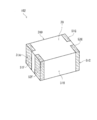
- FIG. 1 is a perspective view schematically showing an electrolytic capacitor 100 according to an embodiment of the present disclosure.
- FIG. 2 is a view of the electrolytic capacitor 100 as viewed from the bottom surface.
- Figure 3A ⁇ C respectively, X 1 -X 2 direction in FIG. 2 of the electrolytic capacitor 100, Y 1 -Y 2 direction, and a cross-sectional view showing a structure of Y 3 -Y 4 directions.
- the electrolytic capacitor according to the present invention is not limited to these.
- the electrolytic capacitor 100 can be manufactured by using the anode foil and the cathode foil shown in the configuration example 3 of FIG. 6 to be described later.
- the electrolytic capacitor 100 includes an anode foil 10 which is an anode body, a solid electrolyte layer 7, and a cathode foil 20.
- the anode foil 10 and the cathode foil 20 are alternately laminated with the solid electrolyte layer 7 interposed therebetween.
- One capacitor element 40 (first or second capacitor element) is formed by the solid electrolyte layer 7 and the anode foils 10 facing each other with the solid electrolyte layer 7 interposed therebetween.
- the electrolytic capacitor 100 includes an element laminate in which a plurality of capacitor elements 40 are laminated.
- a cathode foil 20 is interposed between adjacent capacitor elements in the stacking direction.
- the element laminate is supported by the substrate 24.
- the substrate may be, for example, an insulating substrate, or a metal substrate or a wiring pattern as long as the first external electrodes 51A to 51E and the second external electrodes 52A to 52E can be electrically separated. It may be a printed circuit board that has been applied.
- the anode foil 10 has a porous portion 5 on the surface, and a dielectric layer (not shown) is formed on the surface of at least a part of the porous portion 5.
- the solid electrolyte layer 7 covers at least a part of the dielectric layer.
- the anode foil 10 has a region covered with the solid electrolyte layer 7 and a region not covered with the solid electrolyte layer 7.
- the anode foil 10 has an end portion 1, and at least a part of the end face side of the end portion 1 is not covered with the solid electrolyte layer, but is covered with the insulating film 8 instead.
- the region of the end portion 1 of the anode foil 10 that is not covered with the solid electrolyte layer is also referred to as the anode extraction portion.
- the region of the anode foil 10 covered with the solid electrolyte layer 7 is also referred to as a cathode forming portion.
- the anode foil 10 has a core portion 4 and a porous portion (porous body) 5 formed on the surface of the core portion 4 by roughening (etching or the like) or the like in the cathode forming portion.
- the anode extraction portion may or may not have the porous portion 5 on the surface.
- the dielectric layer is formed along the surface of the porous portion 5. At least a part of the dielectric layer covers the inner wall surface of the pore of the porous portion 5 and is formed along the inner wall surface thereof.
- the surface of the dielectric layer is formed with an uneven shape corresponding to the shape of the surface of the porous portion 5, and the solid electrolyte layer 7 can be formed so as to fill the unevenness of the dielectric layer.
- An adhesive layer 23 is interposed between the cathode foil 20 and the solid electrolyte layer 7.
- the cathode foil 20 covers at least a part of the solid electrolyte layer 7 via the adhesive layer 23.
- the cathode foil 20, the solid electrolyte layer 7, and the adhesive layer 23 form a cathode portion.
- the adhesive layer 23 is, for example, a carbon paste or a silver paste.
- a conductive layer may be formed between the solid electrolyte layer 7 and the adhesive layer 23 in order to enhance the electrical connectivity between the solid electrolyte layer 7 and the adhesive layer 23 and enhance the current collecting property.
- the conductive layer is, for example, a carbon layer and contains conductive carbon particles.
- the conductive layer may be formed so as to cover the solid electrolyte layer 7.
- the adhesive layer 23 and the conductive layer form a cathode layer and have an effect of enhancing the current collecting property of the element.
- the cathode foil 20 acts as a lead for pulling out the cathode layer and connecting it to the external electrode.
- the conductive layer may have a laminated structure of a carbon layer covering the solid electrolyte layer 7 and a silver paste layer covering the carbon layer.
- the adhesive layer 23 may be formed so as to cover the conductive layer.
- the cathode foil 20 has a region facing the solid electrolyte layer 7 and a region not facing the solid electrolyte layer 7.
- the cathode foil 20 has an end portion 2, and the end portion 2 is not covered with the solid electrolyte layer 7, and the surface of the cathode foil 20 is exposed.
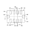
- the electrolytic capacitor 100 includes the above-mentioned element laminate in which a plurality of capacitor elements 40 are laminated, an exterior body 30 that seals the element laminate, first external electrodes 51A to 51E, and second external electrodes 52A to 52A. 52E and.
- the first external electrodes 51A to 51E are the anodes of the electrolytic capacitor 100
- the second external electrodes 52A to 52E are the cathodes of the electrolytic capacitor 100.
- the first external electrodes 51A to 51E and the second external electrodes 52A to 52E formed apart from each other constitute an electrolytic capacitor 100 having 10 terminals.
- the exterior body 30 has a substantially rectangular parallelepiped outer shape, and the electrolytic capacitor 100 also has a substantially rectangular parallelepiped outer shape.
- the exterior body 30 has four main surfaces 31A to 31D perpendicular to the main surface of the anode foil 10.
- the second main surface 31B and the fourth main surface 31D are surfaces that intersect the first main surface 31A.
- the third main surface 31C is located on the opposite side of the first main surface 31A.
- the fourth main surface 31D is located on the opposite side of the second main surface 31B.
- the first external electrodes 51A and 51B and the second external electrodes 52A and 52B are provided along the first main surface 31A.
- the first external electrodes 51C and 51D and the second external electrodes 52C and 52D are provided along the third main surface 31C.
- the first external electrode 51E is provided along the fourth main surface 31D, and the second external electrode 52E is provided along the second main surface 31B.
- the end surface 3A of the end portion 1 of the anode foil 10 is exposed from the exterior body 30 on the first main surface 31A, the third main surface 31C, and the fourth main surface 31D, and is electrically connected to the first external electrodes 51A to 51E. Is connected to.
- the end surface 3B of the end portion 2 of the cathode foil 20 is exposed from the exterior body 30 on the first main surface 31A, the second main surface 31B, and the third main surface 31C, and becomes the second external electrodes 52A to 52E. It is electrically connected.
- a first external electrode may be separately provided along the second main surface 31B and electrically connected to the end surface 3A of the end portion 1 of the anode foil 10.
- a second external electrode may be separately provided along the fourth main surface 31D and electrically connected to the end surface 3B of the end portion 2 of the cathode foil 20.
- each of the anode foils 10 is electrically connected to at least one of the first external electrodes 51A to 51E extending along any of the first to fourth main surfaces on the end surface 3A. Be connected. Further, each of the cathode foils 20 is electrically connected to at least one of the second external electrodes 52A to 52E extending along any of the first to fourth main surfaces on the end surface 3B.
- the ratio of the end portion 1 to the anode body can be reduced to increase the capacity. Also, the contribution of ESL by the end 1 is reduced.
- first external electrodes 51A and 51B and the second external electrodes 52A and 52B are arranged so that the first external electrode and the second external electrode are alternately arranged.
- first external electrodes 51C and 51D and the second external electrodes 52C and 52D are arranged so that the first external electrode and the second external electrode are alternately arranged.
- the separation distance between the first external electrode which is the anode and the second external electrode which is the cathode can be shortened, and the ESL can be reduced.
- the end face 3A of the end 1 of the anode foil 10 exposed from the exterior body 30 and the end face 3B of the end 2 of the cathode foil 20 are each covered with the contact layer 53.
- the intermediate electrode layer 54 covers a part of the contact layer 53 and the corresponding main surfaces 31A to 31D of the exterior body 30.
- the first external electrodes 51A to 51E and the second external electrodes 52A to 52E respectively cover the corresponding intermediate electrode layer 54.
- Each of the first external electrodes 51A to 51E and the second external electrodes 52A to 52E bends inward along the bottom surface of the exterior body 30 and is exposed on the bottom surface of the electrolytic capacitor 100.
- the exposed portion on the bottom surface of the first external electrodes 51A to 51E constitutes the anode terminal of the electrolytic capacitor.
- the exposed portion on the bottom surface of the second external electrodes 52A to 52E constitutes the cathode terminal of the electrolytic capacitor. That is, in the present embodiment, the electrolytic capacitor 100 has five separated anode terminals and five separated cathode terminals.
- two anode terminals and two cathode terminals are provided along the same side on the bottom surface of the electrolytic capacitor 100, and the anode terminals and the cathode terminals are alternately arranged along the sides.
- the separation distance between the anode terminal and the cathode terminal can be shortened and the ESL can be reduced as compared with the conventional configuration in which the anode terminal and the cathode terminal are provided along the opposite sides of the bottom surface of the electrolytic capacitor 100.
- the capacitor element 40 may have a first capacitor element 40A and a second capacitor element 40B.
- the first capacitor element 40A the end surface 3A of the end portion 1 of the anode foil 10 is exposed from the exterior body 30 on the first main surface 31A and not exposed from the exterior body 30 on the third main surface 31C (FIG. 6). See 3C).
- the second condenser element 40B the end surface 3A of the end portion 1 of the anode foil 10 is exposed from the exterior body 30 on the third main surface 31C, and is not exposed from the exterior body 30 on the first main surface 31A. (See FIG. 3B).
- the direction of the current flowing through the anode foil of the first capacitor element 40A and the second capacitor element 40B is opposite in the normal direction of the first main surface 31A or the third main surface 31C. Therefore, the magnetic field generated by the current flowing through the first capacitor element 40A and the magnetic field generated by the current flowing through the second capacitor element 40B cancel each other out, and the magnetic flux generated by the electrolytic capacitor 100 is reduced. As a result, ESL is reduced.
- the cathode foil 20 may have a first cathode foil and a second cathode foil.
- the first cathode foil is located at the top layer and the third layer from the top of the layered element laminate.
- the end surface 3B of the end portion 2 of the cathode foil 20 is exposed from the exterior body 30 on the first main surface 31A and not exposed from the exterior body 30 on the third main surface 31C (FIG. 3B). reference).
- the second cathode foil is located in the second layer and the lowest layer from the top of the laminated element laminate.
- the end surface 3B of the end portion 2 of the cathode foil 20 is exposed from the exterior body 30 on the third main surface 31C and not exposed from the exterior body 30 on the first main surface 31A (FIG. 3C). reference).
- the first cathode foil and the second cathode foil can be alternately laminated to form the electrolytic capacitor 100.
- the directions of the currents flowing through the cathode foil are opposite in the normal direction of the first main surface 31A or the third main surface 31C. Therefore, the magnetic field generated by the current flowing through the first cathode foil and the magnetic field generated by the current flowing through the second cathode foil cancel each other out, and the magnetic flux generated in the electrolytic capacitor 100 is reduced. As a result, ESL is reduced.
- It can be manufactured by a manufacturing method including a sixth step of electrically connecting the cathode foil to the second external electrode and electrically connecting the end face of the cathode foil to the second external electrode.
- the first step has, for example, the following steps (i) to (iii): (I) A step of preparing an anode foil having a porous portion formed on the surface, (Ii) A step of forming a dielectric layer on the surface of the anode foil, and (Iii) A step of covering at least a part of the anode foil with a solid electrolyte layer.
- the anode foil is processed into a shape having a first region and a second region protruding from the first region.
- the processing is performed, for example, by cutting a large-sized anode foil into a predetermined shape.
- the processing may be performed before each of the steps (i) to (iii), may be performed after each step, or may be performed at any time in the first step.
- FIG. 4 shows an example of the layout of the capacitor element prepared in the first step as viewed from the main surface of the anode body.
- the anode foil 10 has a first region A 1 and a second region A 2 protruding from the first region A 1 .
- the first area A 1 the entire surface is covered by the solid electrolyte layer 7.
- the solid electrolyte layer 7 is not formed. At least at the end portion of the protruding direction of the second region A 2, the solid electrolyte layer 7 may if it is not formed.
- the end faces of the anode foil 10 is exposed from the outer package, an electrical connection between the first external electrode is performed.
- an anode foil having a porous portion formed on its surface is prepared.
- the anode foil can include a valve acting metal, an alloy containing a valve acting metal, a compound containing a valve acting metal (intermetallic compound, etc.) and the like. These materials can be used alone or in combination of two or more.
- the valve acting metal aluminum, tantalum, niobium, titanium and the like can be used.
- the anode foil may be a valve-acting metal, an alloy containing a valve-acting metal, or a foil of a compound containing a valve-acting metal, and is porous of a valve-acting metal, an alloy containing a valve-acting metal, or a compound containing a valve-acting metal. It may be a quality sintered body (sintered foil).
- a porous portion is usually formed in order to increase the surface area.
- the porous portion may be formed on the entire surface of the anode foil, a part of the predetermined region of the surface of the anode foil (e.g., the first region A 1) may be formed on.
- the porous portion may be formed by roughening the entire surface of the surface of the anode foil by etching or the like.
- a roughening treatment such as an etching treatment.
- the etching treatment a known method may be used, and examples thereof include electrolytic etching.
- the masking member is not particularly limited, but an insulator such as resin is preferable. The masking member needs to be removed before forming the solid electrolyte layer, but may be a conductive material.
- the porous portion is formed in the second area A 2, instead of the adhesion of the porous portion and the exterior body is sufficiently inside the electrolytic capacitor through the contact portion between the porous part and the outer body air (specifically May be invaded by oxygen and moisture).
- the second area A 2 do not form a porous portion high to maintain the adhesion between the anode foil and the exterior body, the electrolytic capacitor inside through the porous portion from the second area A 2 exposed from the outer package It is possible to suppress the intrusion of air and the decrease in reliability of the electrolytic capacitor due to the intrusion of the air.
- a dielectric layer is formed on the surface of the anode foil.
- the dielectric layer is formed, for example, by anodizing a predetermined region including a region where a porous portion is formed on the surface of the anode foil is formed by chemical conversion treatment or the like.
- the dielectric layer contains an oxide of the valvening metal.
- the dielectric layer contains aluminum oxide.
- the dielectric layer is formed at least along the surface of the porous portion (including the inner wall surface of the pores of the porous portion). The method for forming the dielectric layer is not limited to this, and an insulating layer that functions as a dielectric may be formed on the surface of the porous portion.
- the solid electrolyte layer 7 is formed in the first region of the anode foil.
- the second region A 2 may form an insulating film 8.
- the solid electrolyte layer 7 and the insulating film 8 are formed on both surfaces of the anode foil.
- Insulating film 8 is a predetermined region of the anode foil (e.g., the second region A 2) intended to prevent the solid electrolyte layer is not formed (resist).
- the insulating film (resist) 8 can be formed by supplying a resin to a predetermined region of the anode foil by, for example, screen printing, inkjet printing, transfer, tape sticking, or the like.
- the resin material insulating resins such as epoxy resin, phenol resin, silicone resin, melamine resin, urea resin, alkyd resin, polyurethane, polyamide, polyimide, polyamideimide and unsaturated polyester can be used.
- the resin material may contain the same resin as the resin used in the exterior body described later.
- the insulating film is easy to impregnate the liquid resin material into the deep part of the recess on the surface of the porous part of the anode foil, and it is easy to form the insulating film thin so that a plurality of capacitor elements can be laminated.
- the resin used in the above does not contain a filler or contains a filler having a smaller particle size than the filler contained in the resin used in the exterior body.
- the solid electrolyte layer 7 contains, for example, a conductive polymer.
- a conductive polymer for example, polypyrrole, polythiophene, polyaniline and derivatives thereof can be used.
- the solid electrolyte layer can be formed, for example, by applying a solution in which a conductive polymer is dissolved or a dispersion in which a conductive polymer is dispersed to a dielectric layer.
- a solid electrolyte layer may be formed by chemically polymerizing and / or electrolytically polymerizing the raw material monomer on the dielectric layer.
- the solid electrolyte layer 7 may contain a manganese compound.
- the capacitor element 40 shown in FIG. 4 is obtained.
- the anode foil 10 has five second regions A 2 protruding from the first region A 1 .
- the anode foil When the anode foil is cut into a predetermined shape after the step (ii) and before the step (iii), the anode foil is not covered with the dielectric layer at the end face of the anode foil by cutting. The core part is exposed.
- an insulating layer may be formed on the end face of the exposed anode foil so that the exposed core portion is not covered with the solid electrolyte layer.
- the insulating layer can be formed, for example, by chemical conversion treatment of the end face and forming an oxide film on the surface of the exposed core portion.
- the cathode foil 20 is prepared.
- the cathode foil may be a conductive sheet, for example, a metal foil such as an aluminum foil.
- the metal foil may be a sintered foil, a vapor-deposited foil, or a coated foil whose surface is coated with a conductive film.
- Examples of the conductive film include Ti, TiC, TiO, and C (carbon) films.
- the conductive film may be a carbon coating film.
- the cathode foil is processed into a shape having a third region and a fourth region protruding from the third region.
- the processing is performed, for example, by cutting a large-sized anode foil into a predetermined shape.
- FIG. 5 shows an example of the shape of the cathode foil prepared in the second step as viewed from the main surface.
- the cathode foil 20 has a third area A 3, the fourth region A 4 which projects from the third region A 3.
- the cathode foil 20 has five fourth region A 4 which projects from the third region A 3.
- the end surface of the cathode foil 20 is exposed from the outer package, electrical connection between the second external electrodes is performed.
- the capacitor element prepared in the first step and the cathode foil prepared in the second step are alternately laminated.
- the first region A 1 of the anode foil 10, the third as the area A 3 overlaps the cathode foil 20, placed alternately capacitor element 40 and the cathode foil 20, obtain the element assembly.
- the second region A 2 of the anode foil 10, and the fourth region A 4 of the cathode foil 20 do not overlap even when the overlapped first region A 1 and the third region A 3.
- a conductive adhesive layer 23 such as carbon paste or silver paste may be interposed between the anode foil 10 and the cathode foil 20.
- the carbon paste is formed on the anode foil 10 by, for example, coating so as to cover the region covered by the solid electrolyte layer or the cathode layer of the anode foil 10.
- the silver paste is formed on the anode foil 10 by, for example, coating so as to cover the area covered by the solid electrolyte layer or the cathode layer.
- the substrate may be a multilayer substrate in which wiring patterns are formed on the front surface and the back surface.
- a third external electrode may be formed on the side opposite to the side on which the element laminate of the multilayer board is placed. By mounting, the third external electrode is a cathode of the capacitor element constituting the element laminate through the wiring pattern formed on the multilayer substrate and the via hole connecting the wiring pattern on the front surface and the wiring pattern on the back surface. It is electrically connected to the part (solid electrolyte layer).
- the element laminate may be adhered onto the substrate using a conductive adhesive.
- the exterior body 30 preferably contains, for example, a cured product of a curable resin composition, and may contain a thermoplastic resin or a composition containing the same.
- the exterior body 30 can be formed by using a molding technique such as injection molding.
- the exterior body can be formed by filling a predetermined portion with a curable resin composition or a thermoplastic resin (composition) so as to cover the element assembly by using, for example, a predetermined mold.
- the curable resin composition may contain a filler, a curing agent, a polymerization initiator, and / or a catalyst in addition to the curable resin.
- the curable resin include epoxy resin, phenol resin, urea resin, polyimide, polyamideimide, polyurethane, diallyl phthalate, and unsaturated polyester.
- the thermoplastic resin include polyphenylene sulfide (PPS) and polybutylene terephthalate (PBT).
- a thermoplastic resin composition containing a thermoplastic resin and a filler may be used.
- the filler for example, insulating particles and / or fibers are preferable.
- the insulating material constituting the filler include insulating compounds (oxides and the like) such as silica and alumina, glass and mineral materials (talc, mica, clay and the like).
- the exterior body may contain one of these fillers, or may contain two or more of these fillers in combination.
- the resin used in the exterior body 30 may contain the same resin as the resin used in the above-mentioned insulating film 8 (resist). In this case, the adhesion between the insulating film and the exterior body is improved, and the intrusion of air into the electrolytic capacitor is further suppressed.
- the same resin contained in the insulating film and the exterior body include an epoxy resin.
- the filler that can be contained in the exterior body may be different from the filler that can be contained in the insulating film.
- the end faces of the anode body and the cathode foil are formed and exposed from the exterior body. More specifically, the second region A 2 and / or the fourth region A 4 is partially removed from the four main surfaces of the exterior body perpendicular to the main surfaces of the anode foil 10 and the cathode foil 20 to partially remove the anode foil. (specifically, the end face of the end portion of the second region a 2) a second end region a 2 of 10, and the end portion of the fourth region a 4 of the cathode foil 20 (specifically, the fourth exposing the end face) of the end portion of the region a 4 from the outer package.
- the surface of the exterior body may be polished so that the end portion of the second region A 2 and the end portion of the fourth region A 4 are exposed from the exterior body.
- a part may be separated.
- a part of the second region A 2 and a part of the fourth region A 4 may be separated together with a part of the exterior body.
- the end portion having a surface that does not contain a porous portion and has a surface on which a natural oxide film is not formed can be easily exposed from the exterior body, and the resistance between the end portion and the external electrode is small.
- Dicing is preferable as a method for cutting the exterior body.
- the cut surface and the exposed end faces of the anode foil 10 in the second region A 2 the end surface of the cathode foil 20 appears at the fourth area A 4.
- each of the first external electrodes 51A-51E is electrically connected to the anode foil 10.
- the second external electrodes 52A-52E so as to cover the end surface of the fourth region A 4 exposed, formed so as to cover a predetermined area of the first through fourth main surface 31A ⁇ 31D of the exterior body,
- Each of the second external electrodes 52A to 52E is electrically connected to the cathode foil 20.
- each end face and the first or second external electrode may be made by joining or the like, electroplating method, electroless plating method, physical vapor deposition method, chemical vapor deposition method, cold spray method, and / Alternatively, a thermal spraying method may be used. Of these, the electroless plating method is preferable.
- the first external electrode and the second external electrode are preferably a metal layer.
- the metal layer contains, for example, at least one selected from the group consisting of nickel (Ni), copper (Cu), zinc (Zn), tin (Sn), silver (Ag), and gold (Au). May be good.
- the first external electrode and the second external electrode may have, for example, a laminated structure of a Ni layer and a tin layer.
- the first to fourth external electrodes may have at least an outer surface made of a metal having excellent wettability with solder. Examples of such a metal include Sn, Au, Ag, Pd and the like.
- the step of forming the intermediate electrode layer 54 covering a predetermined region of the main surface may be performed.
- the first and second external electrodes may be formed so as to cover the intermediate electrode layer 54.
- the first to fourth external electrodes may be formed by adhering a Cu cap having a Sn coating formed in advance to the intermediate electrode layer.
- the contact layer 53 can be formed by, for example, a cold spray method, thermal spraying, plating, vapor deposition, or the like.
- the contact layer may be formed so as not to cover the main surface of the exterior body as much as possible, but to selectively cover the end face of the anode foil or the cathode foil exposed from the exterior body.
- the cold spray method accelerates metal particles with a size of several ⁇ m to several tens of ⁇ m from subsonic to supersonic by using compressed gas such as air, nitrogen, and helium, and remains in a solid state.
- compressed gas such as air, nitrogen, and helium
- This is a technique for forming a metal film by colliding with a base material.
- the mechanism of adhesion of metal particles in the cold spray method has not been elucidated in some parts, but in general, the collision energy of metal particles causes plastic deformation of the metal particles or the metal base material, exposing a new surface on the metal surface. It is thought that it is activated by doing so.
- the contact layer is formed by colliding metal particles with each end face at high speed.
- the cold spray method it is possible to realize a state in which the metal particles are difficult to adhere to the resin base material, and selectively form a contact layer on the end faces of the anode foil and / or the cathode foil.
- the collision energy of the metal particles causes brittle fracture of the resin base material, and the surface of the resin base material is scraped off. Therefore, the contact layer can be selectively formed on the end faces of the anode foil and / or the cathode foil, and the main surface of the exterior body can be roughened.
- the contact area between the exterior body and the external electrode (or intermediate electrode) increases, and the anchor effect causes the exterior body and the external electrode (or intermediate electrode) to come into contact with each other. Adhesion is improved. As a result, reliability can be further improved.
- the metal particles may be metal particles having a lower ionization tendency than the metal constituting the anode.
- the anode is an Al foil
- Cu particles can be mentioned as such metal particles.
- the Cu particles that collide with the end face of the first end portion at high speed can break through the natural oxide film (Al oxide film) formed on the end face and form a metal bond between Al and Cu.
- Al oxide film natural oxide film
- an alloy layer of Al and Cu can be formed at the interface between the contact layer and the first end portion.
- the surface of the contact layer is coated with a Cu layer which is a non-valve acting metal. Since Cu has a lower ionization tendency than Al, the surface of the contact layer is less likely to be oxidized, and electrical connection with an external electrode (or an anode electrode layer) can be reliably performed.
- the intermediate electrode layer 54 covers the one or contact layer of the end face of the fourth region A 4 of the end face and / or the cathode foil of the second end region A 2 of the anode foil, covers the corresponding main surface of the exterior body Can be formed as
- the intermediate electrode layer may be formed by applying a conductive paste containing conductive particles and a resin material. Specifically, a conductive paste (for example, silver paste) is applied to each end face by a dip method, a transfer method, a printing method, a dispensing method, or the like, and then cured at a high temperature to form an intermediate electrode layer. ..
- a conductive paste for example, silver paste
- an intermediate electrode layer which is a metal layer, may be formed by an electrolytic plating method, a non-electrolytic plating method, a sputtering method, a vacuum deposition method, a chemical vapor deposition (CVD) method, a cold spray method, or a thermal spraying method.
- the intermediate electrode layer may cover a part of the surface (for example, the upper surface or the bottom surface) orthogonal to the first to fourth main surfaces of the exterior body.
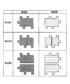
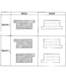
- 6 to 9 show in a table another example of the combination of the shape of the anode foil 10 used in the first step and the shape of the cathode foil 20 used in the second step.
- 6 and 7 are examples of configuring an electrolytic capacitor with 10 terminals (anode 5 terminal, cathode 5 terminal), and FIGS. 8 and 9 show electrolysis of 8 terminals (anode 4 terminal, cathode 4 terminal). This is an example of configuring a capacitor.
- Configuration example 1 shown in FIG. 6 corresponds to a combination of the anode foil of the capacitor element shown in FIG. 4 and the cathode foil shown in FIG.
- the anode foil and / or the cathode foil may be composed of a plurality of foil pieces, and the plurality of foil pieces may be arranged side by side.
- the direction of the current flowing through the anode foil and / or the cathode foil is limited, and ESL can be easily controlled. Further, since the anode foil and the cathode foil become smaller, the handling in manufacturing becomes easier.
- the projecting position of the second region A 2 is used by combining a plurality of different anode foil, and / or fourth region A 4
- a plurality of cathode foils having different protrusion positions may be used in combination to form an element laminate.
- a pair of anode foil protruding position of the second area A 2 are different can be used. Further, a pair of cathode foil protruding position of the fourth region A 4 are different may be used.
- One of the pair of the anode foil, a first direction e.g., normal to the direction of the first main surface of the exterior body
- the first direction opposite direction e.g., no second region a 2 projecting toward the normal direction
- the other of the pair of anode foils has a second region A 2 projecting in the direction opposite to the first direction and does not have a second region A 2 projecting in the first direction.
- the one of the pair of the cathode foil, and a fourth area A 4 projecting toward the first direction no fourth area A 4 projecting toward the direction opposite to the first direction.
- the other of the pair of cathode foil has a fourth region A 4 projecting toward the direction opposite to the first direction, no fourth area A 4 projecting toward the first direction.
- a capacitor element (first capacitor element) using one of the pair of anode foils shown in Configuration Example 3 and a capacitor element (second capacitor element) using the other of the pair of anode foils are alternately alternated.
- the electrolytic capacitor 100 having the cross-sectional structure shown in FIGS. 3A to 3C can be obtained.
- three or more types of anode foils may be used in combination, or three or more types of cathode foils may be used in combination.
- at least one of the plurality of anode foils or the plurality of cathode foils used in combination may be composed of a plurality of foil pieces.
- the fourth region A 4 of the second region A 2 and cathode foil of the anode foil a first direction (e.g., normal to the direction of the first main surface of the exterior body ) And / or the direction opposite to the first direction (for example, the normal direction of the third main surface of the exterior body).
- a first direction e.g., normal to the direction of the first main surface of the exterior body
- / or the direction opposite to the first direction for example, the normal direction of the third main surface of the exterior body.
- it does not have a second region A 2 and a fourth region A 4 projecting in a direction intersecting the first direction (eg, the normal direction of the second or fourth main surface of the exterior body).
- the anode foil and / or the cathode foil may be composed of a plurality of foil pieces, and the plurality of foil pieces may be arranged side by side. That is, the anode foil and / or the cathode foil may be divided in the second direction perpendicular to the first direction to form the foil pieces as in the configuration example 7, and in the first direction as in the configuration example 8.
- the foil pieces may be divided into pieces. Further, as in the configuration example 9, the anode foil and / or the cathode foil may be divided in the first direction and the second direction, and may be composed of four foil pieces.
- a plurality of anode foils having different protrusion positions of the second region A 2 are used in combination, and / or the protrusion position of the fourth region A 4 is used.
- the element laminate may be formed by using a plurality of cathode foils having different amounts of each other in combination.
- a pair of anode foil protruding position of the second area A 2 are different can be used. Further, a pair of cathode foil protruding position of the fourth region A 4 are different may be used.
- One of the pair of anode foils has a second region A 2 projecting in the first direction and does not have a second region A 2 projecting in the direction opposite to the first direction.
- the other of the pair of anode foils has a second region A 2 projecting in the direction opposite to the first direction and does not have a second region A 2 projecting in the first direction.
- the one of the pair of the cathode foil, and a fourth area A 4 projecting toward the first direction no fourth area A 4 projecting toward the direction opposite to the first direction.
- the other of the pair of cathode foil has a fourth region A 4 projecting toward the direction opposite to the first direction, no fourth area A 4 projecting toward the first direction.
- a capacitor element (first capacitor element) using one of the pair of anode foils shown in Configuration Example 10 and a capacitor element (second capacitor element) using the other of the pair of anode foils are alternately laminated.
- the element laminate may be formed and the electrolytic capacitor 100 may be manufactured.
- the anode foil and / or the cathode foil is composed of a plurality of strip-shaped foil pieces, and the positions of the strips of the plurality of strip-shaped foil pieces in the longitudinal direction are adjacent to each other in the stacking direction.
- the anode extraction portion and / or the cathode extraction portion may be formed to form an element laminate.
- At least one first external electrode and one second external electrode may be provided on the first main surface 31A, respectively.
- the distance between the first main surface 31A and the third main surface 31C is shorter than the distance between the second main surface 31B and the fourth main surface 31D.
- the distance between the first main surface 31A and the third main surface 31C may be longer than the distance between the second main surface 31B and the fourth main surface 31D. That is, when the electrolytic capacitor is viewed from above (for example, from the direction perpendicular to the main surface of the anode), the exterior in which at least one first external electrode and at least one second external electrode are substantially rectangular. It may be provided on the surface forming the short side of the contour line of the body. In this case, the distance between the first external electrode and the second external electrode becomes short, and ESL can be easily reduced.
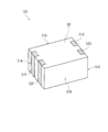
- FIG. 10 is a perspective view schematically showing the electrolytic capacitor 101 according to the present embodiment.
- the electrolytic capacitor 101 includes the above-mentioned element laminate, an exterior body 30 for sealing the element laminate, first external electrodes 51F and 51G, and second external electrodes 52F and 52G.
- the first external electrodes 51F and 51G are the anodes of the electrolytic capacitor 101
- the second external electrodes 52F and 52G are the cathodes of the electrolytic capacitor 101.
- the first external electrode 51F and the second external electrode 52F are provided on the first main surface 31A.
- the first external electrode 51G and the second external electrode 52G are provided on the third main surface 31C.
- the first main surface 31A and the third main surface 31C correspond to the short sides of the rectangular contour line when the electrolytic capacitor is viewed from above.
- the electrolytic capacitor 101 having 4 terminals (2 terminals for the anode and 2 terminals for the cathode) is configured.
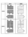
- FIG. 11 shows in a table an example of a combination of the shape of the anode foil 10 used in the first step for manufacturing the electrolytic capacitor 101 and the shape of the cathode foil 20 used in the second step.
- Configuration example 12 shown in FIG. 11 is an example in which one anode foil and one cathode foil are used.
- the projecting position of the second region A 2 is used by combining a plurality of different anode foil, and / or, the projecting position of the fourth region A 4 is a combination of a plurality of different cathode foils It may be used to form an element laminate.
- a first direction e.g., normal to the direction of the first main surface of the exterior body
- the first direction opposite direction e.g., no second region a 2 projecting toward the normal direction
- the other of the pair of anode foils has a second region A 2 projecting in the direction opposite to the first direction and does not have a second region A 2 projecting in the first direction. Further, the one of the pair of the cathode foil, and a fourth area A 4 projecting toward the first direction, no fourth area A 4 projecting toward the direction opposite to the first direction. The other of the pair of cathode foil has a fourth region A 4 projecting toward the direction opposite to the first direction, no fourth area A 4 projecting toward the first direction.
- the pair of anode foils shown in Configuration Example 13 and the cathode foils shown in Configuration Example 12 may be combined.
- the pair of cathode foils shown in Configuration Example 13 and the anode foils shown in Configuration Example 12 may be combined.
- the first external electrode 51F provided on the first main surface 31A faces the first external electrode 51G provided on the third main surface 31C and is provided on the first main surface 31A.
- the second external electrode 52F faces the second external electrode 52G provided on the third main surface 31C.
- the first external electrode 51F provided on the first main surface 31A may face the second external electrode 52G provided on the third main surface 31C.
- the second external electrode 52F provided on the first main surface 31A may face the first external electrode 51G provided on the third main surface 31C.
- FIG. 12 shows in a table another example of the combination of the shape of the anode foil 10 used in the first step and the shape of the cathode foil 20 used in the second step.
- FIG. 12 shows an example in which an electrolytic capacitor having four terminals (anode 2 terminal and cathode 2 terminal) is configured as in FIG.
- Configuration example 14 shown in FIG. 12 is an example in which one anode foil and one cathode foil are used.
- a plurality of anode foils having different protrusion positions of the second region A 2 are used in combination, and / or the protrusion position of the fourth region A 4 is set.
- This is an example of forming an element laminate by using a plurality of different cathode foils in combination. Since the pair of anode foils shown in Configuration Example 15 and the pair of cathode foils shown in Configuration Example 15 coincide with each other when rotated 180 degrees, this can be realized by producing a plurality of foil pieces having the same shape.
- the pair of anode foils shown in Configuration Example 15 and the cathode foils shown in Configuration Example 14 may be combined.
- the pair of cathode foils shown in Configuration Example 15 and the anode foils shown in Configuration Example 14 may be combined.
- the first external electrode 51F and the second external electrode 52F are main surfaces (second main surface) that continuously intersect the first main surface 31A from the first main surface 31A. It may extend to a part of the surface or the fourth main surface).
- the first external electrode 51G and the second external electrode 52G extend from the third main surface 31C to a part of the main surface (second main surface or fourth main surface) that continuously intersects the third main surface 31C. It may be present.
- the first external electrode is electrically connected to the end face of the anode foil on both the first or third main surface on the short side and the second or fourth main surface on the long side. Can be connected to.
- the second external electrode is electrically connected to the end face of the cathode foil on both the first or third main surface on the short side and the second or fourth main surface on the long side. obtain.
- the electrolytic capacitor of the present disclosure can be used in various applications requiring high capacity and low ESL.
- Electrolytic capacitors 10: Anode foil 1: End 3A: End face 4: Core 5: Porous 7: Solid electrolyte layer 8: Insulating film (resist) 20: Cathode foil 2: End 3B: End face 23: Adhesive layer 24: Substrate 30: Exterior body 31A: First main surface of exterior body 31B: Second main surface of exterior body 31C: Third main surface of exterior body 31D : Fourth main surface of the exterior body 40: Capacitor element 40A: First capacitor element 40B: Second capacitor element 51A to 51G: First external electrode 52A to 52G: Second external electrode 53: Contact layer 54: Intermediate electrode layers 100, 101, 102: Electrolytic capacitors
Landscapes
- Engineering & Computer Science (AREA)
- Power Engineering (AREA)
- Microelectronics & Electronic Packaging (AREA)
- Chemical & Material Sciences (AREA)
- Materials Engineering (AREA)
- Manufacturing & Machinery (AREA)
- Fixed Capacitors And Capacitor Manufacturing Machines (AREA)
Priority Applications (3)
| Application Number | Priority Date | Filing Date | Title |
|---|---|---|---|
| US17/905,637 US12374505B2 (en) | 2020-03-31 | 2021-03-18 | Electrolytic capacitor |
| CN202180023543.3A CN115335935A (zh) | 2020-03-31 | 2021-03-18 | 电解电容器 |
| JP2022511874A JPWO2021200197A1 (https=) | 2020-03-31 | 2021-03-18 |
Applications Claiming Priority (4)
| Application Number | Priority Date | Filing Date | Title |
|---|---|---|---|
| JP2020-064791 | 2020-03-31 | ||
| JP2020064791 | 2020-03-31 | ||
| JP2020-183105 | 2020-10-30 | ||
| JP2020183105 | 2020-10-30 |
Publications (1)
| Publication Number | Publication Date |
|---|---|
| WO2021200197A1 true WO2021200197A1 (ja) | 2021-10-07 |
Family
ID=77928684
Family Applications (1)
| Application Number | Title | Priority Date | Filing Date |
|---|---|---|---|
| PCT/JP2021/011000 Ceased WO2021200197A1 (ja) | 2020-03-31 | 2021-03-18 | 電解コンデンサ |
Country Status (4)
| Country | Link |
|---|---|
| US (1) | US12374505B2 (https=) |
| JP (1) | JPWO2021200197A1 (https=) |
| CN (1) | CN115335935A (https=) |
| WO (1) | WO2021200197A1 (https=) |
Cited By (2)
| Publication number | Priority date | Publication date | Assignee | Title |
|---|---|---|---|---|
| WO2023176684A1 (ja) * | 2022-03-15 | 2023-09-21 | パナソニックIpマネジメント株式会社 | キャパシタ及び電源モジュール |
| WO2026058571A1 (ja) * | 2024-09-11 | 2026-03-19 | 株式会社村田製作所 | 固体電解コンデンサおよび固体電解コンデンサの製造方法 |
Citations (5)
| Publication number | Priority date | Publication date | Assignee | Title |
|---|---|---|---|---|
| JPH11288846A (ja) * | 1998-02-09 | 1999-10-19 | Matsushita Electric Ind Co Ltd | 4端子コンデンサ |
| JP2003178933A (ja) * | 2001-10-05 | 2003-06-27 | Matsushita Electric Ind Co Ltd | コンデンサ |
| WO2003107366A1 (ja) * | 2002-06-18 | 2003-12-24 | ティーディーケイ株式会社 | 固体電解コンデンサおよびその製造方法 |
| JP2006203168A (ja) * | 2004-12-24 | 2006-08-03 | Murata Mfg Co Ltd | 積層コンデンサおよびその実装構造 |
| JP2009123938A (ja) * | 2007-11-15 | 2009-06-04 | Panasonic Corp | チップ形固体電解コンデンサ |
Family Cites Families (26)
| Publication number | Priority date | Publication date | Assignee | Title |
|---|---|---|---|---|
| JPS5830121A (ja) * | 1981-08-14 | 1983-02-22 | 日本電気株式会社 | 有極性チツプ型電子部品 |
| JPH04367212A (ja) * | 1991-06-14 | 1992-12-18 | Nec Corp | チップ型固体電解コンデンサの製造方法 |
| JP3199871B2 (ja) * | 1992-09-30 | 2001-08-20 | ニチコン株式会社 | チップ型固体電解コンデンサ |
| JPH07226342A (ja) * | 1994-02-09 | 1995-08-22 | Matsushita Electric Ind Co Ltd | チップ状固体電解コンデンサ |
| US5880925A (en) * | 1997-06-27 | 1999-03-09 | Avx Corporation | Surface mount multilayer capacitor |
| US6292350B1 (en) * | 1997-11-10 | 2001-09-18 | Murata Manufacturing, Co., Ltd | Multilayer capacitor |
| US6185091B1 (en) | 1998-02-09 | 2001-02-06 | Matsushita Electric Industrial Co., Ltd. | Four-terminal capacitor |
| US6590762B2 (en) * | 2001-08-06 | 2003-07-08 | Intel Corporation | Layered polymer on aluminum stacked capacitor |
| US6661644B2 (en) | 2001-10-05 | 2003-12-09 | Matsushita Electric Industrial Co., Ltd. | Capacitor |
| JP2003289018A (ja) * | 2002-03-28 | 2003-10-10 | Tdk Corp | チップ型積層コンデンサ |
| JP2004095816A (ja) * | 2002-08-30 | 2004-03-25 | Matsushita Electric Ind Co Ltd | チップ形コンデンサ |
| US7046500B2 (en) * | 2004-07-20 | 2006-05-16 | Samsung Electro-Mechanics Co., Ltd. | Laminated ceramic capacitor |
| WO2006067939A1 (ja) | 2004-12-24 | 2006-06-29 | Murata Manufacturing Co., Ltd. | 積層コンデンサおよびその実装構造 |
| JP2008021773A (ja) * | 2006-07-12 | 2008-01-31 | Matsushita Electric Ind Co Ltd | チップ形固体電解コンデンサ |
| TW200828371A (en) | 2006-09-21 | 2008-07-01 | Matsushita Electric Industrial Co Ltd | Chip-type filter |
| JP5040230B2 (ja) | 2006-09-21 | 2012-10-03 | パナソニック株式会社 | チップ形固体電解コンデンサ |
| JP2009010068A (ja) * | 2007-06-27 | 2009-01-15 | Panasonic Corp | チップ形固体電解コンデンサ |
| KR100925603B1 (ko) * | 2007-09-28 | 2009-11-06 | 삼성전기주식회사 | 적층형 캐패시터 |
| US8421557B2 (en) | 2007-11-15 | 2013-04-16 | Panasonic Corporation | Chip-type solid electrolytic capacitor and chip-type filter |
| JP5073011B2 (ja) * | 2010-06-10 | 2012-11-14 | 佐賀三洋工業株式会社 | 固体電解コンデンサ及びその製造方法 |
| JP6024483B2 (ja) * | 2013-01-29 | 2016-11-16 | 株式会社村田製作所 | 積層型セラミック電子部品 |
| KR20150031759A (ko) * | 2013-09-16 | 2015-03-25 | 삼성전기주식회사 | 고체 전해 캐패시터 |
| KR101548865B1 (ko) * | 2014-05-07 | 2015-08-31 | 삼성전기주식회사 | 탄탈륨 캐패시터 |
| KR102281461B1 (ko) * | 2015-08-07 | 2021-07-27 | 삼성전기주식회사 | 고체 전해커패시터 및 그 실장 기판 |
| CN109791844B (zh) * | 2016-10-17 | 2021-10-26 | 株式会社村田制作所 | 固体电解电容器 |
| JP2025030121A (ja) * | 2023-08-23 | 2025-03-07 | 株式会社三共 | 遊技機 |
-
2021
- 2021-03-18 WO PCT/JP2021/011000 patent/WO2021200197A1/ja not_active Ceased
- 2021-03-18 JP JP2022511874A patent/JPWO2021200197A1/ja active Pending
- 2021-03-18 US US17/905,637 patent/US12374505B2/en active Active
- 2021-03-18 CN CN202180023543.3A patent/CN115335935A/zh active Pending
Patent Citations (5)
| Publication number | Priority date | Publication date | Assignee | Title |
|---|---|---|---|---|
| JPH11288846A (ja) * | 1998-02-09 | 1999-10-19 | Matsushita Electric Ind Co Ltd | 4端子コンデンサ |
| JP2003178933A (ja) * | 2001-10-05 | 2003-06-27 | Matsushita Electric Ind Co Ltd | コンデンサ |
| WO2003107366A1 (ja) * | 2002-06-18 | 2003-12-24 | ティーディーケイ株式会社 | 固体電解コンデンサおよびその製造方法 |
| JP2006203168A (ja) * | 2004-12-24 | 2006-08-03 | Murata Mfg Co Ltd | 積層コンデンサおよびその実装構造 |
| JP2009123938A (ja) * | 2007-11-15 | 2009-06-04 | Panasonic Corp | チップ形固体電解コンデンサ |
Cited By (2)
| Publication number | Priority date | Publication date | Assignee | Title |
|---|---|---|---|---|
| WO2023176684A1 (ja) * | 2022-03-15 | 2023-09-21 | パナソニックIpマネジメント株式会社 | キャパシタ及び電源モジュール |
| WO2026058571A1 (ja) * | 2024-09-11 | 2026-03-19 | 株式会社村田製作所 | 固体電解コンデンサおよび固体電解コンデンサの製造方法 |
Also Published As
| Publication number | Publication date |
|---|---|
| US12374505B2 (en) | 2025-07-29 |
| CN115335935A (zh) | 2022-11-11 |
| US20230119189A1 (en) | 2023-04-20 |
| JPWO2021200197A1 (https=) | 2021-10-07 |
Similar Documents
| Publication | Publication Date | Title |
|---|---|---|
| US12293881B2 (en) | Electrolytic capacitor and method for producing same | |
| CN1741213B (zh) | 固体电解电容器 | |
| JP5131079B2 (ja) | 固体電解コンデンサの製造方法 | |
| US20100008017A1 (en) | Laminated ceramic electronic component | |
| US12456586B2 (en) | Electrolytic capacitor | |
| US12293877B2 (en) | Electrolytic capacitor | |
| US11972907B2 (en) | Solid electrolytic capacitor | |
| JP2010062406A (ja) | 固体電解コンデンサ及びその製造方法 | |
| WO2022163644A1 (ja) | 電解コンデンサ | |
| WO2021200197A1 (ja) | 電解コンデンサ | |
| US12057274B2 (en) | Packaging structures for electronic elements and solid electrolytic capacitor elements and methods thereof | |
| CN217214477U (zh) | 电子组件封装结构及半成品组合体 | |
| CN113327771A (zh) | 一种片式导电聚合物电容器封装方法及电容器 | |
| JPH0684716A (ja) | 固体電解コンデンサの製造方法 | |
| WO2021230089A1 (ja) | 集積回路の電源供給用の電気回路、コンデンサ及び集積回路付電気回路 | |
| JP4599653B2 (ja) | シートコンデンサ | |
| CN114746968A (zh) | 固体电解电容器 | |
| JP4831240B2 (ja) | シートコンデンサの製造方法 | |
| JP7736171B2 (ja) | 電解コンデンサ | |
| WO2022181606A1 (ja) | フィルタ回路 | |
| WO2021038900A1 (ja) | 電解コンデンサ | |
| WO2021038901A1 (ja) | 電解コンデンサ、及び、電解コンデンサの製造方法 | |
| JP2023028537A (ja) | 電気装置、フィルタ装置及びコンデンサモジュール |
Legal Events
| Date | Code | Title | Description |
|---|---|---|---|
| 121 | Ep: the epo has been informed by wipo that ep was designated in this application |
Ref document number: 21781959 Country of ref document: EP Kind code of ref document: A1 |
|
| ENP | Entry into the national phase |
Ref document number: 2022511874 Country of ref document: JP Kind code of ref document: A |
|
| NENP | Non-entry into the national phase |
Ref country code: DE |
|
| 122 | Ep: pct application non-entry in european phase |
Ref document number: 21781959 Country of ref document: EP Kind code of ref document: A1 |
|
| WWG | Wipo information: grant in national office |
Ref document number: 17905637 Country of ref document: US |