WO2021161684A1 - 撮像ユニット及び測定装置 - Google Patents
撮像ユニット及び測定装置 Download PDFInfo
- Publication number
- WO2021161684A1 WO2021161684A1 PCT/JP2021/000041 JP2021000041W WO2021161684A1 WO 2021161684 A1 WO2021161684 A1 WO 2021161684A1 JP 2021000041 W JP2021000041 W JP 2021000041W WO 2021161684 A1 WO2021161684 A1 WO 2021161684A1
- Authority
- WO
- WIPO (PCT)
- Prior art keywords
- wavelength
- light
- imaging
- dichroic mirror
- transmittance
- Prior art date
Links
Images


Classifications
-
- G—PHYSICS
- G01—MEASURING; TESTING
- G01B—MEASURING LENGTH, THICKNESS OR SIMILAR LINEAR DIMENSIONS; MEASURING ANGLES; MEASURING AREAS; MEASURING IRREGULARITIES OF SURFACES OR CONTOURS
- G01B11/00—Measuring arrangements characterised by the use of optical techniques
- G01B11/02—Measuring arrangements characterised by the use of optical techniques for measuring length, width or thickness
- G01B11/06—Measuring arrangements characterised by the use of optical techniques for measuring length, width or thickness for measuring thickness ; e.g. of sheet material
- G01B11/0616—Measuring arrangements characterised by the use of optical techniques for measuring length, width or thickness for measuring thickness ; e.g. of sheet material of coating
- G01B11/0625—Measuring arrangements characterised by the use of optical techniques for measuring length, width or thickness for measuring thickness ; e.g. of sheet material of coating with measurement of absorption or reflection
- G01B11/0633—Measuring arrangements characterised by the use of optical techniques for measuring length, width or thickness for measuring thickness ; e.g. of sheet material of coating with measurement of absorption or reflection using one or more discrete wavelengths
-
- G—PHYSICS
- G01—MEASURING; TESTING
- G01B—MEASURING LENGTH, THICKNESS OR SIMILAR LINEAR DIMENSIONS; MEASURING ANGLES; MEASURING AREAS; MEASURING IRREGULARITIES OF SURFACES OR CONTOURS
- G01B11/00—Measuring arrangements characterised by the use of optical techniques
- G01B11/02—Measuring arrangements characterised by the use of optical techniques for measuring length, width or thickness
- G01B11/06—Measuring arrangements characterised by the use of optical techniques for measuring length, width or thickness for measuring thickness ; e.g. of sheet material
- G01B11/0608—Height gauges
-
- G—PHYSICS
- G01—MEASURING; TESTING
- G01B—MEASURING LENGTH, THICKNESS OR SIMILAR LINEAR DIMENSIONS; MEASURING ANGLES; MEASURING AREAS; MEASURING IRREGULARITIES OF SURFACES OR CONTOURS
- G01B11/00—Measuring arrangements characterised by the use of optical techniques
- G01B11/02—Measuring arrangements characterised by the use of optical techniques for measuring length, width or thickness
- G01B11/06—Measuring arrangements characterised by the use of optical techniques for measuring length, width or thickness for measuring thickness ; e.g. of sheet material
- G01B11/0616—Measuring arrangements characterised by the use of optical techniques for measuring length, width or thickness for measuring thickness ; e.g. of sheet material of coating
- G01B11/0625—Measuring arrangements characterised by the use of optical techniques for measuring length, width or thickness for measuring thickness ; e.g. of sheet material of coating with measurement of absorption or reflection
-
- G—PHYSICS
- G01—MEASURING; TESTING
- G01B—MEASURING LENGTH, THICKNESS OR SIMILAR LINEAR DIMENSIONS; MEASURING ANGLES; MEASURING AREAS; MEASURING IRREGULARITIES OF SURFACES OR CONTOURS
- G01B11/00—Measuring arrangements characterised by the use of optical techniques
- G01B11/02—Measuring arrangements characterised by the use of optical techniques for measuring length, width or thickness
- G01B11/06—Measuring arrangements characterised by the use of optical techniques for measuring length, width or thickness for measuring thickness ; e.g. of sheet material
- G01B11/0691—Measuring arrangements characterised by the use of optical techniques for measuring length, width or thickness for measuring thickness ; e.g. of sheet material of objects while moving
-
- G—PHYSICS
- G01—MEASURING; TESTING
- G01B—MEASURING LENGTH, THICKNESS OR SIMILAR LINEAR DIMENSIONS; MEASURING ANGLES; MEASURING AREAS; MEASURING IRREGULARITIES OF SURFACES OR CONTOURS
- G01B15/00—Measuring arrangements characterised by the use of electromagnetic waves or particle radiation, e.g. by the use of microwaves, X-rays, gamma rays or electrons
- G01B15/02—Measuring arrangements characterised by the use of electromagnetic waves or particle radiation, e.g. by the use of microwaves, X-rays, gamma rays or electrons for measuring thickness
-
- G—PHYSICS
- G01—MEASURING; TESTING
- G01J—MEASUREMENT OF INTENSITY, VELOCITY, SPECTRAL CONTENT, POLARISATION, PHASE OR PULSE CHARACTERISTICS OF INFRARED, VISIBLE OR ULTRAVIOLET LIGHT; COLORIMETRY; RADIATION PYROMETRY
- G01J3/00—Spectrometry; Spectrophotometry; Monochromators; Measuring colours
- G01J3/02—Details
- G01J3/0205—Optical elements not provided otherwise, e.g. optical manifolds, diffusers, windows
-
- G—PHYSICS
- G01—MEASURING; TESTING
- G01J—MEASUREMENT OF INTENSITY, VELOCITY, SPECTRAL CONTENT, POLARISATION, PHASE OR PULSE CHARACTERISTICS OF INFRARED, VISIBLE OR ULTRAVIOLET LIGHT; COLORIMETRY; RADIATION PYROMETRY
- G01J3/00—Spectrometry; Spectrophotometry; Monochromators; Measuring colours
- G01J3/02—Details
- G01J3/027—Control of working procedures of a spectrometer; Failure detection; Bandwidth calculation
-
- G—PHYSICS
- G01—MEASURING; TESTING
- G01J—MEASUREMENT OF INTENSITY, VELOCITY, SPECTRAL CONTENT, POLARISATION, PHASE OR PULSE CHARACTERISTICS OF INFRARED, VISIBLE OR ULTRAVIOLET LIGHT; COLORIMETRY; RADIATION PYROMETRY
- G01J3/00—Spectrometry; Spectrophotometry; Monochromators; Measuring colours
- G01J3/12—Generating the spectrum; Monochromators
-
- G—PHYSICS
- G01—MEASURING; TESTING
- G01J—MEASUREMENT OF INTENSITY, VELOCITY, SPECTRAL CONTENT, POLARISATION, PHASE OR PULSE CHARACTERISTICS OF INFRARED, VISIBLE OR ULTRAVIOLET LIGHT; COLORIMETRY; RADIATION PYROMETRY
- G01J3/00—Spectrometry; Spectrophotometry; Monochromators; Measuring colours
- G01J3/28—Investigating the spectrum
- G01J3/30—Measuring the intensity of spectral lines directly on the spectrum itself
- G01J3/36—Investigating two or more bands of a spectrum by separate detectors
-
- G—PHYSICS
- G01—MEASURING; TESTING
- G01J—MEASUREMENT OF INTENSITY, VELOCITY, SPECTRAL CONTENT, POLARISATION, PHASE OR PULSE CHARACTERISTICS OF INFRARED, VISIBLE OR ULTRAVIOLET LIGHT; COLORIMETRY; RADIATION PYROMETRY
- G01J9/00—Measuring optical phase difference; Determining degree of coherence; Measuring optical wavelength
-
- G—PHYSICS
- G01—MEASURING; TESTING
- G01N—INVESTIGATING OR ANALYSING MATERIALS BY DETERMINING THEIR CHEMICAL OR PHYSICAL PROPERTIES
- G01N21/00—Investigating or analysing materials by the use of optical means, i.e. using sub-millimetre waves, infrared, visible or ultraviolet light
- G01N21/84—Systems specially adapted for particular applications
- G01N21/8422—Investigating thin films, e.g. matrix isolation method
-
- G—PHYSICS
- G02—OPTICS
- G02B—OPTICAL ELEMENTS, SYSTEMS OR APPARATUS
- G02B27/00—Optical systems or apparatus not provided for by any of the groups G02B1/00 - G02B26/00, G02B30/00
- G02B27/10—Beam splitting or combining systems
- G02B27/14—Beam splitting or combining systems operating by reflection only
- G02B27/141—Beam splitting or combining systems operating by reflection only using dichroic mirrors
-
- G—PHYSICS
- G01—MEASURING; TESTING
- G01N—INVESTIGATING OR ANALYSING MATERIALS BY DETERMINING THEIR CHEMICAL OR PHYSICAL PROPERTIES
- G01N21/00—Investigating or analysing materials by the use of optical means, i.e. using sub-millimetre waves, infrared, visible or ultraviolet light
- G01N21/84—Systems specially adapted for particular applications
- G01N21/88—Investigating the presence of flaws or contamination
- G01N21/95—Investigating the presence of flaws or contamination characterised by the material or shape of the object to be examined
- G01N21/9501—Semiconductor wafers
Definitions
- the second emission spectrum g ( ⁇ ) (wavelength X3 in FIG. 3).
- the emission spectrum g ( ⁇ ) the spectrum is completely included between ⁇ 1 and ⁇ 2.
- the difference between the standardized difference between the transmitted light and the reflected light is calculated.
- f (lambda) of the transmitted light T f, the reflected light R f, the total amount of A f, the difference of the transmitted light and the reflected light is D f.
- g ( ⁇ ) of the transmitted light T g, the reflected light R g, a total light quantity A g, the difference of the transmitted light and the reflected light is D g.
- the center of gravity of the emission spectrum can be calculated from the design value of the filter, the amount of transmitted light, and the amount of reflected light. Based on the above principle, the center of gravity of the wavelength of the light incident on each pixel can be obtained with high accuracy.
- the control device 80 determines the quality of the sample by analyzing the processing result including the corrected image.
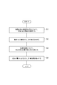
- FIG. 6 is a flowchart of the correction method.
- the correction unit 100 is installed upstream (previous stage) of the camera system 2.
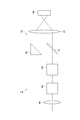
- the measuring device 1 separates the light from the sample by transmitting or reflecting it according to the wavelength, and the edge transition which is the width of the wavelength band in which the transmittance and the reflectance change according to the change of the wavelength.
- the tilted dichroic mirror 11 having a predetermined width, the fully reflective mirror 12 that reflects one of the light transmitted or reflected by the tilted dicroic mirror 11, and the other of the light transmitted or reflected by the tilted dicroic mirror 11 are the first.
- An imaging element 14 that captures images in one imaging region and images the light reflected by the total reflection mirror 12 in a second imaging region different from the first imaging region, and the transmittance and transmittance for wavelengths in the tilted dichroic mirror 11.
- a control device 80 for correcting images captured in a first imaging region and a second imaging region based on optical characteristics related to a change in transmittance is provided.
- an inclined dichroic mirror 11 having an edge transition width having a predetermined width is used, and the captured image is corrected based on the optical characteristics related to the change in the transmittance and the reflectance with respect to the wavelength in the inclined dichroic mirror 11.
- an inclined dichroic mirror 11 having an edge transition width having a predetermined width is used, light having a narrow wavelength width can be appropriately separated, but the optical characteristics change depending on, for example, the incident angle of the light with respect to the inclined dichroic mirror 11. As a result, it may not be possible to accurately derive the wavelength of light and acquire an appropriate image.
- the control device 80 stores in advance correction data in consideration of optical characteristics related to changes in transmittance and reflectance with respect to the wavelength of the tilted dichroic mirror 11, and uses the correction data to store a first imaging region and a second imaging region.
- the image captured in the imaging region may be corrected. According to such a configuration, the captured image can be easily and appropriately corrected based on the correction data stored in advance.
- the control device 80 may correct color spots caused by the angle of incidence of light on the tilted dichroic mirror 11.
- a separation optical element having an edge transition width is used, the optical characteristics of the tilted dichroic mirror 11 change according to the angle of incidence on the tilted dichroic mirror 11, and there is a problem that color spots occur in the captured image. .. In this respect, by correcting the color spots, an appropriate image with the color spots reduced can be obtained.
- the control device 80 may correct the deviation of the detection wavelength due to the boundary between the wavelength band in which the transmittance and the reflectance change according to the change in wavelength and the wavelength band in which the reflectance does not change.
- a boundary has optical characteristics different from those of a wavelength band in which the transmittance and the like change according to a change in wavelength. Therefore, if the wavelength is derived by the same calculation formula as the wavelength band in which the transmittance and the like change according to the change in the wavelength, the derivation result may be different from the original wavelength.
- the wavelength of light can be accurately derived and an appropriate image can be acquired.
- the image pickup element 14 may be a single image pickup element having a first image pickup region and a second image pickup region. As a result, a plurality of captured images can be obtained by a simple configuration using a single image sensor.
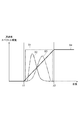
- the tilted dichroic mirror provided in front of the area sensor which is an image sensor, has a wavelength band (edge transition width) in which the light transmittance (and reflectance) changes according to a change in wavelength. It corresponds to all three colors of RGB, for example, 400 to 900 nm.
- FIG. 7 is a diagram for explaining the characteristics of the inclined dichroic mirror according to the modified example.
- the horizontal axis shows the wavelength
- the vertical axis shows the transmittance (in the case of a tilted dichroic mirror) and the spectral intensity (in the case of a light spectrum).
- the light transmittance (and reflectance) gradually changes according to the change in wavelength, and wavelengths other than the specific wavelength band.
- the band that is, the wavelength side lower than 400 nm and the wavelength side higher than 900 nm
- the light transmittance (and reflectance) is constant regardless of the change in wavelength.
- FIG. 7 shows that is, the wavelength side lower than 400 nm and the wavelength side higher than 900 nm.
- the wavelength band (edge transition width) in which the light transmission (and reflectance) changes according to the change in wavelength is the wavelength of light including a red wavelength component.
- the band (wavelength band shown on the right side in FIG. 7), the wavelength band of light containing a green wavelength component (wavelength band shown in the center in FIG. 7), and the wavelength band of light containing a blue wavelength component (FIG. 7). Includes all of the wavelength bands shown on the left side).
- FIG. 8 is a diagram schematically showing the camera system 90A according to the modified example.
- the finite focus lens 92A is a lens that collects light (emission) from the sample 150 (object) to be observed.
- the distance from the finite focus lens 92A to the area sensor 94 and the distance from the finite focus lens 92A to the area sensor 95 are set to predetermined values.
- the light that has passed through the finite focus lens 92A is incident on the tilted dichroic mirror 91.
- the bandpass filter 93 is provided, for example, in the front stage (upstream) of the finite focus lens 92A, and is a filter that removes light outside a predetermined wavelength range.
- the bandpass filter 93 removes light having a wavelength outside the range of 400 to 900 nm, for example.
- a plurality of bandpass filters 93 may be provided.
- the bandpass filter 93 may be provided in the region shown by the broken line in FIG. 8, that is, in the rear stage (downstream) of the finite focus lens 92A and the front stage (upstream) of the tilted dichroic mirror 91, or the area sensor 94, It may be provided in the region of the front stage (upstream) of the 95 and the rear stage (downstream) of the inclined dichroic mirror 91.
- the two bandpass filters 93 and 93 have the same characteristics.
- the camera system 90A may be provided with a plurality of bandpass filters 93 configured to be switchable according to the light from the sample 150.
- the plurality of bandpass filters 93 in this case have different wavelength bands for filtering from each other (details will be described later).
- the inclined dichroic mirror 91 is a mirror created by using a special optical material, and separates light from a sample 150 by transmitting and reflecting it according to a wavelength, and has a transmittance and a reflectance in a predetermined wavelength width. It is a changing mirror.
- the wavelength band (edge transition width) in which the light transmission (and reflectance) changes according to the change in wavelength is the wavelength of light including a red wavelength component. It includes all of the band, the wavelength band of light including the wavelength component of green, and the wavelength band of light including the wavelength component of blue.
- the correction process will be explained.
- the tilted dichroic mirror 91 and the bandpass filter 93 when light is incident obliquely (when it is not at the pupil position of the objective lens), the light incident on each pixel is transmitted through a part of the light instead of the whole, and the tilted dichroic filter 93 is tilted.
- the transmission wavelength may shift due to the unevenness of the in-plane uniformity of the mirror 91 and the bandpass filter 93.
- the wavelength characteristic is distorted from a straight line, there is an effect of smoothing the wavelength characteristic.
- the camera system 90A may be configured to include one type of bandpass filter 93 (one type of range of wavelength bands to be filtered) and area sensors 94 and 95 which are monochrome sensors.
- the bandpass filter 93 removes light having a wavelength outside the range of, for example, 400 to 900 nm.
- the light incident on the area sensors 94 and 95 may be mixed with three RGB colors.
- the control device (not shown) obtains the averaged wavelength center of gravity of the light in the wavelength band transmitted through the bandpass filter 93 (light in which three RGB colors are mixed).
- the control device sets the wavelength center of gravity for each wavelength band. It can be obtained with high accuracy. Specifically, the wavelength center of gravity of the color of each pixel of a TV, a display, or the like can be obtained with high accuracy in nm units according to this embodiment.
- the camera system 90A may be configured to include a plurality of types of bandpass filters 93 having different wavelength bands for filtering each other, and area sensors 94 and 95 which are monochrome sensors.
- the plurality of types of bandpass filters 93 in this case are provided so as to be able to be taken in and out (switched) according to the light emission from the sample 150.
- a control device (not shown) is used by switching between a plurality of types of bandpass filters 93. Can obtain the wavelength center of gravity of light only in a specific wavelength band (wavelength band corresponding to each bandpass filter 93).
- the control device has a wavelength center of gravity of only the red wavelength component when the bandpass filter 93 for removing light having a wavelength other than the wavelength band of the red wavelength component (for example, 700 to 900 nm) is set.
- a bandpass filter 93 for removing light having a wavelength other than the wavelength band of the green wavelength component for example, 550 to 700 nm
- the wavelength center of gravity of only the green wavelength component is obtained, and the blue wavelength component is obtained.
- the bandpass filter 93 for removing light having a wavelength other than the wavelength band for example, 400 to 550 nm
- the wavelength center of gravity of only the blue wavelength component is obtained.
- the wavelength center of gravity can be appropriately obtained (that is, an appropriate inspection can be performed) for a color expressed by superimposing a plurality of wavelengths.
- the colors of printing and light emission are made by superimposing three RGB colors according to the human eye.
- the wavelength center of gravity of each of the colors superimposed in this way the mixed color can be inspected with high accuracy.
- a hyperspectral camera as the imaging unit, the center of gravity of more wavelengths may be inspected at the same time.
- a hyperspectral camera is composed of, for example, a spectroscope and an imaging unit.
- FIG. 9 is a diagram schematically showing a camera system 90B according to another modified example.
- the differences from the configuration shown in FIG. 8 will be mainly described.
- the camera system 90B includes an inclined dichroic mirror 91 (separation optical element), an infinity focus lens (infinity correction lens) 92B, a bandpass filter 93, and an area sensor 94 (second imaging).
- a unit an area sensor 95 (first imaging unit), and imaging lenses 96 and 97.
- the tilted dichroic mirror 91 and the area sensors 94 and 95 are similar to these configurations in the camera system 90A described above.
- the infinite focus lens 92B is a collimator lens that converts light (emission) from sample 150 (object) to be observed into parallel light.
- the infinite focus lens 92B is aberration-corrected so that parallel light can be obtained.
- the parallel light output from the infinite focus lens 92B is incident on the inclined dichroic mirror 91.
- the imaging lens 96 is a lens that forms an image of the light transmitted through the inclined dichroic mirror 91 on the area sensor 94.
- the imaging lens 97 is a lens that forms an image of the light transmitted through the inclined dichroic mirror 91 on the area sensor 95.
- the bandpass filter 93 is provided, for example, in the rear stage (downstream) of the infinite focus lens 92B and in the front stage (upstream) of the tilted dichroic mirror 91, and is a filter that removes light outside a predetermined wavelength range.
- the bandpass filter 93 removes light having a wavelength outside the range of 400 to 900 nm, for example.
- a plurality of bandpass filters 93 may be provided.
- the bandpass filter 93 may be provided in the region shown by the broken line in FIG. 9, that is, the region in the front stage (upstream) of the infinite focus lens 92B, or in the front stage (upstream) and the imaging lens of the area sensors 94 and 95.
- the bandpass filters 93 provided in front of the area sensors 94 and 95 have the same characteristics, and the bandpass filters 93 provided in front of the imaging lenses 96 and 97 have the same characteristics.
- the above-mentioned three embodiments can be considered as in the case of the camera system 90A.
- the camera system separates the light from the object by transmitting and reflecting it according to the wavelength, and the transmittance and the reflectance change in a predetermined wavelength width. It includes a separation optical element, a first imaging unit that captures the light transmitted by the separation optical element, and a second imaging unit that captures the light reflected by the separation optical element.
- the separation optical element whose transmittance and reflectance change according to the wavelength, it is possible to appropriately separate light having a narrow wavelength width, and appropriately according to the imaging result in the imaging unit.
- the wavelength center of gravity can be obtained.
- the light passing through the separation optical element can be directly received by the image pickup unit (first image pickup unit and second image pickup unit), so that the camera system can be configured. It is possible to realize miniaturization.
- the wavelength range in which the first imaging unit and the second imaging unit have sensitivity corresponds to the wavelength range in which the transmittance and the reflectance change in the separation optical element. .. According to such a configuration, the change (difference) in wavelength can be appropriately acquired from the imaging result in the imaging unit, and the center of gravity of the wavelength can be appropriately obtained.
- the camera system according to the modified example is equipped with a plurality of types of bandpass filters configured to be switchable according to the light from the object.
- a plurality of types of bandpass filters are switched and used, so that the control device (not shown) has a specific wavelength. It is possible to obtain the wavelength center of gravity of light only in the band (wavelength band corresponding to each bandpass filter). That is, the control device (not shown) obtains the wavelength center of gravity of only the red wavelength component when a bandpass filter for removing light having a wavelength other than the wavelength band of the red wavelength component is set, and the green wavelength component.
- the wavelength center of gravity of only the blue wavelength component can be obtained.
- Imaging element imaging unit
- 11,21,31 ... Inclined dichroic mirror separation optical element
- 12,22,32 ... Total reflection mirror reflection optical element
- 14,24,34 ... Imaging element (imaging unit)
- 80 Control device (processing unit, analysis unit).
Landscapes
- Physics & Mathematics (AREA)
- General Physics & Mathematics (AREA)
- Spectroscopy & Molecular Physics (AREA)
- Immunology (AREA)
- Biochemistry (AREA)
- Pathology (AREA)
- Health & Medical Sciences (AREA)
- Life Sciences & Earth Sciences (AREA)
- Chemical & Material Sciences (AREA)
- Analytical Chemistry (AREA)
- General Health & Medical Sciences (AREA)
- Mathematical Physics (AREA)
- Optics & Photonics (AREA)
- Electromagnetism (AREA)
- Length Measuring Devices By Optical Means (AREA)
- Investigating Or Analysing Materials By Optical Means (AREA)
- Spectrometry And Color Measurement (AREA)
- Optical Filters (AREA)
- Testing Or Measuring Of Semiconductors Or The Like (AREA)
Priority Applications (9)
| Application Number | Priority Date | Filing Date | Title |
|---|---|---|---|
| CN202180013797.7A CN115087849A (zh) | 2020-02-13 | 2021-01-04 | 摄像单元及测定装置 |
| US17/797,206 US20230061667A1 (en) | 2020-02-13 | 2021-01-04 | Imaging unit and measurement device |
| EP24195594.7A EP4443120A3 (en) | 2020-02-13 | 2021-01-04 | Imaging unit and measurement device |
| KR1020227024143A KR20220137629A (ko) | 2020-02-13 | 2021-01-04 | 촬상 유닛 및 측정 장치 |
| EP21754639.9A EP4086597B1 (en) | 2020-02-13 | 2021-01-04 | Imaging unit and measurement device |
| JP2022500259A JP7629437B2 (ja) | 2020-02-13 | 2021-01-04 | 撮像ユニット及び測定装置 |
| JP2023135422A JP7584594B2 (ja) | 2020-02-13 | 2023-08-23 | コンピュータ、プログラム、及び方法 |
| JP2024193128A JP2025013472A (ja) | 2020-02-13 | 2024-11-01 | コンピュータ、プログラム、及び方法 |
| JP2025015191A JP2025087682A (ja) | 2020-02-13 | 2025-01-31 | 撮像ユニット及び測定装置 |
Applications Claiming Priority (2)
| Application Number | Priority Date | Filing Date | Title |
|---|---|---|---|
| JP2020022724 | 2020-02-13 | ||
| JP2020-022724 | 2020-02-13 |
Publications (1)
| Publication Number | Publication Date |
|---|---|
| WO2021161684A1 true WO2021161684A1 (ja) | 2021-08-19 |
Family
ID=77291527
Family Applications (3)
| Application Number | Title | Priority Date | Filing Date |
|---|---|---|---|
| PCT/JP2021/000041 WO2021161684A1 (ja) | 2020-02-13 | 2021-01-04 | 撮像ユニット及び測定装置 |
| PCT/JP2021/003768 WO2021161854A1 (ja) | 2020-02-13 | 2021-02-02 | 高さ計測装置及び高さ計測方法 |
| PCT/JP2021/004743 WO2021161986A1 (ja) | 2020-02-13 | 2021-02-09 | 膜厚測定装置及び膜厚測定方法 |
Family Applications After (2)
| Application Number | Title | Priority Date | Filing Date |
|---|---|---|---|
| PCT/JP2021/003768 WO2021161854A1 (ja) | 2020-02-13 | 2021-02-02 | 高さ計測装置及び高さ計測方法 |
| PCT/JP2021/004743 WO2021161986A1 (ja) | 2020-02-13 | 2021-02-09 | 膜厚測定装置及び膜厚測定方法 |
Country Status (7)
Cited By (1)
| Publication number | Priority date | Publication date | Assignee | Title |
|---|---|---|---|---|
| WO2023112452A1 (ja) * | 2021-12-15 | 2023-06-22 | 浜松ホトニクス株式会社 | 計測装置及び計測方法 |
Families Citing this family (4)
| Publication number | Priority date | Publication date | Assignee | Title |
|---|---|---|---|---|
| EP4603791A1 (en) | 2023-01-10 | 2025-08-20 | Hamamatsu Photonics K.K. | Film thickness measuring device and film thickness measuring method |
| EP4603792A1 (en) * | 2023-01-10 | 2025-08-20 | Hamamatsu Photonics K.K. | Film thickness measuring device and film thickness measuring method |
| JP7640818B1 (ja) | 2023-05-19 | 2025-03-05 | 浜松ホトニクス株式会社 | 検査装置及び検査方法 |
| JP7640819B1 (ja) | 2023-05-19 | 2025-03-05 | 浜松ホトニクス株式会社 | 検査装置及び検査方法 |
Citations (6)
| Publication number | Priority date | Publication date | Assignee | Title |
|---|---|---|---|---|
| JP2006276840A (ja) * | 2005-03-03 | 2006-10-12 | Olympus Corp | 顕微鏡装置、その制御装置、及びプログラム |
| US20090316258A1 (en) * | 2008-06-18 | 2009-12-24 | Till I.D. | Dual emission microscope |
| JP2014235333A (ja) * | 2013-06-03 | 2014-12-15 | 浜松ホトニクス株式会社 | 光観察装置、それに用いる撮像装置、及び光観察方法 |
| JP2014235332A (ja) | 2013-06-03 | 2014-12-15 | 浜松ホトニクス株式会社 | 光分割装置 |
| JP2015211727A (ja) * | 2014-05-01 | 2015-11-26 | オリンパス株式会社 | 内視鏡装置 |
| JP2016031444A (ja) * | 2014-07-29 | 2016-03-07 | オリンパス株式会社 | 顕微鏡システム |
Family Cites Families (52)
| Publication number | Priority date | Publication date | Assignee | Title |
|---|---|---|---|---|
| JP3400493B2 (ja) | 1993-07-14 | 2003-04-28 | 協立電機株式会社 | プリント基板上の物体の高さ検査装置 |
| JPH09128818A (ja) * | 1995-11-02 | 1997-05-16 | Sony Corp | 露光装置 |
| JPH1047926A (ja) * | 1996-08-07 | 1998-02-20 | Dainippon Screen Mfg Co Ltd | 膜厚測定装置および膜厚測定方法 |
| EP1111333A4 (en) * | 1999-06-29 | 2002-08-28 | Omron Tateisi Electronics Co | LIGHT SOURCE DEVICE, SPECTROSCOPE COMPRISING THE LIGHT SOURCE DEVICE AND LAYER THICKNESS SENSOR |
| US7061601B2 (en) * | 1999-07-02 | 2006-06-13 | Kla-Tencor Technologies Corporation | System and method for double sided optical inspection of thin film disks or wafers |
| JP3711808B2 (ja) * | 1999-10-07 | 2005-11-02 | 富士ゼロックス株式会社 | 形状計測装置および形状計測方法 |
| JP2002124496A (ja) * | 2000-10-18 | 2002-04-26 | Hitachi Ltd | 研磨加工の終点検出計測方法及びその装置、並びにそれを用いた半導体デバイスの製造方法及びその製造装置 |
| JP2002196223A (ja) * | 2000-12-26 | 2002-07-12 | Nikon Corp | 光学的位置ずれ検出装置 |
| JP3668466B2 (ja) * | 2002-05-10 | 2005-07-06 | 松下電器産業株式会社 | 実時間レンジファインダ |
| JP2004069651A (ja) * | 2002-08-09 | 2004-03-04 | Omron Corp | 膜厚測定装置 |
| US7295330B2 (en) * | 2003-07-11 | 2007-11-13 | Chow Peter P | Film mapping system |
| JP4135603B2 (ja) * | 2003-09-12 | 2008-08-20 | オムロン株式会社 | 2次元分光装置及び膜厚測定装置 |
| JP2006162586A (ja) * | 2004-05-21 | 2006-06-22 | Univ Of Fukui | 表面測定装置および表面測定方法、表面測定プログラム、表面測定プログラムを格納したコンピュータ読み取り可能な記録媒体 |
| EP1669740A1 (en) * | 2004-12-10 | 2006-06-14 | Olympus Corporation | Microscope apparatus, sensitivity setting method for photo detector, control unit, and storage medium |
| JP2007101399A (ja) | 2005-10-05 | 2007-04-19 | Nikon Corp | 高さ測定装置および方法 |
| JP2008039750A (ja) * | 2006-08-03 | 2008-02-21 | Kaneyuki Kubodera | 高さ測定装置 |
| FI119259B (fi) * | 2006-10-18 | 2008-09-15 | Valtion Teknillinen | Pinnan ja paksuuden määrittäminen |
| JP2008175742A (ja) * | 2007-01-19 | 2008-07-31 | Omron Corp | 光電センサ |
| JP4937832B2 (ja) * | 2007-05-23 | 2012-05-23 | オリンパス株式会社 | 3次元形状観察装置 |
| JP5332192B2 (ja) | 2007-12-17 | 2013-11-06 | 株式会社ニコン | 3次元形状測定装置 |
| DE102008029459B4 (de) * | 2008-06-20 | 2011-07-14 | MEL Mikroelektronik GmbH, 85386 | Verfahren und Vorrichtung zur berührungslosen Abstandsmessung |
| JP5037444B2 (ja) * | 2008-07-17 | 2012-09-26 | イーグル工業株式会社 | 流体膜厚測定装置 |
| TWI386619B (zh) * | 2008-10-08 | 2013-02-21 | Nat Applied Res Laboratories | 旋轉物體形貌變化的測量方法與測量設備 |
| DE102008044375A1 (de) * | 2008-12-05 | 2010-06-10 | Robert Bosch Gmbh | Optisches Messgerät |
| JP5337676B2 (ja) * | 2009-06-25 | 2013-11-06 | 株式会社日立ハイテクノロジーズ | 蛍光分析装置および蛍光検出装置 |
| JP2011039005A (ja) * | 2009-08-18 | 2011-02-24 | Topcon Corp | 測定装置 |
| US20110071784A1 (en) * | 2009-09-21 | 2011-03-24 | Nikon Corporation | Goos-Hanchen compensation in autofocus systems |
| JP2011226876A (ja) * | 2010-04-19 | 2011-11-10 | Nikon Corp | 分光測定装置 |
| CN102564588A (zh) * | 2010-12-17 | 2012-07-11 | 北京智朗芯光科技有限公司 | 采用光纤束分光的垂直入射宽带光谱仪及光学测量系统 |
| JP2012137394A (ja) * | 2010-12-27 | 2012-07-19 | Honda Motor Co Ltd | 三次元形状測定装置 |
| CN201993103U (zh) * | 2011-02-21 | 2011-09-28 | 葛洲坝集团第一工程有限公司 | 一种自动水平仪 |
| WO2012170275A1 (en) * | 2011-06-09 | 2012-12-13 | Eastman Kodak Company | Coupled multi-wavelength confocal systems for distance measurements |
| JP2014232005A (ja) * | 2013-05-28 | 2014-12-11 | 富士ゼロックス株式会社 | 計測装置 |
| JP2017078724A (ja) | 2014-01-27 | 2017-04-27 | 株式会社日立ハイテクノロジーズ | 多色蛍光画像分析装置 |
| KR102219981B1 (ko) * | 2014-05-27 | 2021-02-25 | 엘지전자 주식회사 | 레이저 프로젝션 디스플레이 및 그의 컬러 얼라인먼트 방법 |
| JP6271493B2 (ja) * | 2015-05-25 | 2018-01-31 | Ckd株式会社 | 三次元計測装置 |
| DE102015210016A1 (de) * | 2015-06-01 | 2016-12-01 | Carl Zeiss Microscopy Gmbh | Verfahren zum Ermitteln einer ortsaufgelösten Höheninformation einer Probe mit einem Weitfeldmikroskop und Weitfeldmikroskop |
| JP6394514B2 (ja) * | 2015-06-25 | 2018-09-26 | Jfeスチール株式会社 | 表面欠陥検出方法、表面欠陥検出装置、及び鋼材の製造方法 |
| EP3124912B1 (en) * | 2015-07-30 | 2019-01-16 | Unity Semiconductor GmbH | Method and assembly for determining the thickness of a layer in a stack of layers |
| DE102015218720A1 (de) * | 2015-09-29 | 2016-09-15 | Carl Zeiss Meditec Ag | Beleuchtungsvorrichtung für ein Operationsmikroskop |
| EP3370094A1 (en) * | 2015-10-29 | 2018-09-05 | Olympus Corporation | Optical unit and imaging device equipped with same |
| JP6871665B2 (ja) * | 2016-02-02 | 2021-05-12 | 株式会社タムラ製作所 | 蛍光体含有部材及びその製造方法、及び発光装置又はプロジェクター |
| CN106052871A (zh) * | 2016-06-03 | 2016-10-26 | 哈尔滨工业大学深圳研究生院 | 针对led全光谱检测的快速多通道光谱仪 |
| WO2018073242A1 (en) * | 2016-10-17 | 2018-04-26 | Universität Basel | Lossless cryo-grid preparation by controlled sample evaporation |
| CN106501266B (zh) * | 2016-10-18 | 2018-05-29 | 淮阴师范学院 | 基于微分干涉的光学薄膜缺陷检测方法 |
| JP2018116032A (ja) * | 2017-01-20 | 2018-07-26 | キヤノン株式会社 | 被計測物の形状を計測する計測装置 |
| JP6285597B1 (ja) * | 2017-06-05 | 2018-02-28 | 大塚電子株式会社 | 光学測定装置および光学測定方法 |
| JP2019144217A (ja) * | 2018-02-20 | 2019-08-29 | 国立大学法人千葉大学 | 膜厚測定装置、これを用いた蒸着装置及び膜特性評価装置 |
| CN110381230A (zh) * | 2018-04-13 | 2019-10-25 | 甘肃智呈网络科技有限公司 | 一种前置分光结构的双目摄像装置 |
| JP6402273B1 (ja) * | 2018-05-18 | 2018-10-10 | 大塚電子株式会社 | 光学測定装置及び光学測定方法 |
| US10499662B1 (en) * | 2018-07-20 | 2019-12-10 | Tetra Laval Holdings & Finance S.A. | Extruded product position control of ice cream products |
| CN110487192B (zh) * | 2019-09-06 | 2024-09-13 | 中国特种设备检测研究院 | 一种试样厚度测量装置、测量方法及试样厚度计算方法 |
-
2021
- 2021-01-04 CN CN202180013797.7A patent/CN115087849A/zh active Pending
- 2021-01-04 EP EP24195594.7A patent/EP4443120A3/en active Pending
- 2021-01-04 EP EP21754639.9A patent/EP4086597B1/en active Active
- 2021-01-04 US US17/797,206 patent/US20230061667A1/en active Pending
- 2021-01-04 KR KR1020227024143A patent/KR20220137629A/ko active Pending
- 2021-01-04 WO PCT/JP2021/000041 patent/WO2021161684A1/ja unknown
- 2021-01-04 JP JP2022500259A patent/JP7629437B2/ja active Active
- 2021-01-26 TW TW110102791A patent/TWI869534B/zh active
- 2021-02-02 CN CN202180013788.8A patent/CN115104002B/zh active Active
- 2021-02-02 US US17/797,179 patent/US20230066638A1/en active Pending
- 2021-02-02 WO PCT/JP2021/003768 patent/WO2021161854A1/ja unknown
- 2021-02-02 KR KR1020227018393A patent/KR20220137616A/ko active Pending
- 2021-02-02 EP EP21753865.1A patent/EP4067842A4/en active Pending
- 2021-02-02 JP JP2022500339A patent/JP7530956B2/ja active Active
- 2021-02-08 TW TW110104642A patent/TWI884213B/zh active
- 2021-02-09 KR KR1020227018154A patent/KR20220137615A/ko active Pending
- 2021-02-09 TW TW110105149A patent/TWI873292B/zh active
- 2021-02-09 JP JP2022500416A patent/JP7504189B2/ja active Active
- 2021-02-09 US US17/797,193 patent/US20230058064A1/en active Pending
- 2021-02-09 TW TW114102566A patent/TW202519825A/zh unknown
- 2021-02-09 EP EP25184835.4A patent/EP4603809A2/en active Pending
- 2021-02-09 EP EP21754650.6A patent/EP4067843B1/en active Active
- 2021-02-09 CN CN202180013891.2A patent/CN115104000A/zh active Pending
- 2021-02-09 WO PCT/JP2021/004743 patent/WO2021161986A1/ja active IP Right Grant
-
2023
- 2023-08-23 JP JP2023135422A patent/JP7584594B2/ja active Active
-
2024
- 2024-06-11 JP JP2024094515A patent/JP7690648B2/ja active Active
- 2024-11-01 JP JP2024193128A patent/JP2025013472A/ja active Pending
-
2025
- 2025-01-31 JP JP2025015191A patent/JP2025087682A/ja active Pending
- 2025-05-29 JP JP2025089927A patent/JP2025122186A/ja active Pending
Patent Citations (6)
| Publication number | Priority date | Publication date | Assignee | Title |
|---|---|---|---|---|
| JP2006276840A (ja) * | 2005-03-03 | 2006-10-12 | Olympus Corp | 顕微鏡装置、その制御装置、及びプログラム |
| US20090316258A1 (en) * | 2008-06-18 | 2009-12-24 | Till I.D. | Dual emission microscope |
| JP2014235333A (ja) * | 2013-06-03 | 2014-12-15 | 浜松ホトニクス株式会社 | 光観察装置、それに用いる撮像装置、及び光観察方法 |
| JP2014235332A (ja) | 2013-06-03 | 2014-12-15 | 浜松ホトニクス株式会社 | 光分割装置 |
| JP2015211727A (ja) * | 2014-05-01 | 2015-11-26 | オリンパス株式会社 | 内視鏡装置 |
| JP2016031444A (ja) * | 2014-07-29 | 2016-03-07 | オリンパス株式会社 | 顕微鏡システム |
Cited By (3)
| Publication number | Priority date | Publication date | Assignee | Title |
|---|---|---|---|---|
| WO2023112452A1 (ja) * | 2021-12-15 | 2023-06-22 | 浜松ホトニクス株式会社 | 計測装置及び計測方法 |
| JP2023088595A (ja) * | 2021-12-15 | 2023-06-27 | 浜松ホトニクス株式会社 | 計測装置及び計測方法 |
| JP7637614B2 (ja) | 2021-12-15 | 2025-02-28 | 浜松ホトニクス株式会社 | 計測装置及び計測方法 |
Also Published As
Similar Documents
| Publication | Publication Date | Title |
|---|---|---|
| JP7584594B2 (ja) | コンピュータ、プログラム、及び方法 | |
| US6556706B1 (en) | Three-dimensional surface profile imaging method and apparatus using single spectral light condition | |
| JP2024028237A (ja) | 分光カメラ、撮像方法、プログラム及び記録媒体 | |
| JP2008039750A (ja) | 高さ測定装置 | |
| JP6529214B2 (ja) | 撮像装置 | |
| WO2020003673A1 (ja) | イメージセンサの分光感度測定方法、分光感度測定装置の検査方法及び分光感度測定装置 | |
| TW202521941A (zh) | 電腦、程式及方法 | |
| JP2006105926A (ja) | 検査装置 | |
| JP7441380B2 (ja) | 距離測定装置 | |
| JPH0427813A (ja) | 距離画像取得方法及び装置 | |
| JP7603696B2 (ja) | 検出装置および検出方法 | |
| JPH03254727A (ja) | 画像撮影装置 | |
| JP7637614B2 (ja) | 計測装置及び計測方法 | |
| US20240240933A1 (en) | Film thickness measurement device and film thickness measurement method | |
| JP3354692B2 (ja) | 色判定装置および判定方法 | |
| JP4514202B2 (ja) | 交換レンズ及びカメラ本体及びカメラシステム | |
| TW202430835A (zh) | 膜厚測定裝置及膜厚測定方法 | |
| JP2023042252A (ja) | 光学検査方法、光学検査プログラム、処理装置、及び、光学検査装置 | |
| TW202246730A (zh) | 膜厚測定裝置及膜厚測定方法 | |
| WO2025052725A1 (ja) | 分光測定装置及び分光測定方法 | |
| JP2022036505A (ja) | 撮像装置 | |
| JP2020051828A (ja) | 光学特性取得装置、光学特性取得方法、及びプログラム | |
| JP2013200227A (ja) | 温度分布観察装置 |
Legal Events
| Date | Code | Title | Description |
|---|---|---|---|
| 121 | Ep: the epo has been informed by wipo that ep was designated in this application |
Ref document number: 21754639 Country of ref document: EP Kind code of ref document: A1 |
|
| ENP | Entry into the national phase |
Ref document number: 2022500259 Country of ref document: JP Kind code of ref document: A |
|
| ENP | Entry into the national phase |
Ref document number: 2021754639 Country of ref document: EP Effective date: 20220801 |
|
| NENP | Non-entry into the national phase |
Ref country code: DE |