WO2021149286A1 - 半導体装置の製造方法 - Google Patents
半導体装置の製造方法 Download PDFInfo
- Publication number
- WO2021149286A1 WO2021149286A1 PCT/JP2020/030762 JP2020030762W WO2021149286A1 WO 2021149286 A1 WO2021149286 A1 WO 2021149286A1 JP 2020030762 W JP2020030762 W JP 2020030762W WO 2021149286 A1 WO2021149286 A1 WO 2021149286A1
- Authority
- WO
- WIPO (PCT)
- Prior art keywords
- squeegee
- opening
- substrate
- bonding material
- metal mask
- Prior art date
- Legal status (The legal status is an assumption and is not a legal conclusion. Google has not performed a legal analysis and makes no representation as to the accuracy of the status listed.)
- Ceased
Links
Images











Classifications
-
- H—ELECTRICITY
- H05—ELECTRIC TECHNIQUES NOT OTHERWISE PROVIDED FOR
- H05K—PRINTED CIRCUITS; CASINGS OR CONSTRUCTIONAL DETAILS OF ELECTRIC APPARATUS; MANUFACTURE OF ASSEMBLAGES OF ELECTRICAL COMPONENTS
- H05K3/00—Apparatus or processes for manufacturing printed circuits
- H05K3/30—Assembling printed circuits with electric components, e.g. with resistors
- H05K3/32—Assembling printed circuits with electric components, e.g. with resistors electrically connecting electric components or wires to printed circuits
- H05K3/34—Assembling printed circuits with electric components, e.g. with resistors electrically connecting electric components or wires to printed circuits by soldering
-
- H—ELECTRICITY
- H10—SEMICONDUCTOR DEVICES; ELECTRIC SOLID-STATE DEVICES NOT OTHERWISE PROVIDED FOR
- H10W—GENERIC PACKAGES, INTERCONNECTIONS, CONNECTORS OR OTHER CONSTRUCTIONAL DETAILS OF DEVICES COVERED BY CLASS H10
- H10W72/00—Interconnections or connectors in packages
- H10W72/071—Connecting or disconnecting
Definitions
- This disclosure relates to a method for manufacturing a semiconductor device.
- a step portion is provided above the opening on the terminal side of the opening of the metal mask in the moving direction of the squeegee.
- Japanese Patent Application Laid-Open No. 2016-190182 states that when the bonding material is applied, excess bonding material can be released to the stepped portion, so that the formation of protrusions on the applied bonding material is suppressed.
- the semiconductor element may be damaged when the semiconductor element is joined to the joining material.
- an object of the present disclosure is to provide a method for manufacturing a semiconductor device capable of suppressing the occurrence of a defect that the semiconductor element is damaged when the semiconductor element is joined to the bonding material.
- the method for manufacturing a semiconductor device includes a step of preparing a substrate, a step of supplying the substrate, and a step of joining.
- the sinterable metal bonding material is supplied on the surface of the substrate.
- the joining step the semiconductor element is joined to the substrate via a sinterable metal joining material.
- a metal mask having an opening is placed on the surface of the substrate, and a sinterable metal bonding material is supplied to the surface portion of the substrate exposed inside the opening using a squeegee.
- the feeding step in a plan view, the surface portion of the substrate to which the sinterable metal bonding material is supplied and the contact region where the squeegee contacts in the metal mask are arranged at intervals.
- FIG. It is a schematic diagram for demonstrating the effect of the manufacturing method of the semiconductor device shown in FIG. It is a schematic diagram for demonstrating the effect of the manufacturing method of the semiconductor device shown in FIG. It is a schematic diagram which shows the squeegee used in the manufacturing method of the semiconductor device which concerns on Embodiment 2. It is a schematic diagram for demonstrating the manufacturing method of the semiconductor device which concerns on Embodiment 2. It is a schematic diagram for demonstrating the manufacturing method of the semiconductor device which concerns on Embodiment 2. It is a plan schematic diagram of the semiconductor device which concerns on Embodiment 3. FIG. It is sectional drawing in FIG. 15 line segment XVI-XVI. It is a plan schematic diagram for demonstrating the substrate of the semiconductor device which concerns on Embodiment 3. FIG.
- FIG. 5 is a schematic plan view showing a metal mask used in the method for manufacturing a semiconductor device according to the third embodiment. It is sectional drawing in FIG. 18 line segment XIX-XIX.
- FIG. 5 is a schematic cross-sectional view taken along the line segments XX-XX of FIG. It is a schematic diagram for demonstrating the manufacturing method of the semiconductor device which concerns on Embodiment 3. It is a schematic diagram for demonstrating the manufacturing method of the semiconductor device which concerns on Embodiment 3. It is a schematic diagram for demonstrating the manufacturing method of the semiconductor device which concerns on Embodiment 3. It is a schematic diagram for demonstrating the manufacturing method of the semiconductor device which concerns on Embodiment 3. It is a graph which shows the relationship between the number of agglomerates and the size with respect to the sample of an Example and a comparative example.
- FIG. 1 is a flowchart for explaining a method of manufacturing a semiconductor device according to the first embodiment.
- FIG. 2 is a schematic cross-sectional view of the semiconductor device obtained by the method for manufacturing the semiconductor device shown in FIG.
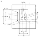
- FIG. 3 is a schematic plan view for explaining a method of manufacturing the semiconductor device shown in FIG.
- FIG. 4 is a schematic cross-sectional view of the line segment IV-IV of FIG.
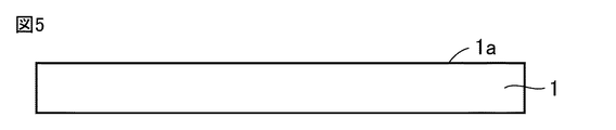
- FIG. 5 is a schematic cross-sectional view for explaining the manufacturing method of the semiconductor device shown in FIG. 6 to 9 are schematic cross-sectional views for explaining the manufacturing method of the semiconductor device shown in FIG.
- a method of manufacturing a semiconductor device according to the present embodiment will be described with reference to FIGS. 1 to 9.
- the semiconductor device 4 as shown in FIG. 2 can be obtained.
- the semiconductor device 4 shown in FIG. 2 includes a substrate 1 and a semiconductor element 3 connected to the substrate 1 via a bonding layer 2.
- the bonding layer 2 is a member formed by drying the sinterable metal bonding material 22 (see FIG. 6) and then heating it while applying pressure, as will be described later.
- the semiconductor element 3 is fixed to the substrate 1 in the bonding layer 2.
- the metal mask 6 and the squeegee 9 as shown in FIGS. 3 and 4 are used.
- the metal mask 6 includes a first surface 6a and a second surface 6b with which the squeegee 9 comes into contact.
- the second surface 6b is located on the opposite side of the first surface 6a.
- the second surface 6b faces the surface 1a of the substrate 1.
- An opening 7 is formed in the metal mask 6.
- the opening 7 is formed so as to reach from the first surface 6a to the second surface 6b.
- the first surface 6a of the metal mask 6 is formed with a recess 8 that surrounds the opening 7 and is connected to the opening 7.
- the metal mask 6 When the metal mask 6 is arranged on the surface 1a of the substrate 1, the surface portion 1aa of the substrate 1 is exposed inside the opening 7. As will be described later, the sinterable metal bonding material 22 is supplied to the surface portion 1aa. As shown in FIG. 3, the total width W2 of the recess 8 and the opening 7 is smaller than the length W3 of the squeegee 9. As shown in FIG. 4, a groove 10 is formed around the opening 7 on the second surface 6b of the metal mask 6.
- FIG. 1 The method for manufacturing the semiconductor device shown in FIG. 1 is carried out using such a metal mask 6 and a squeegee 9. This will be described in detail below.
- FIG. 6, which will be described later, illustrates a case where a configuration in which only one opening 7 is formed is used as the metal mask 6 for the sake of simplicity.
- the preparation step (S1) is first carried out.
- the substrate 1 constituting the semiconductor device is prepared.
- the substrate 1 includes, for example, a metal substrate containing copper (Cu), aluminum (Al), or the like, or an insulating property made of aluminum oxide (Al 2 O 3 ), silicon nitride (Si 3 N 4 ), aluminum nitride (Al N), or the like.
- a ceramic insulating substrate or the like in which a conductor layer made of a metal such as copper or aluminum is laminated and fixed to the ceramic substrate can be used.
- the conductor layer constituting the ceramic insulating substrate described above may be a metal layer composed of a single layer, or a composite layer in which a conductive coating layer is formed on the surface of the base conductor layer. You may.
- the material of the base conductor layer for example, copper or aluminum can be used.
- a noble metal such as silver (Ag) or gold (Au) can be used.
- a ceramic substrate made of silicon nitride, in which copper plates as conductor layers are connected to both sides, may be used.
- the copper plate may be fixed to the ceramic substrate by a brazing material as a joining material.
- a brazing material an Ag-Cu-Ti brazing material containing silver and copper as main components and titanium (Ti) added as an activator may be used.
- the thickness of the ceramic substrate described above may be, for example, 0.3 mm.
- the thickness of the copper plate may be, for example, 0.4 mm.
- the joining material supply process (S2) is carried out.
- the sinterable metal bonding material 22 is supplied onto the surface 1a of the substrate 1 by using a screen printing method.
- the metal mask 6 having the opening 7 is arranged on the surface 1a of the substrate 1.
- the metal mask 6 has a thickness T1.
- the sinterable metal bonding material 22 is arranged inside the opening 7.
- the metal fine particles contained in the sinterable metal bonding material 22 are higher than the melting point of the metal constituting the metal fine particles.
- a metal bond between the semiconductor element 3 as a member to be joined and the substrate 1 is achieved.
- metal fine particles miniaturized to a nanometer-level size show a characteristic that a sintering reaction occurs even at room temperature.
- problems such as an increase in the size of the metal fine particles and a decrease in reactivity occur.
- the sinterable metal bonding material 22 contains metal fine particles and an organic solvent component that disperses the metal fine particles, and further covers the metal fine particles for the purpose of suppressing the sintering reaction at low temperature in the metal fine particles. A protective film is formed.
- the squeegee 9 is moved so as to pass over the opening 7 in a state of being in contact with the first surface 6a of the metal mask 6.
- the total length L3 of the recess 8 and the opening 7 in the moving direction of the squeegee 9 shown by the arrow 31 is such that the squeegee 9 contacts the contact region 6aa of the first surface 6a of the metal mask 6. It is longer than the distance L2 that is moved in the state of being moved. Further, the distance L2 is longer than the total length L1 of the openings 7 in the moving direction of the squeegee 9.
- the sinterable metal bonding material 22 is supplied to the surface portion 1aa of the substrate 1 exposed inside the opening 7.
- the step (S2) since the recess 8 is formed in the metal mask 6, as can be seen from FIGS. 3 and 6, the surface portion 1aa of the substrate 1 to which the sinterable metal bonding material 22 is supplied is seen in a plan view. And the contact area 6aa with which the squeegee 9 comes into contact with the metal mask 6 are arranged at intervals.
- the metal mask 6 is removed from the surface 1a of the substrate 1.
- the sinterable metal bonding material 22 having a thickness T1 can be supplied on the surface 1a of the substrate 1.
- the thickness T1 of the sinterable metal bonding material 22 can be, for example, 30 ⁇ m or more and 200 ⁇ m or less.
- the drying step (S3) is carried out.
- the sinterable metal bonding material 22 supplied to the surface portion 1aa of the substrate 1 is dried by heating.
- the dried sintered metal bonding material 22a in which the organic component has volatilized to some extent is arranged on the surface 1a of the substrate 1.
- the drying temperature can be 80 ° C. or higher and 200 ° C. or lower, and the drying time can be 1 minute or longer and 60 minutes or lower.
- the temporary fixing step (S4) is carried out.
- the semiconductor element 3 is mounted on the sinterable metal bonding material 22a after drying.
- the semiconductor element 3 for example, a semiconductor element 3 using silicon (Si) can be used.
- a metallized back electrode is formed on the back surface of the semiconductor element 3 that comes into contact with the dried sinterable metal bonding material 22a.
- the semiconductor element 3 is heated while being pressed toward the substrate 1.
- the heating time at this time is shorter than the heating time in the joining step (S5) described later.
- the pressure for pressing the semiconductor element 3 at this time is also smaller than the pressure in the joining step (S5) described later.
- the heating temperature can be 25 ° C. or higher and 200 ° C. or lower
- the pressing pressure can be 0.01 MPa or higher and 5 MPa or lower
- the pressing time can be 0 minutes or longer and 1 minute or lower.
- Silicon (Si) may be used as the material constituting the semiconductor element 3, but a so-called wide band having a wider band gap than silicon, such as silicon carbide (SiC), gallium nitride (GaN), or diamond, is used. Gap semiconductor materials may be applied.
- the device type of the semiconductor element 3 is not particularly limited, but a switching element such as an IGBT (Insulated Gate Bipolar Transistor) or a MOSFET (metal-oxide-semiconductor field-effect transistor), or a rectifying element such as a diode is used as a semiconductor element. It can be used as 3.
- the planar shape of the semiconductor element 3 can be, for example, a rectangle having a side of 5 mm or more and 20 mm or less.
- silicon (Si) when silicon (Si) is used as the material of the semiconductor element 3 that functions as a switching element or a rectifying element, it is lower than that of a semiconductor element using silicon carbide (SiC), for which the application of sinterable metal bonding is advancing. Because of the cost, it is possible to reduce the price of the power module to which the semiconductor device according to the present embodiment is applied. Further, since the bonding using the sinterable metal bonding material 22 (sinterable metal bonding) has higher heat dissipation than the conventional solder bonding, the semiconductor device 4 can be operated at a high temperature. However, silicon (Si) has lower bending strength and hardness than silicon carbide (SiC).
- silicon (Si) may be used as the material of the semiconductor element 3.
- the size of the semiconductor element 3 can be 15 mm in length ⁇ 15 mm in width, and the thickness can be 0.15 mm.
- the joining step (S5) is carried out.
- the sinterable metal bonding material 22a after drying is bonded to the bonding layer 2 by heating while pressing the semiconductor element 3 toward the substrate 1 with a pressure higher than the pressing pressure in the step (S4). (See Fig. 2). That is, in the step (S5), the semiconductor element 3 is bonded to the substrate 1 via the sinterable metal bonding material 22a after drying.
- the heating temperature in the step (S5) may be higher than the heating temperature in the step (S4). Further, the heating temperature in the step (S5) is lower than the melting point of the metal constituting the metal fine particles contained in the sinterable metal bonding material 22.
- the heating temperature can be 250 ° C. or higher and 350 ° C. or lower
- the pressing pressure can be 0.1 MPa or higher and 50 MPa or lower
- the pressing time can be 1 minute or longer and 60 minutes or lower.
- the metal fine particles are diffusion-bonded. Further, the back surface electrode of the semiconductor element 3 and the bonding layer 2 are diffusion-bonded. Further, the surface 1a of the substrate 1 and the bonding layer 2 are also diffusively bonded. As a result, the melting point of the bonding layer 2 becomes the melting point of the metal constituting the bonding layer 2. As a result, in the obtained semiconductor device 4, the heat resistant temperature can be made higher than the heating temperature in the step (S5). In this way, the semiconductor device 4 shown in FIG. 2 can be obtained.
- the post-treatment step (S6) is carried out.
- a lead electrode is connected to the semiconductor element 3
- a frame (not shown) is connected to the semiconductor device 4 using, for example, an adhesive, and the semiconductor element 3 is embedded inside the frame. Perform necessary steps such as arranging the sealing resin. In this way, the semiconductor module can be obtained.
- sealing resin a resin obtained by embedding a semiconductor element 3 or the like with a gel resin and then curing the gel resin may be used.
- the periphery of the semiconductor element 3 may be resin-sealed by another method such as sealing by silicone potting or molding. Alternatively, resin sealing may not be performed.
- Sinterable metal joints are non-pressurized sintered joints in which the sinterable metal joint material 22 is joined only by heating without pressurization, and pressure sintering in which the sinterable metal joint material is heated and joined while being pressurized. It is roughly divided into joining. In this embodiment, a pressure sintering joint will be used for description.
- the sinterable metal bonding material 22 contains metal fine particles having a nanometer level size as an aggregate. Nanometer-sized metal particles have a very large surface area relative to their volume and have a large amount of surface energy. Therefore, the reactivity of the above-mentioned metal fine particles is high. Therefore, in the bonding using the sinterable metal bonding material 22, the metal bonding between the metal fine particles proceeds by diffusion at a temperature lower than the melting point indicated by the metal constituting the metal fine particles in the state of the bulk material as described above. I am using the phenomenon.
- the material constituting the metal fine particles to be the aggregate may be a single metal classified into precious metals such as gold (Au), silver (Ag), copper (Cu), palladium (Pd), and platinum (Pt).
- precious metals such as gold (Au), silver (Ag), copper (Cu), palladium (Pd), and platinum (Pt).
- Ag—Pd alloy, Au—Si alloy, Au—Ge alloy, Au—Cu alloy and the like may be used as the material.
- Gold, silver, copper, etc., which are exemplified as materials constituting metal fine particles have a higher thermal conductivity than solder. Therefore, the thickness of the bonding layer 2 composed of the sinterable metal bonding material 22 can be made thinner than when solder is used, and high heat dissipation performance can be realized.
- the metal fine particles Due to its high reactivity, metal fine particles can be sintered, that is, diffusion bonded, by simply contacting each other even at room temperature. Therefore, in the sinterable metal bonding material 22, the metal fine particles are covered with an organic protective film in order to prevent the metal fine particles from aggregating and proceeding with the sintering reaction. Further, in order to make the plurality of metal fine particles independent, the plurality of metal fine particles are dispersed and held by the organic dispersant. That is, the sinterable metal bonding material 22 is a paste in which metal fine particles serving as an aggregate are dispersed in an organic component. At the time of joining, organic components such as an organic protective film and an organic dispersant volatilize, so that only the metal material remains. In the above-described embodiment, for example, silver (Ag) particles having a nanometer-level size may be used as the metal fine particles.
- a dispense supply method in which the sinterable metal bonding material 22 is supplied by air can be mentioned.
- the thickness of the bonding layer 2 is uniform, and the bonding with the sinterable metal bonding material 22 is achieved over the entire surface of the semiconductor element 3. Is preferable. Therefore, it is necessary to supply the sinterable metal bonding material 22 flatly on the surface 1a of the substrate 1.
- the sinterable metal bonding material 22 is supplied on the substrate 1 by using a screen printing method.
- the screen printing method the sinterable metal bonding material 22 can be supplied flatly on the substrate 1 in the same manner as the shape at the time of final bonding. Therefore, it is not necessary to crush the sinterable metal bonding material 22 supplied on the substrate 1 with the semiconductor element 3. Therefore, the step (S3) of volatilizing the solvent by heating in advance can be performed before the semiconductor element 3 is mounted on the sinterable metal bonding material 22.
- a semiconductor element 3 having a large size exceeding 10 mm in length ⁇ 10 mm in width can be bonded to the substrate 1 without causing problems such as voids and poor bonding.
- a recess 8 which is a thin region is formed around the opening 7.
- the thickness of the metal mask 6 in the region where the recess 8 is formed may be about 10% or more and 90% or less with respect to the thickness T1 of the metal mask 6 (see FIG. 6).
- the depth from the first surface 6a of the metal mask to the bottom of the recess 8 may be 10% or more and 90% or less of the thickness T1 of the metal mask 6.
- a metal mask 6 having a thickness T1 of 150 ⁇ m was used.
- the thickness of the region where the recess 8 was formed was 110 ⁇ m, that is, the depth of the recess 8 was 40 ⁇ m.
- Examples of the processing method of the metal mask 6 forming the concave portion 8 include a laser processing method and an etching method using a chemical reaction using a chemical solution or the like.
- the metal mask 6 may be processed by any of the above-mentioned methods or other methods.
- the material of the metal mask 6 is generally stainless steel, for example, but any other material may be used depending on the type of the sinterable metal bonding material 22. For example, nickel (Ni), aluminum (Al), copper (Cu), or the like may be used as the material of the metal mask 6. In the present embodiment, stainless steel is used as the material of the metal mask 6, and the recess 8 is formed by a laser processing method.
- the metal mask 6 provided with the opening 7 and the recess 8 can be manufactured, for example, by stacking two metal masks having openings having different areas on top and bottom, but one plate is formed by a laser processing method.
- a single metal mask may be produced by processing the shaped member.
- the accuracy of the thickness of the metal mask 6 can be improved.
- the manufacturing cost can be reduced by further improving the accuracy of the thickness of the sinterable metal bonding material 22 and reducing the man-hours for manufacturing the metal mask 6.
- the width W2 of the recess 8 is wider than the width W1 of the opening 7 of the metal mask 6 and narrower than the width W3 of the squeegee 9.
- the width W1 of the opening 7 of the metal mask 6 can be arbitrarily set depending on the product and is not limited to a specific value. Further, the width W3 of the squeegee 9 may be larger than the width W1 of the opening 7 of the metal mask 6.
- the width W3 of the squeegee 9 can be, for example, 10 mm or more and 10000 mm or less. In the present embodiment, the width W1 of the opening 7 of the metal mask 6 is 30 mm, and the width W3 of the squeegee 9 is 50 mm.
- the width W2 of the recess 8 is set to 40 mm. It should be noted that the effect of the present embodiment can be obtained if the above relationship is satisfied other than the above-mentioned values.
- the width W1 of the opening 7 means the width of the opening 7 when one opening 7 is formed inside the one recess 8 as shown in FIG. Further, when a plurality of openings 7 are formed inside one recess 8 as shown in FIG. 3, the width W1 of the openings 7 means the width of the region where the plurality of openings 7 are formed.
- the length of the recess 8 in the moving direction of the squeegee 9 may be longer than the distance L2 which is the driving range of the squeegee 9.
- the squeegee 9 is driven in the range of ⁇ 60 mm to +60 mm in the direction indicated by the arrow 31 which is the moving direction of the squeegee 9 from the center C of the region where the opening 7 is formed in the metal mask 6. That is, the distance L2 was set to 120 mm.
- the recess 8 is formed in the range of -100 mm to +100 mm in the direction indicated by the arrow 31 from the center C of the region where the opening 7 is formed in the metal mask 6. From a different point of view, the length L3 was set to 200 mm.
- a groove 10 is formed around the opening 7 by a half-etching process as described above.
- the groove portion 10 plays a role of preventing the sinterable metal bonding material 22 from oozing out between the metal mask 6 and the substrate 1 during screen printing of the sinterable metal bonding material 22.
- the squeegee 9 is made of a metal plate such as stainless steel or aluminum (Al), a metal plate made of stainless steel or the like on which a plating layer such as nickel (Ni) is formed, or a resin such as urethane rubber or polyester.
- a plate material may be used.
- the material of the squeegee 9 can be arbitrarily selected according to the material of the sinterable metal bonding material 22 and the supply area of the sinterable metal bonding material 22. Further, the thickness, width, hardness and the like of the squeegee 9 can be arbitrarily set.
- a plate material made of polyester resin having a thickness of 0.2 mm is used as the squeegee 9 for example.
- squeegee 9 of other material and size may be used.
- the method for manufacturing a semiconductor device includes a step of preparing a substrate (S1), a step of supplying (S2), and a step of joining (S5).
- the sinterable metal bonding material 22 is supplied onto the surface 1a of the substrate 1.
- the joining step (S5) the semiconductor element 3 is joined to the substrate 1 via the sinterable metal bonding material 22a.
- a metal mask 6 having an opening 7 is placed on the surface 1a of the substrate 1, and a squeegee 9 is used to sintered the surface portion 1aa of the substrate 1 exposed inside the opening 7.
- the sex metal bonding material 22 is supplied.
- the surface portion 1aa of the substrate 1 to which the sinterable metal bonding material 22 is supplied and the contact region 6aa to which the squeegee 9 contacts in the metal mask 6 are arranged at intervals. Has been done.
- the sintered metal bonding material 22 is sandwiched between the open end of the opening 7 and the squeegee 9, and the shear stress is obtained. It is possible to suppress the occurrence of problems such as the formation of aggregates. As a result, it is possible to suppress the occurrence of a problem that the semiconductor element 3 constituting the semiconductor device 4 is damaged due to the presence of the agglomerates, and as a result, the reliability of the semiconductor device can be improved.
- the metal mask 6 includes a first surface 6a and a second surface 6b with which the squeegee 9 comes into contact.
- the second surface 6b is located on the opposite side of the first surface 6a and faces the surface 1a of the substrate 1.
- the opening 7 is formed so as to reach from the first surface 6a to the second surface 6b.
- the first surface 6a of the metal mask 6 is formed with a recess 8 that surrounds the opening 7 and is connected to the opening 7.
- the surface portion 1aa on which the sinterable metal bonding material 22 is arranged on the substrate 1 and the contact region 6aa on which the squeegee 9 contacts in the metal mask 6 are easily arranged at intervals. be able to.
- the thickness of the sinterable metal bonding material 22 located in the recess 8 is the depth of the recess 8. It can be thickened to some extent according to. Therefore, it is possible to suppress the occurrence of a problem that the organic component is completely volatilized from the sinterable metal bonding material 22 located in the recess 8 and the sinterable metal bonding material 22 is solidified.
- the positional relationship between the metal mask 6 and the squeegee 9 has a great influence on the supply amount of the sinterable metal bonding material 22 and the shape after the supply.
- the sinterable metal bonding material 22 cannot be supplied flat due to the warp of the substrate 1 and the inclination of the squeegee 9, and the sintering metal bonding material 22 cannot be supplied flatly. Supply amount is not stable.
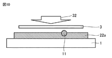
- FIGS. 10 and 11 are schematic views for explaining the effect of the method for manufacturing the semiconductor device shown in FIG.
- FIG. 10 shows a case where the agglomerates 11 are present in the sinterable metal bonding material 22a when the semiconductor element 3 is bonded.
- the agglomerate 11 is present in the sinterable metal bonding material 22
- the semiconductor element 3 is pressed as shown by an arrow 32 at the time of joining the semiconductor element 3
- the region in contact with the agglomerate 11 in the semiconductor element 3 is formed. Stress concentrates on.
- FIG. 11 in the semiconductor element 3, bending stress is generated starting from a portion in contact with the aggregate 11, and crack 12 is generated.
- the sinterable metal bonding material 22 on the metal mask 6 is poured into the opening 7 using the squeegee 9, a small amount of the sinterable metal bonding material 22 may remain on the metal mask 6. This is because even when the squeegee 9 and the metal mask 6 are brought into close contact with each other, a slight gap may be generated between the squeegee 9 and the metal mask 6, and the sintered metal bonding material 22 may remain in the gap. Is.
- the remaining sinterable metal bonding material 22 has a very thin coating film having a thickness of, for example, 1 ⁇ m or more and 10 ⁇ m or less.
- the organic components and the like contained therein are likely to volatilize. That is, after supplying the sinterable metal bonding material 22 onto the substrate 1 using the squeegee 9, a part of the sinterable metal bonding material 22 thinly coated on the surface of the metal mask 6 takes only a short time. Organic components volatilize. As a result, the part of the sinterable metal bonding material 22 may solidify from the paste state to become the core of the agglomerate 11.
- the metal mask 6 is provided with a recess 8.
- the metal mask 6 and the squeegee 9 can be brought into contact with each other with a force of, for example, 1 kgf or more and 30 kgf or less to stabilize the supply amount of the sintered metal bonding material 22.
- the recess 8 prevents the edge of the opening 7 in the metal mask 6 from coming into contact with the squeegee 9, and prevents the generation of agglomerates 11 of metal fine particles.
- the sintered metal bonding material 22 is thickly applied to the recess 8 by the difference between the thickness T1 of the metal mask 6 and the thickness of the metal mask 6 at the portion where the recess 8 is formed (that is, the depth of the recess 8). ing. Therefore, in the sinterable metal bonding material 22 arranged in the recess 8, the volatilization of the organic component is suppressed, and the solidification of the sinterable metal bonding material 22 can be suppressed.
- the supply amount of the sinterable metal bonding material 22 changes depending on the positional relationship between the metal mask 6 and the squeegee 9.
- the position of the metal mask 6 changes due to the warp of the substrate 1 or the like, so that the supply amount of the sinterable metal bonding material 22 becomes large.
- the supply amount of the sintered metal bonding material 22 is constant, but the wide edge region of the opening 7 of the metal mask 6 and the squeegee 9 are in contact with each other. , Aggregates 11 increase.
- the metal mask 6 and the squeegee 9 are brought into contact with each other on the outside of the recess 8, and the edge of the opening 7 of the metal mask 6 and the squeegee 9 are not in contact with each other. Screen printing of the conductive metal bonding material 22 is possible. Therefore, the supply amount of the sinterable metal bonding material 22 can be kept constant while suppressing the generation of the agglomerates 11.
- the total width W2 of the recess 8 and the opening 7 is smaller than the length W3 of the squeegee 9. In this case, when the screen printing method is performed, the squeegee 9 can be surely brought into contact with the first surface 6a of the metal mask 6 on the outside of the recess 8.
- the total length L3 of the recess 8 and the opening 7 in the moving direction of the squeegee 9 is such that the squeegee 9 is a contact region of the first surface 6a of the metal mask 6. It is longer than the distance L2 moved in contact with 6aa.
- the operation start point 71 of the squeegee 9 in the moving direction of the squeegee 9 is a recess 8 located on one side of the opening 7 in the moving direction. It is placed at a position that overlaps with.
- the operation end point 72 of the squeegee 9 in the moving direction is arranged at a position overlapping the recess 8 located on the opposite side of the opening 7 in the moving direction.
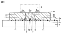
- the recess 8 is formed outside the edge of the opening 7 in the moving direction of the squeegee 9, it is certain that the squeegee 9 comes into contact with the edge of the opening 7 when performing the screen printing method. Can be prevented.
- FIG. 12 is a schematic view showing a squeegee used in the method for manufacturing a semiconductor device according to the second embodiment.
- 13 and 14 are schematic views for explaining the manufacturing method of the semiconductor device according to the second embodiment.
- FIG. 13 shows a step of applying the sinterable metal bonding material 22 to the surface of the substrate 1 by using a screen printing method in the step (S2) shown in FIG.
- FIG. 14 shows with reference to FIGS. 12 to 14 in which the sinterable metal bonding material 22 is arranged on the surface of the substrate 1 by removing the metal mask 6 from the substrate 1 after the step shown in FIG. , The method of manufacturing the semiconductor device according to the second embodiment will be described.
- the method for manufacturing the semiconductor device according to the second embodiment basically has the same configuration as the method for manufacturing the semiconductor device according to the first embodiment, but the metal used in the bonding material supply step (S2) shown in FIG.
- the configurations of the mask 6 and the squeegee 9 are different from the manufacturing method of the semiconductor device according to the first embodiment. That is, in the squeegee 9 used in the method for manufacturing the semiconductor device according to the second embodiment, the squeegee recess 14 having a depth T2 is formed in the middle portion of the end face facing the metal mask 6 in the supply step (S2). There is. As shown in FIG.
- the width W5 of the squeegee recess 14 is larger than the individual width W4 of the opening 7, and the width W5 of the squeegee recess 14 is the width W1 of the opening 7 shown in FIG. It is larger than the width of the region where the opening 7 is formed).
- the end portions 9a located on both sides of the squeegee recess 14 on the end surface of the squeegee 9 come into contact with the contact region 6aa of the metal mask 6.
- the metal mask 6 used in the method for manufacturing a semiconductor device according to the second embodiment has an opening 7 formed as shown in FIG. 13, but unlike the metal mask 6 shown in FIG. 4, the recess 8 (FIG. 4). See) is not formed. That is, in the metal mask 6 shown in FIG. 13, the opening 7 is formed so as to penetrate from the first surface 6a to the second surface 6b, and the opening width and the second surface of the opening 7 on the first surface 6a. The opening width of the opening 7 in 6b is substantially the same.
- the contact region 6aa of the metal mask 6 with which the end portion 9a of the squeegee 9 contacts is arranged so as to sandwich the opening 7 as shown in FIG.
- the contact region 6aa is arranged so as to sandwich the opening 7 in the width direction (direction indicated by the arrow 33 in FIG. 13) orthogonal to the moving direction of the squeegee 9 in the step (S2).
- the contact area 6aa is spaced apart from the opening 7. That is, the end surface of the squeegee 9 does not come into contact with the edge portion 7a of the opening 7 on the first surface 6a.
- the depth T2 of the squeegee recess 14 in the squeegee 9 shall be sufficiently large so that the squeegee 9 does not come into contact with the edge 7a of the opening 7 of the metal mask 6 even if the squeegee 9 is deformed in the step (S2). Is preferable.
- the total thickness T3 of the thickness T1 of the metal mask 6 (that is, the depth of the opening 7) and the depth T2 of the squeegee recess 14 is applied by the step (S2).
- the depth T2 of the squeegee recess 14 can be, for example, 50 ⁇ m.
- the thickness T1 of the metal mask 6 can be set to, for example, 100 ⁇ m. In this case, the thickness of the supplied sinterable metal bonding material 22 is 150 ⁇ m.
- any method such as mechanical polishing, laser processing, or etching with a chemical solution can be used.
- the amount of deformation of the squeegee 9 is directly linked to the supply stability of the sinterable metal bonding material 22. Therefore, as the material of the squeegee 9, it is desirable to use a material having as high hardness as possible and little deformation.
- a plate material made of stainless steel having a thickness of about 1 mm can be used as the material of the squeegee 9.
- the step (S2) shown in FIG. 3 is carried out using the metal mask 6 and the squeegee 9 shown in FIGS. 12 and 13, and the other steps (S1) and steps (S3) to (S6) are carried out.
- the semiconductor device according to the present embodiment can be obtained by carrying out the same as the method for manufacturing the semiconductor device according to 1.
- the squeegee 9 is formed with a squeegee recess 14 in the middle of an end surface facing the metal mask 6 in the supply step (S2) shown in FIG.
- the width W5 of the squeegee recess 14 is larger than the width W4 of the opening 7.
- the ends 9a located on both sides of the squeegee recess 14 on the end face of the squeegee 9 are with the contact region 6aa of the metal mask 6. Contact.
- the contact region 6aa is arranged so as to sandwich the opening 7 and is separated from the opening 7.
- the surface portion 1aa and the metal mask 6 on which the sinterable metal bonding material 22 is arranged on the substrate 1 by forming the squeegee recess 14 are formed in the same manner as in the method for manufacturing the semiconductor device according to the first embodiment.
- the contact area 6aa with which the squeegee 9 comes into contact with the squeegee 9 can be arranged at a distance from each other.
- the sintered metal bonding material 22 is sandwiched between the edge portion 7a of the opening 7 and the squeegee 9 and receives shear stress.
- the width W5 of the squeegee recess 14 is larger than the width W4 of the opening 7 in the width direction orthogonal to the moving direction of the squeegee 9.
- the contact region 6aa where the end portion 9a of the squeegee 9 contacts the metal mask 6 can be easily arranged at a position away from the opening 7.
- the metal mask 6 includes a first surface 6a and a second surface 6b.
- the squeegee 9 comes into contact with the first surface 6a.
- the second surface 6b is located on the opposite side of the first surface 6a and faces the surface 1a of the substrate 1.
- the opening 7 is formed so as to reach from the first surface 6a to the second surface 6b.
- the end surface of the squeegee 9 does not come into contact with the edge portion 7a of the opening 7 in the first surface 6a.
- FIG. 15 is a schematic plan view of the semiconductor device according to the third embodiment.
- FIG. 16 is a schematic cross-sectional view of the line segment XVI-XVI of FIG.
- FIG. 17 is a schematic plan view for explaining a substrate of the semiconductor device according to the third embodiment.
- the semiconductor device 41 shown in FIGS. 15 to 17 mainly includes a substrate 1, a protective film 5, a sinterable metal bonding material 22, and a semiconductor element 3.
- the substrate 1 includes a surface 1a.
- the surface 1a includes a surface portion 1aa to which the sinterable metal bonding material 22 is supplied, a region 1ab to be soldered in a subsequent step, and a region 1ac covered with the protective film 5.
- the region 1ac is a region other than the surface portion 1aa and the region 1ab on the surface 1a.
- the material constituting the protective film 5 is, for example, solder resist.
- the semiconductor element 3 is bonded to the surface 1a of the substrate 1 by the sinterable metal bonding material 22.
- the protective film 5 is formed for the purpose of limiting the area where the solder spreads when the terminals are soldered to the substrate 1 in a subsequent process.
- the thickness T4 of the protective film 5 may be, for example, 0.001 mm or more and 0.5 mm or less, or 0.005 mm or more and 0.3 mm or less.
- the thickness T4d of the protective film 5 may be, for example, 0.01 mm.
- the semiconductor device 41 includes four semiconductor elements 3 on the substrate 1.
- a plurality of semiconductor elements 3 may be arranged on the substrate 1, or one semiconductor element 3 may be arranged on the substrate 1.
- the number, type, shape, and arrangement of the semiconductor elements 3 can be arbitrarily determined according to the characteristics required for the semiconductor device 41, and are not limited to the configurations shown in FIGS. 15 to 17. Needless to say, the effects of the present disclosure can be obtained even when the number, type, shape, and arrangement of the semiconductor elements 3 in the semiconductor device 41 are different from the configurations shown in FIGS. 15 to 17.
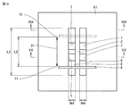
- FIG. 18 is a schematic plan view showing a metal mask used in the method for manufacturing a semiconductor device according to the third embodiment.
- FIG. 19 is a schematic cross-sectional view of the line segment XIX-XIX of FIG.
- FIG. 20 is a schematic cross-sectional view taken along the line segments XX-XX of FIG. 21 to 23 are schematic views for explaining the manufacturing method of the semiconductor device according to the third embodiment.
- the semiconductor device manufacturing method according to the present embodiment basically has the same configuration as the semiconductor device manufacturing method shown in FIG. 1, but is used in the bonding material supply step (S2) shown in FIG.
- the configuration of the metal mask 61 is different from the manufacturing method of the semiconductor device shown in FIG. That is, in the metal mask 61 shown in FIGS. 18 to 20, the shape of the recess 8 is different from that of the metal mask 6 shown in FIGS. 3 and 4.
- a specific description will be given.
- the metal mask 61 shown in FIGS. 18 to 20 has a first surface 6a with which the squeegee 9 contacts and a first surface 6a located on the opposite side of the first surface 6a. It has two sides 6b.
- an opening 7 penetrating from the first surface 6a to the second surface 6b is formed.
- the position and size of the opening 7 are the same as the position and size of the surface portion 1aa of the substrate 1.
- the surface portion 1aa of the substrate 1 is filled with the sinterable metal bonding material 22 in a state where the metal mask 6 is arranged on the surface 1a of the substrate 1 so that the surface portion 1aa is exposed.
- the sinterable metal bonding material 22 can be selectively supplied to the vehicle.
- a groove 10 is formed around the opening 7 on the second surface 6b of the metal mask 61.
- the planar shape of the concave portion 8 provided on the first surface 6a of the metal mask 61 is different from the planar shape of the concave portion 8 of the metal mask 6 shown in FIGS. 3 and 4.
- a recess 8 is formed on the first surface 6a so as to sandwich the opening 7 in the moving direction of the squeegee 9 indicated by the arrow 31, as shown in FIGS. 18 and 19.
- the width W4 of the recess 8 is the same as the width W4 of the opening 7 (see FIG. 20).
- the total length of the recess 8 and the opening 7 is the length L3.
- the distance between both ends of the recess 8 is the length L3 in the moving direction of the squeegee 9 shown by the arrow 31.
- the length L3 is longer than the distance L2 moved while the squeegee 9 is in contact with the contact region 6aa of the first surface 6a of the metal mask 61.
- the width W4 is, for example, 15 mm
- the length L3 is, for example, 250 mm
- the distance L2 is, for example, 100 mm.
- the thickness of the metal mask 61 is the same as the thickness T1 of the metal mask 6 shown in FIG.
- the depth of the metal mask 61 from the first surface 6a to the bottom of the recess 8 is the same as the depth of the metal mask 6 from the first surface 6a to the bottom of the recess 8.
- the metal mask 61 is pressed by the squeegee 9 against the substrate 1 with a force of 1 kgf or more and 30 kgf or less.
- the second surface 6b of the above is in close contact with the surface of the protective film 5 of the substrate 1.
- the force for pressing the squeegee 9 toward the substrate 1 may be 5 kgf.
- the viscosity of the sinterable metal bonding material 22 used in the present embodiment may be 30 Pa ⁇ s. Needless to say, the lower the viscosity, the more likely the capillary phenomenon occurs, and the more easily the sinterable metal bonding material 22 bleeds into the gap.
- contact regions 6aa in contact with the squeegee 9 exist in the vicinity of the opening 7 and at both ends in the width direction. Therefore, the metal mask 61 and the surface of the protective film 5 of the substrate 1 (or the surface 1a of the substrate 1 when the protective film 5 is not formed) can be brought into close contact with each other. As a result, there is no gap between the surface of the protective film 5 of the substrate 1 and the second surface 6b of the metal mask 61 (or between the surface 1a of the substrate 1 and the second surface 6b of the metal mask 61).
- the sinterable metal bonding material 22 can be filled in the opening 7. As a result, it is possible to prevent a part 22b of the sintered metal bonding material 22 from extending (bleeding) on the region other than the surface portion 1aa on the substrate 1, that is, on the protective film 5 such as solder resist.
- the method for manufacturing a semiconductor device includes a step of preparing a substrate (S1), a step of supplying (S2), and a step of joining (S5).
- the sinterable metal bonding material 22 is supplied onto the surface 1a of the substrate 1.
- the joining step (S5) the semiconductor element 3 is joined to the substrate 1 via the sinterable metal bonding material 22.
- a metal mask 6 having an opening 7 is placed on the surface 1a of the substrate 1, and a squeegee 9 is used to sintered the surface portion 1aa of the substrate 1 exposed inside the opening 7.
- the sex metal bonding material 22 is supplied.
- the contact regions 6aa that the squeegee 9 contacts in the metal mask 6 are arranged only on both sides of the opening 7 in the width direction orthogonal to the moving direction of the squeegee 9.
- the sinterable metal bonding material 22 is fixed on the substrate 1 by directly achieving metal bonding with the metal exposed on the surface portion 1aa of the substrate 1 by heating and pressurizing.
- a part 22b of the sintered metal bonding material 22 that has exuded onto the protective film 5 on the substrate 1 is not bonded because the protective film 5 prevents the bonding with the substrate 1. That is, a part 22b of the sintered metal bonding material 22 that has exuded onto the protective film 5 may peel off and become a conductive foreign substance in a subsequent process. Conductive foreign matter may cause insulation failure and deteriorate the performance of the semiconductor device 41.
- the metal mask 61 includes a first surface 6a and a second surface 6b with which the squeegee 9 comes into contact.
- the second surface 6b is located on the opposite side of the first surface 6a and faces the surface 1a of the substrate 1.
- the opening 7 is formed so as to reach from the first surface 6a to the second surface 6b.
- the first surface 6a of the metal mask 61 is formed with a recess 8 that sandwiches the opening 7 in the moving direction of the squeegee 9 and is connected to the opening 7.
- the width W4 of the opening 7 in the width direction orthogonal to the moving direction of the squeegee 9 is the same as the width W4 of the recess 8 in the width direction (see FIG. 19).
- the first surface 6a of the metal mask 6 can be arranged at intervals.
- the total length L3 of the recess 8 and the opening 7 in the moving direction of the squeegee 9 is such that the squeegee 9 is a contact region of the first surface 6a of the metal mask 61. It is longer than the distance L2 moved in contact with 6aa.
- the operation start point 71 of the squeegee 9 in the moving direction of the squeegee 9 is a recess 8 located on one side of the opening 7 in the moving direction. It is placed at a position that overlaps with.
- the operation end point 72 of the squeegee 9 in the moving direction is arranged at a position overlapping the recess 8 located on the opposite side of the opening 7 in the moving direction.
- the recess 8 is formed outside the edge of the opening 7 in the moving direction of the squeegee 9, it is certain that the squeegee 9 comes into contact with the edge of the opening 7 when performing the screen printing method. Can be prevented.
- the joining step (S5) is a semiconductor element on the sintered metal bonding material 22 supplied to the surface portion 1aa of the substrate 1 in the supplying step (S2). 3 includes a step of joining. In this case, it is possible to obtain a semiconductor device in which the semiconductor element 3 is bonded on the sinterable metal bonding material 22.
- Example Sample of Example: As a substrate, a ceramic substrate made of silicon nitride, in which copper plates as conductor layers were connected to both sides, was prepared. The copper plate is fixed to the ceramic substrate by a brazing material. As the brazing material, an Ag-Cu-Ti-based brazing material containing silver and copper as main components and titanium (Ti) added as an activator was used. The thickness of the ceramic substrate described above was 0.3 mm, and the thickness of the copper plate was 0.4 mm.
- a sinterable metal bonding material using nanometer-level size silver (Ag) particles as metal fine particles was prepared. Further, as the metal mask 6 and the squeegee 9, the metal mask 6 and the squeegee 9 having the configuration used in the method for manufacturing the semiconductor device according to the first embodiment were prepared. Specifically, stainless steel was used as the material of the metal mask 6. The thickness T1 of the metal mask 6 was 150 ⁇ m, the depth of the recess 8 was 40 ⁇ m, and the planar shape of the opening 7 was a square shape of 30 mm ⁇ 30 mm. The width W2 (see FIG.
- the recess 8 in the width direction orthogonal to the moving direction of the squeegee 9 was set to 40 mm.
- the recess 8 is formed in the range of -100 mm to +100 mm from the center of the opening 7. That is, the length L3 (see FIG. 3) of the recess 8 in the moving direction of the squeegee 9 is set to 200 mm.
- a plate material made of polyester resin having a thickness of 0.2 mm was used as the squeegee 9.
- the length W3 of the squeegee 9 was set to 50 mm.
- the substrate, the sinterable metal bonding material, and the squeegee 9 were the same as the samples of the above-mentioned Examples.
- the metal mask of the sample of the conventional example a metal mask having basically the same structure as the metal mask of the sample of the above-mentioned example but not having the recess 8 formed was prepared.
- 100 substrates were prepared.
- ⁇ Test method> Using each of the sample of the example and the sample of the conventional example, the sintered metal bonding material was applied to the surface of the substrate by the screen printing method using the metal mask 6 and the squeegee 9 described above. Then, a drying step was carried out. Next, the surface of the sinterable metal joint was photographed, and the size and number of the agglomerates formed were measured by image processing.
- the sinterable metal bonding material was specifically applied by the screen printing method as follows.
- the sinterable metal bonding material is supplied in the vicinity of the opening 7 of the metal mask and on the recess 8.
- the metal mask 6 and the squeegee 9 are brought into contact with each other at a place other than the recess 8 with a pressing force of 3 kgf.
- the squeegee 9 stands by at a position of -60 mm on one side (front side) in the moving direction of the squeegee 9 from the center of the opening 7 of the metal mask 6.
- the squeegee 9 is driven toward the opening 7 of the metal mask 6 at a speed of 50 mm / s to a position of the other side (back side) + 60 mm in the moving direction of the squeegee 9. After that, the squeegee 9 is driven again in the opposite direction from the position of +60 mm on the back side to the position of -60 mm on the front side. In this way, the squeegee 9 is reciprocated to fill the opening 7 of the metal mask 6 in both directions with the sinterable metal bonding material.
- the sinterable metal bonding material is supplied on the surface of the metal mask in the vicinity of the opening 7 of the metal mask. After that, the squeegee 9 is driven in the same manner as in the case of the sample of the above-mentioned example.
- the metal mask 6 is separated from the substrate 1 by lowering the substrate by 0.3 mm at, for example, 100 mm / s.
- the sinterable metal bonding material is supplied on the substrate.
- the substrate to which the sinterable metal bonding material 22 is supplied is heated, and a drying step of volatilizing excess organic components contained in the sinterable metal bonding material is carried out.
- the conditions for the drying step were a heating temperature of 100 ° C. and a drying time of 30 minutes.
- FIG. 24 is a graph showing the relationship between the number and size of agglomerates with respect to the samples of Examples and Comparative Examples.
- the vertical axis indicates the number of detected aggregates
- the horizontal axis indicates the classification of the size of the aggregates.
- the number of aggregates having a size of 50 ⁇ m or more and less than 100 ⁇ m is shown on the left side
- the number of aggregates having a size of 100 ⁇ m or more is shown on the right side.
- FIG. 24 shows the number of agglomerates generated per 100 substrates. In FIG.
- the data of the sample of the conventional example is shown by a bar graph with hatching of a diagonal line downward to the right, and the data of the sample of the example is shown by a bar graph with hatching of a diagonal line downward to the left.
- the sample of the example of the present disclosure suppresses the generation of aggregates as compared with the sample of the conventional example.
Landscapes
- Engineering & Computer Science (AREA)
- Manufacturing & Machinery (AREA)
- Microelectronics & Electronic Packaging (AREA)
- Die Bonding (AREA)
- Electric Connection Of Electric Components To Printed Circuits (AREA)
Priority Applications (2)
| Application Number | Priority Date | Filing Date | Title |
|---|---|---|---|
| JP2021572959A JP7254216B2 (ja) | 2020-01-22 | 2020-08-13 | 半導体装置の製造方法 |
| CN202080093359.1A CN114981937A (zh) | 2020-01-22 | 2020-08-13 | 半导体装置的制造方法 |
Applications Claiming Priority (2)
| Application Number | Priority Date | Filing Date | Title |
|---|---|---|---|
| JP2020008140 | 2020-01-22 | ||
| JP2020-008140 | 2020-01-22 |
Publications (1)
| Publication Number | Publication Date |
|---|---|
| WO2021149286A1 true WO2021149286A1 (ja) | 2021-07-29 |
Family
ID=76991847
Family Applications (1)
| Application Number | Title | Priority Date | Filing Date |
|---|---|---|---|
| PCT/JP2020/030762 Ceased WO2021149286A1 (ja) | 2020-01-22 | 2020-08-13 | 半導体装置の製造方法 |
Country Status (3)
| Country | Link |
|---|---|
| JP (1) | JP7254216B2 (https=) |
| CN (1) | CN114981937A (https=) |
| WO (1) | WO2021149286A1 (https=) |
Cited By (1)
| Publication number | Priority date | Publication date | Assignee | Title |
|---|---|---|---|---|
| DE102024127732A1 (de) * | 2024-09-25 | 2026-03-26 | Infineon Technologies Ag | Schablonenmaske und verfahren zum bilden von verbindungsschichten auf einem substrat für ein halbleitermodul |
Citations (7)
| Publication number | Priority date | Publication date | Assignee | Title |
|---|---|---|---|---|
| JPS60124064U (ja) * | 1984-01-31 | 1985-08-21 | 松下電器産業株式会社 | はんだ層印刷用マスク |
| JPH06196516A (ja) * | 1992-10-26 | 1994-07-15 | Sanyo Electric Co Ltd | 半田塗布方法、半導体装置の製造方法およびスキージ |
| JPH08153962A (ja) * | 1994-11-28 | 1996-06-11 | Hitachi Ltd | 半田ペースト印刷方法及び半田ペースト印刷装置 |
| JPH1178274A (ja) * | 1997-09-10 | 1999-03-23 | Mitsui High Tec Inc | エラストマー塗布用マスク |
| JP2010143227A (ja) * | 2010-02-05 | 2010-07-01 | Bonmaaku:Kk | スクリーン印刷版 |
| JP2016127219A (ja) * | 2015-01-08 | 2016-07-11 | 三菱電機株式会社 | 半導体デバイスの製造方法および半導体デバイス |
| JP2016190182A (ja) * | 2015-03-31 | 2016-11-10 | Dowaエレクトロニクス株式会社 | 接合材の塗布方法 |
Family Cites Families (6)
| Publication number | Priority date | Publication date | Assignee | Title |
|---|---|---|---|---|
| JP3896285B2 (ja) * | 2002-01-24 | 2007-03-22 | 三菱電機株式会社 | 半導体装置の製造方法 |
| JP2008066344A (ja) * | 2006-09-04 | 2008-03-21 | Toyota Industries Corp | 多層基板と金属接合材料の印刷方法 |
| JP6265693B2 (ja) * | 2013-11-12 | 2018-01-24 | 三菱電機株式会社 | 半導体装置およびその製造方法 |
| TWI694558B (zh) * | 2015-09-07 | 2020-05-21 | 日商日立化成股份有限公司 | 接合體及半導體裝置 |
| JP6741548B2 (ja) * | 2016-10-14 | 2020-08-19 | 日本碍子株式会社 | 半導体製造装置用部材及びその製法 |
| DE112017007305B4 (de) * | 2017-03-24 | 2022-12-15 | Mitsubishi Electric Corporation | Verfahren zur Herstellung einer Halbleitervorrichtung und Halbleitervorrichtung |
-
2020
- 2020-08-13 CN CN202080093359.1A patent/CN114981937A/zh active Pending
- 2020-08-13 JP JP2021572959A patent/JP7254216B2/ja active Active
- 2020-08-13 WO PCT/JP2020/030762 patent/WO2021149286A1/ja not_active Ceased
Patent Citations (7)
| Publication number | Priority date | Publication date | Assignee | Title |
|---|---|---|---|---|
| JPS60124064U (ja) * | 1984-01-31 | 1985-08-21 | 松下電器産業株式会社 | はんだ層印刷用マスク |
| JPH06196516A (ja) * | 1992-10-26 | 1994-07-15 | Sanyo Electric Co Ltd | 半田塗布方法、半導体装置の製造方法およびスキージ |
| JPH08153962A (ja) * | 1994-11-28 | 1996-06-11 | Hitachi Ltd | 半田ペースト印刷方法及び半田ペースト印刷装置 |
| JPH1178274A (ja) * | 1997-09-10 | 1999-03-23 | Mitsui High Tec Inc | エラストマー塗布用マスク |
| JP2010143227A (ja) * | 2010-02-05 | 2010-07-01 | Bonmaaku:Kk | スクリーン印刷版 |
| JP2016127219A (ja) * | 2015-01-08 | 2016-07-11 | 三菱電機株式会社 | 半導体デバイスの製造方法および半導体デバイス |
| JP2016190182A (ja) * | 2015-03-31 | 2016-11-10 | Dowaエレクトロニクス株式会社 | 接合材の塗布方法 |
Cited By (1)
| Publication number | Priority date | Publication date | Assignee | Title |
|---|---|---|---|---|
| DE102024127732A1 (de) * | 2024-09-25 | 2026-03-26 | Infineon Technologies Ag | Schablonenmaske und verfahren zum bilden von verbindungsschichten auf einem substrat für ein halbleitermodul |
Also Published As
| Publication number | Publication date |
|---|---|
| CN114981937A (zh) | 2022-08-30 |
| JP7254216B2 (ja) | 2023-04-07 |
| JPWO2021149286A1 (https=) | 2021-07-29 |
Similar Documents
| Publication | Publication Date | Title |
|---|---|---|
| US11094664B2 (en) | Semiconductor device and method of manufacturing semiconductor device | |
| CN111316408B (zh) | 电力用半导体装置以及电力用半导体装置的制造方法 | |
| JP6719643B2 (ja) | 半導体装置及びその製造方法 | |
| CN109616460B (zh) | 电力用半导体装置 | |
| CN107210233B (zh) | 半导体器件及其制造方法 | |
| CN112786468B (zh) | 预成型扩散焊接 | |
| JP2018006492A (ja) | 半導体装置及び半導体装置の製造方法 | |
| JP2013209720A (ja) | 金属体の接合方法 | |
| US11101246B2 (en) | Semiconductor device having chips attached to support members through silver sintered bodies with particles | |
| JP2007019360A (ja) | 電子部品の実装方法 | |
| JP7254216B2 (ja) | 半導体装置の製造方法 | |
| JP2019216183A (ja) | 半導体装置、及び半導体装置の製造方法 | |
| WO2010134230A1 (ja) | 半導体装置及びその製造方法 | |
| JP2017005007A (ja) | 半導体装置、および半導体装置の製造方法 | |
| CN101304012B (zh) | 具有金属接触层的功率半导体基片及其制造方法 | |
| JP6258954B2 (ja) | 金属体の接合方法及び金属体の接合構造 | |
| CN115023804B (zh) | 电子器件和电子器件的制造方法 | |
| JP2014053406A (ja) | 半導体装置およびその製造方法 | |
| CN116830249A (zh) | 半导体装置及其制造方法 | |
| JP2023065215A (ja) | 半導体装置及びその製造方法 | |
| JP2003142972A (ja) | 電子部品装置の製造方法 | |
| TWI745572B (zh) | 電子零件安裝模組 | |
| JP2003031617A (ja) | 半導体装置の実装構造とその製造方法 | |
| JP2024131305A (ja) | 電力用半導体装置及びその製造方法 | |
| CN118136512A (zh) | 半导体模块的制造方法以及半导体模块 |
Legal Events
| Date | Code | Title | Description |
|---|---|---|---|
| 121 | Ep: the epo has been informed by wipo that ep was designated in this application |
Ref document number: 20915896 Country of ref document: EP Kind code of ref document: A1 |
|
| ENP | Entry into the national phase |
Ref document number: 2021572959 Country of ref document: JP Kind code of ref document: A |
|
| NENP | Non-entry into the national phase |
Ref country code: DE |
|
| 122 | Ep: pct application non-entry in european phase |
Ref document number: 20915896 Country of ref document: EP Kind code of ref document: A1 |