WO2021024083A1 - 半導体装置 - Google Patents
半導体装置 Download PDFInfo
- Publication number
- WO2021024083A1 WO2021024083A1 PCT/IB2020/057051 IB2020057051W WO2021024083A1 WO 2021024083 A1 WO2021024083 A1 WO 2021024083A1 IB 2020057051 W IB2020057051 W IB 2020057051W WO 2021024083 A1 WO2021024083 A1 WO 2021024083A1
- Authority
- WO
- WIPO (PCT)
- Prior art keywords
- circuit
- transistor
- memory
- data
- cpu
- Prior art date
- Legal status (The legal status is an assumption and is not a legal conclusion. Google has not performed a legal analysis and makes no representation as to the accuracy of the status listed.)
- Ceased
Links
Images


Classifications
-
- G—PHYSICS
- G06—COMPUTING OR CALCULATING; COUNTING
- G06F—ELECTRIC DIGITAL DATA PROCESSING
- G06F7/00—Methods or arrangements for processing data by operating upon the order or content of the data handled
- G06F7/38—Methods or arrangements for performing computations using exclusively denominational number representation, e.g. using binary, ternary, decimal representation
- G06F7/48—Methods or arrangements for performing computations using exclusively denominational number representation, e.g. using binary, ternary, decimal representation using non-contact-making devices, e.g. tube, solid state device; using unspecified devices
- G06F7/544—Methods or arrangements for performing computations using exclusively denominational number representation, e.g. using binary, ternary, decimal representation using non-contact-making devices, e.g. tube, solid state device; using unspecified devices for evaluating functions by calculation
- G06F7/5443—Sum of products
-
- H—ELECTRICITY
- H10—SEMICONDUCTOR DEVICES; ELECTRIC SOLID-STATE DEVICES NOT OTHERWISE PROVIDED FOR
- H10D—INORGANIC ELECTRIC SEMICONDUCTOR DEVICES
- H10D30/00—Field-effect transistors [FET]
- H10D30/60—Insulated-gate field-effect transistors [IGFET]
- H10D30/67—Thin-film transistors [TFT]
- H10D30/674—Thin-film transistors [TFT] characterised by the active materials
- H10D30/6755—Oxide semiconductors, e.g. zinc oxide, copper aluminium oxide or cadmium stannate
-
- G—PHYSICS
- G06—COMPUTING OR CALCULATING; COUNTING
- G06F—ELECTRIC DIGITAL DATA PROCESSING
- G06F12/00—Accessing, addressing or allocating within memory systems or architectures
-
- G—PHYSICS
- G11—INFORMATION STORAGE
- G11C—STATIC STORES
- G11C11/00—Digital stores characterised by the use of particular electric or magnetic storage elements; Storage elements therefor
- G11C11/21—Digital stores characterised by the use of particular electric or magnetic storage elements; Storage elements therefor using electric elements
- G11C11/34—Digital stores characterised by the use of particular electric or magnetic storage elements; Storage elements therefor using electric elements using semiconductor devices
- G11C11/40—Digital stores characterised by the use of particular electric or magnetic storage elements; Storage elements therefor using electric elements using semiconductor devices using transistors
- G11C11/401—Digital stores characterised by the use of particular electric or magnetic storage elements; Storage elements therefor using electric elements using semiconductor devices using transistors forming cells needing refreshing or charge regeneration, i.e. dynamic cells
- G11C11/403—Digital stores characterised by the use of particular electric or magnetic storage elements; Storage elements therefor using electric elements using semiconductor devices using transistors forming cells needing refreshing or charge regeneration, i.e. dynamic cells with charge regeneration common to a multiplicity of memory cells, i.e. external refresh
- G11C11/404—Digital stores characterised by the use of particular electric or magnetic storage elements; Storage elements therefor using electric elements using semiconductor devices using transistors forming cells needing refreshing or charge regeneration, i.e. dynamic cells with charge regeneration common to a multiplicity of memory cells, i.e. external refresh with one charge-transfer gate, e.g. MOS transistor, per cell
-
- G—PHYSICS
- G11—INFORMATION STORAGE
- G11C—STATIC STORES
- G11C11/00—Digital stores characterised by the use of particular electric or magnetic storage elements; Storage elements therefor
- G11C11/21—Digital stores characterised by the use of particular electric or magnetic storage elements; Storage elements therefor using electric elements
- G11C11/34—Digital stores characterised by the use of particular electric or magnetic storage elements; Storage elements therefor using electric elements using semiconductor devices
- G11C11/40—Digital stores characterised by the use of particular electric or magnetic storage elements; Storage elements therefor using electric elements using semiconductor devices using transistors
- G11C11/401—Digital stores characterised by the use of particular electric or magnetic storage elements; Storage elements therefor using electric elements using semiconductor devices using transistors forming cells needing refreshing or charge regeneration, i.e. dynamic cells
- G11C11/403—Digital stores characterised by the use of particular electric or magnetic storage elements; Storage elements therefor using electric elements using semiconductor devices using transistors forming cells needing refreshing or charge regeneration, i.e. dynamic cells with charge regeneration common to a multiplicity of memory cells, i.e. external refresh
- G11C11/405—Digital stores characterised by the use of particular electric or magnetic storage elements; Storage elements therefor using electric elements using semiconductor devices using transistors forming cells needing refreshing or charge regeneration, i.e. dynamic cells with charge regeneration common to a multiplicity of memory cells, i.e. external refresh with three charge-transfer gates, e.g. MOS transistors, per cell
-
- G—PHYSICS
- G11—INFORMATION STORAGE
- G11C—STATIC STORES
- G11C11/00—Digital stores characterised by the use of particular electric or magnetic storage elements; Storage elements therefor
- G11C11/21—Digital stores characterised by the use of particular electric or magnetic storage elements; Storage elements therefor using electric elements
- G11C11/34—Digital stores characterised by the use of particular electric or magnetic storage elements; Storage elements therefor using electric elements using semiconductor devices
- G11C11/40—Digital stores characterised by the use of particular electric or magnetic storage elements; Storage elements therefor using electric elements using semiconductor devices using transistors
- G11C11/401—Digital stores characterised by the use of particular electric or magnetic storage elements; Storage elements therefor using electric elements using semiconductor devices using transistors forming cells needing refreshing or charge regeneration, i.e. dynamic cells
- G11C11/4063—Auxiliary circuits, e.g. for addressing, decoding, driving, writing, sensing or timing
- G11C11/407—Auxiliary circuits, e.g. for addressing, decoding, driving, writing, sensing or timing for memory cells of the field-effect type
- G11C11/409—Read-write [R-W] circuits
-
- G—PHYSICS
- G11—INFORMATION STORAGE
- G11C—STATIC STORES
- G11C11/00—Digital stores characterised by the use of particular electric or magnetic storage elements; Storage elements therefor
- G11C11/54—Digital stores characterised by the use of particular electric or magnetic storage elements; Storage elements therefor using elements simulating biological cells, e.g. neuron
-
- G—PHYSICS
- G11—INFORMATION STORAGE
- G11C—STATIC STORES
- G11C14/00—Digital stores characterised by arrangements of cells having volatile and non-volatile storage properties for back-up when the power is down
-
- G—PHYSICS
- G11—INFORMATION STORAGE
- G11C—STATIC STORES
- G11C16/00—Erasable programmable read-only memories
- G11C16/02—Erasable programmable read-only memories electrically programmable
- G11C16/06—Auxiliary circuits, e.g. for writing into memory
- G11C16/10—Programming or data input circuits
-
- G—PHYSICS
- G11—INFORMATION STORAGE
- G11C—STATIC STORES
- G11C16/00—Erasable programmable read-only memories
- G11C16/02—Erasable programmable read-only memories electrically programmable
- G11C16/06—Auxiliary circuits, e.g. for writing into memory
- G11C16/26—Sensing or reading circuits; Data output circuits
-
- G—PHYSICS
- G11—INFORMATION STORAGE
- G11C—STATIC STORES
- G11C7/00—Arrangements for writing information into, or reading information out from, a digital store
- G11C7/10—Input/output [I/O] data interface arrangements, e.g. I/O data control circuits, I/O data buffers
- G11C7/1051—Data output circuits, e.g. read-out amplifiers, data output buffers, data output registers, data output level conversion circuits
- G11C7/1069—I/O lines read out arrangements
-
- G—PHYSICS
- G11—INFORMATION STORAGE
- G11C—STATIC STORES
- G11C7/00—Arrangements for writing information into, or reading information out from, a digital store
- G11C7/10—Input/output [I/O] data interface arrangements, e.g. I/O data control circuits, I/O data buffers
- G11C7/1078—Data input circuits, e.g. write amplifiers, data input buffers, data input registers, data input level conversion circuits
- G11C7/1096—Write circuits, e.g. I/O line write drivers
-
- G—PHYSICS
- G11—INFORMATION STORAGE
- G11C—STATIC STORES
- G11C7/00—Arrangements for writing information into, or reading information out from, a digital store
- G11C7/12—Bit line control circuits, e.g. drivers, boosters, pull-up circuits, pull-down circuits, precharging circuits, equalising circuits, for bit lines
-
- G—PHYSICS
- G11—INFORMATION STORAGE
- G11C—STATIC STORES
- G11C7/00—Arrangements for writing information into, or reading information out from, a digital store
- G11C7/14—Dummy cell management; Sense reference voltage generators
-
- H—ELECTRICITY
- H03—ELECTRONIC CIRCUITRY
- H03K—PULSE TECHNIQUE
- H03K3/00—Circuits for generating electric pulses; Monostable, bistable or multistable circuits
- H03K3/02—Generators characterised by the type of circuit or by the means used for producing pulses
- H03K3/027—Generators characterised by the type of circuit or by the means used for producing pulses by the use of logic circuits, with internal or external positive feedback
- H03K3/037—Bistable circuits
-
- H—ELECTRICITY
- H03—ELECTRONIC CIRCUITRY
- H03K—PULSE TECHNIQUE
- H03K3/00—Circuits for generating electric pulses; Monostable, bistable or multistable circuits
- H03K3/02—Generators characterised by the type of circuit or by the means used for producing pulses
- H03K3/353—Generators characterised by the type of circuit or by the means used for producing pulses by the use, as active elements, of field-effect transistors with internal or external positive feedback
- H03K3/356—Bistable circuits
-
- H—ELECTRICITY
- H10—SEMICONDUCTOR DEVICES; ELECTRIC SOLID-STATE DEVICES NOT OTHERWISE PROVIDED FOR
- H10B—ELECTRONIC MEMORY DEVICES
- H10B12/00—Dynamic random access memory [DRAM] devices
-
- H—ELECTRICITY
- H10—SEMICONDUCTOR DEVICES; ELECTRIC SOLID-STATE DEVICES NOT OTHERWISE PROVIDED FOR
- H10B—ELECTRONIC MEMORY DEVICES
- H10B12/00—Dynamic random access memory [DRAM] devices
- H10B12/50—Peripheral circuit region structures
-
- H—ELECTRICITY
- H10—SEMICONDUCTOR DEVICES; ELECTRIC SOLID-STATE DEVICES NOT OTHERWISE PROVIDED FOR
- H10D—INORGANIC ELECTRIC SEMICONDUCTOR DEVICES
- H10D84/00—Integrated devices formed in or on semiconductor substrates that comprise only semiconducting layers, e.g. on Si wafers or on GaAs-on-Si wafers
- H10D84/01—Manufacture or treatment
- H10D84/0123—Integrating together multiple components covered by H10D12/00 or H10D30/00, e.g. integrating multiple IGBTs
- H10D84/0126—Integrating together multiple components covered by H10D12/00 or H10D30/00, e.g. integrating multiple IGBTs the components including insulated gates, e.g. IGFETs
-
- H—ELECTRICITY
- H10—SEMICONDUCTOR DEVICES; ELECTRIC SOLID-STATE DEVICES NOT OTHERWISE PROVIDED FOR
- H10D—INORGANIC ELECTRIC SEMICONDUCTOR DEVICES
- H10D84/00—Integrated devices formed in or on semiconductor substrates that comprise only semiconducting layers, e.g. on Si wafers or on GaAs-on-Si wafers
- H10D84/01—Manufacture or treatment
- H10D84/02—Manufacture or treatment characterised by using material-based technologies
- H10D84/03—Manufacture or treatment characterised by using material-based technologies using Group IV technology, e.g. silicon technology or silicon-carbide [SiC] technology
- H10D84/038—Manufacture or treatment characterised by using material-based technologies using Group IV technology, e.g. silicon technology or silicon-carbide [SiC] technology using silicon technology, e.g. SiGe
-
- H—ELECTRICITY
- H10—SEMICONDUCTOR DEVICES; ELECTRIC SOLID-STATE DEVICES NOT OTHERWISE PROVIDED FOR
- H10D—INORGANIC ELECTRIC SEMICONDUCTOR DEVICES
- H10D84/00—Integrated devices formed in or on semiconductor substrates that comprise only semiconducting layers, e.g. on Si wafers or on GaAs-on-Si wafers
- H10D84/80—Integrated devices formed in or on semiconductor substrates that comprise only semiconducting layers, e.g. on Si wafers or on GaAs-on-Si wafers characterised by the integration of at least one component covered by groups H10D12/00 or H10D30/00, e.g. integration of IGFETs
- H10D84/82—Integrated devices formed in or on semiconductor substrates that comprise only semiconducting layers, e.g. on Si wafers or on GaAs-on-Si wafers characterised by the integration of at least one component covered by groups H10D12/00 or H10D30/00, e.g. integration of IGFETs of only field-effect components
- H10D84/83—Integrated devices formed in or on semiconductor substrates that comprise only semiconducting layers, e.g. on Si wafers or on GaAs-on-Si wafers characterised by the integration of at least one component covered by groups H10D12/00 or H10D30/00, e.g. integration of IGFETs of only field-effect components of only insulated-gate FETs [IGFET]
-
- G—PHYSICS
- G11—INFORMATION STORAGE
- G11C—STATIC STORES
- G11C11/00—Digital stores characterised by the use of particular electric or magnetic storage elements; Storage elements therefor
- G11C11/005—Digital stores characterised by the use of particular electric or magnetic storage elements; Storage elements therefor comprising combined but independently operative RAM-ROM, RAM-PROM, RAM-EPROM cells
-
- G—PHYSICS
- G11—INFORMATION STORAGE
- G11C—STATIC STORES
- G11C2211/00—Indexing scheme relating to digital stores characterized by the use of particular electric or magnetic storage elements; Storage elements therefor
- G11C2211/56—Indexing scheme relating to G11C11/56 and sub-groups for features not covered by these groups
- G11C2211/564—Miscellaneous aspects
- G11C2211/5641—Multilevel memory having cells with different number of storage levels
-
- H—ELECTRICITY
- H10—SEMICONDUCTOR DEVICES; ELECTRIC SOLID-STATE DEVICES NOT OTHERWISE PROVIDED FOR
- H10D—INORGANIC ELECTRIC SEMICONDUCTOR DEVICES
- H10D86/00—Integrated devices formed in or on insulating or conducting substrates, e.g. formed in silicon-on-insulator [SOI] substrates or on stainless steel or glass substrates
- H10D86/40—Integrated devices formed in or on insulating or conducting substrates, e.g. formed in silicon-on-insulator [SOI] substrates or on stainless steel or glass substrates characterised by multiple TFTs
- H10D86/421—Integrated devices formed in or on insulating or conducting substrates, e.g. formed in silicon-on-insulator [SOI] substrates or on stainless steel or glass substrates characterised by multiple TFTs having a particular composition, shape or crystalline structure of the active layer
- H10D86/423—Integrated devices formed in or on insulating or conducting substrates, e.g. formed in silicon-on-insulator [SOI] substrates or on stainless steel or glass substrates characterised by multiple TFTs having a particular composition, shape or crystalline structure of the active layer comprising semiconductor materials not belonging to the Group IV, e.g. InGaZnO
-
- H—ELECTRICITY
- H10—SEMICONDUCTOR DEVICES; ELECTRIC SOLID-STATE DEVICES NOT OTHERWISE PROVIDED FOR
- H10D—INORGANIC ELECTRIC SEMICONDUCTOR DEVICES
- H10D86/00—Integrated devices formed in or on insulating or conducting substrates, e.g. formed in silicon-on-insulator [SOI] substrates or on stainless steel or glass substrates
- H10D86/40—Integrated devices formed in or on insulating or conducting substrates, e.g. formed in silicon-on-insulator [SOI] substrates or on stainless steel or glass substrates characterised by multiple TFTs
- H10D86/60—Integrated devices formed in or on insulating or conducting substrates, e.g. formed in silicon-on-insulator [SOI] substrates or on stainless steel or glass substrates characterised by multiple TFTs wherein the TFTs are in active matrices
Definitions
- one aspect of the present invention is not limited to the above technical fields.
- the technical fields of one aspect of the present invention disclosed in the present specification and the like include semiconductor devices, imaging devices, display devices, light emitting devices, power storage devices, storage devices, display systems, electronic devices, lighting devices, input devices, input / output devices.
- Devices, their driving methods, or their manufacturing methods can be given as an example.
- BNN Binary Neural Network
- TNN Ternary Neural Network
- TNN the amount of calculation and the number of parameters are greatly reduced by compressing the data originally expressed with 32-bit or 16-bit precision into the three values of "+1", "0", or "-1". it can. Since BNN and TNN are effective for reducing the circuit scale and power consumption, they are considered to be compatible with applications that require low power consumption with limited hardware resources such as embedded chips.
- Trivalent data is used for TNN calculation.
- ternary data is stored in SRAM (Static RAM)
- SRAM Static RAM
- the number of transistors in the memory cell increases. Therefore, there is a risk that it will be difficult to miniaturize the semiconductor device.
- the data stored in the memory may be switched between binary data and ternary data. In this case, in a configuration in which memory cells corresponding to data are prepared, the number of transistors in the memory cells increases. Therefore, there is a risk that it will be difficult to miniaturize the semiconductor device.
- the power consumption of the semiconductor device is dominated by the number of data transfers in the CPU. Therefore, in order to suppress low power consumption or heat generation of the semiconductor device, it is important to suppress an increase in the number of data transfers.
- One aspect of the present invention is to reduce the size of a semiconductor device. Alternatively, one aspect of the present invention is to reduce the power consumption of the semiconductor device. Alternatively, one aspect of the present invention is to suppress heat generation of a semiconductor device. Alternatively, one aspect of the present invention is to reduce the number of data transfers between the CPU and the semiconductor device that functions as a memory. Alternatively, one of the issues is to provide a semiconductor device having a new configuration.
- one aspect of the present invention does not necessarily have to solve all of the above problems, as long as it can solve at least one problem. Moreover, the description of the above-mentioned problem does not prevent the existence of other problem. Issues other than these are naturally clarified from the description of the description, claims, drawings, etc., and the issues other than these should be extracted from the description of the specification, claims, drawings, etc. Is possible.
- One aspect of the present invention includes a CPU and an accelerator, the accelerator has a first memory circuit and an arithmetic circuit, and the first memory circuit has a first transistor and a first transistor.
- the accelerator has a semiconductor layer having a metal oxide in the channel forming region
- the arithmetic circuit has a second transistor
- the second transistor has a semiconductor layer having silicon in the channel forming region, and the first transistor and ,
- the second transistor is a semiconductor device provided in a laminated manner.
- One aspect of the present invention includes a CPU, an accelerator, the accelerator has a first memory circuit, a drive circuit, and an arithmetic circuit, and the first memory circuit has a first transistor.
- the first transistor has a semiconductor layer having a metal oxide in the channel forming region
- the drive circuit has a write circuit and a read circuit
- the write circuit has a switching signal, a write control signal, and data. It has a function of switching the data to be written to the first memory circuit to a binary or ternary voltage value according to a signal and outputting it
- the read circuit has a first reference voltage according to a first reference voltage and a second reference voltage.
- the drive circuit and the arithmetic circuit have a second transistor, and the second transistor is in the channel formation region.
- a semiconductor device having a semiconductor layer having silicon, and a first transistor and a second transistor are provided in a laminated manner.
- One aspect of the present invention includes a CPU and an accelerator, the accelerator has a first memory circuit and an arithmetic circuit, and the first memory circuit has a first transistor and a first transistor.
- the arithmetic circuit has a second transistor, the second transistor has a semiconductor layer having silicon in the channel forming region, and the CPU backs up.
- It has a CPU core with a flip flop provided with a circuit, the backup circuit has a third transistor, the third transistor has a semiconductor layer with a metal oxide in the channel forming region, and the first transistor and ,
- the second transistor is a semiconductor device provided in a laminated manner.
- One aspect of the present invention includes a CPU, an accelerator, the accelerator has a first memory circuit, a drive circuit, and an arithmetic circuit, and the first memory circuit has a first transistor.
- the first transistor has a semiconductor layer having a metal oxide in the channel forming region
- the drive circuit has a write circuit and a read circuit
- the write circuit has a switching signal, a write control signal, and data. It has a function of switching the data to be written to the first memory circuit to a binary or ternary voltage value according to a signal and outputting it
- the read circuit has a first reference voltage according to a first reference voltage and a second reference voltage.
- the arithmetic circuit has a second transistor, and the second transistor has silicon in the channel forming region. It has a semiconductor layer, the CPU has a CPU core having a flip flop provided with a backup circuit, the backup circuit has a third transistor, and the third transistor has a metal oxide in the channel forming region. It is a semiconductor device having a semiconductor layer, and the first transistor and the second transistor are provided in a laminated manner.
- the backup circuit is preferably a semiconductor device having a function of holding the data held in the flip-flop in a state where the supply of the power supply voltage is stopped when the CPU is not operating.
- the arithmetic circuit is preferably a semiconductor device, which is a circuit that performs a product-sum calculation.
- the metal oxide preferably contains a semiconductor device containing In, Ga, and Zn.
- the first transistor is electrically connected to the read bit line, and the read bit line is connected to the arithmetic circuit via wiring provided substantially perpendicular to the surface of the substrate on which the second transistor is provided.
- Semiconductor devices that are electrically connected are preferred.
- One aspect of the present invention can reduce the size of a semiconductor device. Alternatively, one aspect of the present invention can reduce the power consumption of the semiconductor device. Alternatively, one aspect of the present invention can suppress heat generation of the semiconductor device. Alternatively, one aspect of the present invention can reduce the number of data transfers between the CPU and the semiconductor device that functions as a memory. Alternatively, a semiconductor device having a new configuration can be provided.
- FIG. 1A and 1B are diagrams for explaining a configuration example of a semiconductor device.
- 2A and 2B are diagrams for explaining a configuration example of the semiconductor device.
- 3A and 3B are diagrams for explaining a configuration example of the semiconductor device.
- FIG. 4 is a diagram illustrating a configuration example of the semiconductor device.
- 5A and 5B are diagrams for explaining a configuration example of the semiconductor device.
- 6A and 6B are diagrams for explaining a configuration example of the semiconductor device.
- 7A and 7B are diagrams for explaining a configuration example of the semiconductor device.
- 8A and 8B are diagrams for explaining a configuration example of the semiconductor device.
- FIG. 9 is a diagram illustrating a configuration example of the semiconductor device.
- 10A, 10B and 10C are diagrams for explaining the relationship between the processing performance of the semiconductor device and the power consumption.
- 11A and 11B are diagrams for explaining a configuration example of the semiconductor device.
- 12A and 12B are diagrams for explaining a configuration example of the semiconductor device.
- FIG. 13 is a diagram illustrating a configuration example of the semiconductor device.
- 14A and 14B are diagrams for explaining a configuration example of the semiconductor device.
- 15A and 15B are diagrams for explaining a configuration example of the semiconductor device.
- FIG. 16 is a diagram illustrating a configuration example of a semiconductor device.
- FIG. 17 is a diagram illustrating a configuration example of the semiconductor device.
- 18A and 18B are diagrams for explaining a configuration example of the semiconductor device.
- 19A and 19B are diagrams for explaining a configuration example of the semiconductor device.
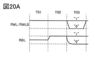
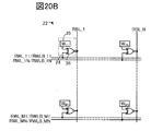
- 20A and 20B are diagrams for explaining a configuration example of the semiconductor device.
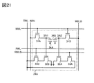
- FIG. 21 is a diagram illustrating a configuration example of a semiconductor device.
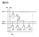
- 22A and 22B are diagrams for explaining a configuration example of the semiconductor device.
- FIG. 23 is a diagram illustrating a configuration example of the semiconductor device.
- FIG. 24 is a diagram illustrating a configuration example of the semiconductor device.
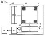
- 25A and 25B are diagrams for explaining a configuration example of the semiconductor device.
- 26A and 26B are diagrams for explaining a configuration example of the semiconductor device.
- 27A and 27B are diagrams illustrating a configuration example of the semiconductor device.
- 28A and 28B are diagrams for explaining a configuration example of the semiconductor device.
- FIG. 21 is a diagram illustrating a configuration example of a semiconductor device.
- 22A and 22B are diagrams for explaining a configuration example of the semiconductor device.
- FIG. 23 is
- FIG. 29 is a diagram illustrating a configuration example of the semiconductor device.
- FIG. 30 is a diagram illustrating a configuration example of a CPU.
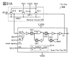
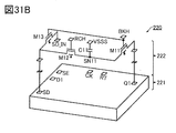
- 31A and 31B are diagrams for explaining a configuration example of a CPU.
- FIG. 32 is a diagram illustrating a configuration example of the CPU.
- FIG. 33 is a diagram illustrating a configuration example of an integrated circuit.
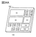
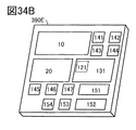
- 34A and 34B are diagrams illustrating a configuration example of an integrated circuit.
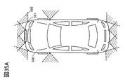
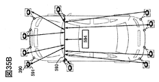
- 35A and 35B are diagrams illustrating application examples of integrated circuits.
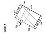
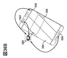
- 36A and 36B are diagrams illustrating application examples of integrated circuits.
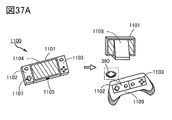
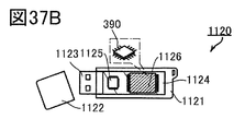
- 37A, 37B and 37C are diagrams illustrating application examples of integrated circuits.
- FIG. 38 is a diagram illustrating an application example of an integrated circuit.
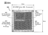
- FIG. 39A is an external photograph of the semiconductor device.
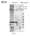
- FIG. 39B is a cross-sectional TEM photograph of the semiconductor device.
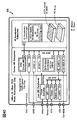
- FIG. 40 is a block diagram illustrating a system configuration of a semiconductor device.
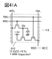
- FIG. 41A is a circuit diagram of a memory cell.
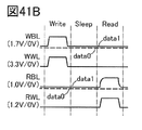
- FIG. 41B is a timing chart showing an operation example of the memory cell.
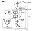
- FIG. 41C is a block diagram showing the configuration of the arithmetic unit.
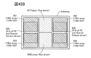
- 42A and 42B are block diagrams illustrating the configuration of the semiconductor device.
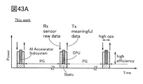
- 43A and 43B are conceptual diagrams illustrating changes in power consumption that occur during the operating period of the semiconductor device.
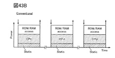
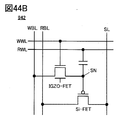
- 44A and 44B are circuit diagrams of an information holding circuit.
- FIG. 45A is a diagram showing an operation waveform after executing the simulation.
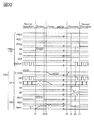
- FIG. 45B is a diagram showing a neural network model assumed in the simulation.
- the ordinal numbers "1st”, “2nd”, and “3rd” are added to avoid confusion of the components. Therefore, the number of components is not limited. Moreover, the order of the components is not limited. Further, for example, the component referred to in “first” in one of the embodiments of the present specification and the like is defined as a component referred to in “second” in another embodiment or in the claims. It is possible. Further, for example, the component referred to in “first” in one of the embodiments of the present specification and the like may be omitted in another embodiment or in the claims.
- the power supply potential VDD may be abbreviated as potentials VDD, VDD, etc. This also applies to other components (eg, signals, voltages, circuits, elements, electrodes, wiring, etc.).
- the code is used for identification such as "_1”, “_2”, “[n]", “[m, n]”. May be added and described.
- the second wiring GL is described as wiring GL [2].
- the semiconductor device refers to all devices that can function by utilizing the semiconductor characteristics.
- a semiconductor device such as a transistor, a semiconductor circuit, an arithmetic unit, and a storage device are one aspect of the semiconductor device.
- a display device liquid crystal display device, light emission display device, etc.
- projection device lighting device, electro-optical device, power storage device, storage device, semiconductor circuit, image pickup device, electronic device, etc. may be said to have a semiconductor device.
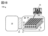
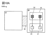
- the semiconductor device 100 includes a CPU 10, an accelerator 20, and a bus 30.
- the accelerator 20 has an arithmetic processing unit 21 and a memory unit 22.
- the arithmetic processing unit 21 has an arithmetic circuit 23.
- the memory unit 22 has a memory circuit 24.
- the memory unit 22 may be referred to as a device memory or a shared memory.
- the memory circuit 24 has a transistor 25 having a semiconductor layer 29 having a channel forming region.
- the arithmetic circuit 23 and the memory circuit 24 are electrically connected via the wiring 31.
- the CPU 10 has a function of performing general-purpose processing such as execution of an operating system, control of data, execution of various operations and programs.
- the CPU 10 has one or more CPU cores.
- Each CPU core has a data holding circuit that can hold data even when the supply of the power supply voltage is stopped.
- the supply of the power supply voltage can be controlled by electrical disconnection from the power supply domain (power domain) by a power switch or the like.
- the power supply voltage may be referred to as a drive voltage.
- a memory having a transistor (OS transistor) having an oxide semiconductor in the channel formation region is suitable.
- the oxide semiconductor is also referred to as a metal oxide.
- the configuration of the CPU core including the data holding circuit including the OS transistor will be described in the fifth embodiment.
- the accelerator 20 has a function of executing a program (also called a kernel or a kernel program) called from a host program.
- the accelerator 20 can perform, for example, parallel processing of matrix operations in graphic processing, parallel processing of product-sum operations of neural networks, parallel processing of floating-point operations in scientific and technological calculations, and the like.
- the memory unit 22 has a function of storing data processed by the accelerator 20. Specifically, it is possible to store data input or output to the arithmetic processing unit 21, such as weight data used for parallel processing of the product-sum operation of the neural network.
- the memory circuit 24 is electrically connected to the arithmetic circuit 23 of the arithmetic processing unit 21 via wiring 31, and has a function of holding a binary or ternary digital value.
- the semiconductor layer 29 included in the transistor 25 is an oxide semiconductor. That is, the transistor 25 is an OS transistor.
- the memory circuit 24 is preferably a memory having an OS transistor (hereinafter, also referred to as an OS memory).
- the OS transistor Since the bandgap of the metal oxide is 2.5 eV or more, the OS transistor has a minimum off current. As an example, voltage 3.5V between the source and the drain, at at room temperature (25 °C), 1 ⁇ less than 10 -20 A state current per channel width 1 [mu] m, less than 1 ⁇ 10 -22 A, or 1 ⁇ 10 It can be less than -24A . That is, the on / off current ratio of the drain current can be set to 20 digits or more and 150 digits or less. Therefore, the OS memory has an extremely small amount of charge leaked from the holding node via the OS transistor. Therefore, since the OS memory can function as a non-volatile memory circuit, power gating of the accelerator becomes possible.
- High-density integrated semiconductor devices may generate heat due to the driving of circuits. Due to this heat generation, the temperature of the transistor rises, which may change the characteristics of the transistor, resulting in a change in field effect mobility and a decrease in operating frequency. Since the OS transistor has higher thermal resistance than the Si transistor, the field effect mobility is less likely to change due to temperature changes, and the operating frequency is less likely to decrease. Further, the OS transistor tends to maintain the characteristic that the drain current increases exponentially with respect to the gate-source voltage even when the temperature rises. Therefore, by using the OS transistor, stable operation can be performed in a high temperature environment.
- the metal oxides applied to the OS transistor are Zn oxide, Zn-Sn oxide, Ga-Sn oxide, In-Ga oxide, In-Zn oxide, and In-M-Zn oxide (M is: Ti, Ga, Y, Zr, La, Ce, Nd, Sn or Hf) and the like.
- M is: Ti, Ga, Y, Zr, La, Ce, Nd, Sn or Hf
- the transistor can be obtained with excellent electrical characteristics such as field effect mobility by adjusting the ratio of the elements.
- oxides containing indium and zinc include aluminum, gallium, yttrium, copper, vanadium, beryllium, boron, silicon, titanium, iron, nickel, germanium, zirconium, molybdenum, lanthanum, cerium, neodymium, hafnium, tantalum, and tungsten. , One or more selected from magnesium and the like may be included.
- the metal oxide applied to the semiconductor layer is preferably a metal oxide having a crystal portion such as CAAC-OS, CAC-OS, and nc-OS.
- CAAC-OS is an abbreviation for c-axis-aligned crystal line oxide semiconductor ductor.
- CAC-OS is an abbreviation for Cloud-Aligned Complex Oxide Semiconductor.
- nc-OS is an abbreviation for nanocrystalline oxide semiconductor.
- CAAC-OS has a c-axis orientation and has a distorted crystal structure in which a plurality of nanocrystals are connected in the ab plane direction.
- the strain refers to a region in which a plurality of nanocrystals are connected in which the orientation of the lattice arrangement changes between a region in which the lattice arrangement is aligned and a region in which another lattice arrangement is aligned.
- the CAC-OS has a function of flowing electrons (or holes) as carriers and a function of not flowing electrons as carriers. By separating the function of flowing electrons and the function of not flowing electrons, both functions can be maximized. That is, by using CAC-OS in the channel formation region of the OS transistor, both a high on-current and an extremely low off-current can be realized.
- OS transistors Since metal oxides have a large bandgap, electrons are less likely to be excited, and the effective mass of holes is large, OS transistors may be less likely to undergo avalanche breakdown than general Si transistors. .. Therefore, for example, hot carrier deterioration caused by avalanche breakdown can be suppressed. By suppressing hot carrier deterioration, the OS transistor can be driven with a high drain voltage.
- the OS transistor is a storage transistor that has a large number of electrons as carriers. Therefore, the influence of DIBL (Drain-Induced Barrier Lowering), which is one of the short-channel effects, is smaller than that of an inverting transistor (typically, a Si transistor) having a pn junction. That is, the OS transistor has higher resistance to the short channel effect than the Si transistor.
- DIBL Drain-Induced Barrier Lowering
- the OS transistor Since the OS transistor has high resistance to the short channel effect, the channel length can be reduced without deteriorating the reliability of the OS transistor. Therefore, the degree of circuit integration can be increased by using the OS transistor.
- the drain electric field becomes stronger as the channel length becomes finer, but as mentioned above, the OS transistor is less likely to undergo avalanche breakdown than the Si transistor.
- the OS transistor has high resistance to the short channel effect, it is possible to make the gate insulating film thicker than the Si transistor. For example, even in a fine transistor having a channel length and a channel width of 50 nm or less, it may be possible to provide a thick gate insulating film of about 10 nm. By thickening the gate insulating film, the parasitic capacitance can be reduced, so that the operating speed of the circuit can be improved. Further, by making the gate insulating film thicker, the leakage current through the gate insulating film is reduced, which leads to a reduction in static current consumption.
- the accelerator 20 can hold data even if the supply of the power supply voltage is stopped by having the memory circuit 24 which is the OS memory. Therefore, the power gating of the accelerator 20 becomes possible, and the power consumption can be significantly reduced.
- the memory circuit 24 composed of the OS transistor can be provided so as to be stacked with the arithmetic circuit 23 that can be configured by Si CMOS. Therefore, the circuit area can be arranged without increasing the circuit area.
- the memory circuit 24 and the arithmetic circuit 23 are electrically connected via a wiring 31 extending in a direction substantially perpendicular to the surface of the substrate on which the arithmetic circuit 23 is provided.
- approximately vertical means a state in which the objects are arranged at an angle of 85 degrees or more and 95 degrees or less.
- the memory circuit 24 can have a NOSRAM circuit configuration.
- NOSRAM registered trademark
- NOSRAM refers to a memory in which the memory cell is a 2-transistor type (2T) or 3-transistor type (3T) gain cell and the access transistor is an OS transistor.
- the OS transistor has an extremely small leakage current, that is, a current flowing between the source and the drain in the off state.
- the NOSRAM can be used as a non-volatile memory by holding the electric charge corresponding to the data in the memory circuit by using the characteristic that the leakage current is extremely small.
- NO SRAM can read the held data without destroying it (non-destructive reading), it is suitable for parallel processing of the product-sum operation of a neural network in which only the data reading operation is repeated in large quantities.
- the arithmetic processing unit 21 has a function of performing arithmetic processing using digital values. Digital values are less susceptible to noise. Therefore, the accelerator 20 is suitable for performing arithmetic processing that requires highly accurate arithmetic results.
- the arithmetic processing unit 21 is preferably composed of Si CMOS, that is, a transistor (Si transistor) having silicon in the channel forming region. With this configuration, it can be provided by stacking with an OS transistor.
- the arithmetic circuit 23 has a function of performing any one of processing such as integer arithmetic, single-precision floating-point arithmetic, and double-precision floating-point arithmetic by using the digital value data held in each of the memory circuits 24 of the memory unit 22. Has.
- the arithmetic circuit 23 has a function of repeatedly executing the same processing such as a product-sum operation.
- the calculation circuit 23 is configured to provide one calculation circuit 23 for each read bit line of the memory circuit 24, that is, for each row (Column) (Column-Parallel Calibration).
- the data for one line of the memory circuit 24 (up to all bit lines) can be arithmetically processed in parallel.
- the data bus size between the CPU and the memory 32 bits, etc.) is not limited. Therefore, in the Colon-Parallel Calction, the degree of parallelism of the calculation can be significantly increased. It is possible to improve the calculation efficiency related to a huge amount of arithmetic processing such as deep neural network learning (deep learning), which is an AI technology, and scientific and technological calculations that perform floating-point arithmetic.
- deep neural network learning deep learning
- the power generated by the memory access (data transfer between the CPU and the memory and the calculation by the CPU) can be reduced, resulting in heat generation and generation. It is possible to suppress an increase in power consumption. Further, by making the physical distance between the arithmetic circuit 23 and the memory circuit 24 close to each other, for example, the wiring distance can be shortened by stacking, the parasitic capacitance generated in the signal line can be reduced, so that the power consumption can be reduced.
- the bus 30 electrically connects the CPU 10 and the accelerator 20. That is, the CPU 10 and the accelerator 20 can transmit data via the bus 30.
- One aspect of the present invention can reduce the size of a semiconductor device that functions as an accelerator for AI technology and the like, which has a huge amount of calculation and a large number of parameters.
- one aspect of the present invention can reduce the power consumption of a semiconductor device that functions as an accelerator for AI technology and the like, which has a huge amount of calculation and a large number of parameters.
- one aspect of the present invention can suppress heat generation in a semiconductor device that functions as an accelerator such as AI technology having a huge amount of calculation and a large number of parameters.
- one aspect of the present invention can reduce the number of data transfers between the CPU and the semiconductor device that functions as a memory in the semiconductor device that functions as an accelerator such as AI technology having a huge amount of calculation and the number of parameters. ..
- semiconductor devices that function as accelerators such as AI technology which has a huge amount of calculation and a large number of parameters, have a non-Von Neumann architecture, and compared to the von Neumann architecture, which consumes more power as the processing speed increases.
- Parallel processing can be performed with extremely low power consumption.
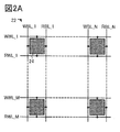
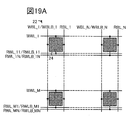
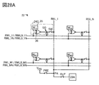
- FIG. 2A is a diagram illustrating a circuit configuration example applicable to the memory unit 22 included in the semiconductor device 100 of the present invention.
- writing word lines WWL_1 to WWL_M are arranged side by side in the matrix direction of M rows and N columns (M and N are natural numbers of 2 or more).
- M and N are natural numbers of 2 or more.
- the read bit lines RBL_1 to RBL_N are shown in the figure.
- the memory circuit 24 connected to each word line and bit line is illustrated.
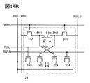
- FIG. 2B is a diagram illustrating a circuit configuration example applicable to the memory circuit 24.
- the memory circuit 24 includes a transistor 25, a transistor 26, a transistor 27, and a capacitance element 28 (also referred to as a capacitor).
- One of the source and drain of the transistor 25 is connected to the writing bit line WBL.
- the gate of the transistor 25 is connected to the writing word line WWL.
- the other of the source or drain of the transistor 25 is connected to one electrode of the capacitive element 28 and the gate of the transistor 26.
- One of the source or drain of the transistor 26 and the other electrode of the capacitive element 28 are connected to a wire that provides a fixed potential, eg, a ground potential.
- the other of the source or drain of the transistor 26 is connected to one of the source or drain of the transistor 27.
- the gate of the transistor 27 is connected to the read word line RWL.
- the other of the source or drain of the transistor 27 is connected to the read bit line RBL.
- the read bit line RBL is connected to the arithmetic circuit 23 via a wiring 31 or the like extending in a direction substantially perpendicular to the surface of the substrate on which the arithmetic circuit 23 is provided.
- the circuit configuration of the memory circuit 24 shown in FIG. 2B corresponds to a NO SRAM of a 3-transistor type (3T) gain cell.
- the transistor 25 to the transistor 27 are OS transistors.
- the OS transistor has an extremely small leakage current, that is, a current flowing between the source and the drain in the off state.
- the NOSRAM can be used as a non-volatile memory by holding the electric charge corresponding to the data in the memory circuit by using the characteristic that the leakage current is extremely small.
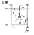
- FIG. 3A is a diagram illustrating an example of a circuit configuration applicable to the arithmetic processing unit 21 included in the semiconductor device 100 of the present invention.
- the arithmetic processing unit 21 has N arithmetic circuits 23_1 to 23_N.
- Each of the N arithmetic circuits 23_1 to 23_N receives a signal of any one of N read bit lines RBL_1 to read bit lines RBL_N, and outputs output signals Q_1 to Q_N.
- the signal of the read bit line RBL_1 to the read bit line RBL_N may be amplified and read by a sense amplifier or the like.
- the output signals Q_1 to Q_N correspond to the data obtained by performing the product-sum operation using the data held in the memory circuit 24.
- FIG. 3B is a diagram illustrating a circuit configuration example of the arithmetic circuit 23 applicable to the arithmetic circuit 23_1 to the arithmetic circuit 23_N.
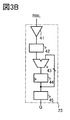
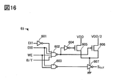
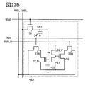
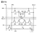
- FIG. 4 is a circuit for executing arithmetic processing based on the architecture of Binary Neural Network (BNN).
- the calculation circuit 23 includes a read circuit 41 to which a signal of the read bit line RBL is given, a bit product sum calculation unit 42, an accumulator 43, a latch circuit 44, and a coding circuit 45 that outputs an output signal Q.
- FIG. 4 shows a configuration example showing more details about the configuration of the arithmetic circuit 23 shown in FIG. 3B.
- the product-sum calculation of 8-bit signals (W [0] to W [7], A [0] to A [7]) is performed, and 1-bit output signal Q and 11-bit output signal (acout) are performed.
- the configuration for outputting [10: 0]) is shown as an example.
- the same product of M pieces and their sum can be executed in 8 parallel ⁇ 1 bit ⁇ M / 8 lines, so that M / 8 clock is required. Therefore, in the configuration of FIG. 4, the calculation time can be shortened by executing the multiply-accumulate operation in parallel, so that the calculation efficiency can be improved.
- the bit product-sum calculator 42 is obtained by an adder to which an 8-bit signal (W [0] to W [7], A [0] to A [7]) is input, and the adder. It has an adder in which the value is input.
- the product of 1-bit signals calculated in 8 parallels is shown as WA0 to WA7, the sum thereof is shown as WA10, WA32, WA54, WA76, and the sum thereof is shown as WA3210, WA7654.
- the accumulator 43 functioning as an adder outputs the sum of the signal of the bit multiply-accumulate calculator 42 and the output signal of the latch circuit 44 to the latch circuit 44.
- the accumulator 43 switches the signal to be input to the adder according to the control signal TxD_EN.
- TxD_EN 0
- the control signal TxD_EN 1
- TxD_EN 1
- the logic circuit 47 composed of the AND circuit is used for batch normalization after the product-sum calculation of the signals A [0] to A [7] and the signals W [0] to W [7] is completed. Add the data together. Specifically, the signals W [7] are added while switching with the switching signal (th select [10: 0]).
- the data for batch normalization may be configured to be simultaneously read and selected from signals W [0] to W [6] other than the signal W [7], for example.
- Batch normalization is an operation for adjusting the distribution of output data of each layer in a neural network so as to be constant. For example, image data often used for calculations in neural networks may differ from the distribution of prediction data (input data) because the distribution of data used for training tends to vary.
- Batch normalization can improve the accuracy of learning in a neural network by normalizing the distribution of input data to the intermediate layer of the neural network to a Gaussian distribution with an average of 0 and a variance of 1.
- BNN Binary Neural Network
- the latch circuit 44 holds the output signal (acout [10: 0]) of the accumulator 43.
- the binary data passed to the layer (NN layer) in the next neural network by batch normalization becomes the most significant bit of the product-sum operation result held by the latch circuit 44.
- the signal of the most significant bit (acout10) represents the sign of the latch data calculated by the two's complement, and the plus data is 1 and the minus data is 0. Since it is passed to the NN layer, it is inverted by the inverter circuit 46 that functions as a coding circuit, and is output as an output signal Q. Since Q is the output of the intermediate layer, it is temporarily held in the buffer memory (also referred to as an input buffer) in the accelerator 20 and then used for the calculation of the next layer.
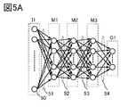
- FIG. 5A illustrates a hierarchical neural network based on the Binary Neural Network (BNN) architecture.
- FIG. 5A illustrates a fully connected neural network of a neuron 50, an input layer 1 layer (I1), an intermediate layer 3 layers (M1 to M3), and an output layer 1 layer (O1).
- the number of neurons in the input layer I1 is 786
- the number of neurons in the intermediate layers M1 to M3 is 256
- the number of neurons in the output layer O1 is 10
- the number of connections in each layer (layer 51, layer 52, layer 53 and layer 54) is ( 784 x 256) + (256 x 256) + (256 x 256) + (256 x 10), for a total of 334,336 pieces. That is, since the weight parameters required for the neural network calculation are about 330 Kbits in total, the memory capacity can be sufficiently implemented even in a small-scale system.
- FIG. 5B shows a detailed block diagram of the semiconductor device 100 capable of calculating the neural network shown in FIG. 5A.
- FIG. 5B in addition to the arithmetic processing unit 21, the arithmetic circuit 23, the memory unit 22, the memory circuit 24, and the wiring 31 described with reference to FIGS. 1A and 1B, each configuration shown in FIGS. 1A and 1B is driven.
- the configuration example of the peripheral circuit of is shown in the figure.
- FIG. 5B illustrates a controller 61, a row decoder 62, a word line driver 63, a column decoder 64, a write driver 65, a precharge circuit 66, a sense amplifier 67, a selector 68, an input buffer 71, and an arithmetic control circuit 72.
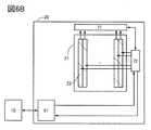
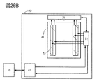
- FIG. 6A is a diagram in which blocks for controlling the memory unit 22 are extracted for each configuration shown in FIG. 5B.
- the controller 61, the row decoder 62, the word line driver 63, the column decoder 64, the write driver 65, the precharge circuit 66, the sense amplifier 67, and the selector 68 are extracted and shown.
- the controller 61 processes an input signal from the outside to generate a control signal for the row decoder 62 and the column decoder 64.
- the input signal from the outside is a control signal for controlling the memory unit 22 such as a write enable signal and a read enable signal. Further, the controller 61 inputs / outputs data written to the memory unit 22 or data read from the memory unit 22 via a bus with the CPU 10.
- the low decoder 62 generates a signal for driving the word line driver 63.
- the word line driver 63 generates a signal to be given to the writing word line WWL and the reading word line RWL.
- the column decoder 64 generates a signal for driving the sense amplifier 67 and the write driver 65.
- the sense amplifier 67 amplifies the potential of the read bit line RBL.
- the write driver generates a signal for controlling the read bit line RBL and the write bit line WBL.
- the precharge circuit 66 has a function of precharging a read bit line RBL or the like.
- the signal read from the memory circuit 24 of the memory unit 22 is input to the arithmetic circuit 23 and can be output via the selector 68.
- the selector 68 can sequentially read data corresponding to the bus width and output necessary data to the CPU 10 or the like via the controller 61.
- FIG. 6B is a diagram in which blocks for controlling the arithmetic processing unit 21 are extracted for each configuration shown in FIG. 5B.
- the controller 61 processes the input signal from the outside to generate the control signal of the arithmetic control circuit 72. Further, the controller 61 generates various signals for controlling the arithmetic circuit 23 included in the arithmetic processing unit 21. Further, the controller 61 inputs / outputs data related to the calculation result via the input buffer 71. By using the input buffer 71, parallel calculation of the number of bits equal to or larger than the data bus width of the CPU becomes possible. Further, since the number of times that a huge number of weight parameters are transferred to and from the CPU 10 can be reduced, power consumption can be reduced.
- One aspect of the present invention can reduce the size of a semiconductor device that functions as an accelerator for AI technology and the like, which has a huge amount of calculation and a large number of parameters.
- one aspect of the present invention can reduce the power consumption of a semiconductor device that functions as an accelerator for AI technology and the like, which has a huge amount of calculation and a large number of parameters.
- one aspect of the present invention can suppress heat generation in a semiconductor device that functions as an accelerator such as AI technology having a huge amount of calculation and a large number of parameters.
- one aspect of the present invention can reduce the number of data transfers between the CPU and the semiconductor device that functions as a memory in the semiconductor device that functions as an accelerator such as AI technology having a huge amount of calculation and the number of parameters. ..
- semiconductor devices that function as accelerators such as AI technology which has a huge amount of calculation and a large number of parameters, have a non-Von Neumann architecture, and compared to the von Neumann architecture, which consumes more power as the processing speed increases.
- Parallel processing can be performed with extremely low power consumption.
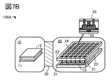
- FIGS. 7A and 7B are diagrams for explaining the semiconductor device 100A, which is one aspect of the present invention.
- the CPU 10 has a CPU core 11 and a backup circuit 12.
- the accelerator 20 has an arithmetic processing unit 21 and a memory unit 22.
- the arithmetic processing unit 21 has a drive circuit 15 and an arithmetic circuit 23.
- the drive circuit 15 is a circuit for driving the memory unit 22.
- the memory unit 22 has a memory circuit 24.
- the memory unit 22 may be referred to as a device memory or a shared memory.
- the memory circuit 24 has a transistor 25 having a semiconductor layer 29 having a channel forming region.
- the drive circuit 15 and the memory circuit 24 are electrically connected via the wiring 31.
- the memory circuit 24 is electrically connected to the arithmetic circuit 23 of the arithmetic processing unit 21 via the wiring 31 and the drive circuit 15.
- the memory circuit 24 has a function of holding binary or ternary data as an analog voltage value.
- the arithmetic processing unit 21 can efficiently perform arithmetic processing based on architectures such as Binary Neural Network (BNN) and Ternary Neural Network (TNN).
- BNN Binary Neural Network
- TNN Ternary Neural Network
- the drive circuit 15 has a write circuit for writing data to the memory unit 22 and a read circuit for reading data from the memory unit 22.
- the write circuit binary or 3 values data to be written to the memory circuit 24 in the memory unit 22 according to various signals such as a switching signal for switching the writing of the binary or trivalent data signal, a write control signal, and a data signal. It has a function to switch to the voltage value and output it.
- the writing circuit is composed of a logic circuit in which a plurality of signals are input.
- the read circuit has a function of switching the voltage value held in the memory circuit 24 in the memory unit 22 into a binary or ternary data signal and reading the data using a plurality of reference voltages.
- the readout circuit has the function of a sense amplifier.
- the memory circuit 24 and the drive circuit 15 composed of OS transistors are electrically connected via wiring 31 extending in a direction substantially perpendicular to the surface of the substrate on which the drive circuit 15 and the arithmetic circuit 23 are provided. Be connected.
- the term "approximately vertical" means a state in which the objects are arranged at an angle of 85 degrees or more and 95 degrees or less.
- the bit lines connected to the memory circuit 24 are the write bit line and the read bit line, it is preferable that they are connected via separate wirings.
- the write bit line is connected to the write circuit via wiring (first wiring) provided substantially perpendicular to the surface of the substrate on which the drive circuit 15 and the arithmetic circuit 23 are provided.
- the read bit line is connected to the read circuit via a wiring (second wiring) provided substantially perpendicular to the surface of the substrate on which the drive circuit 15 and the arithmetic circuit 23 are provided.
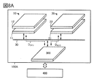
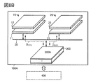
- FIG. 8A in addition to the configuration of the semiconductor device 100A described with reference to FIGS. 7A and 7B, the OS memory 300 connected to the bus 30 and the main memory 400 composed of a DRAM or the like are shown. Further, in FIG. 8A, the data between the OS memory 300 and the CPU 10 is shown as a data D CPU . Further, in FIG. 8A, the data between the OS memory 300 and the accelerator 20 is illustrated as data D ACC .
- the accelerator 20 can continue to hold the binary or ternary analog voltage value as data, and the CPU 10 calculates the calculation result obtained by the calculation circuit. It can be configured to output to. Therefore, the data D ACC from the OS memory 300 for arithmetic processing can be reduced. Further, since the amount of arithmetic processing of the CPU 10 can be reduced, the data D CPU between the OS memory 300 and the CPU 10 can also be reduced. That is, in the configuration of one aspect of the present invention, it is possible to reduce the number of accesses via the bus 30 and the amount of data to be transferred.
- the backup circuit 12 in the CPU 10 and the memory unit 22 in the accelerator 20 can be provided so as to be stacked with the CPU core 11 and the arithmetic processing unit 21 which can be configured by Si CMOS. Therefore, the circuit area can be arranged without increasing the circuit area.
- DOSRAM is an abbreviation for "Dynamic Oxide Semiconductor Random Access Memory (RAM)" and refers to a RAM having a 1T (transistor) 1C (capacity) type memory cell.
- RAM Dynamic Oxide Semiconductor Random Access Memory
- DOSRAM is a memory that utilizes the low off-current of the OS transistor.
- the DOSRAM is a DRAM formed by using an OS transistor, and the DOSRAM is a memory that temporarily stores information sent from the outside.
- the DOSRAM has a memory cell including an OS transistor and a read circuit unit including a Si transistor (a transistor having silicon in a channel forming region). Since the memory cell and the read circuit unit can be provided in different stacked layers, the overall circuit area of the DOSRAM can be reduced. In addition, the DOSRAM can divide the memory cell array into small pieces and arrange them efficiently.
- the OS memory 300 is formed by stacking layers having OS transistors to form an OS memory 300N in which DOSRAM is highly integrated, thereby increasing the storage capacity per unit area. Can be made larger. In this case, it is possible to omit the main memory 400 provided separately from the semiconductor device 100A.
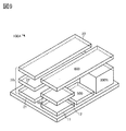
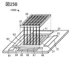
- FIG. 9 shows a schematic diagram of a semiconductor device 100A that functions as a SoC in which a CPU 10, an accelerator 20, and an OS memory 300N are tightly coupled.
- the backup circuit 12 can be provided in the layer having the OS transistor on the upper layer of the CPU core 11.
- the memory unit 22 can be provided on the layer having the OS transistor on the upper layer of the arithmetic processing unit 21.
- the stacked OS memory 300N can be arranged in the same manner as the memory unit 22.
- a control circuit 500 having a Si transistor, a logic circuit 600 having an OS transistor, and the like can be provided.
- the logic circuit 600 is preferably a simple logic circuit such as a changeover switch that can be replaced with an OS transistor.
- the OS transistor has a fluctuation amount of electrical characteristics due to heat as compared with the Si transistor. It is suitable because it is small. Further, by integrating the circuits in the three-dimensional direction as shown in FIG. 9, the parasitic capacitance can be reduced as compared with a laminated structure using a through silicon via (Through Silicon Via: TSV) or the like. .. It is possible to reduce the power consumption required for charging and discharging each wiring. Therefore, it is possible to improve the calculation processing efficiency.
- TSV Through Silicon Via
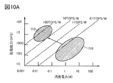
- FIG. 10A is a diagram for explaining the relationship between the processing performance (OPS: Operations Per Second) and the power consumption (W).
- OPS Operations Per Second
- W power consumption
- the vertical axis represents the processing capacity
- the horizontal axis represents the power consumption.
- 0.1 TOPS / W Trip Operations Per Second / W
- 1 TOPA / W 1 TOPA / W
- 10 TOPS / W and 100 TOPS / W are clearly indicated by broken lines as indexes of calculation efficiency. ..
- the region 710 shows the region including the conventional general-purpose AI accelerator (Von Neumann type), and the region 712 shows the region including the semiconductor device of one aspect of the present invention.
- the area 710 includes, for example, a CPU (Central Processing Unit), a GPU (Graphics Processing Unit), an FPGA (Field-Programmable Gate Array), and the like.
- the semiconductor device of one aspect of the present invention by applying the semiconductor device of one aspect of the present invention, it is possible to reduce the power consumption by about two orders of magnitude and improve the processing performance as compared with the conventional general-purpose AI accelerator (Von Neumann type). It can be significantly improved (for example, 1000 times or more). By applying the semiconductor device of one aspect of the present invention, a calculation efficiency of 100 TOPS / W or more can be expected.
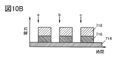
- FIG. 10B shows an image diagram of the power consumption of the semiconductor device having the conventional configuration in image recognition
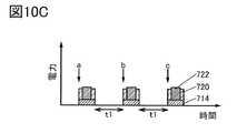
- FIG. 10C shows an image diagram of the power consumption of the semiconductor device using the configuration of one aspect of the present invention in image recognition.
- the vertical axis represents electric power and the horizontal axis represents time.
- the electric power 714 indicates the leak power
- the electric power 716 indicates the CPU power
- the electric power 718 indicates the memory power.
- the electric power 714 indicates the leak power
- the electric power 720 indicates the CPU power
- the electric power 722 indicates the accelerator power.
- the electric power 722 also includes the electric power used for the arithmetic circuit and the memory circuit.
- the arrows a, b, and c represent signals in image recognition, respectively. It is assumed that the semiconductor device starts arithmetic processing such as image recognition when the signals of the arrows a, b, and c are input.
- a constant leakage power (power 714) is generated with respect to time.
- the leakage power (electric power) while using the CPU power (electric power 720) and the accelerator power (electric power 722). 714) is generated, but during the period when the CPU power (power 720) and the accelerator power (power 722) are not used, the leak power (power 714) does not occur during the normally-off drive (the period shown in FIG. 10C). It can be t1). This makes it possible to significantly reduce power consumption. That is, it is possible to provide a semiconductor device having extremely low power consumption.
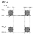
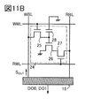
- FIG. 11A is a diagram illustrating an example of a circuit configuration applicable to the memory unit 22 included in the semiconductor device 100A of the present invention.
- writing word lines WWL_1 to WWL_M writing word lines RWL_1 to RWL_M, writing bit lines WBL_1 WBL_N, and writing word lines WWL_1 to WWL_M arranged side by side in the matrix direction of M rows and N columns (M and N are natural numbers of 2 or more), and
- M and N are natural numbers of 2 or more
- the read bit lines RBL_1 to RBL_N are shown in the figure.
- the memory circuit 24 connected to each word line and bit line is illustrated.
- FIG. 11B is a diagram illustrating a circuit configuration example applicable to the memory circuit 24.
- the memory circuit 24 includes a transistor 25, a transistor 26, a transistor 27, and a capacitance element 28 (also referred to as a capacitor).
- One of the source and drain of the transistor 25 is connected to the writing bit line WBL.
- the gate of the transistor 25 is connected to the writing word line WWL.
- the other of the source or drain of the transistor 25 is connected to one electrode of the capacitive element 28 and the gate of the transistor 26.
- One of the source or drain of the transistor 26 and the other electrode of the capacitive element 28 are connected to a wire that provides a fixed potential, eg, a ground potential.
- the other of the source or drain of the transistor 26 is connected to one of the source or drain of the transistor 27.
- the gate of the transistor 27 is connected to the read word line RWL.
- the other of the source or drain of the transistor 27 is connected to the read bit line RBL.
- the write bit line WBL and the read bit line RBL are connected to the drive circuit 15 via wiring or the like extending in a direction substantially perpendicular to the surface of the substrate on which the arithmetic circuit 23 is provided. Be connected.
- the drive circuit 15 outputs a data signal S OUT which is a binary or ternary analog voltage value. Further, the drive circuit 15 is given a voltage of the read bit line RBL corresponding to the data read from the memory circuit 24, and outputs data signals DO0 and DO1 corresponding to the voltage.
- the circuit configuration of the memory circuit 24 shown in FIG. 11B corresponds to a NO SRAM of a 3-transistor type (3T) gain cell.
- the transistor 25 to the transistor 27 are OS transistors.
- the OS transistor has an extremely small leakage current, that is, a current flowing between the source and the drain in the off state.
- the NOSRAM can be used as a non-volatile memory by holding the electric charge corresponding to the data in the memory circuit by using the characteristic that the leakage current is extremely small.
- each transistor may have a back gate. By having a back gate, it is possible to improve the transistor characteristics.
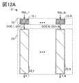
- FIG. 12A is a diagram illustrating an example of a circuit configuration applicable to the arithmetic processing unit 21 included in the semiconductor device 100A of the present invention.
- the arithmetic processing unit 21 has a drive circuit 15 and an arithmetic circuit 23.
- the drive circuit 15 has N drive circuits 15_1 to 15_N.
- the arithmetic circuit 23 has N arithmetic circuits 23_1 to 23_N.
- a signal of any one of N read bit lines RBL_1 to read bit line RBL_N is input to each of the N drive circuits 15_1 to 15_N, and the data signals DO0_1 to DO0_N and / or the data signals DO1_1 to DO1_N are input. Is output.
- the data signals DO0_1 to DO0_N and / or the data signals DO1_1 to DO1_N are input to the arithmetic circuits 23_1 to 23_N to obtain output signals Y_1 to Y_N.
- the output signals Y_1 to Y_N correspond to the data obtained by performing the product-sum operation using the data held in the memory circuit 24.
- FIG. 12B is a diagram illustrating a circuit configuration example of the arithmetic circuit 23 applicable to the arithmetic circuit 23_1 to the arithmetic circuit 23_N.
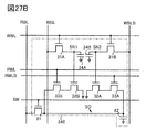
- FIG. 13 is a circuit for executing arithmetic processing based on the architecture of Binary Neural Network (BNN) or Ternary Neural Network (TNN).
- the calculation circuit 23 includes a read circuit 41 to which the data signal DO0 and / or the data signal DO1 is input, a bit product / sum calculation unit 42, an accumulator 43, a latch circuit 44, and a coding circuit 45 to output the output signal Y. Have.
- FIG. 13 shows a configuration example showing more details about the configuration of the arithmetic circuit 23 shown in FIG. 12B.
- the product-sum calculation of 8-bit signals (W [0] to W [7], A [0] to A [7]) is performed, and the output signal Y and the 11-bit output signal (acout [10:: The configuration for outputting 0]) is shown as an example.
- the same product of M pieces and their sum can be executed in 8 parallel ⁇ 1 bit ⁇ M / 8 lines, so that M / 8 clock is required. Therefore, in the configuration of FIG. 13, the calculation time can be shortened by executing the multiply-accumulate operation in parallel, so that the calculation efficiency can be improved.
- bit product-sum calculator 42 is obtained by an adder to which an 8-bit signal (W [0] to W [7], A [0] to A [7]) is input and the adder. It has an adder in which the value is input.
- the product of 1-bit signals calculated in 8 parallels is shown as WA0 to WA7, the sum thereof is shown as WA10, WA32, WA54, WA76, and the sum thereof is shown as WA3210, WA7654.
- the accumulator 43 functioning as an adder outputs the sum of the signal of the bit multiply-accumulate calculator 42 and the output signal of the latch circuit 44 to the latch circuit 44.
- the accumulator 43 switches the signal to be input to the adder according to the control signal TxD_EN.
- TxD_EN 0
- the control signal TxD_EN 1
- TxD_EN 1
- the logic circuit 47 composed of the AND circuit is used for batch normalization after the product-sum calculation of the signals A [0] to A [7] and the signals W [0] to W [7] is completed.
- the signal W [7] is added while switching with the data, specifically, the switching signal (th select [10: 0]).
- the data for batch normalization may be configured to be simultaneously read and selected from signals W [0] to W [6] other than the signal W [7], for example.
- Batch normalization is an operation for adjusting the distribution of output data of each layer in a neural network so as to be constant. For example, image data often used for calculations in neural networks may differ from the distribution of prediction data (input data) because the distribution of data used for training tends to vary.
- Batch normalization can improve the accuracy of learning in a neural network by normalizing the distribution of input data to the intermediate layer of the neural network to a Gaussian distribution with an average of 0 and a variance of 1.
- BNN Binary Neural Network
- the latch circuit 44 holds the output signal (acout [10: 0]) of the accumulator 43.
- the binary data passed to the layer (NN layer) in the next neural network by batch normalization becomes the most significant bit of the product-sum operation result held by the latch circuit 44.
- the signal of the most significant bit (acout10) represents the sign of the latch data calculated by the two's complement, and the plus data is 1 and the minus data is 0. Since it is passed to the NN layer, it is inverted by the inverter circuit 46 that functions as a coding circuit, and is output as an output signal Y. Since Y is the output of the intermediate layer, it is temporarily stored in the buffer memory (also referred to as an input buffer) in the accelerator 20 and then used for the calculation of the next layer.
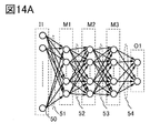
- FIG. 14A illustrates a hierarchical neural network based on the architecture of Binary Neural Network (BNN) or Ternary Neural Network (TNN).
- FIG. 14A illustrates a fully connected neural network of a neuron 50, an input layer 1 layer (I1), an intermediate layer 3 layers (M1 to M3), and an output layer 1 layer (O1). Assuming that the number of neurons in the input layer I1 is 786, the number of neurons in the intermediate layers M1 to M3 is 256, and the number of neurons in the output layer O1 is 10, for example, in Binary Neural Network (BNN), each layer (layer 51, layer 52, layer 53).
- BNN Binary Neural Network
- the number of bonds of the layer 54 is (784 ⁇ 256) + (256 ⁇ 256) + (256 ⁇ 256) + (256 ⁇ 10), for a total of 334336. That is, since the weight parameters required for the neural network calculation are about 330 Kbits in total, the memory capacity can be sufficiently implemented even in a small-scale system.
- FIG. 14B shows a detailed block diagram of the semiconductor device 100A capable of calculating the neural network shown in FIG. 14A.
- FIG. 14B in addition to the arithmetic processing unit 21, the arithmetic circuit 23, the memory unit 22, the memory circuit 24, and the wiring 31 described with reference to FIGS. 7A and 7B, each configuration shown in FIGS. 7A and 7B is driven.
- the configuration example of the peripheral circuit of is shown in the figure.
- FIG. 14B illustrates the controller 61, the row decoder 62, the word line driver 63, the column decoder 64, the write driver 65, the precharge circuit 66, the sense amplifier 67, the selector 68, the input buffer 71, and the arithmetic control circuit 72.
- FIG. 15A is a diagram in which blocks for controlling the memory unit 22 are extracted for each configuration shown in FIG. 14B.
- the controller 61, the row decoder 62, the word line driver 63, the column decoder 64, the write driver 65, the precharge circuit 66, the sense amplifier 67, and the selector 68 are extracted and shown.
- the drive circuit 15 illustrated in FIGS. 7A and 7B corresponds to a block of a write driver 65, a precharge circuit 66, and a sense amplifier 67.
- the drive circuit 15 may include a word line driver 63 and a column decoder 64.
- the controller 61 processes an input signal from the outside to generate a control signal for the row decoder 62 and the column decoder 64.
- the input signal from the outside is a control signal for controlling the memory unit 22 such as a write enable signal and a read enable signal. Further, the controller 61 inputs / outputs data written to the memory unit 22 or data read from the memory unit 22 via a bus with the CPU 10.
- the low decoder 62 generates a signal for driving the word line driver 63.
- the word line driver 63 generates a signal to be given to the write word line WWL and the read word line RWL.
- the column decoder 64 generates a signal for driving the sense amplifier 67 and the write driver 65.
- the precharge circuit 66 has a function of precharging a read bit line RBL or the like.
- the signal read from the memory circuit 24 of the memory unit 22 is input to the arithmetic circuit 23 and can be output via the selector 68.
- the selector 68 can sequentially read the data corresponding to the bus width and output the necessary data to the CPU 10 or the like via the controller 61.
- FIG. 15B is a diagram in which blocks for controlling the arithmetic processing unit 21 are extracted for each configuration shown in FIG. 14B.
- the controller 61 processes the input signal from the outside to generate the control signal of the arithmetic control circuit 72. Further, the controller 61 generates various signals for controlling the arithmetic circuit 23 included in the arithmetic processing unit 21. Further, the controller 61 inputs / outputs data related to the calculation result via the input buffer 71. By using this buffer memory, parallel calculation of the number of bits larger than the data bus width of the CPU becomes possible. Further, since the number of times that a huge number of weight parameters are transferred to and from the CPU 10 can be reduced, power consumption can be reduced.
- FIG. 16 describes a configuration example of a write driver 65 for writing a data signal converted into a binary or ternary analog voltage value to a memory circuit.
- the write driver 65 includes an inverter circuit 601 and a NAND circuit 602, a NAND circuit 603, an inverter circuit 604, a transistor 605, a transistor 606, and an inverter circuit 607.
- the transistor constituting the write driver 65 is a Si transistor.
- One of the source or drain of the transistor 605 and the transistor 606 is given the potential VDD (> GND) or the potential VDD / 2 (> GND) as shown in FIG. Further, a data signal DI1 which is input data is given to the inverter circuit 601.
- the data signal DI0, the write control signal WE for controlling the writing of data, and the switching signal B / for switching the writing of the binary or ternary data signal. T is input.
- the data signal DI0 and the write control signal WE are input to the NAND circuit 603.
- the inverter circuit 607 outputs a data signal S OUT corresponding to a voltage value corresponding to binary or ternary data.
- the data signal S OUT is switched to voltage VDD or voltage GND according to the data signal DI0.
- the data signal S OUT is switched to the three values of voltage VDD, voltage VDD / 2 or voltage GND according to the data signals DI0 and DI1.
- the switched voltage can be written to the memory circuit via the write bit line WBL.
- FIG. 17 describes a configuration example including a sense amplifier 67 that outputs a data signal corresponding to a binary or ternary analog voltage value to the arithmetic circuit 23.
- the comparison circuit 611 and the comparison circuit 612 which generate the data signals DO0 and DO1 which are the output data from the potential of the read bit line RBL corresponding to the input signal, function as the sense amplifier 67.
- the comparison circuit 611 is given the potential of the read bit line RBL potential and the reference voltage Vref1.
- the comparison circuit 612 is given the potential of the read bit line RBL potential and the reference voltage Vref2.
- the reference voltage Vref2 is larger than the reference voltage Vref1 and smaller than VDD.
- the reference voltage Vref1 is greater than GND and less than VDD / 2.
- the data signal DO0 and the data signal BO which are binary output data output via the buffer circuit 613, are obtained.
- the data signal DO0 has the same logical value as the data signal BO.
- the truth table of each signal of the data signal DO0 and the data signal BO is as shown in Table 2.
- the data signal Y output via the arithmetic circuit 23 is obtained.
- the truth table of each signal of the data signal DO0, the data signal DO1 and the data signal Y is as shown in Table 3.
- one aspect of the present invention can provide a miniaturized semiconductor device in a semiconductor device including an accelerator and a CPU.
- one aspect of the present invention can provide a semiconductor device having reduced power consumption in a semiconductor device including an accelerator and a CPU.
- one aspect of the present invention can provide a semiconductor device in which heat generation is suppressed in a semiconductor device including an accelerator and a CPU.
- one aspect of the present invention can provide a semiconductor device in which the number of data transfers in the CPU is reduced.
- a semiconductor device having a new configuration can be provided.
- the semiconductor device of one aspect of the present invention has a non-Von Neumann architecture and performs parallel processing with extremely low power consumption as compared with the von Neumann architecture in which the power consumption increases as the processing speed increases. It can be carried out.
- the semiconductor device 100B includes a CPU 10, an accelerator 20, and a bus 30.
- the accelerator 20 has an arithmetic processing unit 21 and a memory unit 22.
- the arithmetic processing unit 21 has an arithmetic circuit 23.
- the memory unit 22 has a memory circuit 24.
- the memory unit 22 may be referred to as a device memory or a shared memory.
- the memory circuit 24 has a transistor 25 having a semiconductor layer 29 having a channel forming region.
- the arithmetic circuit 23 and the memory circuit 24 are electrically connected via the wiring 31.
- the memory unit 22 has a function of storing and generating data processed by the accelerator 20. Specifically, it has a function of storing weight data (also referred to as a first data signal) used for parallel processing of a product-sum operation of a neural network. Further, the memory unit 22 has a function of generating output data (third data signal) according to the result of multiplication with input data (also referred to as a second data signal). The memory unit has a function of inputting the generated output data to the arithmetic processing unit 21.
- the memory circuit 24 is electrically connected to the arithmetic circuit 23 of the arithmetic processing unit 21 via wiring 31, and has a function of holding weight data represented by two values, that is, a 1-bit digital signal. Further, the memory circuit has a function of generating a signal obtained by exclusive OR corresponding to the multiplication result of the weight data and the input data.
- the semiconductor layer 29 included in the transistor 25 is an oxide semiconductor. That is, the transistor 25 is an OS transistor.
- the memory circuit 24 is preferably a memory having an OS transistor (hereinafter, also referred to as an OS memory).
- FIG. 19A is a diagram illustrating an example of a circuit configuration applicable to the memory unit 22 included in the semiconductor device 100B of the present invention.
- writing word lines WWL_1 to WWL_M writing word lines WWL_11 to RWL_MN, reading word lines RWL_11 to RWL_MN, and reading inverted word lines RWLB_11 to RWLB_MN are arranged side by side in the matrix direction of M rows and N columns (M and N are natural numbers of 2 or more).
- M and N are natural numbers of 2 or more.
- the writing bit line WBL_1 WBL_N, the writing inversion bit line WBLB_1 WBLB_N, and the reading bit lines RBL_1 to RBL_N are shown in the figure. Further, a plurality of memory circuits 24 connected to each word line and bit line are illustrated.
- FIG. 19B is a diagram illustrating a circuit configuration example applicable to the memory circuit 24.
- the memory circuit 24 includes transistors 31A and 31B, transistors 32A and 32B, transistors 33A and 33B, and capacitive elements 34A and 34B (also referred to as capacitors).
- each element includes a writing word line WWL, a reading word line RWL, a reading inverted word line RWLB, a writing bit line WBL, a writing inverted bit line WBLB, and a reading. It is connected to each wiring of the bit wire RBL.
- One electrode of the capacitive elements 34A and 34B and one of the source or drain of the transistors 32A and 32B are connected to a wiring that gives a fixed potential, for example, a ground potential.
- the read bit line RBL is connected to the arithmetic circuit 23 via a wiring 31 or the like extending in a direction substantially perpendicular to the surface of the substrate on which the arithmetic circuit 23 is provided.
- the circuit configuration of the memory circuit 24 shown in FIG. 19B is a transistor 31A, a transistor 32A, a transistor 33A, and a transistor 31B, a transistor 32B, and a transistor 33B, which constitute a NO SRAM of a 3-transistor type (3T) gain cell.
- the transistors 31A and 31B, the transistors 32A and 32B, and the transistors 33A and 33B are OS transistors.
- the OS transistor has an extremely small leakage current, that is, a current flowing between the source and the drain in the off state.
- the NOSRAM can be used as a non-volatile memory by holding the electric charge corresponding to the data in the memory circuit by using the characteristic that the leakage current is extremely small.
- the electric charge given to the nodes SN1 and SN2 can be retained.
- Each transistor may have a back gate electrode.
- the truth table of the memory circuit 24 in FIG. 19B is as shown in Table 4.
- Table 3 the H level and L level voltages are represented by logics "1" and "0".
- “RWL” and “RWLB” correspond to the logic corresponding to the voltage of the read word line RWL and the read inverted word line RWLB given as input data.
- “SN1” and “SN2” correspond to the logic corresponding to the voltage given to the nodes SN1 and SN2 from the writing bit line WBL and the writing inversion bit line WBLB as weight data.
- “RBL” corresponds to the logic corresponding to the voltage of the read bit line RBL generated as output data.
- the read word line RWL, the read inverted word line RWLB are set to the H level, and the read bit line RBL is set to the intermediate potential.
- the read word line RWL and the read inverted word line RWLB are set to H level, and the read bit line RBL is set to H level to be electrically floated.
- the logic of the read bit line RBL is set to "1" or "0" by setting the read word line RWL and the read inverted word line RWLB to the logics "1" and "0" according to the input data.
- Output data can be generated by changing to "0".
- the memory unit 22 capable of holding the weight data and generating a signal based on the exclusive OR with the input data can be configured as shown in FIG. 20B. That is, in the plurality of memory circuits 24, the weight data W 11 to W MN are held in the storage unit 35, and the input data is exclusively ORed via the read word line RWL_11 to RWL_MN and the read inverted word line RWLB_11 to RWLB_MN. By giving to the sum part 36 (ExOR), the output data based on the exclusive OR of the weight data and the input data can be input to the read bit lines RBL_1 to RBL_N.
- the memory circuit 24 of FIG. 19B can be transformed into the circuit configuration of FIG. 21.
- the memory circuit 24A of FIG. 21 corresponds to a configuration in which the connection of the gates of the transistors 32A and 32B to which the nodes SN1 and SN2 are connected is changed.
- the data of the truth table shown in Table 6 can be obtained.
- the memory circuit 24B of FIG. 22A corresponds to a configuration in which the transistor to which the node SN1 is connected is changed from a transistor having the same polarity to transistors 32_P and 32_N which are a combination of p-channel type and n-channel type.
- transistors 32_P and 32_N Si transistors and the like can be used. With this configuration, the transistor and wiring connected to the node SN2 in FIG. 19B can be omitted.
- the data of the truth table shown in Table 7 can be obtained.
- the memory circuit 24C of FIG. 22B changes the transistors of the same polarity to which the nodes SN1 and SN2 of FIG. 19B are connected to transistors of different polarities 32_P and 32_N, and further adds transistors 37 and 38 and the capacitive element 39. Corresponds to the added configuration. With this configuration, the transistors and wiring connected to the node SN2 can be omitted.
- the truth table of the circuit configuration of FIG. 22B is the same as that of Table 7.
- FIG. 23 is a schematic diagram illustrating a memory unit 22 having a plurality of memory circuits 24 and an arithmetic circuit 23 in the semiconductor device 100B of the present invention.
- the memory circuit 24 in the memory unit 22 includes a storage unit 35 and a multiplication unit 40, respectively.
- Weight data W 1 to W k (k is a natural number of 2 or more) are stored in the storage unit 35, read word line RWL, the input data A 1 to A k is input via the readout inverted word line RWLB multiplication
- An output signal (Y k Ak ⁇ W k ), which is a 1-bit digital signal corresponding to the above, is given to the arithmetic circuit 23.
- each transistor of the memory unit 22 is an OS transistor because it can be provided so as to be laminated with the arithmetic circuit 23.
- the arithmetic circuit 23 shown in FIG. 23 includes an accumulator 49 and a coding circuit 45.
- the calculation circuit 23 can generate the product-sum calculation signal Q by adding the multiplied output signals.
- FIG. 24 shows a configuration example showing more details about the configuration of the arithmetic circuit 23 shown in FIG. 23.
- FIG. 24 is an example of a configuration in which 8-bit signals (WA [0] to WA [7]) are added and a 1-bit output signal Q and an 11-bit output signal (acout [10: 0]) are output. It is illustrated as.
- a configuration in which a product-sum operation and a sum operation for batch normalization are switched is shown.
- the same product of M pieces and their sum can be executed in 8 parallel ⁇ 1 bit ⁇ M / 8 lines, so that M / 8 clock is required. Therefore, in the configuration of FIG. 24, the calculation time can be shortened by executing the product-sum calculation in parallel, so that the calculation efficiency can be improved.
- bit adder 42A has an adder to which an 8-bit signal (WA [0] to WA [7]) is input. As shown in FIG. 24, the sum of the 1-bit signals is shown as WA10, WA32, WA54, WA76, and the sum is shown as WA3210, WA7654.
- the accumulator 49 functioning as an adder outputs the sum of the signal of the bit adder 42A and the output signal of the latch circuit 44 to the latch circuit 44.
- the signal input to the accumulator 49 includes a selector 48 that can be switched according to the control signal TxD_EN.
- TxD_EN 0
- the control signal TxD_EN 1
- TxD_EN 1
- the selector 48 can switch between the product-sum operation and the sum operation for batch normalization.
- the logic circuit 47 composed of the AND circuit has data for batch normalization, specifically, a switching signal (thselect [10: 0]) after the product-sum calculation of the signals WA0 to WA7 is completed.
- the signal RBL_th [10: 0] is added while switching with.
- the signal RBL_th [10: 0] corresponds to the weight data held in the memory circuit 24.
- Batch normalization is an operation for adjusting the distribution of output data of each layer in a neural network so as to be constant. For example, image data often used for calculations in neural networks may differ from the distribution of prediction data (input data) because the distribution of data used for training tends to vary.
- Batch normalization can improve the accuracy of learning in a neural network by normalizing the distribution of input data to the intermediate layer of the neural network to a Gaussian distribution with an average of 0 and a variance of 1.
- BNN Binary Neural Network
- the latch circuit 44 holds the output signal (acout [10: 0]) of the accumulator 49.
- the latch circuit 44 is reset by the signal CLRn.
- the binary data passed to the layer (NN layer) in the next neural network by batch normalization becomes the most significant bit of the product-sum operation result held by the latch circuit 44.
- the signal of the most significant bit (acout10) represents the sign of the latch data calculated by the two's complement, and the plus data is 1 and the minus data is 0. Since it is passed to the NN layer, it is inverted by the inverter circuit 46 that functions as a coding circuit, and is output as an output signal Q. Since Q is the output of the intermediate layer, it is temporarily held in the buffer memory (also referred to as an input buffer) in the accelerator 20 and then used for the calculation of the next layer.
- FIG. 25A illustrates a hierarchical neural network based on the Binary Neural Network (BNN) architecture.
- FIG. 25A illustrates a fully connected neural network of a neuron 50, an input layer 1 layer (I1), an intermediate layer 3 layers (M1 to M3), and an output layer 1 layer (O1).
- the number of neurons in the input layer I1 is 786
- the number of neurons in the intermediate layers M1 to M3 is 256
- the number of neurons in the output layer O1 is 10
- the number of connections in each layer (layer 51, layer 52, layer 53 and layer 54) is ( 784 x 256) + (256 x 256) + (256 x 256) + (256 x 10), for a total of 334,336 pieces. That is, since the weight parameters required for the neural network calculation are about 330 Kbits in total, the memory capacity can be sufficiently implemented even in a small-scale system.
- FIG. 25B shows a detailed block diagram of the semiconductor device 100B capable of calculating the neural network shown in FIG. 25A.
- FIG. 25B in addition to the arithmetic processing unit 21, the arithmetic circuit 23, the memory unit 22, the memory circuit 24, and the wiring 31 described with reference to FIGS. 18A and 18B, each configuration shown in FIGS. 18A and 18B is driven.
- the configuration example of the peripheral circuit of is shown in the figure.
- FIG. 25B illustrates the controller 61, the row decoder 62, the word line driver 63, the column decoder 64, the write driver 65, the precharge circuit 66, the sense amplifier 67, the selector 68, the input buffer 71, and the arithmetic control circuit 72.
- FIG. 26A is a diagram in which blocks for controlling the memory unit 22 are extracted for each configuration shown in FIG. 25B.
- the controller 61, the row decoder 62, the word line driver 63, the column decoder 64, the write driver 65, the precharge circuit 66, the sense amplifier 67, and the selector 68 are extracted and shown.
- the controller 61 processes an input signal from the outside to generate a control signal for the row decoder 62 and the column decoder 64.
- the input signal from the outside is a control signal for controlling the memory unit 22 such as a write enable signal and a read enable signal. Further, the controller 61 inputs / outputs data written to the memory unit 22 or data read from the memory unit 22 via a bus with the CPU 10.
- the low decoder 62 generates a signal for driving the word line driver 63.
- the word line driver 63 generates a signal to be given to the writing word line WWL and the reading word line RWL.
- the column decoder 64 generates a signal for driving the sense amplifier 67 and the write driver 65.
- the sense amplifier 67 amplifies the potential of the read bit line RBL.
- the write driver generates a signal for controlling the read bit line RBL and the write bit line WBL.
- the precharge circuit 66 has a function of precharging a read bit line RBL or the like.
- the signal read from the memory circuit 24 of the memory unit 22 is input to the arithmetic circuit 23 and can be output via the selector 68.
- the selector 68 can sequentially read data corresponding to the bus width and output necessary data to the CPU 10 or the like via the controller 61.
- FIG. 26B is a diagram in which blocks for controlling the arithmetic processing unit 21 are extracted for each configuration shown in FIG. 25B.
- the controller 61 processes the input signal from the outside to generate the control signal of the arithmetic control circuit 72. Further, the controller 61 generates various signals for controlling the arithmetic circuit 23 included in the arithmetic processing unit 21. Further, the controller 61 inputs / outputs data related to the calculation result via the input buffer 71. By using this buffer memory, parallel calculation of the number of bits larger than the data bus width of the CPU becomes possible. Further, since the number of times that a huge number of weight parameters are transferred to and from the CPU 10 can be reduced, power consumption can be reduced.
- the memory circuit 24 described above can be transformed into a circuit configuration in which a configuration such as a transistor is added.
- the memory circuit 24D of FIG. 27A applicable to the memory circuit 24 corresponds to a configuration in which a transistor 81 and a capacitive element 82 are added in addition to the configuration shown in FIG. 19B.
- the node SO is illustrated.
- the circuit configuration shown in FIG. 27A may be the configuration of the memory circuit 24E of FIG. 27B as a modification corresponding to FIG. 21.
- the transistor 81 is preferably an OS transistor.
- the transistor 81 As an OS transistor, it is possible to make the capacitance element 82, that is, the node SO, hold a charge corresponding to the output data by using the characteristic that the leakage current is extremely small.
- the output data held in the node SO can be output to the read bit line RBL according to the control signal SW connected to the gate of the transistor 81.
- FIG. 28A is a schematic diagram for explaining the operation when the memory circuit 24D having the configuration of FIG. 27A is applied to the memory unit 22.
- the node SO shown in FIG. 27A and the control signal SW for controlling the transistor functioning as a switch are shown in FIG. Shown.
- One of the read word lines RWL_1 to RWL_1N and any one of the read inverted word lines RWLB_1 to RWLB_1N are connected to the memory circuit 24D on the first line.
- One of the read word lines RWL_M1 to RWL_MN and any one of the read inverted word lines RWLB_M1 to RWLB_MN are connected to the memory circuit 24D on the Mth line.
- the control signal PRE controlling the switch connected to the wiring to which the precharge voltage for precharging the read bit lines RBL_1 to RBL_N is applied, the node PA of the read bit lines RBL_1 to RBL_N, and the read bit line RBL_1
- the control signal OUT that controls the switch between RBL_N and the arithmetic circuit 23A is shown.
- the read bit lines RBL_1 to RBL_N correspond to the sum of the output data of the memory circuit 24D of each line. It can be an electric potential. That is, the read bit lines RBL_1 to RBL_N can be analog voltages corresponding to the addition of charges according to the multiplication in the memory circuit 24D. Therefore, in the arithmetic circuit 23A, an analog-to-digital conversion circuit can be used instead of the adder described with reference to FIG. 23.
- each switch will be described as being on at the H level and off at the L level.
- the read word line RWL, the read inverted word line RWLB are set to H level
- the control signal SW and control signal PRE are set to L level
- the node SO and node PA are set to intermediate potentials.
- the precharge period T12 the read word line RWL and the read inverted word line RWLB are set to H level
- the control signal SW and control signal PRE are set to H level
- the node SO and node PA are set to H level, and the state is electrically suspended ( Floating).
- the logic of the node SO is set to "1" or "0” by setting the reading word line RWL and the reading inverted word line RWLB to the logics "1" and "0” according to the input data in the multiplication period T13. It changes to.
- the control signal SW is set to L level
- the control signal PRE and node PA are set to H level.
- the read word line RWL and the read inverted word line RWLB are set to H level
- the control signal PRE is set to L level
- the control signal SW is set to H level.
- the node SO and the node PA are charge-shared, and the potential of the node PA can be an analog potential to which the charges of the node SO in the plurality of memory circuits obtained by multiplication are added.
- the analog potential can be read out to the arithmetic circuit 23A by the control signal OUT.
- One aspect of the present invention can reduce the size of a semiconductor device that functions as an accelerator for AI technology and the like, which has a huge amount of calculation and a large number of parameters.
- one aspect of the present invention can reduce the power consumption of a semiconductor device that functions as an accelerator for AI technology and the like, which has a huge amount of calculation and a large number of parameters.
- one aspect of the present invention can suppress heat generation in a semiconductor device that functions as an accelerator such as AI technology having a huge amount of calculation and a large number of parameters.
- one aspect of the present invention can reduce the number of data transfers between the CPU and the semiconductor device that functions as a memory in the semiconductor device that functions as an accelerator such as AI technology having a huge amount of calculation and the number of parameters. ..
- semiconductor devices that function as accelerators such as AI technology which has a huge amount of calculation and a large number of parameters, have a non-Von Neumann architecture, and compared to the von Neumann architecture, which consumes more power as the processing speed increases.
- Parallel processing can be performed with extremely low power consumption.
- FIG. 29 is a diagram illustrating an example of operation when a part of the calculation of the program executed by the CPU is executed by the accelerator.
- the host program is executed on the CPU (step S1).
- step S2 When the CPU confirms the instruction to secure the data area required for performing the calculation using the accelerator in the memory unit (step S2), the CPU allocates the data area in the memory unit (step S2). S3).
- the CPU transmits input data from the main memory to the memory unit (step S4).
- the memory unit receives the input data and stores the input data in the area secured in step S2 (step S5).
- step S6 When the CPU confirms the instruction to start the kernel program (step S6), the accelerator starts the execution of the kernel program (step S7).
- the CPU may be switched from the state of performing calculation to the state of PG (step S8). In that case, just before the accelerator finishes executing the kernel program, the CPU is switched from the PG state to the state of performing the calculation (step S9).
- the CPU By putting the CPU in the PG state during the period from step S8 to step S9, the power consumption and heat generation of the entire semiconductor device can be suppressed.
- step S10 When the accelerator finishes executing the kernel program, the output data is stored in the above memory section (step S10).
- step S11 After the execution of the kernel program is completed, when the CPU confirms the instruction to transmit the output data stored in the memory unit to the main memory (step S11), the above output data is transmitted to the above main memory, and the above It is stored in the main memory (step S12).
- step S13 When the CPU confirms the instruction to release the data area reserved on the memory unit (step S13), the area reserved on the memory unit is released (step S14).
- step S1 By repeating the above operations from step S1 to step S14, it is possible to execute a part of the calculation of the program executed by the CPU on the accelerator while suppressing the power consumption and heat generation of the CPU and the accelerator.
- FIG. 30 shows a configuration example of the CPU 10.
- the CPU 10 includes a CPU core (CPU Core) 200, an L1 (level 1) cache memory device (L1 Cache) 202, an L2 cache memory device (L2 Cache) 203, a bus interface unit (Bus I / F) 205, and a power switch 210 ⁇ . It has 212, a level shifter (LS) 214.
- the CPU core 200 has a flip-flop 220.
- the CPU core 200, the L1 cache memory device 202, and the L2 cache memory device 203 are connected to each other by the bus interface unit 205.
- the PMU193 generates a clock signal GCLK1 and various PG (power gating) control signals (PG control signals) in response to signals such as interrupt signals (Interrupts) input from the outside and signal SLEEP1 issued by the CPU 10.
- the clock signals GCLK1 and PG control signals are input to the CPU 10.
- the PG control signal controls the power switches 210 to 212 and the flip-flop 220.
- the power switches 210 and 211 control the supply of voltages VDDD and VDD1 to the virtual power supply line V_ VDD (hereinafter referred to as V_ VDD line), respectively.
- the power switch 212 controls the supply of the voltage VDDH to the level shifter (LS) 214.
- the voltage VSSS is input to the CPU 10 and the PMU 193 without going through the power switch.
- the voltage VDDD is input to the PMU 193 without going through the power switch.
- Voltages VDDD and VDD1 are drive voltages for CMOS circuits.
- the voltage VDD1 is lower than the voltage VDDD and is a driving voltage in the sleep state.
- the voltage VDDH is a drive voltage for the OS transistor and is higher than the voltage VDDD.
- Each of the L1 cache memory device 202, the L2 cache memory device 203, and the bus interface unit 205 has at least one power gating capable power domain.
- a power domain capable of power gating is provided with one or more power switches. These power switches are controlled by PG control signals.
- the flip-flop 220 is used as a register.
- the flip-flop 220 is provided with a backup circuit. Hereinafter, the flip-flop 220 will be described.
- FIG. 31 shows a circuit configuration example of the flip-flop 220 (Flip-flop).
- the flip-flop 220 has a scan flip-flop (Scan Flip-flop) 221 and a backup circuit (Backup Circuit) 222.
- the scan flip-flop 221 has nodes D1, Q1, SD, SE, RT, CK, and a clock buffer circuit 221A.
- Node D1 is a data (data) input node
- node Q1 is a data output node
- node SD is a scan test data input node.
- the node SE is an input node of the signal SCE.
- the node CK is an input node for the clock signal GCLK1.
- the clock signal GCLK1 is input to the clock buffer circuit 221A.
- the analog switch of the scan flip-flop 221 is connected to the nodes CK1 and CKB1 of the clock buffer circuit 221A.
- the node RT is an input node for a reset signal (reset signal).
- the signal SCE is a scan enable signal and is generated by PMU193.
- PMU193 generates signals BK, RC (not shown).
- the level shifter 214 level-shifts the signals BK and RC to generate the signals BKH and RCH.
- the signals BK and RC are backup signals and recovery signals.
- the circuit configuration of the scan flip-flop 221 is not limited to FIG. 31. Flip-flops provided in standard circuit libraries can be applied.
- the backup circuit 222 has nodes SD_IN, SN11, transistors M11 to M13, and a capacitive element C11.
- Node SD_IN is an input node for scan test data and is connected to node Q1 of scan flip-flop 221.
- the node SN11 is a holding node of the backup circuit 222.
- the capacitance element C11 is a holding capacitance for holding the voltage of the node SN11.
- Transistor M11 controls the conduction state between node Q1 and node SN11.
- the transistor M12 controls the conduction state between the node SN11 and the node SD.
- the transistor M13 controls the conduction state between the node SD_IN and the node SD.
- the on / off of the transistors M11 and M13 is controlled by the signal BKH, and the on / off of the transistors M12 is controlled by the signal RCH.
- Transistors M11 to M13 are OS transistors like the transistors 25 to 27 included in the memory circuit 24 described above. Transistors M11 to M13 are shown to have a back gate. The back gates of the transistors M11 to M13 are connected to a power line that supplies the voltage VBG1.
- the backup circuit 222 has a non-volatile characteristic because it can suppress a drop in the voltage of the node SN11 due to the feature of the OS transistor that the off current is extremely small and consumes almost no power for holding data. Since the data is rewritten by charging / discharging the capacitive element C11, the backup circuit 222 is, in principle, not limited in the number of rewrites, and can write and read data with low energy.
- the backup circuit 222 can be laminated on the scan flip-flop 221 composed of the silicon CMOS circuit.
- the backup circuit 222 Since the backup circuit 222 has a very small number of elements as compared with the scan flip-flop 221, it is not necessary to change the circuit configuration and layout of the scan flip-flop 221 in order to stack the backup circuit 222. That is, the backup circuit 222 is a highly versatile backup circuit. Further, since the backup circuit 222 can be provided in the region where the scan flip-flop 221 is formed, the area overhead of the flip-flop 220 can be reduced to zero even if the backup circuit 222 is incorporated. Therefore, by providing the backup circuit 222 on the flip-flop 220, power gating of the CPU core 200 becomes possible. Since the energy required for power gating is small, it is possible to power gate the CPU core 200 with high efficiency.
- the backup circuit 222 By providing the backup circuit 222, the parasitic capacitance due to the transistor M11 is added to the node Q1, but since it is smaller than the parasitic capacitance due to the logic circuit connected to the node Q1, the scan flip-flop 221 operates. There is no effect. That is, even if the backup circuit 222 is provided, the performance of the flip-flop 220 is not substantially deteriorated.
- the low power consumption state of the CPU core 200 for example, a clock gating state, a power gating state, and a hibernation state can be set.
- the PMU193 selects the low power consumption mode of the CPU core 200 based on the interrupt signal, the signal SLEEP1, and the like. For example, when shifting from the normal operating state to the clock gating state, the PMU 193 stops generating the clock signal GCLK1.
- the PMU193 when transitioning from the normal operating state to the hibernation state, the PMU193 performs voltage and / or frequency scaling. For example, when performing voltage scaling, the PMU 193 turns off the power switch 210 and turns on the power switch 211 in order to input the voltage VDD1 to the CPU core 200.
- the voltage VDD1 is a voltage that does not cause the data of the scan flip-flop 221 to be lost.
- PMU193 lowers the frequency of the clock signal GCLK1.
- FIG. 32 shows an example of the power gating sequence of the CPU core 200.
- t1 to t7 represent the time.
- the signals PSE0 to PSE2 are control signals of the power switches 210 to 212, and are generated by the PMU193. When the signal PSE0 is “H” / “L”, the power switch 210 is on / off. The same applies to the signals PSE1 and PSE2.
- the transistor M11 of the backup circuit 222 is turned on, and the data of the node Q1 of the scan flip-flop 221 is written to the node SN11 of the backup circuit 222. If the node Q1 of the scan flip-flop 221 is "L”, the node SN11 remains “L”, and if the node Q1 is "H”, the node SN11 becomes "H”.
- the PMU193 sets the signals PSE2 and BK to “L” at time t2 and sets the signal PSE0 to “L” at time t3.
- the state of the CPU core 200 shifts to the power gating state.
- the signal BK stands up.
- the signal PSE0 may be lowered at the timing of lowering.
- PMU193 sets the signal PSE0 to “H” to shift from the power gating state to the recovery state.
- the PMU193 sets the signals PSE2, RC, and SCE to “H” in a state where charging of the V_ VDD line is started and the voltage of the V_ VDD line becomes VDDD (time t5).
- PMU193 sets the signals PSE2, SCE, and RC to "L", and the recovery operation ends.
- the backup circuit 222 using the OS transistor is very suitable for normal off computing because both dynamic and static low power consumption are small. Even if the flip-flop 220 is mounted, the performance of the CPU core 200 can be reduced and the dynamic power can be hardly increased.
- the application of the flip-flop 220 is not limited to the CPU 10.
- the flip-flop 220 can be applied to a register provided in a power domain capable of power gating.
- FIG. 33 is an example of a block diagram for explaining a configuration example of an integrated circuit including the configuration of the semiconductor device 100.
- the CPU 10 has, as an example, a CPU core 111, an instruction cache 112, a data cache 113, and a bus interface circuit 114.
- the accelerator 20 has a memory circuit 121, an arithmetic circuit 122, and a control circuit 123.
- the high-speed bus 140A has various signals between the CPU 10, the accelerator 20, the on-chip memory 131, the DMAC 141, the power management unit 142, the security circuit 147, the memory controller 143, the DDR SDRAM controller 144, the USB interface circuit 145, and the display interface circuit 146. It is a bus for transmitting and receiving at high speed.
- AMBA Advanced Microcontroller Bus Architecture
- AHB Advanced High-permanence Bus
- DMAC141 is a direct memory access controller. By having the DMAC 141, peripheral devices other than the CPU 10 can access the on-chip memory 131 without going through the CPU 10.
- the DDR SDRAM controller 144 has a circuit configuration for writing or reading data to and from a main memory such as a DRAM outside the integrated circuit 390.
- the USB interface circuit 145 has a circuit configuration for transmitting and receiving data via a circuit outside the integrated circuit 390 and a USB terminal.
- the display interface circuit 146 has a circuit configuration for transmitting and receiving data to and from a display device outside the integrated circuit 390.
- the power supply circuit 160 is a circuit for generating a voltage used in the integrated circuit 390. For example, it is a circuit that generates a negative voltage for stabilizing the electrical characteristics given to the back gate of an OS transistor.
- the low-speed bus 140B is a bus for transmitting and receiving various signals at low speed between the interrupt control circuit 151, the interface circuit 152, the battery control circuit 153, and the ADC / DAC interface circuit 154.
- AMBA-APB Advanced Peripheral Bus
- Transmission and reception of various signals between the high-speed bus 140A and the low-speed bus 140B are performed via the bridge circuit 150.
- the interface circuit 152 has a configuration for functioning an interface such as a UART (Universal Synchronous Receiver / Transmitter), an I2C (Inter-Integrated Circuit), and an SPI (Serial Peripheral Interface).
- UART Universal Synchronous Receiver / Transmitter
- I2C Inter-Integrated Circuit
- SPI Serial Peripheral Interface
- the battery control circuit 153 has a circuit configuration for transmitting and receiving data related to charging / discharging of the battery outside the integrated circuit 390.
- the ADC / DAC interface circuit 154 has a circuit configuration for transmitting and receiving data to and from a device that outputs an analog signal, such as a MEMS (Micro Electro Mechanical Systems) device outside the integrated circuit 390.
- a MEMS Micro Electro Mechanical Systems
- FIGS. 34A and 34B are diagrams showing an example of the arrangement of circuit blocks when SoC is used. As in the integrated circuit 390 shown in FIG. 34A, each configuration shown in the block diagram of FIG. 33 can be arranged by dividing the area on the chip.
- the on-chip memory 131 described with reference to FIG. 33 can be configured by a storage circuit composed of OS transistors, for example, NO SRAM or the like. That is, the on-chip memory 131 and the memory circuit 121 have the same circuit configuration. Therefore, when the SoC is used, the on-chip memory 131 and the memory circuit 121 can be integrated and arranged in the same area as in the integrated circuit 390E shown in FIG. 34B.
- a novel semiconductor device and an electronic device can be provided.
- a semiconductor device and an electronic device having low power consumption can be provided.
- the integrated circuit 390 can be used for the camera 591 and the like.
- the camera 591 processes a plurality of images obtained in a plurality of imaging directions 592 by the integrated circuit 390 described in the above embodiment, and the plurality of images are collected by the host controller 594 or the like via the bus 593 or the like.
- the host controller 594 or the like By analyzing this, it is possible to determine the surrounding traffic conditions such as the presence or absence of guardrails and pedestrians, and perform automatic driving. It can also be used in systems for road guidance, danger prediction, and the like.
- FIG. 36A is an external view showing an example of a portable electronic device.
- FIG. 36B is a diagram simplifying the exchange of data in the portable electronic device.
- the portable electronic device 595 includes a printed wiring board 596, a speaker 597, a camera 598, a microphone 599, and the like.
- the integrated circuit 390 can be provided on the printed wiring board 596.
- the portable electronic device 595 improves user convenience by processing and analyzing a plurality of data obtained by the speaker 597, the camera 598, the microphone 599, etc. by using the integrated circuit 390 described in the above embodiment. be able to. It can also be used in systems that perform voice guidance, image search, and the like.
- the obtained image data is subjected to arithmetic processing such as a neural network to increase the resolution of the image, reduce image noise, face recognition (for crime prevention, etc.), and object recognition (for automatic driving).
- arithmetic processing such as a neural network to increase the resolution of the image, reduce image noise, face recognition (for crime prevention, etc.), and object recognition (for automatic driving).
- Etc. image compression, image correction (wide dynamic range), image restoration of lensless image sensor, positioning, character recognition, reduction of reflection reflection, etc. can be performed.
- the portable game machine 1100 shown in FIG. 37A has a housing 1101, a housing 1102, a housing 1103, a display unit 1104, a connection unit 1105, an operation key 1107, and the like.
- the housing 1101, the housing 1102, and the housing 1103 can be removed.
- the connection unit 1105 provided in the housing 1101 to the housing 1108 the video output to the display unit 1104 can be output to another video device.
- the housing 1102 and the housing 1103 to the housing 1109, the housing 1102 and the housing 1103 are integrated and function as an operation unit.
- the integrated circuit 390 shown in the previous embodiment can be incorporated into the chips provided on the substrates of the housing 1102 and the housing 1103.
- FIG. 37C is a humanoid robot 1130.
- the robot 1130 has sensors 2101 to 2106 and a control circuit 2110.
- the integrated circuit 390 shown in the previous embodiment can be incorporated in the control circuit 2110.
- the system 3000 is composed of an electronic device 3001 and a server 3002. Communication between the electronic device 3001 and the server 3002 can be performed via the Internet line 3003.
- each embodiment can be made into one aspect of the present invention by appropriately combining with the configurations shown in other embodiments or examples. Further, when a plurality of configuration examples are shown in one embodiment, the configuration examples can be appropriately combined.
- the components are classified by function and shown as blocks independent of each other.
- it is difficult to separate the components for each function and there may be a case where a plurality of functions are involved in one circuit or a case where one function is involved in a plurality of circuits. Therefore, the blocks in the block diagram are not limited to the components described in the specification, and can be appropriately paraphrased according to the situation.
- the voltage and the potential can be paraphrased as appropriate.
- the voltage is a potential difference from a reference potential.
- the reference potential is a ground voltage (ground voltage)
- the voltage can be paraphrased as a potential.
- the ground potential does not necessarily mean 0V.
- the electric potential is relative, and the electric potential given to the wiring or the like may be changed depending on the reference electric potential.
- a node can be paraphrased as a terminal, a wiring, an electrode, a conductive layer, a conductor, an impurity region, etc., depending on a circuit configuration, a device structure, and the like.
- terminals, wiring, etc. can be paraphrased as nodes.
- a and B are connected means that A and B are electrically connected.
- the term “A and B are electrically connected” refers to an object (an element such as a switch, a transistor element, or a diode, or a circuit including the element and wiring) between A and B. ) Is present, it means a connection that can transmit an electric signal between A and B.
- the case where A and B are electrically connected includes the case where A and B are directly connected.
- the fact that A and B are directly connected means that the electric signal between A and B is transmitted between A and B via wiring (or electrodes) or the like without going through the object.
- a possible connection is a connection that can be regarded as the same circuit diagram when represented by an equivalent circuit.
- the switch means a switch that is in a conductive state (on state) or a non-conducting state (off state) and has a function of controlling whether or not a current flows.
- the switch means a switch having a function of selecting and switching a path through which a current flows.
- the channel width is a source in, for example, a region where a semiconductor (or a portion where a current flows in a semiconductor when a transistor is on) and a gate electrode overlap, or a region where a channel is formed.
- membrane and layer can be interchanged with each other in some cases or depending on the situation.
- conductive layer to the term “conductive layer”.
- insulating film to the term “insulating layer”.
- a transistor also referred to as “IGZO-FET” using In-Ga-Zn oxide in the semiconductor layer on which a channel is formed and a Si transistor (“Si-FET”). ”) was used to prepare a Binary AI Processor.
- IGZO-FET In-Ga-Zn oxide in the semiconductor layer on which a channel is formed
- Si-FET Si transistor
- the manufactured Binary AI Processor is a non-computing semiconductor device described later.
- IoT Internet of Things
- AI AI
- Equipment used in the IoT field is required to reduce power consumption, while high calculation performance is required during AI processing.
- the OS memory consumes less energy when writing data than ReRAM, MRAM, and PCM, and is therefore suitable as a memory used for Off computing.
- the OS transistor can also be used for ReRAM, MRAM, PCM, and the like.
- the produced Binary AI Processor Chip (hereinafter, also referred to as "BAP900") includes an arithmetic unit (PE: Processing Element) formed by a 130 nm Si CMOS process and an OS memory formed on PE by a 60 nm IGZO process.
- PE Processing Element
- OS memory formed on PE by a 60 nm IGZO process.
- FIG. 39A shows an external photograph of the produced BAP900.
- FIG. 39B shows an enlarged cross-sectional TEM photograph of a part of BAP900.
- BAP900 has layers M1 to M8.
- the layers M1 to M8 are layers containing a conductor such as a wiring or an electrode. From FIG. 39B, it can be seen that the IGZO-FET and the capacitance (MIM-Capacitor) of the MIM (Metal-Insulator-Metal) structure are provided above the Si-FET.
- Table 8 shows the main specifications of BAP900.
- the BAP900 has a circuit unit 901 to a circuit unit 905.
- the circuit unit 901 includes a 32-bit ARM Cortex-M0 CPU and its peripheral circuits (Peripherals).
- the circuit unit 902 includes an AI Accelerator Control Logical.
- the circuit unit 903 includes a 32KB W-MEM formed by the IGZO process provided on the PE array (IGZO-based W-MEM (32KB) on PE Array).
- the circuit unit 904 includes a 16 KB Scratchpad memory.
- the circuit unit 905 includes Power Switches.
- FIG. 40 is a block diagram illustrating a detailed system configuration of the BAP 900.
- the BAP900 has a peripheral circuit (Low-BW) (Band) with a lower operating frequency than the Cortex-M0 subsystem (Cortex-M0 Subsystem), the AI Accelerator subsystem (AI Accelerator Subsystem), and the Cortex-M0 subsystem. Including.
- the Cortex-M0 subsystem includes a 32-bit ARM Cortex-M0 CPU, a power management unit (PMU: Power Management Interface), two GPIOs (General Purpose interface), SYSTEM, and a built-in IGZO scratch with a storage capacity of 16KB. Includes Universal Asynchronous Receiver / Transmitter) and external memory interface (Ext-MEM IF). Each is connected via a 32-bit AHB bus line (32b AHB).
- the AI Accelerator subsystem includes an AI Accelerator control circuit (AI Accelerator Control Logical), a PE array (PE Array), and a W-MEM having a storage capacity of 32 Kbytes provided on the PE array.
- AI Accelerator Control Logical AI Accelerator Control Logical
- PE array PE array
- W-MEM W-MEM having a storage capacity of 32 Kbytes provided on the PE array.
- the PE array contains 128 PEs.
- Low-BW Peripherals include power switches (Power Switches), SPI (Serial Peripheral Interface), timers (Timers), Watchdog, and UARTs.
- the power switch, SPI, timer, Watchdog, and UARTs are connected via a 32-bit APB bus line (32b APB).
- the power switch has the function of controlling the power supply to the Cortex-M0 subsystem.
- the BAP900 also has an OSC node, a GPIO node, a VDDs node, a Sensor node, an RTC node, a USB node, and an Ext-MEM node. Signals are input and output via these nodes. For example, a clock signal (Clock) is input from the outside via the OSC node.
- a clock signal (Clock) is input from the outside via the OSC node.
- “M” shown in FIG. 40 indicates Master
- S indicates Slave.
- the PMU has a function of controlling the power supply according to the operation mode. When operating in the standby mode, the PMU reduces power consumption by performing PG on a PG-capable circuit.
- AI Accelerator subsystem when performing AI processing (multiply-accumulate calculation processing), AI processing can be performed faster and more efficiently than the calculation by the CPU.
- FIG. 41A shows a circuit diagram of the memory cell 910 included in the W-MEM.
- the memory cell 910 is a memory cell containing three IGZO-FETs and one capacity.
- the capacity is the capacity of the MIM (Metal-Insulator-Metal) structure.
- the power supply voltage of the memory cell 910 is 3.3V. Since the memory cell 910 is a memory that holds an electric charge in the node SN, data is not lost even when the power is cut off.
- FIG. 41C is a block diagram showing the configuration of PE920.
- PE920 was made of a Si logic cell having a power supply voltage of 1.2 V.
- the PE 920 includes a sense amplifier 921 (SA), a binary multiply-accumulate calculator 924 (MAC) including a multiplication circuit 922 (Multiplier) and an adder circuit 923 (Adder tree), and an accumulator 925 (Accumulator).
- SA sense amplifier
- MAC binary multiply-accumulate calculator
- Multiplier multiplication circuit 922
- Adder circuit 923 adder circuit 923
- accumulator 925 Accelulator
- the accumulator 925 includes a 1-bit (1b) threshold adder for batch normalization and an 11-bit register (11 bit register).
- Eight wiring RBLs are connected in parallel to one PE920, and 8-bit weight information W [7: 0] is input.
- the input weight information W [7: 0] is amplified by the sense amplifier (SA) and then used for the product-sum calculation process, or is not used for the product-sum calculation process and is read directly. Which is performed is determined by the Processing / Read selector signal.
- SA sense amplifier
- the weight W [7: 0] is multiplied by the signal A [7: 0] in the multiplication circuit and converted into the product signal M [7: 0].
- it is output as a signal readout [7: 0].
- the product signal M [7: 0] is added by the Adder tree circuit and converted into the product sum signal MA.
- the MAC / BN selector signal determines whether the product-sum signal MA or the threshold signal TH is input to the accumulator.
- the accumulator has a function of outputting an 11-bit signal macout [10: 0] and a function of outputting a sign bit signal via an inverter circuit.
- FIG. 42B is a block diagram showing the configuration of one Subaruray circuit.
- One Subrray circuit includes a circuit unit 931 to a circuit unit 938.
- Each of the circuit unit 931 to the circuit unit 934 functions as a memory array (16 kb array (128 ⁇ 128)) having a storage capacity of 16 kbit, each containing 128 ⁇ 128 memory cells 910.
- One memory cell array contains 128 wiring RBLs (read bit lines). Further, 128 memory cells are connected to one wiring RBL.
- 1024 wiring RBLs are connected in parallel to the PE array.
- the information read from the 1024 wiring RBLs is processed in parallel. Further, by providing the row driver so as to overlap with the memory cell array, the energy for reading information and the chip area can be reduced.
- FIG. 43A shows a conceptual diagram of the transition of power consumption and the PG period generated during the operating period of the manufactured BAP900 (This work).
- FIG. 43B shows a conceptual diagram of the transition of power consumption that occurs during the operation period of the conventional operation (without performing PG) (Conventional).
- the vertical axis represents power consumption (Power)
- the horizontal axis represents elapsed time (Time).
- the BAP900 created this time is started when the start signal Rx (sensorraw data) of the BAP900 is input from the sensor node, and the raw data is transferred from the CPU to the AI Accelerator subsystem.
- the raw data is arithmetically processed by the AI Accelerator subsystem, and the arithmetic result is output as a signal Tx (meaning full data).
- PG is performed. Since parallel processing is performed in the AI Accelerator subsystem, the calculation processing time is shorter (high ops) and the power consumption is smaller than in the conventional example. Therefore, efficient arithmetic processing can be realized (high efficiency).
- the information holding circuit 941 shown in FIG. 44A has a configuration in which a scan D flip-flop 941a (Scan DFF) manufactured by a Si process (Si-FET) is combined with an OS memory 941b including an IGZO-FET.
- Scan DFF scan D flip-flop 941a
- Si-FET Si process
- the scan D flip-flop 941a is electrically connected to the terminal CK, the terminal D, the terminal SE, and the terminal Q. Further, the scan D flip-flop 941a is electrically connected to the terminal Q via the IGZO-FET.
- the OS memory 941b is electrically connected to the terminal BK, the terminal RE, and the terminal Q.
- the trained weight data was stored in the W-MEM (Write trained W-MEM), and then the power supply was stopped (PG). Subsequently, the power supply was restarted, binary image data having a resolution of 28 ⁇ 28 was input via SPI (Input 28 ⁇ 28 binary image data from SPI), and an inference operation was performed (AI operation). After that, the inference result was output to SPI (Outputence result to SPI), and the power supply was stopped again.
- FIG. 45A shows an example of the operation waveform after executing the simulation.
- FIG. 45B shows a fully connected neural network model assumed in the simulation.
- the neural network model assumed in the simulation three hidden layers having 128 neurons were set between the input layer having 784 neurons and the output layer having 10 neurons.
- the total connection between the input layer and the first hidden layer is FC1
- the total connection between the first hidden layer and the second hidden layer is FC2
- the second hidden layer and the third hidden layer The full bond of the layers
- FC3 the full bond of the third hidden layer and the output layer
- Table 9 shows the calculation efficiency, energy consumption, etc. estimated from the simulation.
- IGZO-FET is compatible with event-driven systems that require extremely low power consumption and high-speed recovery, and can be suitably used for AI applications in IoT devices and end devices.
Landscapes
- Engineering & Computer Science (AREA)
- Theoretical Computer Science (AREA)
- Microelectronics & Electronic Packaging (AREA)
- Physics & Mathematics (AREA)
- General Physics & Mathematics (AREA)
- Computer Hardware Design (AREA)
- General Engineering & Computer Science (AREA)
- Computational Mathematics (AREA)
- Computing Systems (AREA)
- Mathematical Analysis (AREA)
- Mathematical Optimization (AREA)
- Pure & Applied Mathematics (AREA)
- Health & Medical Sciences (AREA)
- Life Sciences & Earth Sciences (AREA)
- Biomedical Technology (AREA)
- General Health & Medical Sciences (AREA)
- Molecular Biology (AREA)
- Neurology (AREA)
- Semiconductor Memories (AREA)
- Thin Film Transistor (AREA)
- Dram (AREA)
- Advance Control (AREA)
- Microcomputers (AREA)
- Memory System (AREA)
- Semiconductor Integrated Circuits (AREA)
- Metal-Oxide And Bipolar Metal-Oxide Semiconductor Integrated Circuits (AREA)
Priority Applications (2)
| Application Number | Priority Date | Filing Date | Title |
|---|---|---|---|
| JP2021538510A JP7581209B2 (ja) | 2019-08-08 | 2020-07-27 | 半導体装置 |
| US17/628,091 US11908947B2 (en) | 2019-08-08 | 2020-07-27 | Semiconductor device |
Applications Claiming Priority (10)
| Application Number | Priority Date | Filing Date | Title |
|---|---|---|---|
| JP2019-146209 | 2019-08-08 | ||
| JP2019146209 | 2019-08-08 | ||
| JP2019157623 | 2019-08-30 | ||
| JP2019-157623 | 2019-08-30 | ||
| JP2019216244 | 2019-11-29 | ||
| JP2019-216244 | 2019-11-29 | ||
| JP2020-038446 | 2020-03-06 | ||
| JP2020038446 | 2020-03-06 | ||
| JP2020087645 | 2020-05-19 | ||
| JP2020-087645 | 2020-05-19 |
Publications (1)
| Publication Number | Publication Date |
|---|---|
| WO2021024083A1 true WO2021024083A1 (ja) | 2021-02-11 |
Family
ID=74503756
Family Applications (1)
| Application Number | Title | Priority Date | Filing Date |
|---|---|---|---|
| PCT/IB2020/057051 Ceased WO2021024083A1 (ja) | 2019-08-08 | 2020-07-27 | 半導体装置 |
Country Status (3)
| Country | Link |
|---|---|
| US (1) | US11908947B2 (enExample) |
| JP (1) | JP7581209B2 (enExample) |
| WO (1) | WO2021024083A1 (enExample) |
Families Citing this family (3)
| Publication number | Priority date | Publication date | Assignee | Title |
|---|---|---|---|---|
| JP7356393B2 (ja) * | 2020-04-10 | 2023-10-04 | ルネサスエレクトロニクス株式会社 | 半導体装置 |
| KR20240093546A (ko) | 2021-10-27 | 2024-06-24 | 가부시키가이샤 한도오따이 에네루기 켄큐쇼 | 표시 장치 |
| KR20240040918A (ko) * | 2022-09-22 | 2024-03-29 | 삼성전자주식회사 | 연산 메모리 장치 및 그 장치를 이용한 방법 |
Citations (4)
| Publication number | Priority date | Publication date | Assignee | Title |
|---|---|---|---|---|
| WO2019038664A1 (ja) * | 2017-08-25 | 2019-02-28 | 株式会社半導体エネルギー研究所 | 半導体装置、および半導体装置の作製方法 |
| JP2019036280A (ja) * | 2017-08-11 | 2019-03-07 | 株式会社半導体エネルギー研究所 | グラフィックスプロセッシングユニット、コンピュータ、電子機器及び並列計算機 |
| JP2019047006A (ja) * | 2017-09-05 | 2019-03-22 | 株式会社半導体エネルギー研究所 | 半導体装置、電子機器 |
| JP2019046199A (ja) * | 2017-09-01 | 2019-03-22 | 株式会社半導体エネルギー研究所 | プロセッサ、および電子機器 |
Family Cites Families (58)
| Publication number | Priority date | Publication date | Assignee | Title |
|---|---|---|---|---|
| US6941505B2 (en) * | 2000-09-12 | 2005-09-06 | Hitachi, Ltd. | Data processing system and data processing method |
| JP5508662B2 (ja) * | 2007-01-12 | 2014-06-04 | 株式会社半導体エネルギー研究所 | 表示装置 |
| TWI670711B (zh) * | 2010-09-14 | 2019-09-01 | 日商半導體能源研究所股份有限公司 | 記憶體裝置和半導體裝置 |
| US20180107591A1 (en) * | 2011-04-06 | 2018-04-19 | P4tents1, LLC | System, method and computer program product for fetching data between an execution of a plurality of threads |
| JP6001900B2 (ja) | 2011-04-21 | 2016-10-05 | 株式会社半導体エネルギー研究所 | 信号処理回路 |
| TWI536502B (zh) | 2011-05-13 | 2016-06-01 | 半導體能源研究所股份有限公司 | 記憶體電路及電子裝置 |
| US8837203B2 (en) | 2011-05-19 | 2014-09-16 | Semiconductor Energy Laboratory Co., Ltd. | Semiconductor device |
| JP6013682B2 (ja) | 2011-05-20 | 2016-10-25 | 株式会社半導体エネルギー研究所 | 半導体装置の駆動方法 |
| JP2013130802A (ja) | 2011-12-22 | 2013-07-04 | Semiconductor Energy Lab Co Ltd | 半導体装置、画像表示装置、記憶装置、及び電子機器 |
| KR102433736B1 (ko) | 2012-01-23 | 2022-08-19 | 가부시키가이샤 한도오따이 에네루기 켄큐쇼 | 반도체 장치 |
| US9372694B2 (en) | 2012-03-29 | 2016-06-21 | Semiconductor Energy Laboratory Co., Ltd. | Reducing data backup and recovery periods in processors |
| KR102044725B1 (ko) | 2012-03-29 | 2019-11-14 | 가부시키가이샤 한도오따이 에네루기 켄큐쇼 | 전원 제어 장치 |
| KR102107591B1 (ko) | 2012-07-18 | 2020-05-07 | 가부시키가이샤 한도오따이 에네루기 켄큐쇼 | 기억 소자 및 프로그래머블 로직 디바이스 |
| JP2014112213A (ja) | 2012-10-30 | 2014-06-19 | Semiconductor Energy Lab Co Ltd | 表示装置の駆動方法 |
| US20160028544A1 (en) * | 2012-11-15 | 2016-01-28 | Elwha Llc | Random number generator functions in memory |
| JP2014142986A (ja) | 2012-12-26 | 2014-08-07 | Semiconductor Energy Lab Co Ltd | 半導体装置 |
| US10068054B2 (en) * | 2013-01-17 | 2018-09-04 | Edico Genome, Corp. | Bioinformatics systems, apparatuses, and methods executed on an integrated circuit processing platform |
| US9786350B2 (en) | 2013-03-18 | 2017-10-10 | Semiconductor Energy Laboratory Co., Ltd. | Memory device |
| TWI638519B (zh) | 2013-05-17 | 2018-10-11 | 半導體能源研究所股份有限公司 | 可程式邏輯裝置及半導體裝置 |
| US8994430B2 (en) | 2013-05-17 | 2015-03-31 | Semiconductor Energy Laboratory Co., Ltd. | Semiconductor device |
| US9406348B2 (en) | 2013-12-26 | 2016-08-02 | Semiconductor Energy Laboratory Co., Ltd. | Memory cell including transistor and capacitor |
| JP6442321B2 (ja) * | 2014-03-07 | 2018-12-19 | 株式会社半導体エネルギー研究所 | 半導体装置及びその駆動方法、並びに電子機器 |
| JP6580863B2 (ja) | 2014-05-22 | 2019-09-25 | 株式会社半導体エネルギー研究所 | 半導体装置、健康管理システム |
| JP6373690B2 (ja) * | 2014-09-05 | 2018-08-15 | ルネサスエレクトロニクス株式会社 | 半導体装置 |
| JP6420617B2 (ja) * | 2014-09-30 | 2018-11-07 | ルネサスエレクトロニクス株式会社 | 半導体装置 |
| US10097182B2 (en) * | 2014-12-31 | 2018-10-09 | Stmicroelectronics, Inc. | Integrated circuit layout wiring for multi-core chips |
| JP6754579B2 (ja) | 2015-02-09 | 2020-09-16 | 株式会社半導体エネルギー研究所 | 半導体装置、記憶装置、電子機器 |
| WO2016135591A1 (en) | 2015-02-26 | 2016-09-01 | Semiconductor Energy Laboratory Co., Ltd. | Memory system and information processing system |
| JP6364543B2 (ja) * | 2015-03-30 | 2018-07-25 | ルネサスエレクトロニクス株式会社 | 半導体装置およびその製造方法 |
| ES2952609T3 (es) * | 2015-05-13 | 2023-11-02 | Nagravision Sarl | Protección de chips de circuitos integrados contra las alteraciones físicas y/o eléctricas |
| JP6906940B2 (ja) * | 2015-12-28 | 2021-07-21 | 株式会社半導体エネルギー研究所 | 半導体装置 |
| WO2017125834A1 (en) * | 2016-01-18 | 2017-07-27 | Semiconductor Energy Laboratory Co., Ltd. | Input/output device and data processor |
| JP6995481B2 (ja) | 2016-01-29 | 2022-02-04 | 株式会社半導体エネルギー研究所 | ソースドライバ |
| US10685614B2 (en) | 2016-03-17 | 2020-06-16 | Semiconductor Energy Laboratory Co., Ltd. | Display device, display module, and electronic device |
| JP6921575B2 (ja) * | 2016-03-30 | 2021-08-18 | 株式会社半導体エネルギー研究所 | 表示パネル |
| WO2018020332A1 (en) * | 2016-07-29 | 2018-02-01 | Semiconductor Energy Laboratory Co., Ltd. | Display device and method for manufacturing the same |
| WO2018042285A1 (en) * | 2016-08-30 | 2018-03-08 | Semiconductor Energy Laboratory Co., Ltd. | Semiconductor device, display device, and electronic device |
| US10483985B2 (en) * | 2017-01-23 | 2019-11-19 | Samsung Electronics Co., Ltd. | Oscillator using supply regulation loop and operating method thereof |
| JP7042025B2 (ja) * | 2017-01-23 | 2022-03-25 | ソニーセミコンダクタソリューションズ株式会社 | 情報処理装置、情報処理方法、及び記録媒体 |
| US10210594B2 (en) * | 2017-03-03 | 2019-02-19 | International Business Machines Corporation | Deep learning via dynamic root solvers |
| WO2018211349A1 (ja) | 2017-05-19 | 2018-11-22 | 株式会社半導体エネルギー研究所 | 半導体装置 |
| JP7213803B2 (ja) * | 2017-06-08 | 2023-01-27 | 株式会社半導体エネルギー研究所 | 半導体装置及び半導体装置の駆動方法 |
| US11074953B2 (en) * | 2017-06-16 | 2021-07-27 | Semiconductor Energy Laboratory Co., Ltd. | Semiconductor device, electronic component, and electronic device |
| JP7202297B2 (ja) | 2017-07-14 | 2023-01-11 | 株式会社半導体エネルギー研究所 | 撮像装置および電子機器 |
| JP7258754B2 (ja) * | 2017-07-31 | 2023-04-17 | 株式会社半導体エネルギー研究所 | 半導体装置、および半導体装置の作製方法 |
| US20190065253A1 (en) * | 2017-08-30 | 2019-02-28 | Intel Corporation | Technologies for pre-configuring accelerators by predicting bit-streams |
| WO2019048979A1 (ja) | 2017-09-06 | 2019-03-14 | 株式会社半導体エネルギー研究所 | 電子機器 |
| WO2019055307A1 (en) * | 2017-09-15 | 2019-03-21 | Cryptography Research, Inc. | PACKAGING TECHNIQUES FOR REAR MESH CONNECTIVITY |
| US10607135B2 (en) | 2017-10-19 | 2020-03-31 | General Electric Company | Training an auto-encoder on a single class |
| JP7267270B2 (ja) * | 2018-05-31 | 2023-05-01 | 株式会社半導体エネルギー研究所 | 半導体装置 |
| KR102871835B1 (ko) * | 2018-08-09 | 2025-10-15 | 가부시키가이샤 한도오따이 에네루기 켄큐쇼 | 반도체 장치 및 반도체 장치의 제작 방법 |
| CN113330554B (zh) * | 2019-01-29 | 2025-06-06 | 株式会社半导体能源研究所 | 存储装置 |
| JP2020155185A (ja) * | 2019-03-22 | 2020-09-24 | キオクシア株式会社 | 半導体記憶装置 |
| WO2020257976A1 (en) * | 2019-06-24 | 2020-12-30 | Intel Corporation | Apparatus and method for scheduling graphics processing resources |
| US12175350B2 (en) * | 2019-09-10 | 2024-12-24 | Nvidia Corporation | Machine-learning-based architecture search method for a neural network |
| US20210081353A1 (en) * | 2019-09-17 | 2021-03-18 | Micron Technology, Inc. | Accelerator chip connecting a system on a chip and a memory chip |
| WO2021053453A1 (ja) | 2019-09-20 | 2021-03-25 | 株式会社半導体エネルギー研究所 | 半導体装置 |
| US11803471B2 (en) * | 2021-08-23 | 2023-10-31 | Apple Inc. | Scalable system on a chip |
-
2020
- 2020-07-27 US US17/628,091 patent/US11908947B2/en active Active
- 2020-07-27 WO PCT/IB2020/057051 patent/WO2021024083A1/ja not_active Ceased
- 2020-07-27 JP JP2021538510A patent/JP7581209B2/ja active Active
Patent Citations (4)
| Publication number | Priority date | Publication date | Assignee | Title |
|---|---|---|---|---|
| JP2019036280A (ja) * | 2017-08-11 | 2019-03-07 | 株式会社半導体エネルギー研究所 | グラフィックスプロセッシングユニット、コンピュータ、電子機器及び並列計算機 |
| WO2019038664A1 (ja) * | 2017-08-25 | 2019-02-28 | 株式会社半導体エネルギー研究所 | 半導体装置、および半導体装置の作製方法 |
| JP2019046199A (ja) * | 2017-09-01 | 2019-03-22 | 株式会社半導体エネルギー研究所 | プロセッサ、および電子機器 |
| JP2019047006A (ja) * | 2017-09-05 | 2019-03-22 | 株式会社半導体エネルギー研究所 | 半導体装置、電子機器 |
Also Published As
| Publication number | Publication date |
|---|---|
| US11908947B2 (en) | 2024-02-20 |
| JP7581209B2 (ja) | 2024-11-12 |
| JPWO2021024083A1 (enExample) | 2021-02-11 |
| US20220262953A1 (en) | 2022-08-18 |
Similar Documents
| Publication | Publication Date | Title |
|---|---|---|
| JP7502503B2 (ja) | 演算装置 | |
| US10333498B2 (en) | Low-power, small-area, high-speed master-slave flip-flop circuits and devices including same | |
| JP7581209B2 (ja) | 半導体装置 | |
| JP2019046199A (ja) | プロセッサ、および電子機器 | |
| US11216723B2 (en) | Pulse-width modulated multiplier | |
| CN110598858A (zh) | 基于非易失性存内计算实现二值神经网络的芯片和方法 | |
| TW201432712A (zh) | 記憶體胞元及具有此胞元之記憶體裝置 | |
| US11705171B2 (en) | Switched capacitor multiplier for compute in-memory applications | |
| WO2024045301A1 (zh) | 一种全加器电路和多位全加器 | |
| US20220334801A1 (en) | Weight stationary in-memory-computing neural network accelerator with localized data multiplexing | |
| US10418995B2 (en) | Reconfigurable circuit, storage device, and electronic device including storage device | |
| JP6953229B2 (ja) | 半導体装置 | |
| US9876500B2 (en) | Semiconductor circuit | |
| CN110837355B (zh) | 一种基于NOR flash阵列的逻辑电路及操作方法 | |
| JP2019033233A (ja) | 半導体装置、および電子機器 | |
| CN119449015B (zh) | 用于实现完备布尔逻辑的可重构逻辑单元、控制方法及可重构逻辑系统 | |
| CN119449016B (zh) | 一种基于铁电晶体管的可重构逻辑单元、控制方法及可重构逻辑系统 | |
| US20240283450A1 (en) | Bootstrapped Multiplex Circuit | |
| KR20240149291A (ko) | 멀티-비트 셀 및 그것을 포함하는 멀티 비트 셀 어레이 | |
| CN120526817A (zh) | 一种选择数据可扩展的单电源存算一体数据选择器 | |
| CN115564033A (zh) | 一种基于阻变存储器的卷积计算电路及计算方法 |
Legal Events
| Date | Code | Title | Description |
|---|---|---|---|
| 121 | Ep: the epo has been informed by wipo that ep was designated in this application |
Ref document number: 20850336 Country of ref document: EP Kind code of ref document: A1 |
|
| ENP | Entry into the national phase |
Ref document number: 2021538510 Country of ref document: JP Kind code of ref document: A |
|
| NENP | Non-entry into the national phase |
Ref country code: DE |
|
| 122 | Ep: pct application non-entry in european phase |
Ref document number: 20850336 Country of ref document: EP Kind code of ref document: A1 |