WO2020255773A1 - 半導体装置及び半導体装置の製造方法 - Google Patents
半導体装置及び半導体装置の製造方法 Download PDFInfo
- Publication number
- WO2020255773A1 WO2020255773A1 PCT/JP2020/022499 JP2020022499W WO2020255773A1 WO 2020255773 A1 WO2020255773 A1 WO 2020255773A1 JP 2020022499 W JP2020022499 W JP 2020022499W WO 2020255773 A1 WO2020255773 A1 WO 2020255773A1
- Authority
- WO
- WIPO (PCT)
- Prior art keywords
- metal layer
- sintered metal
- metal plate
- semiconductor device
- sintered
- Prior art date
- Legal status (The legal status is an assumption and is not a legal conclusion. Google has not performed a legal analysis and makes no representation as to the accuracy of the status listed.)
- Ceased
Links
Images













Classifications
-
- H—ELECTRICITY
- H10—SEMICONDUCTOR DEVICES; ELECTRIC SOLID-STATE DEVICES NOT OTHERWISE PROVIDED FOR
- H10W—GENERIC PACKAGES, INTERCONNECTIONS, CONNECTORS OR OTHER CONSTRUCTIONAL DETAILS OF DEVICES COVERED BY CLASS H10
- H10W42/00—Arrangements for protection of devices
- H10W42/121—Arrangements for protection of devices protecting against mechanical damage
-
- H—ELECTRICITY
- H10—SEMICONDUCTOR DEVICES; ELECTRIC SOLID-STATE DEVICES NOT OTHERWISE PROVIDED FOR
- H10W—GENERIC PACKAGES, INTERCONNECTIONS, CONNECTORS OR OTHER CONSTRUCTIONAL DETAILS OF DEVICES COVERED BY CLASS H10
- H10W72/00—Interconnections or connectors in packages
- H10W72/30—Die-attach connectors
-
- H—ELECTRICITY
- H10—SEMICONDUCTOR DEVICES; ELECTRIC SOLID-STATE DEVICES NOT OTHERWISE PROVIDED FOR
- H10W—GENERIC PACKAGES, INTERCONNECTIONS, CONNECTORS OR OTHER CONSTRUCTIONAL DETAILS OF DEVICES COVERED BY CLASS H10
- H10W40/00—Arrangements for thermal protection or thermal control
- H10W40/20—Arrangements for cooling
- H10W40/25—Arrangements for cooling characterised by their materials
- H10W40/255—Arrangements for cooling characterised by their materials having a laminate or multilayered structure, e.g. direct bond copper [DBC] ceramic substrates
-
- H—ELECTRICITY
- H10—SEMICONDUCTOR DEVICES; ELECTRIC SOLID-STATE DEVICES NOT OTHERWISE PROVIDED FOR
- H10W—GENERIC PACKAGES, INTERCONNECTIONS, CONNECTORS OR OTHER CONSTRUCTIONAL DETAILS OF DEVICES COVERED BY CLASS H10
- H10W70/00—Package substrates; Interposers; Redistribution layers [RDL]
- H10W70/01—Manufacture or treatment
- H10W70/02—Manufacture or treatment of conductive package substrates serving as an interconnection, e.g. of metal plates
-
- H—ELECTRICITY
- H10—SEMICONDUCTOR DEVICES; ELECTRIC SOLID-STATE DEVICES NOT OTHERWISE PROVIDED FOR
- H10W—GENERIC PACKAGES, INTERCONNECTIONS, CONNECTORS OR OTHER CONSTRUCTIONAL DETAILS OF DEVICES COVERED BY CLASS H10
- H10W72/00—Interconnections or connectors in packages
-
- H—ELECTRICITY
- H10—SEMICONDUCTOR DEVICES; ELECTRIC SOLID-STATE DEVICES NOT OTHERWISE PROVIDED FOR
- H10W—GENERIC PACKAGES, INTERCONNECTIONS, CONNECTORS OR OTHER CONSTRUCTIONAL DETAILS OF DEVICES COVERED BY CLASS H10
- H10W76/00—Containers; Fillings or auxiliary members therefor; Seals
- H10W76/10—Containers or parts thereof
- H10W76/12—Containers or parts thereof characterised by their shape
- H10W76/13—Containers comprising a conductive base serving as an interconnection
- H10W76/138—Containers comprising a conductive base serving as an interconnection having another interconnection being formed by a cover plate parallel to the conductive base, e.g. sandwich type
-
- H—ELECTRICITY
- H10—SEMICONDUCTOR DEVICES; ELECTRIC SOLID-STATE DEVICES NOT OTHERWISE PROVIDED FOR
- H10W—GENERIC PACKAGES, INTERCONNECTIONS, CONNECTORS OR OTHER CONSTRUCTIONAL DETAILS OF DEVICES COVERED BY CLASS H10
- H10W90/00—Package configurations
-
- H—ELECTRICITY
- H10—SEMICONDUCTOR DEVICES; ELECTRIC SOLID-STATE DEVICES NOT OTHERWISE PROVIDED FOR
- H10W—GENERIC PACKAGES, INTERCONNECTIONS, CONNECTORS OR OTHER CONSTRUCTIONAL DETAILS OF DEVICES COVERED BY CLASS H10
- H10W40/00—Arrangements for thermal protection or thermal control
- H10W40/10—Arrangements for heating
-
- H—ELECTRICITY
- H10—SEMICONDUCTOR DEVICES; ELECTRIC SOLID-STATE DEVICES NOT OTHERWISE PROVIDED FOR
- H10W—GENERIC PACKAGES, INTERCONNECTIONS, CONNECTORS OR OTHER CONSTRUCTIONAL DETAILS OF DEVICES COVERED BY CLASS H10
- H10W72/00—Interconnections or connectors in packages
- H10W72/01—Manufacture or treatment
- H10W72/013—Manufacture or treatment of die-attach connectors
-
- H—ELECTRICITY
- H10—SEMICONDUCTOR DEVICES; ELECTRIC SOLID-STATE DEVICES NOT OTHERWISE PROVIDED FOR
- H10W—GENERIC PACKAGES, INTERCONNECTIONS, CONNECTORS OR OTHER CONSTRUCTIONAL DETAILS OF DEVICES COVERED BY CLASS H10
- H10W72/00—Interconnections or connectors in packages
- H10W72/071—Connecting or disconnecting
- H10W72/073—Connecting or disconnecting of die-attach connectors
- H10W72/07331—Connecting techniques
-
- H—ELECTRICITY
- H10—SEMICONDUCTOR DEVICES; ELECTRIC SOLID-STATE DEVICES NOT OTHERWISE PROVIDED FOR
- H10W—GENERIC PACKAGES, INTERCONNECTIONS, CONNECTORS OR OTHER CONSTRUCTIONAL DETAILS OF DEVICES COVERED BY CLASS H10
- H10W72/00—Interconnections or connectors in packages
- H10W72/071—Connecting or disconnecting
- H10W72/076—Connecting or disconnecting of strap connectors
-
- H—ELECTRICITY
- H10—SEMICONDUCTOR DEVICES; ELECTRIC SOLID-STATE DEVICES NOT OTHERWISE PROVIDED FOR
- H10W—GENERIC PACKAGES, INTERCONNECTIONS, CONNECTORS OR OTHER CONSTRUCTIONAL DETAILS OF DEVICES COVERED BY CLASS H10
- H10W72/00—Interconnections or connectors in packages
- H10W72/071—Connecting or disconnecting
- H10W72/076—Connecting or disconnecting of strap connectors
- H10W72/07602—Connecting or disconnecting of strap connectors using an auxiliary member
-
- H—ELECTRICITY
- H10—SEMICONDUCTOR DEVICES; ELECTRIC SOLID-STATE DEVICES NOT OTHERWISE PROVIDED FOR
- H10W—GENERIC PACKAGES, INTERCONNECTIONS, CONNECTORS OR OTHER CONSTRUCTIONAL DETAILS OF DEVICES COVERED BY CLASS H10
- H10W72/00—Interconnections or connectors in packages
- H10W72/071—Connecting or disconnecting
- H10W72/076—Connecting or disconnecting of strap connectors
- H10W72/07631—Techniques
-
- H—ELECTRICITY
- H10—SEMICONDUCTOR DEVICES; ELECTRIC SOLID-STATE DEVICES NOT OTHERWISE PROVIDED FOR
- H10W—GENERIC PACKAGES, INTERCONNECTIONS, CONNECTORS OR OTHER CONSTRUCTIONAL DETAILS OF DEVICES COVERED BY CLASS H10
- H10W72/00—Interconnections or connectors in packages
- H10W72/30—Die-attach connectors
- H10W72/321—Structures or relative sizes of die-attach connectors
- H10W72/325—Die-attach connectors having a filler embedded in a matrix
-
- H—ELECTRICITY
- H10—SEMICONDUCTOR DEVICES; ELECTRIC SOLID-STATE DEVICES NOT OTHERWISE PROVIDED FOR
- H10W—GENERIC PACKAGES, INTERCONNECTIONS, CONNECTORS OR OTHER CONSTRUCTIONAL DETAILS OF DEVICES COVERED BY CLASS H10
- H10W72/00—Interconnections or connectors in packages
- H10W72/30—Die-attach connectors
- H10W72/351—Materials of die-attach connectors
- H10W72/352—Materials of die-attach connectors comprising metals or metalloids, e.g. solders
-
- H—ELECTRICITY
- H10—SEMICONDUCTOR DEVICES; ELECTRIC SOLID-STATE DEVICES NOT OTHERWISE PROVIDED FOR
- H10W—GENERIC PACKAGES, INTERCONNECTIONS, CONNECTORS OR OTHER CONSTRUCTIONAL DETAILS OF DEVICES COVERED BY CLASS H10
- H10W72/00—Interconnections or connectors in packages
- H10W72/60—Strap connectors, e.g. thick copper clips for grounding of power devices
- H10W72/641—Dispositions of strap connectors
- H10W72/646—Dispositions of strap connectors the connected ends being on auxiliary connecting means on bond pads, e.g. on a bump connector
-
- H—ELECTRICITY
- H10—SEMICONDUCTOR DEVICES; ELECTRIC SOLID-STATE DEVICES NOT OTHERWISE PROVIDED FOR
- H10W—GENERIC PACKAGES, INTERCONNECTIONS, CONNECTORS OR OTHER CONSTRUCTIONAL DETAILS OF DEVICES COVERED BY CLASS H10
- H10W72/00—Interconnections or connectors in packages
- H10W72/60—Strap connectors, e.g. thick copper clips for grounding of power devices
- H10W72/651—Materials of strap connectors
- H10W72/652—Materials of strap connectors comprising metals or metalloids, e.g. silver
-
- H—ELECTRICITY
- H10—SEMICONDUCTOR DEVICES; ELECTRIC SOLID-STATE DEVICES NOT OTHERWISE PROVIDED FOR
- H10W—GENERIC PACKAGES, INTERCONNECTIONS, CONNECTORS OR OTHER CONSTRUCTIONAL DETAILS OF DEVICES COVERED BY CLASS H10
- H10W72/00—Interconnections or connectors in packages
- H10W72/851—Dispositions of multiple connectors or interconnections
- H10W72/874—On different surfaces
- H10W72/886—Die-attach connectors and strap connectors
-
- H—ELECTRICITY
- H10—SEMICONDUCTOR DEVICES; ELECTRIC SOLID-STATE DEVICES NOT OTHERWISE PROVIDED FOR
- H10W—GENERIC PACKAGES, INTERCONNECTIONS, CONNECTORS OR OTHER CONSTRUCTIONAL DETAILS OF DEVICES COVERED BY CLASS H10
- H10W72/00—Interconnections or connectors in packages
- H10W72/90—Bond pads, in general
- H10W72/921—Structures or relative sizes of bond pads
- H10W72/923—Bond pads having multiple stacked layers
-
- H—ELECTRICITY
- H10—SEMICONDUCTOR DEVICES; ELECTRIC SOLID-STATE DEVICES NOT OTHERWISE PROVIDED FOR
- H10W—GENERIC PACKAGES, INTERCONNECTIONS, CONNECTORS OR OTHER CONSTRUCTIONAL DETAILS OF DEVICES COVERED BY CLASS H10
- H10W72/00—Interconnections or connectors in packages
- H10W72/90—Bond pads, in general
- H10W72/951—Materials of bond pads
- H10W72/952—Materials of bond pads comprising metals or metalloids, e.g. PbSn, Ag or Cu
-
- H—ELECTRICITY
- H10—SEMICONDUCTOR DEVICES; ELECTRIC SOLID-STATE DEVICES NOT OTHERWISE PROVIDED FOR
- H10W—GENERIC PACKAGES, INTERCONNECTIONS, CONNECTORS OR OTHER CONSTRUCTIONAL DETAILS OF DEVICES COVERED BY CLASS H10
- H10W90/00—Package configurations
- H10W90/701—Package configurations characterised by the relative positions of pads or connectors relative to package parts
- H10W90/731—Package configurations characterised by the relative positions of pads or connectors relative to package parts of die-attach connectors
- H10W90/734—Package configurations characterised by the relative positions of pads or connectors relative to package parts of die-attach connectors between a chip and a stacked insulating package substrate, interposer or RDL
-
- H—ELECTRICITY
- H10—SEMICONDUCTOR DEVICES; ELECTRIC SOLID-STATE DEVICES NOT OTHERWISE PROVIDED FOR
- H10W—GENERIC PACKAGES, INTERCONNECTIONS, CONNECTORS OR OTHER CONSTRUCTIONAL DETAILS OF DEVICES COVERED BY CLASS H10
- H10W90/00—Package configurations
- H10W90/701—Package configurations characterised by the relative positions of pads or connectors relative to package parts
- H10W90/761—Package configurations characterised by the relative positions of pads or connectors relative to package parts of strap connectors
- H10W90/764—Package configurations characterised by the relative positions of pads or connectors relative to package parts of strap connectors between a chip and a stacked insulating package substrate, interposer or RDL
Definitions
- the present invention relates to a semiconductor device and a method for manufacturing the semiconductor device.
- a general power semiconductor device includes semiconductor elements such as an insulated gate bipolar transistor (IGBT) and a MOS field effect transistor (MOSFET), an insulated circuit board, and a heat dissipation base.
- IGBT insulated gate bipolar transistor
- MOSFET MOS field effect transistor
- a lead frame that is bonded with a bonding wire or a bonding material such as solder is used for bonding between the semiconductor element, the insulating circuit board, and the heat dissipation base.
- high-integration circuits of power semiconductor devices have been increasing due to the demand for smaller size and lighter weight and higher functionality. Further, development for application to a semiconductor device using a semiconductor element such as silicon carbide (SiC) capable of high-temperature operation is being promoted, and high reliability of the semiconductor device in a high-temperature operating environment is required.
- SiC silicon carbide
- Patent Documents 1 to 3 propose a structure in which a sintered metal material is used as a bonding layer between a semiconductor element, an insulating circuit board, and a wiring member.
- stress is generated in the joint layer due to the difference in the coefficient of thermal expansion of each member due to conduction or temperature changes in the outer peripheral environment. Repeated stress generation causes cracks in the joint layer due to thermal fatigue deterioration. When the cracks grow and the growth distance becomes long, the heat generation temperature at the time of energization rises due to the increase in thermal resistance, leading to failure of the semiconductor device.
- Patent Document 3 A solution to the occurrence of cracks in the electrode layer of a semiconductor element is being studied.
- Patent Document 3 a recess is provided in the wiring layer of the insulating circuit board, stress is concentrated in the region of the junction layer where the junction layer is in contact with the recess, and cracks are preferentially generated, so that the junction layer does not contact the recess. It is described that the occurrence of cracks in the region is suppressed.
- Patent Documents 2 and 4 an Al metal layer having a lower yield stress than the bonding layer is used as the wiring layer of the insulating circuit board, and cracks are generated and propagated in the wiring layer to improve the reliability of the bonding layer. Has been proposed.
- Patent Document 5 describes that a plurality of protrusions are provided in the contact region of the connecting plate connected to the lead frame, and the contact region is joined to the semiconductor element via a solder member. There is no description about deterioration.
- Patent Document 6 describes that it has two layers having different porosities.
- Patent Document 7 describes an adhesive composition containing silver particles (90% by mass or more) and zinc particles (0.01% by mass or more and 0.6% by mass or less).
- an object of the present invention is to provide a semiconductor device and a method for manufacturing the semiconductor device, which can prevent deterioration of the semiconductor chip and improve reliability.
- One aspect of the present invention is (a) a first semiconductor chip having a metal layer on its surface, (b) a first wiring member arranged to face the metal layer, and (c) a metal layer and a first wiring member.
- a sintered metal layer having a plurality of regions having a high tensile strength and a plurality of regions having a low tensile strength arranged between and (d) a metal material arranged inside the sintered metal layer.
- E It is a gist that the tensile strength of a part of the sintered metal layer in a region where the tensile strength is low is lower than the tensile strength of the metal layer of the first semiconductor chip.
- Another aspect of the present invention includes (a) a step of joining a first semiconductor chip on a wiring layer arranged on the upper surface of an insulated circuit substrate, and (b) a sintered metal paste on the upper surface of the first semiconductor chip.
- the step of applying, drying, and laminating the first sintered metal layer, and (c) the first metal plate having a plurality of first groove portions on the lower surface and a plurality of second groove portions on the upper surface are formed on the first sintered metal layer.
- the gist of the present invention is a method for manufacturing a semiconductor device including a step of joining between an upper surface of a plate and a first wiring member.
- the present invention it is possible to provide a semiconductor device and a method for manufacturing the semiconductor device, which can prevent deterioration of the semiconductor chip and improve reliability.
- the definition of the vertical direction in the following description is merely a selection for convenience of explanation, and does not limit the technical idea of the present invention.
- the top and bottom are converted to left and right and read, and if the object is rotated by 180 ° and observed, the top and bottom are reversed and read.
- the relationship between "front” and "back” is rotated by 180 °, the inverted term is defined.
- the semiconductor device of the present invention is arranged between a first semiconductor chip having a metal layer on its surface, a first wiring member arranged to face the metal layer, and the metal layer and the first wiring member, and has tensile strength.
- a sintered metal layer having a plurality of regions having a high tensile strength and a plurality of regions having a low tensile strength, and a metal material arranged inside the sintered metal layer, which comprises a part of the tensile strength of the sintered metal layer.
- the tensile strength in the low region is lower than the tensile strength of the metal layer of the first semiconductor chip. As shown in FIG.
- the semiconductor device includes a semiconductor chip (first semiconductor chip) 1, junctions 2, 2a, an insulating circuit board 8, and a wiring member 7.
- the insulating circuit board 8 has an insulating plate 81, conductor layers (wiring layers) 82a and 82b patterned on the upper surface of the insulating plate 81, and a conductor layer (radiating layer) 83 provided on the lower surface of the insulating plate 81.
- the upper surface of the semiconductor chip 1 is electrically connected to one end of the wiring member 7 via the joint 2.
- the lower surface of the semiconductor chip 1 is electrically connected to the conductor layer 82a of the insulating circuit board 8 via the joint portion 2a.
- the other end of the wiring member 7 is electrically connected to the conductor layer 82b of the insulating circuit board 8 via the joint 6.
- the conductor layer 83 of the insulating circuit board 8 is connected to the heat dissipation base 10 via the joint portion 9.
- the power semiconductor element forming the semiconductor chip 1 includes a 3-terminal element such as an IGBT or MOSFET, a 2-terminal element such as a free wheel diode (FWD), and a Schottky barrier diode (SBD).
- a lead frame, a metal plate, a metal foil, or the like made of copper (Cu), aluminum (Al), or the like having a plating layer such as silver (Ag) or gold (Au) on the surface is used.
- the insulating circuit board 8 includes, for example, a direct copper bonded (DCB) substrate in which copper is eutectic bonded to the surface of a ceramic substrate, an AMB substrate in which a metal is arranged on the surface of the ceramic substrate by an active metal brazing (AMB) method, and the like.
- DCB direct copper bonded
- AMB active metal brazing
- the ceramic substrate for example, silicon nitride (Si 3 N 4 ), aluminum nitride (Al N), alumina (Al 2 O 3 ) and the like can be adopted.
- a plating layer such as Ag or Au on the surface of the conductor layers 82a, 82b, 83 of the insulating circuit board 8 in consideration of bonding with Ag nanoparticles or the like.
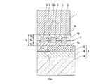
- FIG. 2 is an enlarged view of a portion A in FIG. 1, that is, a joint portion between the semiconductor chip 1 and the wiring member 7.
- the semiconductor chip 1 includes a semiconductor layer 1A such as SiC and an electrode layer (1B, 1C).
- the electrode layer (1B, 1C) has an electrode metal layer 1B such as Al or Al alloy, and an outer plated metal layer 1C such as silver (Ag) or gold (Au).
- the joint portion 2 includes a sintered metal layer 4a arranged on the outer plated metal layer 1C, a sintered metal layer 4b arranged on the sintered metal layer 4a and below the wiring member 7, and a sintered metal.
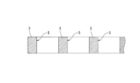
- a metal plate 3 arranged between the layer 4a and the sintered metal layer 4b and having a plurality of through holes 5 is provided.
- the portion filled with the sintered metal layer 4a is the first groove portion 15a
- the portion filled with the sintered metal layer 4b is the second groove portion 15b.
- a plurality of circular through holes 5 are arranged in a matrix on the metal plate 3 in a plan view.
- the through hole 5 has the same diameter on the upper and lower surfaces of the metal plate 3.
- the arrangement of the through holes 5 is not limited to the matrix shape, and may be a striped shape arrangement or a random arrangement.
- the shape of the through hole 5 is not limited to a circular shape, and may be an elliptical shape, a rectangular shape, a polygonal shape, or the like.
- the first sintered metal layer 4a has a plurality of regions having different tensile strengths.
- the second sintered metal layer 4b has a plurality of regions having different tensile strengths.
- the metal plate 3 (metal material) is arranged between a part of the first sintered metal layer 4a having a high tensile strength and a part of the second sintered metal layer 4b having a high tensile strength. ..
- the sintered metal layers (4a, 4b) are a first sintered metal layer 4a arranged on the first semiconductor chip 1 side of the metal material 3 and a second arranged on the first wiring member 7 side of the metal material 3.
- the metal material 3 is a first metal plate 3 having a sintered metal layer 4b and a plurality of first groove portions 15a on the lower surface and a plurality of second groove portions 15b on the upper surface, and the first groove portion 15a and the second groove portion 15a. There is a region of the flat surface portion 3e in which the groove portion 15b is not formed.
- FIG. 5 is an enlarged view of the C portion in FIG. 1, that is, the junction portion between the semiconductor chip 1 and the insulating circuit board 8.
- the semiconductor chip 1 includes a semiconductor layer 1A such as SiC and an electrode layer (1D, 1E).
- the electrode layer (1D, 1E) has an electrode metal layer 1D such as Al or Al alloy, and an outer plated metal layer 1E such as silver (Ag) or gold (Au).
- the joint portion 2a is a sintered metal layer 4c arranged under the outer plated metal layer 1E, and a sintered metal layer 4d arranged on the conductor layer 82a of the insulating circuit substrate 8 under the sintered metal layer 4c.
- the metal plate 3a has a plurality of circular through holes 5a arranged in a matrix in a plan view.
- the shape of the through hole 5a is not limited to a circular shape, and may be an elliptical shape, a rectangular shape, a polygonal shape, or the like.
- the arrangement of the through holes 5a is not limited to the matrix shape, and may be a staggered arrangement, a striped arrangement, or a random arrangement.
- Nanometer-sized Ag nanoparticles are used as the material for the sintered metal layers 4a, 4b, 4c, and 4d.
- the material of the sintered metal layers 4a, 4b, 4c, and 4d may be a composite containing a micrometer-sized Ag powder in Ag nanoparticles.
- a metal such as Ag or Au is desirable in consideration of bonding with the sintered metal layers 4a and 4b.
- the metal plate 3 may be a metal plate in which the surface of copper (Cu), Al, Al alloy or the like is Ag-plated or Au-plated. It is desirable to use sintered metal for the joints 6 and 9 shown in FIG. 1, but since it is separated from the semiconductor chip 1 which is the heat source, a normal solder or other joint member may be used.
- sintered metal has a tensile strength (hereinafter, also simply referred to as strength), for example, a yield stress represented by 0.2% proof stress (hereinafter, also simply referred to as yield stress) of 3. It can be doubled to four times higher. Further, the yield stress can be increased by about 5 times as compared with Al or Al alloy which is an electrode material of a semiconductor element.
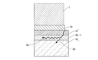
- the semiconductor chip 1 and the wiring member 7 such as a lead frame can be joined by a sintered metal layer 4z made of Ag nanoparticles.
- the entire wiring member 7 repeatedly undergoes thermal expansion and contraction in an energization cycle test, so that the sintered metal layer 4z, which is a bonded portion, is repeatedly strained. Since the sintered metal layer 4z as the joint portion has sufficient strength against the stress applied repeatedly, crack Ca easily extends to the electrode metal layer 1B made of low-strength Al or Al alloy. It is also conceivable that the generated crack Cb may extend to the semiconductor layer 1A of the semiconductor chip 1. As a result, the electrodes of the semiconductor chip 1 may deteriorate, resulting in an early failure.
- the strength of the sintered metal layers 4a and 4b is controlled by using the metal plate 3 having the through holes 5 between the sintered metal layers 4a and 4b.
- the relationship of the cross-sectional structure of the joint with respect to the pressurization of the sintered metal will be described with reference to FIGS. 7 to 12.
- Ag nanoparticles in which Ag nanoparticles are dispersed in a solvent are deposited on a flat base layer such as metal by a printing method. After deposition, it is dried to remove the solvent.
- the sintered metal layer made of Ag nanoparticles after solvent drying is about 1/2 the thickness of the accumulated Ag nanoparticles.
- the thickness of the sintered metal layer after solvent drying is defined as "supply thickness".
- a sheet-shaped or preform-shaped sintered metal layer made of Ag nanoparticles may be used. In this case, the solvent drying procedure can be omitted.
- the sintered metal layer thus formed is pressed with a press while being heated at a temperature in the range of 200 ° C. or higher and 300 ° C. or lower, for example, 250 ° C. to bond with the base layer.
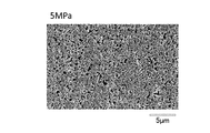
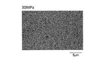
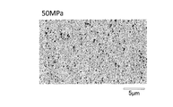
- the joint cross-sectional structure of each of the sintered metal layers laminated by changing the pressing force in the range of 0.25 MPa to 50 MPa was observed with a scanning electron microscope (SEM).
- SEM scanning electron microscope
- the thickness of the sintered metal layer after pressurization is defined as "laminated thickness”.
- FIGS. 7 to 12 show SEM images of the cross-sectional structure of each sintered metal layer laminated by changing the pressure in the range of 0.25 MPa to 50 MPa.
- the bright portion is the sintered metal layer and the dark portion is the void.
- the size of the voids is large and the sintering density of the sintered metal is low.
- the size of the voids decreases sharply as shown in FIGS. 9 and 10.
- the pressing force is increased from 30 MPa to 50 MPa, as shown in FIGS. 11 and 12
- the size of the voids becomes extremely small, and it can be seen that the sintered metal layer is densified.
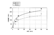
- 13 and 14 show the relationship between the tensile strength and the sintering density of the sintered metal layer pressurized by changing the pressure in the range of 0.25 MPa to 50 MPa.
- the yield stress and the maximum stress represented by 0.2% proof stress increase sharply from 0 to 10 MPa under pressure and gradually increase from 10 MPa to 50 MPa under pressure.
- the sintering density also increases sharply from 0 to 10 MPa, and gradually increases when the pressure ranges from 10 MPa to 50 MPa.
- the sintered powders of the sintered metal layer come close to each other to increase the sintering density, and the tensile strength of the sintered metal layer increases. It shows that it will increase.
- FIG. 15 shows the relationship between the sintering density of the sintered metal layer and the tensile strength.
- the yield stress of the sintered metal layer depends on the sintering density.
- the 100% of the amount of change in the laminated thickness in the thickness direction with respect to the supply thickness of the sintered metal layer is defined as "compression rate".
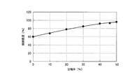
- compression rate the “compression rate” can be obtained from the amount of change in the sintering density.
- FIG. 16 shows the relationship between the compressibility and the sintering density. As shown in FIG.
- FIG. 17 shows the relationship between the compressibility and the tensile strength. As the compressibility of the sintered metal layer increases, the tensile strength increases. Further, considering that the compression of the sintered metal layer occurs substantially one-dimensionally in the pressurizing direction, the lamination thickness of the sintered metal layer can be obtained by using the compressibility or the sintering density.
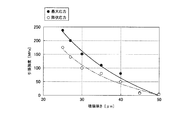
- FIG. 18 shows the relationship between the laminated thickness and the tensile strength. As shown in FIG. 18, the tensile strength decreases as the laminated thickness of the sintered metal layer increases.
- the strength corresponding to the yield stress of the sintered metal layer can be controlled by the pressure of pressurization by the press machine.
- the strength of the yield stress of the sintered metal layer can also be detected by the sintering density, compressibility, and stacking thickness of the sintered metal layer.
- the sintering densities of the sintered metal layers 4a and 4b are controlled so as to have the same or lower strength than the electrode metal layer 1B of the semiconductor chip 1, and the stress generated when the semiconductor device is energized is controlled. Disperse at the joint 2.
- the metal plate 3 having the through holes 5 is formed into the sintered metal layer 4a and the sintered metal layer. It is provided between 4b.
- FIG. 19 shows an Al alloy having a purity of 99.99% (4N) and an Al alloy containing 1.0% Si (Al-1.0% Si alloy) used for the electrode metal layer 1B, with a diameter of 6 mm.
- the result of the tensile strength test using the test piece with the reference point distance of 30 mm is shown.
- the yield stress is about 27 MPa for Al metal and about 35 MPa for Al-1.0% Si alloy. Therefore, in order to prevent the occurrence of cracks in the electrode metal layer 1B, the strength of the sintered metal layers 4a and 4b is controlled to a strength equal to or less than the tensile strength of Al or Al alloy, for example, in the range of 20 MPa to 40 MPa.
- the sintering density may be in the range of 72% or more and 78% or less.
- the compression ratio may be in the range of 10% or more and 20% or less.
- the thickness Tm of the metal plate 3 is less than 50% of the supply thickness or less than 63% of the laminated thickness.
- the thickness Tm of the metal plate 3 becomes 50% or more of the supply thickness, the compression ratio of each of the sintered metal layers 4a and 4b in the upper and lower regions of the metal plate 3 increases, so that the region of the through hole 5 is pressurized. There is a possibility of shortage. In that case, the contact area between the semiconductor chip 1 and the insulating circuit board 8 is reduced, the bonding strength is reduced, and the thermal resistance is increased.
- the conventional method for heating and pressurizing a sintered metal layer is used.
- the thickness Tm of the metal plate 3 is required to some extent.
- the strength of the sintered metal layers 4a and 4b in the region of the through hole 5 shown in FIG. 2 is controlled in the range of 20 MPa to 40 MPa, for example, about 35 MPa. To do. At this time, the sintering density is about 76% and the compression rate is about 18%. For example, assuming that the supply thickness of the sintered metal layers 4a and 4b in the region of the through hole 5 is about 100 ⁇ m, the laminated thickness Ts shown in FIG. 2 is about 82 ⁇ m, that is, the amount of deformation due to compression is about 18 ⁇ m.
- the sintering densities of the sintered metal layers 4a and 4b in the upper and lower regions of the metal plate 3 are larger than 76% and smaller than 90%.
- the supply thickness of the sintered metal layers 4a and 4b is preferably in the range of 50 ⁇ m or more and 1000 ⁇ m or less, and the laminated thickness is in the range of 41 ⁇ m or more and 820 ⁇ m or less.
- a metal plate 3 having a through hole 5 is provided between the sintered metal layer 4a and the sintered metal layer 4b to apply stress generated during energization. Disperse at the joint 2.
- the upper and lower regions of the metal plate 3 have higher strength of the sintered metal layers 4a and 4b than the regions of the through holes 5.
- the region of the through hole 5 having low strength of the sintered metal layers 4a and 4b is localized surrounded by the upper and lower regions of the metal plate 3 having high strength.
- the thickness Tb of the sintered metal layer 4b between the metal plate 3 and the wiring member 7 is thicker than the thickness Ta of the sintered metal layer 4a between the metal plate 3 and the semiconductor chip 1. desirable.
- the strength of the sintered metal layer 4b becomes smaller than that of the sintered metal layer 4a, and cracks occur in the sintered metal layer 4b on the wiring member 7 side of the metal plate 3 to form a semiconductor. It is possible to prevent the chip 1 from extending to the side.
- the occupied area of the opening of the through hole 5 is 25% or more and 75% or less with respect to the total area including the surface of the metal plate 3 and the opening of the through hole 5.
- the occupied area of the through hole 5 is less than 25%, the ratio of the high-strength portion in the sintered metal layers 4a and 4b increases, and the possibility that cracks occur in the electrode metal layers 1B and 1D increases.
- the occupied area exceeds 75%, the ratio of low-strength portions in the sintered metal layers 4a and 4b increases, and the possibility of cracks occurring in the sintered metal layers 4a and 4b increases.
- the strength of the sintered metal layer 4b on the wiring member 7 side smaller than that on the sintered metal layer 4a on the semiconductor chip 1 side, as shown in FIG. 20, occupy the opening of the through hole 5b of the metal plate 3b.
- the area may be adjusted.
- the opening size w1 of the first groove portion 55a on the semiconductor chip side is smaller than the opening size w2 of the second groove portion 55b on the wiring member 7 side. Therefore, the strength of the sintered metal layer 4b on the wiring member 7 side can be made smaller than that on the sintered metal layer 4a on the semiconductor chip 1 side.
- a metal plate 3c having a through hole 5c having an inclined side wall in which the opening size w2 on the wiring member 7 side is smaller than the opening size w1 on the semiconductor chip 1 side may be used.
- the strength of the sintered metal layers 4c and 4d in the region of the through hole 5a shown in FIG. 5 is in the range of 20 MPa or more and 40 MPa or less, for example, 35 MPa. Control to degree.
- the laminated thickness Ts shown in FIG. 5 is about 82 ⁇ m, that is, the amount of deformation due to compression is about 9 ⁇ m.
- the sintering density is about 76% and the compression rate is about 18%.
- the thickness Tm of the metal plate 3a is preferably less than 50% of the supply thickness.
- the firing between the metal plate 3a and the wiring layer 82a of the insulating circuit substrate 8 is compared with the thickness Tc of the sintered metal layer 4c between the metal plate 3a and the semiconductor chip 1. It is desirable that the thickness Td of the metal forming layer 4d is thin. By making the sintered metal layer 4d thinner, the strength of the sintered metal layer 4d becomes smaller than that of the sintered metal layer 4c, and cracks occur in the sintered metal layer 4d on the wiring layer 82a side of the metal plate 3a to form a semiconductor. It is possible to prevent the chip 1 from extending to the side.
- an insulating circuit with the semiconductor chip 1 side as shown in FIGS. 20 and 21 in order to make the strength of the sintered metal layer 4d on the insulating circuit board 8 side smaller than that on the sintered metal layer 4c on the semiconductor chip 1 side, an insulating circuit with the semiconductor chip 1 side as shown in FIGS. 20 and 21.
- a metal plate having a different opening size from that of the substrate 8 side may be used.
- a method of manufacturing the semiconductor device according to the first embodiment will be described with reference to FIGS. 1 and 2.
- a sintered metal paste in which Ag nanoparticles are dispersed in a solvent is applied to the upper surface of the electrode layers (1B, 1C) of the semiconductor chip 1 bonded to the wiring layer 82a of the insulating circuit board 8 by a printing method or a dispensing method. Apply by etc.
- the applied sintered metal paste is dried in a temperature range of 100 ° C. or higher and 150 ° C. or lower so that sintering of the sintered metal does not occur to remove the solvent, and the sintered metal layer 4a is laminated.
- a metal plate 3 having a plurality of through holes 5 is arranged on the sintered metal layer 4a.
- a sintered metal paste in which Ag nanoparticles are dispersed in a solvent is applied onto the metal plate 3 by a printing method, a dispensing method, or the like.
- the applied sintered metal paste is dried in a temperature range of 100 ° C. or higher and 150 ° C. or lower to remove the solvent, and the sintered metal layer 4b is laminated.
- the joint portion 2 having the sintered metal layer 4a, the metal plate 3, and the sintered metal layer 4b is formed on the upper surface of the semiconductor chip 1.
- the sintered metal layers 4a and 4b are physically connected to each other in the through hole 5.
- a wiring member 7 such as a lead frame is arranged on the joint portion 2, and the sintered metal layers 4a and 4b are placed on the wiring member 7 from above the wiring member 7 by a pressure forming apparatus such as a press machine in a range of 200 ° C. or higher and 300 ° C. or lower. For example, pressurize while heating at 250 ° C. Pressurization is performed at a pressure in which the compressibility of the sintered metal layers 4a and 4b is in the range of 10% or more and 20% or less in the region of the through hole 5. By pressurization, the semiconductor chip 1 and the sintered metal layer 4a, and the sintered metal layer 4b and the wiring member 7 are joined.
- the sintered metal layers 4a and 4b are metallurgically connected, and the sintering density of the sintered metal layers 4a and 4b is in the range of 72% or more and 78% or less.
- the sintering densities of the sintered metal layers 4a and 4b are higher than those in the sintered metal layers 4a and 4b in the region of the through hole 5. In this way, a semiconductor device in which the semiconductor chip 1 is bonded to the insulating circuit board 8 and the wiring member 7 by the sintered metal layers 4a and 4b is manufactured.
- the sintered metal paste is used for laminating the sintered metal layers 4a and 4b, but a sintered metal layer made of sheet-shaped or preform-shaped Ag nanoparticles may be used. Further, as the joint portion 2, a multilayer plate (clad material) in which a sintered metal layer is previously arranged on the front and back surfaces of a metal plate having through holes may be used.
- the difference in thickness may be adjusted by a cushioning member such as heat-resistant rubber arranged between the press mold of the pressure forming apparatus and the semiconductor apparatus.
- a cushioning member such as heat-resistant rubber arranged between the press mold of the pressure forming apparatus and the semiconductor apparatus.
- a cushioning member such as heat-resistant rubber arranged between the press mold of the pressure forming apparatus and the semiconductor apparatus.
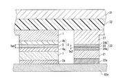
- a semiconductor chip (first semiconductor chip) 1 such as an IGBT or MOSFET and a semiconductor chip (second semiconductor chip) 21 such as FWD or SBD are used.
- the semiconductor chip 1 is bonded to the wiring layer 82a via the bonding portion 2a.
- One end of the wiring member 7 is joined to the semiconductor chip 1 via the joint portion 2.
- the other end of the wiring member 7 is joined to the wiring layer 82b via the joint portion 6.
- the semiconductor chip 21 is bonded to the wiring layer 82a via the bonding portion 22a.
- One end of the wiring member 27 is joined to the semiconductor chip 21 via the joining portion 22.
- the other end of the wiring member 27 is joined to the wiring layer 82c via the joint portion 26.
- the joint portions 22 and 22a have a structure in which a metal plate having through holes is sandwiched between sintered metal layers, similarly to the joint portions 2 and 2a shown in FIGS. 2 and 5.
- the portion of the semiconductor chip 21 in contact with the wiring member 27 is larger than the portion of the semiconductor chip 1 in contact with the wiring member 7. make it thin. In this way, it is possible to collectively join with the press mold 31 of the pressure forming apparatus via the buffer member 32.
- the joint portion 2 includes a sintered metal layer 4a, a sintered metal layer 4b, and a metal plate 3.
- the metal plate 3 is arranged between the sintered metal layer 4a and the sintered metal layer 4b, and has through holes (not shown).
- the joint portion 22 includes a sintered metal layer 24a, a sintered metal layer 24b, and a metal plate 23.
- the metal plate 23 is arranged between the sintered metal layer 24a and the sintered metal layer 24b, and has a through hole (not shown).
- the thickness Tm2 of the metal plate 23 is made thinner than the thickness Tm1 of the metal plate 3, so that the upper surfaces of the wiring member 7 of the semiconductor chip 1 and the wiring member 27 of the semiconductor chip 21 are at the same level.
- the cushioning member 32 arranged on the pressure surface of the press mold 31 can be in contact with the wiring members 7 and 27 on a flat surface, and can be joined together.
- the level of the upper surfaces of the wiring members 7 and 27 may be adjusted by the thickness of the metal plate used for each of the joint portion 2a of the semiconductor chip 1 and the joint portion 22a of the semiconductor chip 21.
- the level of the upper surface of the wiring members 7 and 27 may be adjusted by the sum of the thicknesses of the metal plates of the joints 2 and 2a and the sum of the thicknesses of the metal plates of the joints 22 and 22a.
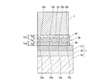
- the semiconductor device according to the second embodiment joins the semiconductor chip 1, the semiconductor chip 1 and the insulating circuit board 8 as shown in FIG. 24.
- a joint portion 2c and a joint portion 2b for joining the semiconductor chip 1 and the wiring member 7 are provided.
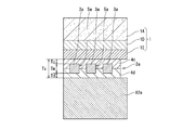
- the joint portion 2b is arranged between the electrode layer (1B, 1C) and the wiring member 7.
- the joint portion 2b is arranged between the sintered metal layer 4e arranged on the outer plated metal layer 1C, the sintered metal layer 4f arranged under the wiring member 7, and the sintered metal layers 4e and 4f.
- a metal plate 3d is provided.
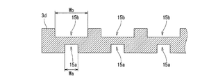
- the metal plate 3d has a plurality of first groove portions 15a and a plurality of second groove portions 15b independently on the lower surface and the upper surface, respectively.
- the plurality of first groove portions 15a are provided on the side of the metal plate 3d facing the semiconductor chip 1.
- the plurality of second groove portions 15b are provided on the side of the metal plate 3d facing the wiring member 7.
- the second embodiment is different from the first embodiment in that it has a metal plate 3d having a plurality of first groove portions 15a and a plurality of second groove portions 15b independently on the lower surface and the upper surface. Since the other configurations are the same as those in the first embodiment, duplicate descriptions will be omitted.
- a plurality of circular first groove portions 15a are arranged on the lower surface and a plurality of circular second groove portions 15b are arranged on the upper surface in a matrix in a plan view.
- the shapes of the first and second groove portions 15a and 15b are not limited to a circular shape, and may be an elliptical shape, a rectangular shape, a polygonal shape, or the like. Further, the arrangement of the first and second groove portions 15a and 15b is not limited to the matrix shape, and may be a striped shape arrangement or a random arrangement.
- the plurality of first groove portions 15a are provided on the side of the metal plate 3d facing the semiconductor chip 1 and have a depth Da.
- the plurality of second groove portions 15b are provided on the side of the metal plate 3d facing the wiring member 7, and have a depth Db.
- the depth Da and the depth Db may be the same or different.
- a metal such as Ag or Au is desirable in consideration of bonding with the sintered metal layers 4a and 4b containing Ag particles, Ag powder and the like.
- the metal plate 3d may be a metal plate in which the surface of Cu, Al, Al alloy or the like is Ag-plated or Au-plated.
- the strength of the sintered metal layers 4e and 4f is controlled by using the metal plates 3d having the first and second groove portions 15a and 15b between the sintered metal layers 4e and 4f. To do.
- the sintering densities of the sintered metal layers 4e and 4f are controlled so that the strength is equal to or less than that of the electrode metal layer 1B of the semiconductor chip 1, and the stress generated when the semiconductor device is energized is dispersed at the joint portion 2b. ..
- the yield stress is about 27 MPa for Al metal and about 35 MPa for Al-1.0% Si alloy. Therefore, the strength of the sintered metal layers 4e and 4f is controlled in the range of 20 MPa or more and 40 MPa or less.
- the sintering density may be in the range of 72% or more and 78% or less.
- the compression ratio may be in the range of 10% or more and 20% or less.
- the thickness Tm of the metal plate 3d is less than 50% of the supply thickness.
- the compression ratios of the sintered metal layers 4e and 4f in the region above the metal plate 3d increase, so that the first and second groove portions 15a, There is a possibility that the pressurization of each region of 15b will be insufficient. In that case, the contact area between the semiconductor chip 1 and the insulating circuit board 8 is reduced, the bonding strength is reduced, and the thermal resistance is increased.
- the conventional method for heating and pressurizing a sintered metal layer is used.
- the sintering density can be controlled because the pressurization may be excessive or insufficient depending on the position. It disappears. Therefore, the thickness Tm of the metal plate 3d is required to some extent. Further, the depths Da and Db of the first and second groove portions 15a and 15b are preferably larger than 0 and smaller than the thickness Tm of the metal plate 3d.
- the strength of the sintered metal layers 4e and 4f in the regions of the first and second groove portions 15a and 15b shown in FIG. 25 is 20 MPa or more and 40 MPa or less.
- the range is controlled to, for example, about 35 MPa.
- the sintering density is about 76% and the compression rate is about 18%.
- the laminated thickness Tsa of the sintered metal layer 4e and the laminated thickness Tsb of the sintered metal layer 4e shown in FIG. 25 are each about 82 ⁇ m.
- the amount of deformation due to compression is about 18 ⁇ m.
- the depths Da and Db of the first and second groove portions 15a and 15b are larger than 0 and smaller than the thickness Tm of the metal plate 3d, the sintered metal layer 4a in the region above the metal plate 3d, The sintering density of 4b is greater than 76% and less than 90%.
- a metal plate 3d having the first and second groove portions 15a and 15b is provided between the sintered metal layer 4e and the sintered metal layer 4f.
- the stress generated during energization is dispersed at the joint portion 2b.
- the regions on the metal plate 3d have higher strength of the sintered metal layers 4e and 4f than the regions on the first and second groove portions 15a and 15b.
- the regions of the sintered metal layers 4e and 4f on the first and second groove portions 15a and 15b having low strength are localized surrounded by the regions having high strength. Therefore, even if cracks occur in the regions of the sintered metal layers 4e and 4f on the first and second groove portions 15a and 15b, they can be prevented from extending to the entire sintered metal layers 4e and 4f.
- the depth Db of the second groove portion 15b of the metal plate 3d is deeper than the depth Da of the first groove portion 15a of the metal plate 3d.
- the strength of the sintered metal layer 4f becomes smaller than that of the sintered metal layer 4e, and cracks are generated in the sintered metal layer 4f on the wiring member 7 side of the metal plate 3d to generate a semiconductor chip. It is possible to prevent the extension to one side. As a result, deterioration of the semiconductor chip 1 can be prevented, and the reliability of the semiconductor device can be improved.
- the occupied areas of the first groove portion 15a and the second groove portion 15b are equal to the total area of the metal plate 3d including the surface of the metal plate 3d and the opening of the first groove portion 15a or the opening of the second groove portion 15b.
- the thickness Tb of the sintered metal layer 4f between the metal plate 3d and the wiring member 7 is thicker than the thickness Ta of the sintered metal layer 4e between the metal plate 3d and the semiconductor chip 1. desirable.
- the strength of the sintered metal layer 4f becomes smaller than that of the sintered metal layer 4e, and cracks occur in the sintered metal layer 4f on the wiring member 7 side of the metal plate 3d to form a semiconductor. It is possible to prevent the chip 1 from extending to the side.
- the first and second groove portions 15a of the metal plate 3d may be adjusted.
- the opening size Wa of the first groove portion 15a on the semiconductor chip side is smaller than the opening size Wb of the second groove portion 15b on the wiring member 7 side. Therefore, the strength of the sintered metal layer 4f on the wiring member 7 side can be made smaller than that on the sintered metal layer 4e on the semiconductor chip 1 side.
- the joining portion 2c fires a metal plate having the first and second groove portions 15a and 15b shown in FIG. It has a structure that is placed between the metal layers.
- the strength of the sintered metal layer in the regions of the first and second groove portions 15a and 15b is controlled in the range of 20 MPa or more and 40 MPa or less, for example, about 35 MPa.
- the supply thickness of the sintered metal layer is about 100 ⁇ m
- the laminated thicknesses Tsa and Tsb shown in FIG. 25 are each about 82 ⁇ m, that is, the amount of deformation due to compression is about 18 ⁇ m.
- the sintering density is about 76% and the compression rate is about 18%.
- the thickness Tm of the metal plate is preferably less than 50% of the supply thickness.
- the thickness of the sintered metal layer between the metal plate of the joint portion 2c and the semiconductor chip 1 shown in FIG. 24 is compared with the thickness of the sintered metal between the metal plate and the wiring layer 82a of the insulating circuit board 8. It is desirable that the layer thickness is thin.
- the strength of the sintered metal layer on the insulating circuit board 8 side becomes smaller than that on the semiconductor chip 1 side, and cracks are generated in the wiring of the joint portion 2c. It is possible to prevent the sintered metal layer on the layer 82a side from being generated and extending to the semiconductor chip 1 side.
- the metal plate 3, 3d may be any one of metal particles, metal fibers, and metal nets.
Landscapes
- Die Bonding (AREA)
- Engineering & Computer Science (AREA)
- Cooling Or The Like Of Semiconductors Or Solid State Devices (AREA)
- Chemical & Material Sciences (AREA)
- Ceramic Engineering (AREA)
- Manufacturing & Machinery (AREA)
Abstract
Description
本発明の半導体装置は、表面に金属層を有する第1半導体チップと、金属層に対向して配置された第1配線部材と、金属層と第1配線部材との間に配置され、引張強度が高い複数の領域および引張強度が低い複数の領域を備えた焼結金属層と、焼結金属層の内部に配置された金属材料と、を備え、焼結金属層の一部の引張強度の低い領域の引張強度は、第1半導体チップの金属層の引張強度より低い。本発明の第1実施形態に係る半導体装置は、図1に示すように、半導体チップ(第1半導体チップ)1、接合部2,2a、絶縁回路基板8、及び配線部材7を備える。絶縁回路基板8は、絶縁板81、絶縁板81の上面にパターニングされた導体層(配線層)82a、82b、及び絶縁板81の下面に設けられた導体層(放熱層)83を有する。半導体チップ1の上面は、接合部2を介して配線部材7の一端に電気的に接続される。半導体チップ1の下面は、接合部2aを介して絶縁回路基板8の導体層82aに電気的に接続される。配線部材7の他端が、接合部6を介して絶縁回路基板8の導体層82bに電気的に接続される。絶縁回路基板8の導体層83は、接合部9を介して放熱ベース10に接続される。
第1焼結金属層4aは、引張強度の異なる複数の領域を有する。第2焼結金属層4bは、引張強度の異なる複数の領域を有する。金属板3(金属材料)は、第1焼結金属層4aの一部の引張強度が高い領域と第2焼結金属層4bの一部の引張強度が高い領域との間に配置されている。
焼結金属層(4a,4b)は、金属材料3の第1半導体チップ1側に配置された第1焼結金属層4aと、金属材料3の第1配線部材7側に配置された第2焼結金属層4bとを有し、金属材料3は、下面に複数の第1溝部15a、上面に複数の第2溝部15bを有する第1金属板3であって、第1溝部15aおよび第2溝部15bが形成されていない平面部3eの領域がある。
第2実施形態に係る半導体装置は、図24に示すように、第1実施形態に係る半導体装置は、図24に示すように、半導体チップ1、半導体チップ1と絶縁回路基板8とを接合する接合部2c、及び半導体チップ1と配線部材7とを接合する接合部2bを備える。図24中のD部分の拡大図である図25に示すように、接合部2bは、電極層(1B,1C)と配線部材7との間に配置される。接合部2bは、外側めっき金属層1Cの上に配置された焼結金属層4e、配線部材7の下に配置された焼結金属層4f、及び焼結金属層4e、4fの間に配置された金属板3dを備える。金属板3dは、複数の第1溝部15a及び複数の第2溝部15bを、下面及び上面にそれぞれ独立して有する。複数の第1溝部15aは、金属板3dの半導体チップ1に面する側に設けられる。複数の第2溝部15bは、金属板3dの配線部材7に面する側に設けられる。第2実施形態は、複数の第1溝部15a及び複数の第2溝部15bを、下面及び上面にそれぞれ独立して有する金属板3dを有する点が第1実施形態と異なる。他の構成は第1実施形態と同様であるので重複する記載は省略する。
本発明は上記の開示した実施形態によって説明したが、この開示の一部をなす論述及び図面は、本発明を限定するものであると理解すべきではない。本発明の明細書や図面の開示から当業者には様々な代替実施形態、実施例及び運用技術が明らかになると考えられるべきである。又、上記の実施形態及び各変形例において説明される各構成を任意に応用した構成等、本発明はここでは記載していない様々な実施形態等を含むことは勿論である。したがって、本発明の技術的範囲は上記の例示的説明から妥当な、特許請求の範囲に係る発明特定事項によってのみ定められるものである。
1A…半導体層
1B,1D…電極金属層
1C,1E…外側めっき金属層
2,2a,2b,2c,6,9,22,22a,26…接合部
3,3a,3b,3c,3d,23…金属板
3e…平面部
4a,4b,4c,4d,4e,4f,24a,24b…焼結金属層
5,5a,5b,5c…貫通孔
7,27…配線部材
8…絶縁回路基板10…放熱ベース
15a,55a…第1溝部
15b,55b…第2溝部
31…プレス型
32…緩衝部材
81…絶縁板
82a,82b,82c…導体層(配線層)
83…導体層(放熱層)
Claims (19)
- 表面に金属層を有する第1半導体チップと、
前記金属層に対向して配置された第1配線部材と、
前記金属層と前記第1配線部材との間に配置され、引張強度が高い複数の領域および引張強度が低い複数の領域を備えた焼結金属層と、
前記焼結金属層の内部に配置された金属材料と、
を備え、
前記焼結金属層の一部の引張強度の低い領域の引張強度は、前記第1半導体チップの前記金属層の引張強度より低いことを特徴とする半導体装置。 - 前記焼結金属層は、前記金属材料の前記第1半導体チップ側に配置された第1焼結金属層と、前記金属材料の前記第1配線部材側に配置された第2焼結金属層とを有し、
前記金属材料は、下面に複数の第1溝部、上面に複数の第2溝部を有する第1金属板であって、前記第1溝部および前記第2溝部が形成されていない平面部の領域があることを特徴とする請求項1に記載の半導体装置。 - 前記複数の第1溝部及び前記複数の第2溝部は、それぞれ互いに接続した複数の貫通孔をなすことを特徴とする請求項2に記載の半導体装置。
- 前記複数の第1溝部及び第2溝部のそれぞれの領域における前記第1焼結金属層及び第2焼結金属層の焼結密度は、72%以上、78%以下の範囲であることを特徴とする請求項2又は3に記載の半導体装置。
- 前記第1焼結金属層の焼結密度は、前記複数の第1溝部の領域に比べて前記第1金属板の前記下面の領域の方が高く、
前記第2焼結金属層の焼結密度は、前記複数の第2溝部の領域に比べて前記第1金属板の前記上面の領域の方が高いことを特徴とする請求項2~4のいずれか1項に記載の半導体装置。 - 前記複数の第1溝部の領域の前記第1焼結金属層の焼結密度は、前記複数の第2溝部の領域の前記第2焼結金属層の焼結密度に比べて高いことを特徴とする請求項2~5のいずれか1項に記載の半導体装置。
- 平面パターンにおいて、前記複数の第1溝部及び前記第2溝部のそれぞれの占有面積が前記第1金属板の表面積に対して25%以上75%以下であることを特徴とする請求項2~6のいずれか1項に記載の半導体装置。
- 平面パターンにおいて、前記複数の第1溝部の占有面積が前記複数の第2溝部の占有面積に比べて小さいことを特徴とする請求項2~7のいずれか1項に記載の半導体装置。
- 前記第1金属板の厚さが、前記第1半導体チップの表面から前記第1溝部の底部までの前記第1焼結金属層の厚さの0%より大きく63%以下の範囲であることを特徴とする請求項2~8のいずれか1項に記載の半導体装置。
- 前記第1半導体チップの上面から前記第1溝部の底部までの前記第1焼結金属層の厚さが、前記第1配線部材の下面から前記第2溝部の底部までの前記第2焼結金属層の厚さに比べて薄いことを特徴とする請求項2~9のいずれか1項に記載の半導体装置。
- 第2半導体チップと、
前記第2半導体チップの上方に配置され、下面に複数の第3溝部、上面に複数の第4溝部を有する第2金属板と、
前記第2金属板の上方に配置された第2配線部材と、
前記複数の第3溝部を埋めるように前記第2半導体チップと前記第2金属板との間に配置された第3焼結金属層と、
前記複数の第4溝部を埋めるように前記第2金属板と前記第2配線部材との間に配置された第4焼結金属層と
を更に備え、
前記第1配線部材及び前記第2配線部材の上面の高さのレベルが同一であることを特徴とする請求項1~10のいずれか1項に記載の半導体装置。 - 前記第1金属板及び前記第2金属板の厚さが異なることを特徴とする請求項11に記載の半導体装置。
- 前記第1半導体チップの下方に配置され、上面に複数の第5溝部、下面に複数の第6溝部を有する第3金属板と、
前記第3金属板の下方に配置され、上面に配線層を有する絶縁回路基板と、
前記複数の第5溝部を埋めるように前記第1半導体チップと前記第3金属板との間に配置された第5焼結金属層と、
前記複数の第6溝部を埋めるように前記第3金属板と前記配線層との間に配置された第6焼結金属層と
を更に備えることを特徴とする請求項1~12のいずれか1項に記載の半導体装置。 - 前記金属材料が、金属粒子、金属繊維または金属ネットのいずれか1種類であることを特徴とする請求項1~13のいずれか1項に記載の半導体装置。
- 絶縁回路基板の上面に配置された配線層の上に第1半導体チップを接合するステップと、
前記第1半導体チップの上面に焼結金属ペーストを塗布して乾燥させ、第1焼結金属層を積層するステップと、
下面に複数の第1溝部、上面に複数の第2溝部を有する第1金属板を、前記第1焼結金属層の上に前記第1金属板の前記下面が接するように配置するステップと、
前記第1金属板の前記上面に焼結金属ペーストを塗布して乾燥させ、第2焼結金属層を積層するステップと、
前記第2焼結金属層の上に第1配線部材を配置するステップと、
前記第1焼結金属層及び第2焼結金属層を加熱しながら加圧して、前記第1焼結金属層を前記複数の第1溝部に充填するように前記第1金属板の前記下面と前記第1半導体チップとの間で接合させ、且つ、前記第2焼結金属層を前記複数の第2溝部に充填するように前記第1金属板の前記上面と前記第1配線部材との間で接合させるステップと
を備えることを特徴とする半導体装置の製造方法。 - 前記複数の第1溝部及び前記複数の第2溝部は、それぞれ互いに接続した複数の貫通孔をなすことを特徴とする請求項15に記載の半導体装置の製造方法。
- 前記第1焼結金属層及び第2焼結金属層の前記加圧は、前記焼結金属ペーストを乾燥させた後の前記第1焼結金属層及び第2焼結金属層の供給厚さに対して10%以上、20%以下の範囲の圧縮率で実施されることを特徴とする請求項15又は16に記載の半導体装置の製造方法。
- 前記絶縁回路基板の上に接合された第2半導体チップの上面に第3焼結金属層を形成するステップと、
下面に複数の第3溝部、上面に複数の第4溝部を有する第2金属板を、前記第3焼結金属層の上に前記第2金属板の前記下面が接するように配置するステップと、
前記第2金属板の前記上面に第4焼結金属層を形成するステップと、
前記第4焼結金属層の上に第2配線部材を配置するステップと、
前記第3焼結金属層及び第4焼結金属層を加熱しながら加圧して、前記第3焼結金属層を前記複数の第3溝部に充填するように前記第2金属板の前記下面と前記第2半導体チップとの間で接合させ、且つ、前記第4焼結金属層を前記複数の第4溝部に充填するように前記第2金属板の前記上面と前記第2配線部材との間で接合させるステップと
を備え、
前記第3焼結金属層及び第4焼結金属層の前記加圧は、前記第1焼結金属層及び第2焼結金属層の前記加圧と同時に実施されることを特徴とする請求項15~17のいずれか1項に記載の半導体装置の製造方法。 - 前記第1金属板及び前記第2金属板の厚さが異なり、且つ、前記第1配線部材及び前記第2配線部材の上面の高さのレベルが同一であることを特徴とする請求項18に記載の半導体装置の製造方法。
Priority Applications (3)
| Application Number | Priority Date | Filing Date | Title |
|---|---|---|---|
| JP2021527615A JP7238985B2 (ja) | 2019-06-20 | 2020-06-08 | 半導体装置及び半導体装置の製造方法 |
| CN202080006652.XA CN113169083B (zh) | 2019-06-20 | 2020-06-08 | 半导体装置以及半导体装置的制造方法 |
| US17/331,013 US12021043B2 (en) | 2019-06-20 | 2021-05-26 | Semiconductor device and method for manufacturing semiconductor device |
Applications Claiming Priority (2)
| Application Number | Priority Date | Filing Date | Title |
|---|---|---|---|
| JP2019114534 | 2019-06-20 | ||
| JP2019-114534 | 2019-06-20 |
Related Child Applications (1)
| Application Number | Title | Priority Date | Filing Date |
|---|---|---|---|
| US17/331,013 Continuation US12021043B2 (en) | 2019-06-20 | 2021-05-26 | Semiconductor device and method for manufacturing semiconductor device |
Publications (1)
| Publication Number | Publication Date |
|---|---|
| WO2020255773A1 true WO2020255773A1 (ja) | 2020-12-24 |
Family
ID=74037295
Family Applications (1)
| Application Number | Title | Priority Date | Filing Date |
|---|---|---|---|
| PCT/JP2020/022499 Ceased WO2020255773A1 (ja) | 2019-06-20 | 2020-06-08 | 半導体装置及び半導体装置の製造方法 |
Country Status (4)
| Country | Link |
|---|---|
| US (1) | US12021043B2 (ja) |
| JP (1) | JP7238985B2 (ja) |
| CN (1) | CN113169083B (ja) |
| WO (1) | WO2020255773A1 (ja) |
Cited By (1)
| Publication number | Priority date | Publication date | Assignee | Title |
|---|---|---|---|---|
| WO2022249805A1 (ja) * | 2021-05-27 | 2022-12-01 | 株式会社デンソー | 半導体装置 |
Families Citing this family (5)
| Publication number | Priority date | Publication date | Assignee | Title |
|---|---|---|---|---|
| JP7239051B2 (ja) * | 2020-03-04 | 2023-03-14 | 株式会社デンソー | 半導体装置およびその製造方法 |
| KR102916276B1 (ko) * | 2020-09-02 | 2026-01-22 | 에스케이하이닉스 주식회사 | 3차원 구조의 반도체 장치 |
| CN115312505A (zh) * | 2022-07-19 | 2022-11-08 | 湖南国芯半导体科技有限公司 | 一种功率器件的无引线封装结构及封装方法 |
| JP7748924B2 (ja) * | 2022-09-14 | 2025-10-03 | 株式会社東芝 | 半導体装置 |
| JP2024130953A (ja) * | 2023-03-15 | 2024-09-30 | 株式会社東芝 | 半導体装置およびその製造方法 |
Citations (11)
| Publication number | Priority date | Publication date | Assignee | Title |
|---|---|---|---|---|
| DE10349477A1 (de) * | 2003-10-21 | 2005-02-24 | Infineon Technologies Ag | Halbleiterbauteile mit einem Gehäuse und mit einem Halbleiterchip, sowie Verfahren zur Herstellung desselben |
| JP2006202586A (ja) * | 2005-01-20 | 2006-08-03 | Nissan Motor Co Ltd | 接合方法及び接合構造 |
| JP2006269682A (ja) * | 2005-03-23 | 2006-10-05 | Fuji Electric Holdings Co Ltd | 半導体装置およびその製造方法 |
| JP2011192695A (ja) * | 2010-03-12 | 2011-09-29 | Mitsubishi Electric Corp | 半導体装置 |
| JP2011238779A (ja) * | 2010-05-11 | 2011-11-24 | Mitsubishi Electric Corp | 導電性接合構造体、これを用いた半導体装置および半導体装置の製造方法 |
| JP2015216160A (ja) * | 2014-05-08 | 2015-12-03 | 三菱電機株式会社 | 電力用半導体装置および電力用半導体装置の製造方法 |
| WO2017002793A1 (ja) * | 2015-07-01 | 2017-01-05 | 三菱電機株式会社 | 半導体装置および半導体装置の製造方法 |
| JP2018026417A (ja) * | 2016-08-09 | 2018-02-15 | 三菱電機株式会社 | 電力用半導体装置 |
| DE102017206925A1 (de) * | 2017-04-25 | 2018-10-25 | Siemens Aktiengesellschaft | Verfahren zum Erzeugen einer Diffusionslötverbindung |
| EP3416186A1 (en) * | 2017-06-14 | 2018-12-19 | Infineon Technologies AG | Semiconductor substrate arrangement with a connection layer with regions of different porosity and method for producing the same |
| JP2019212759A (ja) * | 2018-06-05 | 2019-12-12 | 新光電気工業株式会社 | 半導体装置及び半導体装置の製造方法 |
Family Cites Families (10)
| Publication number | Priority date | Publication date | Assignee | Title |
|---|---|---|---|---|
| JP5240021B2 (ja) | 2009-04-03 | 2013-07-17 | 日産自動車株式会社 | 半導体装置及びその製造方法 |
| JP2010251457A (ja) | 2009-04-14 | 2010-11-04 | Nissan Motor Co Ltd | 半導体装置及びその製造方法 |
| JP2012138470A (ja) | 2010-12-27 | 2012-07-19 | Mitsubishi Electric Corp | 半導体素子、半導体装置および半導体装置の製造方法 |
| US8987879B2 (en) | 2011-07-06 | 2015-03-24 | Infineon Technologies Ag | Semiconductor device including a contact clip having protrusions and manufacturing thereof |
| JP5880300B2 (ja) | 2012-06-14 | 2016-03-08 | 日立化成株式会社 | 接着剤組成物及びそれを用いた半導体装置 |
| US10410945B2 (en) * | 2015-03-23 | 2019-09-10 | Hitachi, Ltd. | Semiconductor device |
| WO2016157866A1 (ja) | 2015-03-30 | 2016-10-06 | 日本ケミコン株式会社 | コンデンサおよびその製造方法 |
| US9620466B1 (en) | 2015-11-30 | 2017-04-11 | Infineon Technologies Ag | Method of manufacturing an electronic device having a contact pad with partially sealed pores |
| JP6643975B2 (ja) | 2016-12-28 | 2020-02-12 | 三菱電機株式会社 | 半導体装置の製造方法 |
| JP2018195724A (ja) * | 2017-05-18 | 2018-12-06 | 三菱電機株式会社 | パワーモジュールおよびその製造方法ならびに電力変換装置 |
-
2020
- 2020-06-08 WO PCT/JP2020/022499 patent/WO2020255773A1/ja not_active Ceased
- 2020-06-08 CN CN202080006652.XA patent/CN113169083B/zh active Active
- 2020-06-08 JP JP2021527615A patent/JP7238985B2/ja active Active
-
2021
- 2021-05-26 US US17/331,013 patent/US12021043B2/en active Active
Patent Citations (11)
| Publication number | Priority date | Publication date | Assignee | Title |
|---|---|---|---|---|
| DE10349477A1 (de) * | 2003-10-21 | 2005-02-24 | Infineon Technologies Ag | Halbleiterbauteile mit einem Gehäuse und mit einem Halbleiterchip, sowie Verfahren zur Herstellung desselben |
| JP2006202586A (ja) * | 2005-01-20 | 2006-08-03 | Nissan Motor Co Ltd | 接合方法及び接合構造 |
| JP2006269682A (ja) * | 2005-03-23 | 2006-10-05 | Fuji Electric Holdings Co Ltd | 半導体装置およびその製造方法 |
| JP2011192695A (ja) * | 2010-03-12 | 2011-09-29 | Mitsubishi Electric Corp | 半導体装置 |
| JP2011238779A (ja) * | 2010-05-11 | 2011-11-24 | Mitsubishi Electric Corp | 導電性接合構造体、これを用いた半導体装置および半導体装置の製造方法 |
| JP2015216160A (ja) * | 2014-05-08 | 2015-12-03 | 三菱電機株式会社 | 電力用半導体装置および電力用半導体装置の製造方法 |
| WO2017002793A1 (ja) * | 2015-07-01 | 2017-01-05 | 三菱電機株式会社 | 半導体装置および半導体装置の製造方法 |
| JP2018026417A (ja) * | 2016-08-09 | 2018-02-15 | 三菱電機株式会社 | 電力用半導体装置 |
| DE102017206925A1 (de) * | 2017-04-25 | 2018-10-25 | Siemens Aktiengesellschaft | Verfahren zum Erzeugen einer Diffusionslötverbindung |
| EP3416186A1 (en) * | 2017-06-14 | 2018-12-19 | Infineon Technologies AG | Semiconductor substrate arrangement with a connection layer with regions of different porosity and method for producing the same |
| JP2019212759A (ja) * | 2018-06-05 | 2019-12-12 | 新光電気工業株式会社 | 半導体装置及び半導体装置の製造方法 |
Cited By (3)
| Publication number | Priority date | Publication date | Assignee | Title |
|---|---|---|---|---|
| WO2022249805A1 (ja) * | 2021-05-27 | 2022-12-01 | 株式会社デンソー | 半導体装置 |
| JP2022181814A (ja) * | 2021-05-27 | 2022-12-08 | 株式会社デンソー | 半導体装置 |
| JP7512953B2 (ja) | 2021-05-27 | 2024-07-09 | 株式会社デンソー | 半導体装置 |
Also Published As
| Publication number | Publication date |
|---|---|
| JP7238985B2 (ja) | 2023-03-14 |
| CN113169083A (zh) | 2021-07-23 |
| US12021043B2 (en) | 2024-06-25 |
| CN113169083B (zh) | 2024-12-31 |
| US20210280534A1 (en) | 2021-09-09 |
| JPWO2020255773A1 (ja) | 2021-10-21 |
Similar Documents
| Publication | Publication Date | Title |
|---|---|---|
| JP7238985B2 (ja) | 半導体装置及び半導体装置の製造方法 | |
| US7115444B2 (en) | Semiconductor device with improved heat dissipation, and a method of making semiconductor device | |
| US11495517B2 (en) | Packaging method and joint technology for an electronic device | |
| JP4664816B2 (ja) | セラミック回路基板、その製造方法およびパワーモジュール | |
| EP1770773A2 (en) | Heat spreader module and method of manufacturing same | |
| KR20150049265A (ko) | 반도체소자 패키지 및 그 제조방법 | |
| JP2003017627A (ja) | セラミックス回路基板およびそれを用いた半導体モジュール | |
| JP2003152144A (ja) | 複合材及びその製造方法 | |
| JPH09312361A (ja) | 電子部品用複合材料およびその製造方法 | |
| TW201739551A (zh) | 用於製造散熱板之方法、散熱板、用於製造半導體模組之方法及半導體模組 | |
| JP2001358266A (ja) | 半導体搭載用放熱基板材料、その製造方法、及びそれを用いたセラミックパッケージ | |
| CN108511406A (zh) | 具有增强的散热性的电子组件 | |
| JP2018110149A (ja) | 半導体装置の製造方法 | |
| JP2018170504A (ja) | ヒートシンク付き絶縁回路基板の製造方法 | |
| JP6040803B2 (ja) | パワーモジュール | |
| JP2003174114A (ja) | 半導体回路基板および半導体装置 | |
| JP7351134B2 (ja) | 半導体装置及び半導体装置の製造方法 | |
| KR102764614B1 (ko) | 파워모듈 및 그 제조방법 | |
| KR20230101766A (ko) | 파워모듈 및 그 제조방법 | |
| JP2015213097A (ja) | 放熱体、その製造方法および半導体素子収納用パッケージ | |
| JP6561886B2 (ja) | ヒートシンク付パワーモジュール用基板の製造方法 | |
| JP2014143342A (ja) | 半導体モジュール及びその製造方法 | |
| JP2006140402A (ja) | 半導体集積回路装置 | |
| WO2021177292A1 (ja) | 半導体装置およびその製造方法 | |
| WO2021149637A1 (ja) | 電子装置および電子装置の製造方法 |
Legal Events
| Date | Code | Title | Description |
|---|---|---|---|
| 121 | Ep: the epo has been informed by wipo that ep was designated in this application |
Ref document number: 20826434 Country of ref document: EP Kind code of ref document: A1 |
|
| ENP | Entry into the national phase |
Ref document number: 2021527615 Country of ref document: JP Kind code of ref document: A |
|
| NENP | Non-entry into the national phase |
Ref country code: DE |
|
| 122 | Ep: pct application non-entry in european phase |
Ref document number: 20826434 Country of ref document: EP Kind code of ref document: A1 |
|
| WWG | Wipo information: grant in national office |
Ref document number: 202080006652.X Country of ref document: CN |