WO2020184267A1 - 接続構造体の製造方法、及び接続構造体、並びにフィルム構造体、及びフィルム構造体の製造方法 - Google Patents
接続構造体の製造方法、及び接続構造体、並びにフィルム構造体、及びフィルム構造体の製造方法 Download PDFInfo
- Publication number
- WO2020184267A1 WO2020184267A1 PCT/JP2020/008778 JP2020008778W WO2020184267A1 WO 2020184267 A1 WO2020184267 A1 WO 2020184267A1 JP 2020008778 W JP2020008778 W JP 2020008778W WO 2020184267 A1 WO2020184267 A1 WO 2020184267A1
- Authority
- WO
- WIPO (PCT)
- Prior art keywords
- film
- base material
- electronic component
- unit region
- connection
- Prior art date
- Legal status (The legal status is an assumption and is not a legal conclusion. Google has not performed a legal analysis and makes no representation as to the accuracy of the status listed.)
- Ceased
Links
Images








Classifications
-
- H—ELECTRICITY
- H05—ELECTRIC TECHNIQUES NOT OTHERWISE PROVIDED FOR
- H05K—PRINTED CIRCUITS; CASINGS OR CONSTRUCTIONAL DETAILS OF ELECTRIC APPARATUS; MANUFACTURE OF ASSEMBLAGES OF ELECTRICAL COMPONENTS
- H05K3/00—Apparatus or processes for manufacturing printed circuits
- H05K3/30—Assembling printed circuits with electric components, e.g. with resistors
- H05K3/32—Assembling printed circuits with electric components, e.g. with resistors electrically connecting electric components or wires to printed circuits
- H05K3/321—Assembling printed circuits with electric components, e.g. with resistors electrically connecting electric components or wires to printed circuits by conductive adhesives
- H05K3/323—Assembling printed circuits with electric components, e.g. with resistors electrically connecting electric components or wires to printed circuits by conductive adhesives by applying an anisotropic conductive adhesive layer over an array of pads
-
- H—ELECTRICITY
- H04—ELECTRIC COMMUNICATION TECHNIQUE
- H04N—PICTORIAL COMMUNICATION, e.g. TELEVISION
- H04N25/00—Circuitry of solid-state image sensors [SSIS]; Control thereof
- H04N25/70—SSIS architectures; Circuits associated therewith
-
- H—ELECTRICITY
- H05—ELECTRIC TECHNIQUES NOT OTHERWISE PROVIDED FOR
- H05K—PRINTED CIRCUITS; CASINGS OR CONSTRUCTIONAL DETAILS OF ELECTRIC APPARATUS; MANUFACTURE OF ASSEMBLAGES OF ELECTRICAL COMPONENTS
- H05K1/00—Printed circuits
- H05K1/02—Details
- H05K1/14—Structural association of two or more printed circuits
-
- H—ELECTRICITY
- H05—ELECTRIC TECHNIQUES NOT OTHERWISE PROVIDED FOR
- H05K—PRINTED CIRCUITS; CASINGS OR CONSTRUCTIONAL DETAILS OF ELECTRIC APPARATUS; MANUFACTURE OF ASSEMBLAGES OF ELECTRICAL COMPONENTS
- H05K3/00—Apparatus or processes for manufacturing printed circuits
- H05K3/30—Assembling printed circuits with electric components, e.g. with resistors
- H05K3/32—Assembling printed circuits with electric components, e.g. with resistors electrically connecting electric components or wires to printed circuits
-
- H—ELECTRICITY
- H10—SEMICONDUCTOR DEVICES; ELECTRIC SOLID-STATE DEVICES NOT OTHERWISE PROVIDED FOR
- H10F—INORGANIC SEMICONDUCTOR DEVICES SENSITIVE TO INFRARED RADIATION, LIGHT, ELECTROMAGNETIC RADIATION OF SHORTER WAVELENGTH OR CORPUSCULAR RADIATION
- H10F39/00—Integrated devices, or assemblies of multiple devices, comprising at least one element covered by group H10F30/00, e.g. radiation detectors comprising photodiode arrays
- H10F39/011—Manufacture or treatment of image sensors covered by group H10F39/12
-
- H—ELECTRICITY
- H10—SEMICONDUCTOR DEVICES; ELECTRIC SOLID-STATE DEVICES NOT OTHERWISE PROVIDED FOR
- H10F—INORGANIC SEMICONDUCTOR DEVICES SENSITIVE TO INFRARED RADIATION, LIGHT, ELECTROMAGNETIC RADIATION OF SHORTER WAVELENGTH OR CORPUSCULAR RADIATION
- H10F39/00—Integrated devices, or assemblies of multiple devices, comprising at least one element covered by group H10F30/00, e.g. radiation detectors comprising photodiode arrays
- H10F39/10—Integrated devices
- H10F39/12—Image sensors
-
- H—ELECTRICITY
- H10—SEMICONDUCTOR DEVICES; ELECTRIC SOLID-STATE DEVICES NOT OTHERWISE PROVIDED FOR
- H10F—INORGANIC SEMICONDUCTOR DEVICES SENSITIVE TO INFRARED RADIATION, LIGHT, ELECTROMAGNETIC RADIATION OF SHORTER WAVELENGTH OR CORPUSCULAR RADIATION
- H10F39/00—Integrated devices, or assemblies of multiple devices, comprising at least one element covered by group H10F30/00, e.g. radiation detectors comprising photodiode arrays
- H10F39/80—Constructional details of image sensors
- H10F39/804—Containers or encapsulations
-
- H—ELECTRICITY
- H10—SEMICONDUCTOR DEVICES; ELECTRIC SOLID-STATE DEVICES NOT OTHERWISE PROVIDED FOR
- H10W—GENERIC PACKAGES, INTERCONNECTIONS, CONNECTORS OR OTHER CONSTRUCTIONAL DETAILS OF DEVICES COVERED BY CLASS H10
- H10W72/00—Interconnections or connectors in packages
-
- H—ELECTRICITY
- H10—SEMICONDUCTOR DEVICES; ELECTRIC SOLID-STATE DEVICES NOT OTHERWISE PROVIDED FOR
- H10W—GENERIC PACKAGES, INTERCONNECTIONS, CONNECTORS OR OTHER CONSTRUCTIONAL DETAILS OF DEVICES COVERED BY CLASS H10
- H10W99/00—Subject matter not provided for in other groups of this subclass
Definitions
- This technology relates to a method for manufacturing a connection structure in which electronic components are connected, a connection structure, a film structure, and a method for manufacturing the film structure.
- This application is based on Japanese Patent Application No. Japanese Patent Application No. 2019-043203 filed on March 8, 2019 in Japan and Japanese Patent Application No. Japanese Patent Application No. 2019-100787 filed on May 29, 2019. It claims priority and is incorporated into this application by reference.
- connection films for connecting various electronic components, and it is possible to mount a camera module or the like using the connection film.
- ACF isotropic Conductive Film
- NCF Non Conductive Film
- connection films for connecting various electronic components, and it is possible to mount a camera module or the like using the connection film.
- connection film When mounting an electronic component having a plurality of terminal rows on such a mounting surface using a connection film, it is necessary to significantly improve the mounting equipment. For example, when the connection film is attached to each of the plurality of terminal rows on the mounting surface, it is necessary to attach the connection film a plurality of times. Further, when the connection film is attached to the entire surface of the electronic component mounting surface having a recess in the center of the mounting surface for mounting, there is a concern that the recess is filled with gas and the reliability of the connection is lowered.
- connection structure capable of mounting an electronic component having a plurality of terminal rows on a mounting surface using existing equipment.
- connection structure capable of mounting an electronic component having a plurality of terminal rows on a mounting surface using existing equipment.
- connection structure and a film structure, and a method for manufacturing the film structure.
- a method for producing a connection structure according to the present technology is a method of manufacturing a connection structure from a film structure including a tape-shaped base material and a connection film formed on the base material to a predetermined length in the length direction of the base material and the base.
- the film structure has a connecting step of connecting the terminals of the electronic component of the above and the terminals of the second electronic component, and the connecting film is formed in the unit region in addition to the corresponding portions of the plurality of terminal rows. It has a non-attached part that is not attached.
- connection structure is formed in a plan view between a first electronic component having a plurality of terminal rows, a second electronic component, the first electronic component, and the second electronic component.
- a cured film obtained by curing a connection film having voids is provided, and the terminals of the first electronic component and the second electron are provided. The terminals of the parts are connected.
- the film structure according to the present technology includes a tape-shaped base material and a connecting film formed on the base material, and has a predetermined length and a width of the base material in the length direction of the base material in a plan view. It has a unit region having a predetermined width in the direction, and has a non-sticking portion in the direction from the peripheral portion of the unit region to the central portion of the unit region.
- the method for producing a film structure according to the present technology includes a processing step of processing a film raw fabric including a tape-shaped base material and a connecting film formed on the base material, and the processing step includes a flat surface.
- the processing step includes a flat surface.
- it has a unit region having a predetermined length in the length direction of the base material and a predetermined width in the width direction of the base material, and a non-attached portion is provided from the peripheral portion of the unit region toward the center of the unit region.
- connection film has a non-attached portion to which the connection film is not attached in addition to the corresponding portion of the plurality of terminal rows in the unit area, so that a plurality of terminals can be mounted on the mounting surface by using the existing mounting equipment. Electronic components with rows can be mounted.
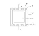
- FIG. 1 is a plan view showing a mounting surface of the camera module.
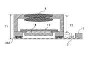
- FIG. 2 is a cross-sectional view taken along the cutting line II-II shown in FIG.
- FIG. 3 is a plan view showing a unit area of the film structure.
- FIG. 4 is a cross-sectional view taken along the cutting line IV-IV shown in FIG.
- FIG. 5 is a cross-sectional view showing a sticking process of sticking the connection film to the camera module.
- FIG. 6 is a cross-sectional view showing a state in which the base material is peeled off from the connecting film in the sticking step.
- FIG. 7 is a cross-sectional view showing a mounting process for mounting the flexible substrate on the camera module.
- FIG. 8 is a cross-sectional view showing a connection process for connecting the terminals of the camera module and the terminals of the flexible substrate via the connection film.
- FIG. 9 is a cross-sectional view showing a connection structure in which a camera module is mounted.
- FIG. 10 is a cross-sectional view showing a configuration example of a connection structure in which a camera module is mounted.
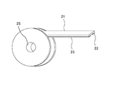
- FIG. 11 is a perspective view showing a film wound body.
- FIG. 12 is a plan view showing the film structure of the modified example 1.
- FIG. 13 is a plan view showing the film structure of the modified example 2.
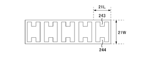
- FIG. 14 is a plan view showing the film structure of the modified example 3.
- FIG. 15 is a plan view showing the film structure of the modified example 4.
- FIG. 12 is a plan view showing the film structure of the modified example 1.
- FIG. 16 is a plan view showing a mounting surface of another example of the camera module.
- FIG. 17 is a plan view showing a first example of the film structure corresponding to the mounting surface shown in FIG.
- FIG. 18 is a plan view showing a second example of the film structure corresponding to the mounting surface shown in FIG.
- FIG. 19 is a plan view showing a third example of the film structure corresponding to the mounting surface shown in FIG.
- FIG. 20 is a plan view showing an example of a mounting surface of the camera module according to another embodiment.
- FIG. 21 is a plan view showing an example of a connection film corresponding to the mounting surface of the camera module shown in FIG.
- FIG. 22 is a perspective view showing an example of a tape-shaped film structure around which the connection film shown in FIG. 21 is wound.
- FIG. 23 is a cross-sectional view in the width direction including the non-attached portion of the film structure.
- connection structure 2. Connection structure 3. Film structure 4. Method for manufacturing a film structure 5. Modification example 6. Example
- the method for producing a connection structure according to the present embodiment is a method of manufacturing a connection structure according to a predetermined length in the length direction of the base material from a film structure including a tape-shaped base material and a connection film formed on the base material.
- the connecting film can be stuck at once without sticking the connecting film a plurality of times corresponding to a plurality of terminal rows.
- the "unit region” has a predetermined length in the length direction of the base material, and indicates, for example, a rectangular region.
- the “non-sticking portion” indicates a region in which the connecting film is not stuck to the electronic component in the unit area, and examples thereof include a gap in which the connecting film does not exist, a connecting film that is not stuck by cutting.
- the mounting surface is composed of a plurality of convex portions, the convex portion has a terminal row, the flat mounting surface has a plurality of terminal rows, and the mounting surface has a concave portion in the center.
- a terminal row is formed on the peripheral edge of the mounting surface.
- the first electronic component having a recess in the center of the mounting surface has, for example, a rectangular mounting surface, and the mounting surface has two opposing sides, two adjacent sides (L-shaped), or an adjacent peripheral edge of the recess. Some have terminal rows on three sides (U-shaped, U-shaped, and C-shaped) on the periphery of the recess. Further, the terminal row may be provided on the entire circumference of the peripheral edge.
- the peripheral edge of these recesses and the terminal row may be configured only in parallel or vertical, but the present invention is not limited to this, and is appropriately adjusted depending on the object. Therefore, the shape of the unit region of the connecting film is also adjusted accordingly.
- the outer shape of the mounting surface is not limited to a rectangular shape, but may be, for example, a curved shape, a circular shape, a polygonal shape, or the like. Further, the outer shape of the mounting surface may be composed of sides as described above, or may have a shape in which the inside is removed (extracted). Further, the shape of the mounting component having the mounting surface may or may not be the same as the shape of the mounting surface. This may be either one or both of the first electronic component and the second electronic component (not shown).
- the film structure When the first electronic component has a recess in the center of the mounting surface, the film structure preferably has a non-sticking portion in the direction from the peripheral edge of the unit region to the center of the unit region. This makes it possible to prevent the recess from being filled with gas and reducing the reliability of the connection.
- the non-attached portion is formed from the central portion of at least one side of the unit region toward the central portion of the unit region.
- the first electronic component having a mounting surface on which terminal rows are formed on three sides (U-shaped) of the peripheral edge of the recess.
- the non-attached portion is formed in the unit region from the central portion in the width direction of the base material in the length direction of the base material. As a result, it is possible to mount the first electronic component having a mounting surface on which terminal rows are formed on two opposite sides of the peripheral edge of the recess.
- the connecting film is linearly processed to form a polygonal shape such as a hexagon, an octagon, or a dodecagon, a U-shape, or a U-shape consisting of a curved line.
- C-shaped or cylindrical pasting portion may be used.
- the sticking portion of the connecting film may have a shape in which straight lines and curved lines are mixed.
- the polygonal shape may be a regular polygon. Further, the corners of these shapes may be chamfered. Further, the sticking portion of the connection film may have a shape in which a part thereof is lost.
- the corner portion of the rectangle may be deleted, and the attachment portion of the connecting film may have a cross shape or a similar shape.
- the corners of the rectangular connecting film may be chamfered with a straight line to form a non-attached portion, and the attached portion may be octagonal.
- Each corner of the square or rectangular connecting film can be linearly chamfered to form an octagon, or the square or rectangular connecting film can be cut off to form a cross. As a result, it is possible to mount the connecting film in an octagonal or cross shape.
- the chamfering process and the defect processing are not limited to a straight line, and may be a curved line or a shape in which a straight line and a curved line are mixed.
- the octagonal or cross-shaped connecting film is an example, and only a part of the connecting film may be chamfered or chipped.
- the connection film may have a shape in which a part of the in-plane is removed (pulled out).
- the shape of the connecting film is not limited to a straight line as described above, and may be a curved line or a shape in which a straight line and a curved line are mixed. In this case, as the film structure, only the connecting film may be removed, or the connecting film and the base material may be removed.
- the more precise and compact the shape the more preferably the shape is chamfered or chipped (punched).
- the attachment portion of the connection film may be, for example, a rectangular shape, a curved shape, a circular shape, a polygonal shape, or the like according to the shape of the mounting surface, and a part of these shapes is missing. It may be a U-shape, a U-shape, a C-shape, or the like. Further, the sticking portion of the connection film may have a hollowed-out shape with a part in the surface removed.
- connection film By matching the shape of the sticking part of the connection film to the outer shape of the mounting surface, it is possible to prevent a part of the connecting film from protruding excessively from the mounting surface, which facilitates the handling of the electronic components to be mounted and improves workability. It can be improved, prevented from interfering with the pre- and post-processes, and thus the overall manufacturing cost can be reduced.
- the connection in the process of bonding the connection film to the substrate (temporary application), since the outer shapes of the substrate and the connection film are close to each other, the effect of improving workability can be expected.
- the size of the outer peripheral edge of the sticking portion in the unit region may be smaller or the same as the size of the outer peripheral edge of the mounting surface of the first electronic component or the second electronic component. , May be large.
- the lower limit of the size of the outer peripheral edge of the sticking portion with respect to the size of the outer peripheral edge of the mounting surface is preferably 50% or more, and more preferably 80% or more.
- the upper limit for the size of the outer peripheral edge of the mounting surface should be 110% or less because if it is too small, it is desirable that there is a margin for stable pasting when mounting is continuously performed. Is more preferable, 105% or less is more preferable, and 100% or less is more preferable.
- the size of the sticking portion may be adjusted in consideration of the effective connection area and the influence of the protrusion. It is preferable that the outer peripheral edge of the sticking portion and the mounting surface of the first electronic component or the second electronic component have the same or similar shapes, but even if there are some differences, this book It is not excluded from the scope of technology.
- the film structure has a non-sticking portion at the center in the unit region.
- the non-sticking portion may have a hollow shape with a part in the surface removed. That is, in the film structure, the sticking portion has an outer peripheral edge and an inner peripheral edge in the unit region.
- the attachment portion of the connection film is required to have a sufficient effective connection area between the outer peripheral edge and the inner peripheral edge.
- the non-attached portion may be a slit or a hole portion.
- the U-shaped shape, the U-shaped shape, and the C-shaped shape do not necessarily have to be connected. In this way, since it may be composed of sides, all the sides forming the outer shape may be connected and may have a hollow shape.
- a film structure may be formed by providing a sticking portion on the base material so that the portions corresponding to the sides constituting these shapes are separated from each other. In the process of temporarily pasting the connection film and the process of connecting, the workability is improved if it is performed collectively, and the introduction cost can be suppressed because the improvement of the equipment and equipment can be reduced if it is performed for each side.
- the connecting film (pasting part) on such a side is arranged on the base material, the film winding body to be pulled out can be accommodated by one, and the improvement from the existing manufacturing equipment can be made. It is expected that it will be relatively small. The same effect can be expected even if all the sides forming the outer shape are connected and the shape is hollowed out. It may be appropriately selected depending on the conditions such as temporary attachment of the connection film and restrictions on equipment improvement for crimping.
- the first electronic component and the second electronic component are not particularly limited and can be appropriately selected according to the purpose.
- the first electronic component include a ceramic substrate, a rigid substrate, a flexible substrate (FPC: Flexible Printed Circuits), a glass substrate, a plastic substrate, a resin multilayer substrate, an IC (Integrated Circuit) module, an IC chip, and the like.
- the second electronic component include a ceramic substrate, a rigid substrate, a flexible substrate (FPC: Flexible Printed Circuits), a glass substrate, a plastic substrate, a resin multilayer substrate, and the like.
- a ceramic substrate may be used from the viewpoint of excellent electrical insulation and thermal insulation.
- the ceramic substrate has advantages such as excellent dimensional stability in miniaturization (for example, 1 cm 2 or less).
- the connecting film is not particularly limited, and examples thereof include a film-like anisotropic conductive film (ACF: Anisotropic Conductive Film) and a film-like adhesive film (NCF: Non Conductive Film).
- the curable type of the connection film is not particularly limited, and examples thereof include a thermosetting type, a photocuring type, and a photocuring combined type. Further, the connecting film may be a hot melt type using a thermoplastic resin.
- the connection film according to the present technology is provided on a base material (base material film) and is separable from the release film. It is different from the one that uses an adhesive or a curable resin as an integral part of the base material (uses without separation). Therefore, advanced processing technology for connecting films is required.
- this technology includes, for example, semiconductor devices (including driver ICs, optical elements, thermoelectric conversion elements, photoelectric conversion elements, and other devices that use semiconductors), display devices (monitors, televisions, head mount displays, etc.), Portable devices (tablet terminals, smartphones, wearable terminals, etc.), game machines, audio devices, imaging devices (those that use image sensors such as camera modules), electrical equipment mounting for vehicles (mobile devices), medical devices, sensor devices (touch sensors) , Fingerprint authentication, iris authentication, etc.), and can be used in any method of manufacturing electronic devices that use electrical connections such as home appliances.
- semiconductor devices including driver ICs, optical elements, thermoelectric conversion elements, photoelectric conversion elements, and other devices that use semiconductors
- display devices monitors, televisions, head mount displays, etc.
- Portable devices tablet terminals, smartphones, wearable terminals, etc.
- game machines audio devices
- imaging devices such as camera modules
- electrical equipment mounting for vehicles mobile devices
- medical devices sensor devices (touch sensors) , Fingerprint authentication, iris authentication, etc.
- connection structure for mounting a camera module
- the manufacturing method of the connection structure shown as a specific example includes a sticking process of sticking a connecting film to the camera module, a mounting process of mounting a flexible substrate on the camera module, and terminals of the camera module and terminals of the flexible substrate via the connecting film. It has a connection process for connecting to and.
- FIG. 1 is a plan view showing a mounting surface of a camera module
- FIG. 2 is a cross-sectional view taken along the cutting line II-II shown in FIG.
- the camera module 10 has a ceramic substrate 11 having a concave portion (cavity) on a rectangular mounting surface, and a second portion formed on the rectangular mounting surface on two opposite sides of the peripheral edge of the concave portion. It includes a terminal row 12 of 1, a second terminal row 13, and an image sensor 14 housed in a recess.
- the camera module 10 has a mounting surface having a predetermined width of 12 W on which the first terminal row 12 is formed and a mounting surface having a predetermined width of 13 W on which the second terminal row 13 is formed.
- FIG. 3 is a plan view showing a unit region of the film structure
- FIG. 4 is a cross-sectional view taken along the cutting line IV-IV shown in FIG.
- the film structure 20 includes a tape-shaped base material 21 and connecting films 22 and 23 formed on the base material 21, and the length of the base material 21 in a plan view. It has a rectangular unit region having a predetermined length of 21 L in the direction and a predetermined width of 21 W in the width direction of the base material 21.
- the film structure 20 has a void 24 which is a non-attached portion in the length direction of the base material 21 from the central portion in the width direction of the base material 21 in the unit region.
- the void 24 can be formed, for example, by removing an adhesive film from the central portion in the width direction of the base material 21 in the length direction of the base material 21. That is, in the film structure 20, the non-attached portion is formed in the unit region from the central portion in the width direction of the base material in the length direction of the base material, and the first terminal row 12 and the first terminal row 12 of the ceramic substrate 11 and the first A connection film 22 having a predetermined width of 22 W and a connection film 23 having a predetermined width of 23 W are formed apart from each other in the length direction of the base material 21 corresponding to the terminal row 13 of 2.
- the width 22W of the connection film 22 and the width 23W of the connection film 23 are the same even if they are narrower than the width 12W of the mounting surface of the first terminal row 12 and the width 13W of the mounting surface of the second terminal row 13, respectively. But it can be wide.
- the width of the connecting film is narrower than the width of the mounting surface of the terminal row, it is possible to suppress excessive protrusion of the resin of the connecting film from the film connector. Therefore, it is possible to prevent the excessively protruding resin from coming into contact with the camera module and other mounted parts, and it is possible to improve the workability of assembly. It is also effective when it is preferable to avoid contamination of the mounted components.
- the width of the connection film is wider than the width of the mounting surface of the terminal row, a sufficient amount of resin can be secured for the connection portion, so that the peel strength (connection strength) of the object to be connected can be improved. This is effective when you want to secure sufficient connection strength for the connection structure.
- the width of the connecting film is the same as the width of the mounting surface of the terminal row, the above two advantages can be combined.
- the width of the connection film and the width of the mounting surface of the terminal row may be appropriately adjusted according to the specifications required for the mounting portion.
- the lower limits of the width 22W of the connection film 22 and the width 23W of the connection film 23 are the width 12W of the mounting surface of the first terminal row 12 and the width of the second terminal row, respectively. It is preferably 80% or more, more preferably 100% or more, and even more preferably 120% or more of the width 13W of the mounting surface of 13. From the viewpoint of shape processing, if it is too narrow, the difficulty level increases. Therefore, as an example, the width is 0.3 mm or more, preferably 0.4 mm or more, and more preferably 0.5 mm or more.
- the upper limits of the width 22W of the connection film 22 and the width 23W of the connection film 23 are 280% or less of the width 12W of the mounting surface of the first terminal row 12 and the width 13W of the mounting surface of the second terminal row 13, respectively. It is preferably present, and more preferably 240% or less.
- the lower limit of the width 24W of the gap 24 is 5% or more, preferably 10% or more, more preferably 20% or more with respect to the width 21W of the base material 21, and the upper limit of the width 24W of the gap 24 is the base material. It is 80% or less, preferably 75% or less, and more preferably 60% or less with respect to the width 21W of 21. If the width 24W of the gap 24 is too small, there is a concern that the recesses will be sealed due to the resin flow, and if the width 24W of the gap 24 is too large, the width of the connecting film will be narrowed. In some cases, there is a concern that the adhesive strength of the connecting body may not be satisfactory.
- the width 24W of the gap 24 is preferably 1.0 mm or more, and preferably 1.2 mm or more.
- the width 24W of the gap 24 is preferably 1.0 mm or more, and preferably 1.2 mm or more.
- FIG. 5 is a cross-sectional view showing a sticking process of sticking the connection film to the camera module
- FIG. 6 is a cross-sectional view showing a state in which the base material is peeled off from the connecting film in the sticking step.
- the connecting films 22 and 23 of the unit region of the film structure 20 are transferred to the camera module 10.
- the film structure is pressed from the base material side, and the connecting films 22 and 23 of the unit area are collectively stuck on the mounting surface of the camera module 10 on the stage.
- the film structure to which the connecting films 22 and 23 are transferred is wound up as only the base material.
- FIG. 7 is a cross-sectional view showing a mounting process for mounting the flexible substrate on the camera module.
- the flexible substrate 30 corresponds to the first terminal row 12 and the second terminal row 13 of the camera module 10 and corresponds to the first terminal row 32 and the second terminal row 32 on the base material 31. It has row 33.
- the first terminal row 32 and the second terminal row 33 of the flexible substrate 30 and the first terminal row 12 and the second terminal row 13 of the camera module 10 are aligned with each other in the camera module 10.
- the flexible substrate 30 is mounted.
- FIG. 8 is a cross-sectional view showing a connection process for connecting the terminals of the camera module and the terminals of the flexible substrate via the connection film.
- the connection step for example, the first terminal row 12 of the camera module 10 and the first terminal row 32 of the flexible substrate 31 are pressed by the crimping tool 42 via the cushioning material 41.
- the second terminal row 13 of the camera module 10 and the second terminal row 33 of the flexible substrate 30 are pressed by the crimping tool 43.
- heating, light irradiation, or the like is performed to cure the connecting film.
- FIG. 9 is a cross-sectional view showing a connection structure in which a camera module is mounted.
- the first terminal row 12 of the camera module 10 and the first terminal row 32 of the flexible substrate 30 are the cured film 22A in which the connection film 22 is cured.
- the second terminal row 13 of the camera module 10 and the second terminal row 33 of the flexible substrate 30 are connected by a cured film 23A obtained by curing the connection film 23.
- the cured film 23 is a cured film connected by a hot-melt type connecting film.
- the film structure has a non-sticking portion in the direction from the peripheral portion of the unit region to the central portion of the unit region in a plan view, so that the existing equipment can be used.
- An electronic component having a recess in the center of the mounting surface can be mounted, and it is possible to prevent the recess from being filled with gas and deteriorating reliability.
- connection structure has a first electronic component having a recess in the center of the mounting surface, a second electronic component, and between the first electronic component and the second electronic component.
- a cured film obtained by curing a connecting film having a non-attached portion in the direction from the peripheral edge portion of the unit region having a predetermined length and a predetermined width to the central portion of the unit region in a plan view is provided, and the terminal of the first electronic component and the second It is connected to the terminals of the electronic components of.
- the first electronic component and the second electronic component are not particularly limited and can be appropriately selected according to the purpose.
- the connecting film and the curable type of the connecting film are not particularly limited and may be appropriately selected depending on the intended purpose.
- FIG. 10 is a cross-sectional view showing a configuration example of a connection structure in which a camera module is mounted.
- the connection structure is a flexible structure having a camera module 10 having a first terminal row 12 and a second terminal row 13, and a first terminal row 32 and a second terminal row 33. Between the substrate 30, the first terminal row 12 and the first terminal row 32, the cured film 22A on which the connection film 22 is cured, and between the second terminal row 13 and the second terminal row 33.
- connection structure has a protective glass 15 fixed on the ceramic substrate 11 and a lens 16 arranged on the image sensor 14 and installed in the housing.
- camera module driving IC 17 may be mounted on the flexible substrate 30 in addition to the camera module mounting portion.
- connection structure having such a configuration, it is difficult to optically shorten the distance T2 between the image sensor 14 and the lens 16, but the distance T1 between the lens 16 and the flexible substrate 30 Can be shortened and can be made thinner. Further, in the connection structure, on the rectangular mounting surface, two opposing sides of the peripheral edge of the concave portion of the ceramic substrate 11 are fixed by the cured film 22A and the cured film 23A, and a part of the other two sides is not fixed. Therefore, it is possible to prevent the concave portion of the ceramic substrate 11 from being closed by the base material 31 of the flexible substrate 30 and the flexible substrate 30 from swelling due to the influence of gas.
- the film structure according to the present embodiment includes a tape-shaped base material and a connecting film formed on the base material, and has a unit region having a predetermined length in the length direction of the base material in a plan view. , It has a non-sticking portion in the direction from the peripheral portion of the unit region to the central portion of the unit region. Further, the film structure can be in the form of a film wound body wound around a winding core.
- FIG. 11 is a perspective view schematically showing the film winding body.
- the film winding body is formed by winding a film structure including a tape-shaped base material 21 and connecting films 22 and 23 formed on the base material 21 around a winding core 25. ..
- the winding core 25 has a shaft hole into which a rotating shaft for rotating the reel is inserted, and connects one end of the film structure in the longitudinal direction to wind the film structure.
- the length of the film structure wound around the film winding body is not particularly limited, but the lower limit of the length is 5 m or more, 10 m or more, 50 m or more, and the upper limit of the length is 5000 m or less. Those having a length of 3000 m or less and 1000 m or less can be preferably used.
- the base material 21 is a support film that is molded into a tape shape and supports the connection films 22 and 24.
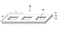
- Examples of the base material 21 include PET (PolyEthylene Terephthalate), OPP (Oriented Polypropylene), PMP (Poly-4-methylpentene-1), and PTFE (Polytetrafluoroethylene).
- PET PolyEthylene Terephthalate
- OPP Oriented Polypropylene
- PMP Poly-4-methylpentene-1
- PTFE Polytetrafluoroethylene
- at least the surfaces of the connecting films 22 and 23 are preferably peeled off with, for example, a silicone resin.
- the thickness of the base material is not particularly limited.
- the lower limit of the thickness of the base material is preferably 10 ⁇ m or more, more preferably 25 ⁇ m or more, and even more preferably 38 ⁇ m or more for separation.
- the upper limit of the thickness of the base material is preferably 200 ⁇ m or less, more preferably 100 ⁇ m or less, and more preferably 75 ⁇ m or less because there is a concern that excessive pressure is applied to the connecting film if it is too thick. Even more preferable. It may be 50 ⁇ m or less. Further, in the present technology, since it is assumed that the base material and the connecting film can be separated, it is not preferable that the unit region is extremely small because unnecessary separation occurs. Further, it is not preferable that the gap portion is too large for the same reason.
- the width of the base material is not particularly limited.
- the lower limit of the width of the base material is preferably 1 mm or more, more preferably 2 mm or more, and even more preferably 4 mm or more in winding. If the upper limit of the width of the base material is too large, there is a concern that it will be difficult to carry and handle. Therefore, it may be 250 mm or less, preferably 120 mm or less, more preferably 60 mm or less, and 10 mm or less. It is even more preferable to have.
- the width of the base material may be appropriately adjusted from the size of the unit region and the void portion. From the viewpoint of productivity, it is preferable that a part of the connecting film is in contact with the end of the width of the base film.
- connection film and the curable type of the connection film are not particularly limited and can be appropriately selected according to the purpose.
- the cured type may be replaced with a hot melt type.
- the lower limit of the thickness of the anisotropic conductive film may be, for example, the same as the conductive particle diameter, and preferably 1.3 times or more or 10 ⁇ m or more of the conductive particle diameter.
- the upper limit of the thickness of the anisotropic conductive film can be, for example, 40 ⁇ m or less or twice or less the diameter of the conductive particles.
- the anisotropic conductive film may be laminated with an adhesive layer or an adhesive layer that does not contain conductive particles, and the number of layers and the laminated surface can be appropriately selected according to the target and the purpose. ..
- the adhesive layer and the insulating resin of the adhesive layer the same one as that of the anisotropic conductive film can be used.
- the conductive particles may be dispersed in the resin or may be arranged. Further, when the conductive particles are dispersed in the resin, they may be individually separated from each other in a non-contact manner.
- the anisotropic conductive film preferably contains the conductive particles so that the number of captured conductive particles per terminal is preferably 5 or more, more preferably 10 or more.
- conductive particles those used in known anisotropic conductive films can be appropriately selected and used.
- metal-coated resin particles in which the surface of metal particles such as nickel, copper, silver, gold, and palladium, and resin particles such as polyamide and polybenzoguanamine are coated with a metal such as nickel can be mentioned.
- the surface may be insulated to the extent that the conduction performance is not impaired. Further, the surface shape may have protrusions.
- the particle size of the conductive particles is not particularly limited, but the lower limit of the particle size is preferably 2 ⁇ m or more, and the upper limit of the particle size is, for example, 50 ⁇ m or less from the viewpoint of the capture efficiency of the conductive particles in the connection structure. It is preferably 20 ⁇ m or less, and more preferably 20 ⁇ m or less.
- the particle size of the conductive particles can be a value measured by an image-type particle size distribution meter (for example, FPIA-3000: manufactured by Malvern). The number is preferably 1000 or more, preferably 2000 or more.
- the insulating binder As the insulating binder (insulating resin), a known insulating binder can be used.
- the curing type include a thermosetting type, a photocuring type, and a photocuring combined curing type.
- a photoradical polymerization type resin composition containing a (meth) acrylate compound and a photoradical polymerization initiator a thermal radical polymerization type resin composition containing a (meth) acrylate compound and a thermal radical polymerization initiator, an epoxy compound and heat.
- examples thereof include a thermal cationic polymerization type resin composition containing a cationic polymerization initiator, a thermal anionic polymerization type resin composition containing an epoxy compound and a thermal anionic polymerization initiator, and the like.
- thermal radical polymerization type insulating binder containing a film-forming resin, an elastomer, a (meth) acrylic monomer, a polymerization initiator, and a silane coupling agent
- the (meth) acrylic monomer means to include both an acrylic monomer and a methacrylic monomer.
- the film-forming resin is not particularly limited, and examples thereof include phenoxy resin, unsaturated polyester resin, saturated polyester resin, urethane resin, butadiene resin, polyimide resin, polyamide resin, and polyolefin resin.
- the film-forming resin may be used alone or in combination of two or more. Among these, it is particularly preferable to use a phenoxy resin from the viewpoint of film forming property, processability, and connection reliability.
- the phenoxy resin is a resin synthesized from bisphenol A and epichlorohydrin, and an appropriately synthesized resin may be used, or a commercially available product may be used.
- the content of the film-forming resin is not particularly limited, and is preferably, for example, 10% by mass to 60% by mass.
- the elastomer is not particularly limited, and examples thereof include polyurethane resin (polyurethane-based elastomer), acrylic rubber, silicone rubber, and butadiene rubber.
- the (meth) acrylic monomer is not particularly limited, and may be, for example, a monofunctional (meth) acrylic monomer or a bifunctional or higher polyfunctional (meth) acrylic monomer. From the viewpoint of stress relaxation of the polymer, it is preferable that 80% by mass or more of the (meth) acrylic monomer in the insulating binder is a monofunctional (meth) acrylic monomer.
- the monofunctional (meth) acrylic monomer preferably has a carboxylic acid.
- the molecular weight of the monofunctional (meth) acrylic monomer having a carboxylic acid is preferably 100 to 500, and more preferably 200 to 350.
- the content of the monofunctional (meth) acrylic monomer having a carboxylic acid in the insulating binder is preferably 3% by mass to 20% by mass, and more preferably 5% by mass to 10% by mass.
- the polymerization initiator is not particularly limited as long as it can cure the (meth) acrylic monomer at a predetermined temperature during thermocompression bonding, and examples thereof include organic peroxides.
- examples of the organic peroxide include lauroyl peroxide, butyl peroxide, benzyl peroxide, dilauroyl peroxide, dibutyl peroxide, peroxydicarbonate, and benzoyl peroxide. These may be used alone or in combination of two or more.
- the content of the polymerization initiator in the insulating binder is not particularly limited, and is preferably, for example, 0.5% by mass to 15% by mass.
- the silane coupling agent is not particularly limited, and examples thereof include an epoxy-based silane coupling agent, an acrylic-based silane coupling agent, a thiol-based silane coupling agent, and an amine-based silane coupling agent.
- the content of the silane coupling agent in the insulating binder is not particularly limited, and is preferably 0.1% by mass to 5.0% by mass, for example.
- the method for producing a film structure includes a processing step of processing a film raw fabric including a tape-shaped base material and a connecting film formed on the base material.
- the length of the base material in a plan view is obtained.
- a film structure having a unit region having a predetermined length in the longitudinal direction and a predetermined width in the width direction of the base material and having a non-sticking portion in the direction from the peripheral portion of the unit region to the central portion of the unit region is formed.
- a connecting film having a desired shape is formed in a unit region by slitting, half-cut punching, punching, punch pressing, or the like on the original film.
- the connecting film on the base film may be processed and removed. Further, a step of providing the cover film on the surface of the connecting film may be provided. Therefore, the cover film may be used as a support (substitute for the base material), and the base material and the connecting film may be subjected to the above processing. As described above, since the base material and the connecting film are peeled (separated) from the base material during use, the degree of difficulty of the processing technique is high.
- the material of the cover film may be the same as that of the base material 21 described above. The thickness is preferably thinner than that of the base material 21.
- the film structure shown in FIGS. 3 and 4 is fully cut so as to have a unit region having a predetermined width in a plan view, and is oriented from the peripheral portion of the unit region to the central portion of the unit region. It can be obtained by performing a half cut so as to have a non-attached portion. Specifically, it can be obtained by fully cutting the original film with a width of 21 W in the unit region, half-cutting with a width of 24 W that becomes a gap 24, and punching a connecting film having a width of 24 W.
- the connecting film is punched out from the film structure, the resin of the connecting film can move to the voids that are not attached, so it is possible to suppress the protrusion and blocking that occur when the film is made into a reel.
- This has the advantage of increasing the degree of freedom in compounding design as a connecting film.
- the connection film and the processed portion may come into contact with each other, leaving traces of processing on the connecting film, which may be unfavorable in appearance.
- a cover film may be provided to prevent this.
- the half-cut depth is preferably 1% or more and 95% or less of the thickness of the base material.
- the resin of the connecting film that sticks out enters the half-cut portion, so that sticking out and blocking can be suppressed.
- the depth of the half cut is preferably 5% or more of the thickness of the base material. This is due to the thickness of the base material, but it is more preferably 10% or more in order to perform a stable half cut.
- the viscosity of the adhesive film is high, it is preferably larger than 50%, more preferably 55% or more, and even more preferably 60% or more in order to obtain a reliable cut product.
- the half-cut depth is 90% of the thickness of the base material. It is preferably less than or equal to, more preferably 80% or less, further preferably 50% or less, and in some cases preferably 25% or less. This may be appropriately selected depending on the thickness of the base material and the film length. In addition, such a half-cut makes it easier to remove the connecting film from the base material, which is expected to improve the manufacturing productivity of the connecting structure.
- the processed film structure may be left in a state where the connecting film provided on one surface is half-cut, and by removing a part of the connecting film, the connecting films are individually present on the base material. May be good. Further, from the viewpoint of manufacturing, it is preferable that the connecting film is supported on the base material, but the base material may be removed by using the cover film as a support.
- the film structure may be selected in consideration of overall workability and economy from the manufacturing process of the film structure to the connecting process using the film structure. With such a wide range of choices, convenience is enhanced.
- Modification example> 12 to 15 are plan views showing the film structures of the modified examples 1 to 4, respectively.
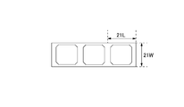
- the gap 241 which is a non-sticking portion is formed in the unit region from the central portion of the two sides in the length direction of the base material to the entire width direction of the base material. It can be used for electronic components having a recess in the center of a rectangular mounting surface and terminal rows on two opposite sides of the periphery of the recess.
- the gap 242 which is a non-attached portion, is a part in the width direction of the base material from the central portion of one side in the length direction of the base material in the unit region. It is possible to deal with electronic components having a recess in the center of a rectangular mounting surface and terminal rows on three sides of the periphery of the recess.
- the gaps 243 and 244 which are non-attached portions, are in the unit region from the central portion of the two sides in the length direction of the base material to the width direction of the base material. It can be used for electronic components that are partially formed, have a recess in the center of a rectangular mounting surface, and have terminal rows on two opposite sides of the peripheral edge of the recess.
- the film structures of such modified examples 1 to 3 can be formed by, for example, punching.
- the gap 245, which is a non-attached portion is a part in the width direction of the base material from the central portion of one side in the length direction of the base material in the unit region. It is possible to deal with electronic components having a recess in the center of a rectangular mounting surface and terminal rows on three sides of the periphery of the recess.
- the film structure of the modified example 4 is a simple one in which neither a base material nor a connecting film exists in the non-attached portion by punch press processing, for example, and the connecting film is connected by an existing attaching device with a unit area length of 21 L. Can be half-cut.
- FIG. 16 is a plan view showing the mounting surface of the camera module.
- the camera module 50 has a ceramic substrate 51 having a concave portion (cavity) on a rectangular mounting surface, and a first terminal row formed on two opposite sides of the concave edge on the rectangular mounting surface. 52, the second terminal row 53, and the third terminal row 54 formed on one of the two sides that do not touch the two sides on which the first terminal row 52 and the second terminal row 53 are formed. It includes an image sensor 55 housed in a recess.
- the mounting surface of the camera module 50 is rectangular, has a recess in the center, and has terminal rows on three sides (U-shaped) of the periphery of the recess.
- FIG. 17 is a plan view showing a first example of a film structure corresponding to the mounting surface shown in FIG.
- the film structure shown in FIG. 17 has an octagonal shape at the periphery of the sticking portion in the unit areas 21L and 21W.
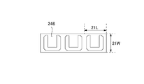
- FIG. 18 is a plan view showing a second example of the film structure corresponding to the mounting surface shown in FIG.
- the gap 246, which is a non-sticking portion is formed in the width direction of the base material from the center of one side in the length direction of the base material. It was formed as a part of.
- FIG. 19 is a plan view showing a third example of the film structure corresponding to the mounting surface shown in FIG.
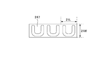
- the film structure shown in FIG. 19 has a U-shape in the unit regions 21L and 21W in which the shape of the peripheral edge of the sticking portion corresponds to the mounting surface shown in FIG.
- the corners of the rectangular sticking portion are processed with a curved line, and the void 247, which is a non-sticking portion, is formed from the center of one side in the length direction of the base material to a part in the width direction of the base material.
- the corner portion is chamfered in a curved shape to form a U-shaped pasting portion.
- the film structure shown as the first to third examples is, for example, a blade for cutting a base film (for example, polyethylene terephthalate) which is a base material, and a connecting film cut into each shape, and about half the thickness of the base material. It can be obtained by producing a master with a half-cut blade that penetrates, punching the film raw fabric using this master, and removing the non-attached portion. Further, the master may have a connecting portion. In this case, in the longitudinal direction of the film structure, there may be a portion where the distance between the sticking portions of the connecting film is partially different, but this is advantageous in terms of manufacturing control such as number counting.
- a method for producing a connection structure is based on a film structure including a tape-shaped base material, a connection film formed on the base material, and a cover film attached on the connection film.
- a connecting film having a unit region having a predetermined length in the length direction of the material and a predetermined width in the width direction of the base material is applied to a substrate component having an element and a plurality of electrodes formed around the element or an electrode of the substrate component. It has a sticking step of sticking to an electronic component having a corresponding electrode and a connecting step of connecting the electrode of the substrate component and the electrode of the electronic component via a connecting film, and the film structure is the element in a unit region.
- the non-attached part is made of a cover film at the corresponding part. Since the non-attached part is made of a cover film, when the film structure is wound around the winding core, it comes into contact with the resin-processed base material of the adhesive film, and the shape is reflected in the appearance. Can be prevented from worsening. In addition, it is possible to prevent the resin from excessively protruding into the voids.
- cover film for example, PET, OPP, PMP, PTFE and the like can be used in the same manner as the base material.
- the thickness of the cover film is preferably thinner than that of the base material, preferably 8 to 38 ⁇ m, and more preferably 12 to 25 ⁇ m.
- connection film it is preferable to align the connection film and stick it to the substrate component or the electronic component. As a result, it is possible to reliably prevent the adhesive film from adhering to the element.
- connection structure includes a substrate component including an element and a plurality of electrodes formed around the element, an electronic component including electrodes corresponding to the electrodes of the substrate component, and a substrate component.
- a cured film obtained by curing a connection film in which the element portion is a gap is provided between the substrate component and the electronic component in a unit region having a predetermined length and a predetermined width, and the electrode of the substrate component and the electrode of the electronic component are connected to each other. Being done.
- a connection film in which the portion of the element is a gap, it is possible to prevent the adhesive film from adhering to the element and deteriorating the function of the element.
- the connection film can be temporarily attached to the substrate while avoiding the elements, the work efficiency during the connection process is improved. Since such an element is often relatively expensive, it can be said that processing the connection film structure in advance is highly economical from a comprehensive point of view.
- the board parts and electronic parts are not particularly limited and can be appropriately selected according to the purpose.
- the substrate component include a ceramic substrate, a rigid substrate, a flexible substrate (FPC: Flexible Printed Circuits), a glass substrate, a plastic substrate, a resin multilayer substrate, an IC (Integrated Circuit) module, an IC chip, and the like.
- electronic components include ceramic substrates, rigid substrates, flexible substrates (FPCs: Flexible Printed Circuits), glass substrates, plastic substrates, resin multilayer substrates, and the like.
- a substrate component it can be applied to, for example, a semiconductor element provided in the center of a mounting surface and an electrode formed in a peripheral portion of the mounting surface.
- a substrate component having a semiconductor element in the center of a rectangular mounting surface two opposing sides of the mounting surface, two adjacent sides (L-shaped), or three sides of the peripheral edge of the mounting surface (U-shaped) , U-shaped, C-shaped), or those having electrodes on four or all sides (when corresponding to a shape of pentagon or more).
- the connection film and the base material may be penetrated and hollowed out (the middle part of the surface is hollowed out).
- the outer shape of the mounting surface is not limited to a rectangular shape, but may be, for example, a curved shape, a circular shape, a polygonal shape, or the like.
- a camera module or the like in which an image sensor is mounted in the center of a ceramic substrate is suitable from the viewpoint of excellent electrical insulation and thermal insulation.
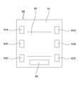
- FIG. 20 is a plan view showing an example of a mounting surface of the camera module according to another embodiment.
- the ceramic substrate 61, the first electrodes 62A, 62B, 62C formed on the two opposite sides of the peripheral edge of the image sensor 65, and the second electrodes 63A, 63B, respectively.
- the third electrode 64 formed on one of the two sides where the first electrodes 62A, 62B, 62C and the second electrodes 63A, 63B, 63C are not in contact with each other, and the ceramic substrate.
- It is provided with an image sensor 65 mounted in the central portion of 61. That is, the camera module 60 has first to third electrodes on three sides (U-shaped) of the peripheral edge of the rectangular image sensor 65.
- electrodes may be provided on all four sides of the peripheral edge of the image sensor.
- FIG. 21 is a plan view showing an example of a connection film corresponding to the mounting surface of the camera module shown in FIG. 20.
- the connection film 70 has a sticking portion 71 composed of four sides of the peripheral edge of the image sensor 65, and a non-sticking portion 72 in which the portion corresponding to the image sensor 65 is a hollow portion. Since the image sensor 65 portion is a gap portion, it is possible to prevent the connection film 40 from adhering to the image sensor 65.
- FIG. 22 is a perspective view showing an example of a tape-shaped film structure around which the connection film shown in FIG. 21 is wound
- FIG. 23 is a cross-sectional view in the width direction including a non-attached portion of the film structure.
- the film structure 80 includes a tape-shaped base material 81, a connecting film 82 formed on the base material 81, and a cover film 83 attached on the connecting film 82, in the length direction of the base material 81. It has a rectangular unit region having a predetermined length L and a predetermined width W in the width direction of the base material 81, and has a rectangular non-attached portion 84 made of a cover film 83 at the center of the unit region.
- the cover film 83 By attaching the cover film 83, even if the resin of the connecting film gets into the non-attached portion 84, the film structure can be easily pulled out from the wound body on which the film structure is wound. Further, by attaching the cover film 83, the appearance of the connecting film can be maintained.
- hollow portions in which the base material 81 and the connecting film 82 are punched are formed in each rectangular unit region having a predetermined length L and a predetermined width W.
- the cover film 83 of FIG. 22 does not penetrate, but the base material 81 and the connecting film 82 penetrate by punching.
- the connection film 82 may be half-cut or removed for each predetermined length L in order to accommodate the portion to be used. If the cover film is used as a support, the base material 81 and the connecting film 82 may be half-cut or removed at predetermined lengths L in order to suit the parts to be used. Further, the shape of FIG. 21 may be processed in advance and this may be attached to the cover film.
- the base material 81 and the cover film 83 are support films that are molded into a tape shape and support the connection film 82.
- Examples of the base material 81 and the cover film 83 include PET (PolyEthylene Terephthalate), OPP (Oriented Polypropylene), PMP (Poly-4-methylpentene-1), and PTFE (Polytetrafluoroethylene), as in the above-described embodiment. Can be mentioned.
- PET PolyEthylene Terephthalate
- OPP Oriented Polypropylene
- PMP Poly-4-methylpentene-1
- PTFE Polytetrafluoroethylene
- connection film 81 is not particularly limited as in the above-described embodiment, and examples thereof include a film-like anisotropic conductive film (ACF: Anisotropic Conductive Film) and a film-like adhesive film (NCF: Non Conductive Film). Be done.
- the curing type of the connection film 81 is also not particularly limited, and examples thereof include a thermosetting type, a photocuring type, and a photocuring combined type. Further, the connection film 81 may be a hot melt type using a thermoplastic resin.
- the film structure is wound around the winding core so that the cover film 83 is on the outside or inside.
- a film structure has a processing step of processing a film raw fabric including a tape-shaped base material and a connecting film formed on the base material, and affixing a cover film to the processed film raw material. It can be manufactured by punching a base material and a connecting film in a central portion in a unit region having a predetermined length in the length direction of the base material and a predetermined width in the width direction of the base material. it can. Further, if necessary, the film raw fabric can be fully cut to a predetermined width of the unit region, and these can be joined and wound around the winding core.
- the predetermined length and the predetermined width when punching the base material and the connecting film in the central portion of the unit region are, for example, 0.3 mm or more, preferably 0.4 mm or more, more preferably 0.5 mm or more. is there.
- the resin of the connecting film may protrude into the punched out portion and the non-attached portion may not be formed.
- the adhesive film is attached to the corresponding portion of the terminal row or the electrode, but the conductive particles may be provided only in the corresponding portion of the terminal row or the electrode.
- Examples of the technique for providing the conductive particles only in the corresponding portions of the terminal row and the electrode include JP-A-2016-119306 and JP-A-2016-131152.
- a resin mold in which recesses are arranged in a grid pattern at positions corresponding to terminal rows and electrodes, filling the recesses of the resin mold with conductive particles, and transferring the conductive particles from the resin mold to an insulating resin film.
- the conductive particles in the connecting film are preferably arranged so that the number of conductive particles captured by one terminal or electrode is five or more, and the conductive particles captured by one terminal or electrode are preferably arranged. It is even more preferable that the numbers are arranged so as to be 10 or more. Further, the arrangement of the conductive particles can be used as an alignment mark of the connecting film.
- connection structure was produced using an anisotropic conductive film, and the conduction characteristics were evaluated.
- a planetary agitator (product name) consisting of 5 parts by mass of resin core conductive particles (Ni (base) / Au (surface) plating, resin core) with an average particle size of 20 ⁇ m and 95 parts by mass of an insulating binder composed of the following components. : Awatori Rentaro, manufactured by THINKY Co., Ltd.) and stirred for 1 minute to prepare an anisotropic conductive adhesive composition. Then, the anisotropic conductive adhesive composition is applied onto a PET film having a thickness of 50 ⁇ m and dried in an oven at 80 ° C. for 5 minutes to form an adhesive layer composed of the anisotropic conductive adhesive composition on the PET film to form a width. An anisotropic conductive film having a thickness of 6.0 mm and a thickness of 25 ⁇ m was produced. The ratio of the conductive particles to the insulating binder was adjusted so that the number of captured particles after connection was 5 or more.
- the insulating binder is phenoxy resin (trade name: YP-50, manufactured by Shin Nikka Epoxy Manufacturing Co., Ltd.) 47 parts by mass, monofunctional monomer (trade name: M-5300, manufactured by Toa Synthetic Co., Ltd.) 3 parts by mass, urethane 25 parts by mass of resin (trade name: UR-1400, manufactured by Toyo Spinning Co., Ltd.), 15 parts by mass of rubber component (trade name: SG80H, manufactured by Nagase ChemteX Corporation), silane coupling agent (trade name: A-187, Contains 2 parts by mass of Momentive Performance Materials Japan) and 3 parts by mass of organic peroxide (trade name: Niper BW, manufactured by Nichiyu Co., Ltd.) so that the solid content is 50% by mass.
- a mixed solution of ethyl acetate and toluene was prepared.
- Thermocompression bonding was performed under the conditions of temperature: 120 ° C., pressure: 1 MPa, and time: 6 sec by pushing down the tool from the FPC side via a silicon rubber having a thickness of 200 ⁇ m. Practically, it is desirable to obtain 5 or more capture numbers at each terminal. When the indentation of the connection structure produced this time was observed with a microscope from the FPC side, it was confirmed that the number of conductive particles supplemented to the terminals was 5 or more.
- connection structure was subjected to a 90-degree peeling test on the FPC at a peeling speed of 50 mm / min, and the force required for peeling was measured.
- the adhesive properties were evaluated with the peel strength of Comparative Example 1 as 1.
- Example 1 An anisotropic conductive film having a width of 6.0 mm was attached to a substrate for evaluation of a camera module to prepare a connection structure.
- Table 1 shows the evaluation of the conduction characteristics and the adhesion characteristics of the connection structure.
- the thickness of the connecting film 22 is 50 ⁇ m so that the width of the connecting film 22 is 0.8 mm, the width of the connecting film 23 is 0.8 mm, and the width of the gap 24 is 4.4 mm.
- the PET film of No. 1 was half-cut to a depth of 20 ⁇ m (40% of the thickness of the base material) to prepare an anisotropic conductive film. Table 1 shows the evaluation of the conduction characteristics and the adhesion characteristics of the connection structure.
- Example 2 In the film structures shown in FIGS. 3 and 4, the width 22W of the connecting film 22 is 1.2 mm, the width 23W of the connecting film 23 is 1.2 mm, and the width 24W of the gap 24 is 3.6 mm.
- An anisotropic conductive film was produced in the same manner as in 1. Table 1 shows the evaluation of the conduction characteristics and the adhesion characteristics of the connection structure.
- Example 3 In the film structures shown in FIGS. 3 and 4, the width 22W of the connecting film 22 is 2.4 mm, the width 23W of the connecting film 23 is 2.4 mm, and the width 24W of the gap 24 is 1.2 mm.
- An anisotropic conductive film was produced in the same manner as in 1. Table 1 shows the evaluation of the conduction characteristics and the adhesion characteristics of the connection structure.
- a connection structure was prepared.
- the anisotropic conductive film has the same composition as above, and the ratio of the maximum film width to the width (1.0 mm) of the terminal row on the mounting surface of the first to third terminal rows is 100% (1.0 mm). And said.
- the film width is the width from the void side to the outside in the sticking portion having the shape shown in FIG. Then, when the conduction characteristics and the adhesive characteristics of the connection structure were evaluated in the same manner as described above, the conduction characteristics were A and the adhesion characteristics were 1 as in Example 2.
- a connection structure was prepared.
- the anisotropic conductive film has chamfered corners in unit regions 21L and 21W, and the shape of the peripheral edge of the sticking portion is octagonal.
- the length 21L and width 21W of the sticking portion are evaluated by the camera module, respectively. It is the same as the length and width of the substrate. That is, in the anisotropic conductive film, the portion corresponding to the corner portion of the evaluation substrate is chamfered. Then, when the conduction characteristics and the adhesive characteristics of the connection structure were evaluated in the same manner as described above, the same results as in Experimental Example 1 were shown. There was no problem in practical performance, and excessive protrusion of the resin after connection was suppressed, and it was excellent in handleability.
- connection film and the base material are hollowed out
- the widths of one side of each of the four sides are 0.8 mm, 1.2 mm, and 2.4 mm (similar to Examples 1 to 3).
- the base material and the anisotropic conductive film were punched out.
- cover film a film structure having a width of 6.0 mm provided with a PET film having a thickness of 12 ⁇ m was prepared.
- a connection structure was prepared by thermocompression bonding with Ni (base) / Au (surface) plating having a thickness of 12 ⁇ m.
- any anisotropic conductive film having a width of 0.8 mm, 1.2 mm, or 2.4 mm on each of the four sides was used.
- the conduction characteristic was A, which was the same as in Examples 1 to 3.
- the adhesive properties were all the same as in Examples 1 to 3. Similar to the above, the evaluation results were not problematic in practical use. Since the base material and the anisotropic conductive film are hollowed out according to the outer shape of the substrate, it was easy to manually align the substrate and the anisotropic conductive film when they were attached to the ceramic substrate. If done mechanically, it is expected to be more efficient.
Landscapes
- Engineering & Computer Science (AREA)
- Microelectronics & Electronic Packaging (AREA)
- Manufacturing & Machinery (AREA)
- Multimedia (AREA)
- Signal Processing (AREA)
- Electric Connection Of Electric Components To Printed Circuits (AREA)
- Wire Bonding (AREA)
- Camera Bodies And Camera Details Or Accessories (AREA)
- Structures For Mounting Electric Components On Printed Circuit Boards (AREA)
- Adhesive Tapes (AREA)
Abstract
Description
1.接続構造体の製造方法
2.接続構造体
3.フィルム構造体
4.フィルム構造体の製造方法
5.変形例
6.実施例
本実施の形態に係る接続構造体の製造方法は、テープ状の基材と、基材上に形成された接続フィルムとを備えるフィルム構造体から基材の長さ方向に所定長さ及び前記基材の幅方向に所定幅の単位領域を有する接続フィルムを、複数の端子列を有する第1の電子部品又は第2の電子部品に貼付する貼付工程と、接続フィルムを介して、第1の電子部品の端子と第2の電子部品の端子とを接続させる接続工程とを有し、フィルム構造体が、単位領域において前記複数の端子列の対応箇所以外に、接続フィルムが貼付されない非貼付部を有する。これにより、既存の実装設備を用いて、実装面に複数の端子列を有する電子部品を実装することができる。また、貼付工程では、複数の端子列に対応して接続フィルムを複数回貼付することなく、一括して接続フィルムを貼付することができる。
図1は、カメラモジュールの実装面を示す平面図であり、図2は、図1に示す切断線II-IIにおける断面図である。図1及び図2に示すように、カメラモジュール10は、矩形の実装面に凹部(キャビティ)を有するセラミック基板11と、矩形の実装面において、凹部周縁の対向する2辺にそれぞれ形成された第1の端子列12と、第2の端子列13と、凹部に収容されたイメージセンサ14とを備える。また、カメラモジュール10は、切断線II-IIにおける断面において、第1の端子列12が形成された所定幅12Wの実装面及び第2の端子列13が形成された所定幅13Wの実装面を有する。
図3は、フィルム構造体の単位領域を示す平面図であり、図4は、図3に示す切断線IV-IVにおける断面図である。図3及び図4に示すように、フィルム構造体20は、テープ状の基材21と、基材21上に形成された接続フィルム22、23とを備え、平面視において基材21の長さ方向に所定長さ21L及び基材21の幅方向に所定幅21Wの矩形状の単位領域を有する。フィルム構造体20は、単位領域において、基材21の幅方向の中央部から基材21の長さ方向に非貼付部である空隙24を有する。空隙24は、例えば、基材21の幅方向の中央部から基材21の長さ方向に接着フィルムを抜き加工することにより形成することができる。すなわち、フィルム構造体20は、非貼付部が、単位領域において、基材の幅方向の中央部から基材の長さ方向に形成されてなり、セラミック基板11の第1の端子列12及び第2の端子列13に対応して基材21の長さ方向に所定幅22Wの接続フィルム22及び所定幅23Wの接続フィルム23が、離間して形成されてなる。
図5は、カメラモジュールに接続フィルムを貼付する貼付工程を示す断面図であり、図6は、貼付工程において、接続フィルムから基材が剥離された状態を示す断面図である。図5及び図6に示すように、貼付工程では、フィルム構造体20の単位領域の接続フィルム22、23をカメラモジュール10に転着させる。例えば、貼付装置を用いて、フィルム構造体の基材側から押圧し、ステージ上のカメラモジュール10の実装面に単位領域の接続フィルム22、23を一括して貼り付ける。接続フィルム22、23が転着されたフィルム構造体は、基材のみとなって巻き取られる。
図7は、カメラモジュールにフレキシブル基板を搭載する搭載工程を示す断面図である。図7に示すように、フレキシブル基板30は、カメラモジュール10の第1の端子列12及び第2の端子列13に対応して、基材31上に第1の端子列32及び第2の端子列33を有する。搭載工程では、フレキシブル基板30の第1の端子列32及び第2の端子列33と、カメラモジュール10の第1の端子列12及び第2の端子列13とを位置合わせし、カメラモジュール10にフレキシブル基板30を搭載する。
図8は、接続フィルムを介してカメラモジュールの端子とフレキシブル基板の端子とを接続する接続工程を示す断面図である。図8に示すように、接続工程では、例えば、緩衝材41を介して、カメラモジュール10の第1の端子列12及びフレキシブル基板31の第1の端子列32上を圧着ツール42で押圧するとともに、カメラモジュール10の第2の端子列13及びフレキシブル基板30の第2の端子列33上を圧着ツール43で押圧する。また、接続フィルムの硬化型に応じて、加熱、光照射などを行い、接続フィルムを硬化させる。
本実施の形態に係る接続構造体は、実装面の中心部に凹部を有する第1の電子部品と、第2の電子部品と、第1の電子部品と第2の電子部品との間に、平面視において所定長さ及び所定幅の単位領域の周縁部から単位領域の中心部の方向に非貼付部を有する接続フィルムが硬化した硬化膜とを備え、第1の電子部品の端子と第2の電子部品の端子とが接続されてなる。これにより、凹部にガスが充満して信頼性が低下することを防ぐことができる。
本実施の形態に係るフィルム構造体は、テープ状の基材と、基材上に形成された接続フィルムとを備え、平面視において基材の長さ方向に所定長さの単位領域を有し、単位領域の周縁部から単位領域の中心部の方向に非貼付部を有する。また、フィルム構造体は、巻芯に巻装されたフィルム巻装体の形態にすることができる。
フィルム構造体の製造方法は、テープ状の基材と、基材上に形成された接続フィルムとを備えるフィルム原反を加工する加工工程を有し、加工工程では、平面視において基材の長さ方向に所定長さ及び基材の幅方向に所定幅の単位領域を有し、単位領域の周縁部から単位領域の中心部の方向に非貼付部を有するフィルム構造体を形成する。加工工程では、フィルム原反をスリット加工、ハーフカット抜き加工、打ち抜き加工、パンチプレス加工などにより、単位領域に所望の形状の接続フィルムを形成する。また、基材フィルム上の接続フィルムのみを加工して取り除いてもよい。更にカバーフィルムを、接続フィルム面上に設ける工程を設けてもよい。そのため、カバーフィルムを支持体(基材の代替)として、基材と接続フィルムに上記の加工を施してもよい。上述したように、基材と接続フィルムは、使用時に基材と剥離(分離)するものであるため、加工技術の難易度は高いものとなる。カバーフィルムの材質は、上述した基材21と同じでもよい。厚みは、基材21より薄い方が好ましい。
図12~図15は、それぞれ変形例1~4のフィルム構造体を示す平面図である。図12に示すように、変形例1のフィルム構造体は、非貼付部である空隙241が単位領域において基材の長さ方向の2辺の中央部から基材の幅方向の全部に形成されており、矩形状の実装面の中心部に凹部を有し、凹部の周縁の対向する2辺に端子列を有する電子部品に対応可能である。
以下、本技術の実施例について説明する。本実施例では、異方性導電フィルムを用いて接続構造体を作製し、導通特性について評価した。
平均粒径20μmの樹脂コア導電粒子(Ni(下地)/Au(表面)メッキ、樹脂コア)5質量部と、以下の各成分からなる絶縁性バインダー95質量部とを遊星式撹拌装置(製品名:あわとり錬太郎、THINKY社製)に投入し、1分間撹拌して異方性導電接着組成物を作製した。そして、異方性導電接着組成物を厚み50μmのPETフィルム上に塗布し、80℃のオーブンで5分間乾燥させ、異方性導電接着組成物からなる粘着層をPETフィルム上に形成し、幅6.0mm、厚さ25μmの異方性導電フィルムを作製した。なお、接続後の捕捉が5個以上になるように、導電粒子と絶縁性バインダーの割合を調整した。
異方性導電フィルムを介して、カメラモジュール評価用基板(セラミック基板、幅6.0mm、端子列の実装面の幅1.0mm、200μmピッチ、ライン:スペース=1:1、端子厚み10μm、Ni(下地)/Au(表面)メッキ、キャビティ構造有、端子列は対向する2辺にある)と、FPC(ポリイミドフィルム、200μmピッチ、ライン:スペース=1:1、端子厚み12μm、Ni(下地)/Au(表面)メッキ)とを熱圧着し、接続構造体を作製した。熱圧着は、FPC側から厚み200μmのシリコンラバーを介してツールを押し下げ、温度:120℃、圧力:1MPa、時間:6secの条件で行った。実用上、個々の端子で5個以上の捕捉数が得られることが望ましい。なお、今回作製した接続構造体について、FPC側から圧痕を顕微鏡で観察したところ、端子に対する導電粒子の補足数が5個以上であることが確認できた。
デジタルマルチメータ(横河電機社製)を用いて、4端子法にて電流1mAを流したときの接続構造体の初期の導通抵抗値を測定した。また、温度121℃、湿度100%、気圧2atmの条件の信頼性評価試験後(12h、24h)の接続構造体の導通抵抗値を測定した。導通特性は、信頼性評価試験後の導通抵抗値が初期の導通抵抗値と同等のもの(変動が5%以下)を「A」と評価し、信頼性評価試験後の導通抵抗値が初期の導通抵抗値から上昇したもの(変動が5%超)を「B」と評価した。接続構造体の20個のサンプルの導通抵抗値を測定し(N=20)、最も高い導通抵抗値のサンプルを用いて評価した。
接続構造体について、FPCに対し、剥離速度50mm/分で90度剥離試験を行い、引き剥がすのに要した力を測定した。接着特性は、比較例1の剥離強度を1として評価した。接続構造体の20個のサンプルの剥離強度を測定し(N=20)、最も低い剥離強度のサンプルを用いて評価した。
幅6.0mmの異方性導電フィルムをカメラモジュール評価用基板に貼付して接続構造体を作製した。表1に、接続構造体の導通特性の評価及び接着特性の評価を示す。
図3及び図4に示すフィルム構造体において、接続フィルム22の幅22Wが0.8mm、接続フィルム23の幅23Wが0.8mm、空隙24の幅24Wが4.4mmとなるように、厚み50μmのPETフィルムに20μmの深さ(基材の厚みの40%)のハーフカット加工を行い、異方性導電フィルムを作製した。表1に、接続構造体の導通特性の評価及び接着特性の評価を示す。
図3及び図4に示すフィルム構造体において、接続フィルム22の幅22Wが1.2mm、接続フィルム23の幅23Wが1.2mm、空隙24の幅24Wが3.6mmとした以外は、実施例1と同様に異方性導電フィルムを作製した。表1に、接続構造体の導通特性の評価及び接着特性の評価を示す。
図3及び図4に示すフィルム構造体において、接続フィルム22の幅22Wが2.4mm、接続フィルム23の幅23Wが2.4mm、空隙24の幅24Wが1.2mmとした以外は、実施例1と同様に異方性導電フィルムを作製した。表1に、接続構造体の導通特性の評価及び接着特性の評価を示す。
図3及び図4に示すフィルム構造体において、接続フィルム22の幅22Wが2.88mm、接続フィルム23の幅23Wが2.6mm、空隙24の幅24Wが0.24mmとした以外は、実施例1と同様に異方性導電フィルムを作製した。表1に、接続構造体の導通特性の評価及び接着特性の評価を示す。

Claims (27)
- テープ状の基材と、前記基材上に形成された接続フィルムとを備えるフィルム構造体から前記基材の長さ方向に所定長さ及び前記基材の幅方向に所定幅の単位領域を有する接続フィルムを、複数の端子列を有する第1の電子部品又は第2の電子部品に貼付する貼付工程と、
前記接続フィルムを介して、前記第1の電子部品の端子と前記第2の電子部品の端子とを接続させる接続工程とを有し、
前記フィルム構造体が、前記単位領域において前記複数の端子列の対応箇所以外に、前記接続フィルムが貼付されない非貼付部を有する接続構造体の製造方法。 - 前記第1の電子部品が、実装面の中心部に凹部を有し、
前記フィルム構造体が、前記単位領域の周縁部から前記単位領域の中心部の方向に前記非貼付部を有する請求項1記載の接続構造体の製造方法。 - 前記単位領域が、矩形であり、
前記非貼付部が、前記単位領域の少なくとも1辺の中央部から前記単位領域の中心部の方向に形成されてなる請求項2記載の接続構造体の製造方法。 - 前記単位領域が、矩形であり、
前記非貼付部が、前記単位領域において、前記基材の幅方向の中央部から前記基材の長さ方向に形成されてなる請求項2記載の接続構造体の製造方法。 - 前記第1の電子部品が、矩形状の実装面を有し、
前記実装面が、前記凹部の周縁の対向する2辺、隣接する2辺、又は前記凹部の周縁の3辺に端子列を有する請求項1乃至4のいずれか1項に記載の接続構造体の製造方法。 - 前記非貼付部が、空隙である請求項1乃至5のいずれか1項に記載の接続構造体の製造方法。
- 前記基材が、前記非貼付部の形状にハーフカットされてなり、
前記ハーフカットの深さが、前記基材の厚みの1%以上95%以下である請求項1乃至6のいずれか1項に記載の接続構造体の製造方法。 - 前記非貼付部が、前記単位領域における中央部の前記基材及び前記接続フィルムが打ち抜かれてなる請求項1乃至6のいずれか1項に記載の接続構造体の製造方法。
- 前記接続フィルムが、異方性導電フィルムである請求項1乃至8のいずれか1項に記載の接続構造体の製造方法。
- 前記第1の電子部品が、カメラモジュールである請求項1乃至9のいずれか1項に記載の接続構造体の製造方法。
- 複数の端子列を有する第1の電子部品と、
第2の電子部品と、
前記第1の電子部品と前記第2の電子部品との間に、平面視において所定長さ及び所定幅の単位領域において前記複数の端子列の対応箇所以外に、空隙部を有する接続フィルムが硬化した硬化膜とを備え、
前記第1の電子部品の端子と前記第2の電子部品の端子とが接続されてなる接続構造体。 - テープ状の基材と、
前記基材上に形成された接続フィルムとを備え、
平面視において前記基材の長さ方向に所定長さ及び前記基材の幅方向に所定幅の単位領域を有し、前記単位領域の周縁部から前記単位領域の中心部の方向に非貼付部を有するフィルム構造体。 - 前記基材が、前記非貼付部の形状にハーフカットされてなり、
前記ハーフカットの深さが、前記基材の厚みの1%以上95%以下である請求項12記載のフィルム構造体。 - 前記非貼付部が、前記単位領域における中央部の前記基材及び前記接続フィルムが打ち抜かれてなる請求項12記載のフィルム構造体。
- 前記請求項12乃至14のいずれか1項に記載のフィルム構造体が巻芯に巻装してなるフィルム巻装体。
- 実装面の中心部に凹部をする第1の電子部品と、
第2の電子部品と、
前記第1の電子部品と前記第2の電子部品との間に、前記請求項12乃至14のいずれか1項に記載のフィルム構造体の前記単位領域の接続フィルムが硬化した硬化膜とを備え、
前記第1の電子部品の端子と前記第2の電子部品の端子とが接続されてなる接続構造体。 - テープ状の基材と、前記基材上に形成された接続フィルムとを備えるフィルム原反を加工する加工工程を有し、
前記加工工程では、平面視において前記基材の長さ方向に所定長さ及び前記基材の幅方向に所定幅の単位領域を有し、前記単位領域の周縁部から前記単位領域の中心部の方向に非貼付部を有するフィルム構造体を形成するフィルム構造体の製造方法。 - 前記加工工程では、平面視において所定幅の単位領域を有するようにフルカットを行うとともに、前記単位領域の周縁部から前記単位領域の中心部の方向に非貼付部を有するようにハーフカットを行う請求項17記載のフィルム構造体の製造方法。
- 前記ハーフカットの深さが、前記基材の厚みの1%以上95%以下である請求項18記載のフィルム構造体の製造方法。
- 前記加工工程では、前記単位領域における中央部の前記基材及び前記接続フィルムが打ち抜き、前記非貼付部を形成する請求項17記載のフィルム構造体の製造方法。
- テープ状の基材と、前記基材上に形成された接続フィルムと、前記接続フィルム上に貼付されたカバーフィルムとを備えるフィルム構造体から前記基材の長さ方向に所定長さ及び前記基材の幅方向に所定幅の単位領域を有する接続フィルムを、素子と前記素子の周囲に形成された複数の電極とを備える基板部品又は前記基板部品の複数の電極に対応する電極を備える電子部品に貼付する貼付工程と、
前記接続フィルムを介して、前記基板部品の電極と前記電子部品の電極とを接続させる接続工程とを有し、
前記フィルム構造体が、前記単位領域において前記素子の対応個所にカバーフィルムからなる非貼付部を有する接続構造体の製造方法。 - 前記貼付工程では、前記接続フィルムをアライメントして基板部品又は電子部品に貼付する請求項21記載の接続構造体の製造方法。
- 素子と、前記素子の周囲に形成された複数の電極とを備える基板部品と、
前記基板部品の電極に対応する電極を備える電子部品と、
前記基板部品と前記電子部品との間に、所定長さ及び所定幅を有する単位領域において、前記素子の部分が空隙である接続フィルムが硬化した硬化膜とを備え、
前記基板部品の電極と前記電子部品の電極とが接続されてなる接続構造体。 - テープ状の基材と、
前記基材上に形成された接続フィルムと、
前記接続フィルム上に貼付されたカバーフィルムとを備え、
前記基材の長さ方向に所定長さ及び前記基材の幅方向に所定幅の単位領域を有し、前記単位領域の中央部に前記カバーフィルムからなる非貼付部を有するフィルム構造体。 - 前記単位領域が、矩形であり、
前記非貼付部が、矩形である請求項24記載のフィルム構造体。 - 前記請求項24又は25記載のフィルム構造体が巻装された巻装体。
- テープ状の基材と、前記基材上に形成された接続フィルムとを備えるフィルム原反を加工する加工工程と、
前記加工されたフィルム原反にカバーフィルムを貼り付ける貼付工程とを有し、
前記加工工程では、前記基材の長さ方向に所定長さ及び前記基材の幅方向に所定幅を有する単位領域における中央部の前記基材及び前記接続フィルムを打ち抜くフィルム構造体の製造方法。
Priority Applications (6)
| Application Number | Priority Date | Filing Date | Title |
|---|---|---|---|
| KR1020237038370A KR20230157536A (ko) | 2019-03-08 | 2020-03-02 | 접속 구조체의 제조 방법, 및 접속 구조체, 그리고 필름 구조체, 및 필름 구조체의 제조 방법 |
| US17/437,350 US12142621B2 (en) | 2019-03-08 | 2020-03-02 | Method of manufacturing connection structure, connection structure, film structure, and method of manufacturing film structure |
| KR1020217028421A KR102601787B1 (ko) | 2019-03-08 | 2020-03-02 | 접속 구조체의 제조 방법, 및 접속 구조체, 그리고 필름 구조체, 및 필름 구조체의 제조 방법 |
| CN202610102590.1A CN121965248A (zh) | 2019-03-08 | 2020-03-02 | 连接构造体的制造方法及连接构造体以及膜构造体及膜构造体的制造方法 |
| CN202080018731.2A CN113474872A (zh) | 2019-03-08 | 2020-03-02 | 连接构造体的制造方法及连接构造体以及膜构造体及膜构造体的制造方法 |
| US18/905,331 US20250031468A1 (en) | 2019-03-08 | 2024-10-03 | Method of manufacturing connection structure, connection structure, film structure, and method of manufacturing film structure |
Applications Claiming Priority (6)
| Application Number | Priority Date | Filing Date | Title |
|---|---|---|---|
| JP2019043203 | 2019-03-08 | ||
| JP2019-043203 | 2019-03-08 | ||
| JP2019-100787 | 2019-05-29 | ||
| JP2019100787 | 2019-05-29 | ||
| JP2020035390A JP7808426B2 (ja) | 2019-03-08 | 2020-03-02 | 接続構造体の製造方法、及び接続構造体、並びにフィルム構造体、及びフィルム構造体の製造方法 |
| JP2020-035390 | 2020-03-02 |
Related Child Applications (2)
| Application Number | Title | Priority Date | Filing Date |
|---|---|---|---|
| US17/437,350 A-371-Of-International US12142621B2 (en) | 2019-03-08 | 2020-03-02 | Method of manufacturing connection structure, connection structure, film structure, and method of manufacturing film structure |
| US18/905,331 Continuation US20250031468A1 (en) | 2019-03-08 | 2024-10-03 | Method of manufacturing connection structure, connection structure, film structure, and method of manufacturing film structure |
Publications (1)
| Publication Number | Publication Date |
|---|---|
| WO2020184267A1 true WO2020184267A1 (ja) | 2020-09-17 |
Family
ID=72427383
Family Applications (1)
| Application Number | Title | Priority Date | Filing Date |
|---|---|---|---|
| PCT/JP2020/008778 Ceased WO2020184267A1 (ja) | 2019-03-08 | 2020-03-02 | 接続構造体の製造方法、及び接続構造体、並びにフィルム構造体、及びフィルム構造体の製造方法 |
Country Status (5)
| Country | Link |
|---|---|
| US (2) | US12142621B2 (ja) |
| JP (2) | JP2025019287A (ja) |
| KR (1) | KR20230157536A (ja) |
| TW (1) | TW202516986A (ja) |
| WO (1) | WO2020184267A1 (ja) |
Citations (4)
| Publication number | Priority date | Publication date | Assignee | Title |
|---|---|---|---|---|
| JPS61111943U (ja) * | 1984-12-27 | 1986-07-15 | ||
| JPH0527034U (ja) * | 1991-09-13 | 1993-04-06 | 日東電工株式会社 | フレキシブル磁気デイスク用接合材 |
| JPH09111196A (ja) * | 1995-10-16 | 1997-04-28 | Nitto Denko Corp | 両面粘着材 |
| JP2012182442A (ja) * | 2011-02-07 | 2012-09-20 | Hitachi High-Technologies Corp | 表示パネルモジュール組立装置、及び異方性導電材搬送装置 |
Family Cites Families (71)
| Publication number | Priority date | Publication date | Assignee | Title |
|---|---|---|---|---|
| JPS60127334U (ja) | 1984-01-30 | 1985-08-27 | 富士商興株式会社 | 感圧接着テ−プ |
| US7863702B2 (en) * | 2004-06-10 | 2011-01-04 | Samsung Electronics Co., Ltd. | Image sensor package and method of manufacturing the same |
| JP2006016572A (ja) | 2004-07-05 | 2006-01-19 | Okamoto Lace Kk | 収納シート用接着テープ |
| KR100653551B1 (ko) | 2004-08-23 | 2006-12-04 | (주)아이셀론 | 초음파 접합을 이용한 이미지센서의 칩 스케일 패키지제조방법 |
| WO2007058108A1 (ja) | 2005-11-21 | 2007-05-24 | Hitachi Chemical Company, Ltd. | 異方導電接着剤 |
| CN101681575B (zh) * | 2007-04-04 | 2013-10-30 | 索尼化学&信息部件株式会社 | 图像显示装置的制造方法 |
| JP5401824B2 (ja) * | 2007-04-09 | 2014-01-29 | デクセリアルズ株式会社 | 画像表示装置 |
| JP4711354B2 (ja) * | 2007-07-17 | 2011-06-29 | ソニーケミカル&インフォメーションデバイス株式会社 | 画像表示装置の製造方法 |
| JP5343391B2 (ja) * | 2007-07-17 | 2013-11-13 | デクセリアルズ株式会社 | 樹脂組成物及び画像表示装置 |
| KR20130122006A (ko) * | 2007-07-17 | 2013-11-06 | 데쿠세리아루즈 가부시키가이샤 | 화상 표시 장치 및 그 제조 방법 |
| JP4987928B2 (ja) * | 2009-09-24 | 2012-08-01 | 株式会社東芝 | 半導体装置の製造方法 |
| US8934052B2 (en) * | 2010-11-02 | 2015-01-13 | Stmicroelectronics Pte Ltd | Camera module including an image sensor and a laterally adjacent surface mount device coupled at a lower surface of a dielectric material layer |
| JP5930263B2 (ja) * | 2011-02-18 | 2016-06-08 | ソニー株式会社 | 固体撮像装置 |
| JP2012222546A (ja) * | 2011-04-07 | 2012-11-12 | Sony Corp | 固体撮像装置及びその製造方法、並びに電子機器 |
| TW201241978A (en) | 2011-04-07 | 2012-10-16 | Raydium Semiconductor Corp | Flip chip device |
| JP5794020B2 (ja) * | 2011-07-27 | 2015-10-14 | ソニー株式会社 | 固体撮像装置 |
| JP2013207686A (ja) | 2012-03-29 | 2013-10-07 | Nippon Dempa Kogyo Co Ltd | 水晶発振器 |
| WO2014007116A1 (ja) | 2012-07-03 | 2014-01-09 | 東レ株式会社 | 個片化された接着剤層を有する接着剤シートの製造方法、接着剤シートを用いた配線基板の製造方法、半導体装置の製造方法および接着剤シートの製造装置 |
| US8816414B2 (en) * | 2012-11-05 | 2014-08-26 | Larview Technologies Corporation | Module structure with partial pierced substrate |
| JP6183156B2 (ja) | 2013-10-30 | 2017-08-23 | セイコーエプソン株式会社 | パッケージ、振動デバイス、発振器、電子機器及び移動体 |
| JP6425382B2 (ja) | 2014-01-08 | 2018-11-21 | デクセリアルズ株式会社 | 接続方法、及び接合体 |
| US20150289365A1 (en) * | 2014-04-08 | 2015-10-08 | Apple Inc. | Circuit Carrier With Interior Plating Lines and Peripheral Shielding |
| KR101785879B1 (ko) * | 2014-07-23 | 2017-10-16 | 헵타곤 마이크로 옵틱스 피티이. 리미티드 | 수직 정렬 피처들을 포함하는 광 방출기 및 광 검출기 모듈들 |
| WO2016031332A1 (ja) * | 2014-08-26 | 2016-03-03 | シャープ株式会社 | カメラモジュール |
| CN105489619B (zh) * | 2014-10-11 | 2019-04-09 | 意法半导体有限公司 | 具有柔性互连层的图像传感器装置及相关方法 |
| CN105657296B (zh) * | 2014-10-11 | 2019-12-24 | 意法半导体有限公司 | 具有互连层间隙的图像感测设备及相关方法 |
| JP6479857B2 (ja) * | 2015-01-23 | 2019-03-06 | シャープ株式会社 | カメラモジュールの製造方法 |
| JP2018125319A (ja) * | 2015-06-18 | 2018-08-09 | ソニー株式会社 | モジュール、モジュールの製造方法、及び、電子機器 |
| CN106601629B (zh) * | 2015-10-15 | 2018-11-30 | 力成科技股份有限公司 | 保护片服贴于芯片感应面的芯片封装构造 |
| KR102563860B1 (ko) * | 2015-12-02 | 2023-08-03 | 마이크로 모듈 테크놀로지 가부시키가이샤 | 광학 장치 및 광학 장치의 제조 방법 |
| US10651624B2 (en) * | 2016-01-11 | 2020-05-12 | Ams Sensors Singapore Pte. Ltd. | Optoelectronic modules having features for improved alignment and reduced tilt |
| JP2017139258A (ja) * | 2016-02-01 | 2017-08-10 | ソニー株式会社 | 撮像素子パッケージ及び撮像装置 |
| JP2017139316A (ja) * | 2016-02-03 | 2017-08-10 | ソニー株式会社 | 半導体装置および製造方法、並びに電子機器 |
| TWI595612B (zh) * | 2016-03-04 | 2017-08-11 | 力成科技股份有限公司 | 具矽穿孔連續型態之晶圓級晶片尺寸封裝構造及其製造方法 |
| EP3429183B1 (en) * | 2016-03-12 | 2025-06-25 | Ningbo Sunny Opotech Co., Ltd. | Camera module, and photosensitive component thereof and manufacturing method therefor |
| US10750071B2 (en) * | 2016-03-12 | 2020-08-18 | Ningbo Sunny Opotech Co., Ltd. | Camera module with lens array arrangement, circuit board assembly, and image sensor and manufacturing method thereof |
| US10192914B2 (en) * | 2016-03-20 | 2019-01-29 | Ningbo Sunny Opotech Co., Ltd. | Camera module and array camera module with circuit board unit and photosensitive unit and manufacturing method thereof |
| WO2017169889A1 (ja) * | 2016-03-31 | 2017-10-05 | ソニー株式会社 | カメラモジュール、およびカメラモジュールの製造方法、撮像装置、および電子機器 |
| US10477088B2 (en) * | 2016-04-21 | 2019-11-12 | Ningbo Sunny Opotech Co., Ltd. | Camera module and array camera module based on integral packaging technology |
| CN117352526A (zh) * | 2016-04-29 | 2024-01-05 | Lg伊诺特有限公司 | 相机模块及包括该相机模块的便携装置 |
| EP3484139B1 (en) * | 2016-07-03 | 2023-12-20 | Ningbo Sunny Opotech Co., Ltd. | Photosensitive component, and camera module |
| US9748293B1 (en) * | 2016-08-02 | 2017-08-29 | Omnivision Technologies, Inc. | Image sensor packages with folded cover-glass sealing interface |
| US10373992B1 (en) * | 2016-08-09 | 2019-08-06 | Apple Inc. | Compact camera module |
| JP6869717B2 (ja) * | 2016-12-28 | 2021-05-12 | ソニーセミコンダクタソリューションズ株式会社 | 撮像装置および撮像装置の製造方法、並びに、電子機器 |
| JP2018125337A (ja) * | 2017-01-30 | 2018-08-09 | ソニーセミコンダクタソリューションズ株式会社 | 半導体装置、及び、電子機器 |
| JP2018125394A (ja) * | 2017-01-31 | 2018-08-09 | ソニーセミコンダクタソリューションズ株式会社 | 電子部品及びカメラモジュール |
| WO2018210337A1 (zh) * | 2017-05-18 | 2018-11-22 | 宁波舜宇光电信息有限公司 | 摄像模组及其模塑电路板组件和阵列摄像模组以及电子设备 |
| JP2018200423A (ja) * | 2017-05-29 | 2018-12-20 | ソニーセミコンダクタソリューションズ株式会社 | 撮像装置、および電子機器 |
| JP2018200980A (ja) * | 2017-05-29 | 2018-12-20 | ソニーセミコンダクタソリューションズ株式会社 | 撮像装置および固体撮像素子、並びに電子機器 |
| WO2019007412A1 (zh) * | 2017-07-06 | 2019-01-10 | 苏州晶方半导体科技股份有限公司 | 一种影像传感芯片的封装结构及其封装方法 |
| US10325952B2 (en) * | 2017-07-07 | 2019-06-18 | Advanced Semiconductor Engineering, Inc. | Semiconductor package device and method of manufacturing the same |
| CN109391750B (zh) * | 2017-08-05 | 2023-05-12 | 宁波舜宇光电信息有限公司 | 一定焦摄像模组 |
| JP7079258B2 (ja) * | 2017-08-29 | 2022-06-01 | ソニーセミコンダクタソリューションズ株式会社 | 撮像装置、および、撮像装置の製造方法 |
| CN109427829B (zh) * | 2017-09-01 | 2020-09-15 | 胜丽国际股份有限公司 | 感测器封装结构 |
| CN109510921B (zh) * | 2017-09-15 | 2025-01-10 | 南昌欧菲光电技术有限公司 | 摄像模组 |
| KR102448682B1 (ko) * | 2017-09-25 | 2022-09-29 | 삼성전자주식회사 | 지문인식 패키지 및 그 제조방법 |
| JP2019068140A (ja) * | 2017-09-28 | 2019-04-25 | シャープ株式会社 | 固体撮像装置およびその製造方法 |
| CN111278869B (zh) * | 2017-10-31 | 2022-02-11 | 纳美仕有限公司 | 树脂组合物 |
| CN111418055B (zh) * | 2017-11-28 | 2024-03-12 | 京瓷株式会社 | 电子元件安装用基板、电子装置以及电子模块 |
| JP2019129276A (ja) * | 2018-01-26 | 2019-08-01 | ソニーセミコンダクタソリューションズ株式会社 | 半導体装置、撮像装置および半導体装置の製造方法 |
| JP2019134111A (ja) * | 2018-02-01 | 2019-08-08 | ソニーセミコンダクタソリューションズ株式会社 | 半導体装置 |
| CN110164984B (zh) * | 2018-02-13 | 2024-02-09 | 宁波舜宇光电信息有限公司 | 一体感光模块、感光组件、摄像模组及制备方法 |
| JP2019160866A (ja) * | 2018-03-08 | 2019-09-19 | ソニーセミコンダクタソリューションズ株式会社 | 撮像装置 |
| TWI667752B (zh) * | 2018-05-18 | 2019-08-01 | 勝麗國際股份有限公司 | 感測器封裝結構 |
| CN110648980A (zh) * | 2018-06-26 | 2020-01-03 | 三赢科技(深圳)有限公司 | 芯片封装结构及相机装置 |
| KR102333727B1 (ko) * | 2018-09-21 | 2021-12-01 | 닝보 세미컨덕터 인터내셔널 코포레이션 (상하이 브랜치) | 이미지 센서 모듈 및 이의 제조 방법 |
| TWI677745B (zh) * | 2018-12-05 | 2019-11-21 | 海華科技股份有限公司 | 影像擷取模組及可攜式電子裝置 |
| CN111355871A (zh) * | 2018-12-21 | 2020-06-30 | 三赢科技(深圳)有限公司 | 镜头模组及其组装方法 |
| US11195864B2 (en) * | 2019-03-01 | 2021-12-07 | Omnivision Technologies, Inc. | Flip-chip sample imaging devices with self-aligning lid |
| WO2020222301A1 (ja) * | 2019-05-01 | 2020-11-05 | デクセリアルズ株式会社 | 接続構造体、接続構造体の製造方法、接続材料、及び被覆導電粒子 |
| JP7379430B2 (ja) * | 2021-09-28 | 2023-11-14 | キヤノン株式会社 | 記録装置 |
-
2020
- 2020-03-02 US US17/437,350 patent/US12142621B2/en active Active
- 2020-03-02 KR KR1020237038370A patent/KR20230157536A/ko not_active Ceased
- 2020-03-02 WO PCT/JP2020/008778 patent/WO2020184267A1/ja not_active Ceased
- 2020-03-05 TW TW113142654A patent/TW202516986A/zh unknown
-
2024
- 2024-10-03 US US18/905,331 patent/US20250031468A1/en active Pending
- 2024-11-27 JP JP2024206427A patent/JP2025019287A/ja active Pending
-
2025
- 2025-11-04 JP JP2025185902A patent/JP2026009318A/ja active Pending
Patent Citations (4)
| Publication number | Priority date | Publication date | Assignee | Title |
|---|---|---|---|---|
| JPS61111943U (ja) * | 1984-12-27 | 1986-07-15 | ||
| JPH0527034U (ja) * | 1991-09-13 | 1993-04-06 | 日東電工株式会社 | フレキシブル磁気デイスク用接合材 |
| JPH09111196A (ja) * | 1995-10-16 | 1997-04-28 | Nitto Denko Corp | 両面粘着材 |
| JP2012182442A (ja) * | 2011-02-07 | 2012-09-20 | Hitachi High-Technologies Corp | 表示パネルモジュール組立装置、及び異方性導電材搬送装置 |
Also Published As
| Publication number | Publication date |
|---|---|
| JP2025019287A (ja) | 2025-02-06 |
| KR20230157536A (ko) | 2023-11-16 |
| TW202516986A (zh) | 2025-04-16 |
| US12142621B2 (en) | 2024-11-12 |
| JP2026009318A (ja) | 2026-01-19 |
| US20250031468A1 (en) | 2025-01-23 |
| US20220181369A1 (en) | 2022-06-09 |
Similar Documents
| Publication | Publication Date | Title |
|---|---|---|
| JP7808426B2 (ja) | 接続構造体の製造方法、及び接続構造体、並びにフィルム構造体、及びフィルム構造体の製造方法 | |
| KR100997000B1 (ko) | 이방 도전 테이프 및 그의 제조 방법, 및 그것을 이용한 접속 구조체 및 회로 부재의 접속 방법 | |
| KR101180619B1 (ko) | 이방 도전 접속용 필름 및 릴체 | |
| JP5509542B2 (ja) | 配線部材の接続構造体及び配線部材の接続方法 | |
| WO2019044512A1 (ja) | 電磁波シールド用フィルム | |
| KR20120014205A (ko) | 전자 부품의 제조 방법, 전자 부품 및 도전성 필름 | |
| JP2023050162A (ja) | 接続フィルムの製造方法 | |
| US20250114982A1 (en) | Method for manufacturing a connection film | |
| US20250031468A1 (en) | Method of manufacturing connection structure, connection structure, film structure, and method of manufacturing film structure | |
| JP5024117B2 (ja) | 回路部材の実装方法 | |
| KR100961589B1 (ko) | 접착재 릴 및 이를 이용한 회로 접속체의 제조 방법 | |
| JP2009004354A (ja) | 接着材リール及びこれを用いた回路接続体の製造方法 | |
| WO2024147322A1 (ja) | フィルム構造体、フィルム構造体の製造方法、及び接続構造体の製造方法 | |
| JP2024097756A (ja) | フィルム構造体、フィルム構造体の製造方法、及び接続構造体の製造方法 | |
| WO2024247863A1 (ja) | 導電性接着フィルム、導電性接着フィルムの製造方法、接続体、接続体の製造方法 | |
| WO2023189767A1 (ja) | 個片加工接着フィルム、接続構造体の製造方法、及び接続構造体 | |
| JP2009135093A (ja) | 異方導電フィルム、異方導電フィルム用リール、異方導電フィルム巻、及び回路部材の接続構造体 | |
| JP2012227422A (ja) | 金属筐体一体型の回路基板の製造方法 |
Legal Events
| Date | Code | Title | Description |
|---|---|---|---|
| 121 | Ep: the epo has been informed by wipo that ep was designated in this application |
Ref document number: 20770150 Country of ref document: EP Kind code of ref document: A1 |
|
| DPE1 | Request for preliminary examination filed after expiration of 19th month from priority date (pct application filed from 20040101) | ||
| ENP | Entry into the national phase |
Ref document number: 20217028421 Country of ref document: KR Kind code of ref document: A |
|
| NENP | Non-entry into the national phase |
Ref country code: DE |
|
| 122 | Ep: pct application non-entry in european phase |
Ref document number: 20770150 Country of ref document: EP Kind code of ref document: A1 |
|
| WWC | Wipo information: continuation of processing after refusal or withdrawal |
Ref document number: 1020237038370 Country of ref document: KR |