WO2020166288A1 - 光硬化性樹脂組成物及びそれを硬化させて得られる硬化物 - Google Patents
光硬化性樹脂組成物及びそれを硬化させて得られる硬化物 Download PDFInfo
- Publication number
- WO2020166288A1 WO2020166288A1 PCT/JP2020/002100 JP2020002100W WO2020166288A1 WO 2020166288 A1 WO2020166288 A1 WO 2020166288A1 JP 2020002100 W JP2020002100 W JP 2020002100W WO 2020166288 A1 WO2020166288 A1 WO 2020166288A1
- Authority
- WO
- WIPO (PCT)
- Prior art keywords
- resin composition
- photocurable resin
- component
- group
- present
- Prior art date
- Legal status (The legal status is an assumption and is not a legal conclusion. Google has not performed a legal analysis and makes no representation as to the accuracy of the status listed.)
- Ceased
Links
Images
Classifications
-
- C—CHEMISTRY; METALLURGY
- C09—DYES; PAINTS; POLISHES; NATURAL RESINS; ADHESIVES; COMPOSITIONS NOT OTHERWISE PROVIDED FOR; APPLICATIONS OF MATERIALS NOT OTHERWISE PROVIDED FOR
- C09D—COATING COMPOSITIONS, e.g. PAINTS, VARNISHES OR LACQUERS; FILLING PASTES; CHEMICAL PAINT OR INK REMOVERS; INKS; CORRECTING FLUIDS; WOODSTAINS; PASTES OR SOLIDS FOR COLOURING OR PRINTING; USE OF MATERIALS THEREFOR
- C09D151/00—Coating compositions based on graft polymers in which the grafted component is obtained by reactions only involving carbon-to-carbon unsaturated bonds; Coating compositions based on derivatives of such polymers
- C09D151/08—Coating compositions based on graft polymers in which the grafted component is obtained by reactions only involving carbon-to-carbon unsaturated bonds; Coating compositions based on derivatives of such polymers grafted on to macromolecular compounds obtained otherwise than by reactions only involving carbon-to-carbon unsaturated bonds
-
- C—CHEMISTRY; METALLURGY
- C08—ORGANIC MACROMOLECULAR COMPOUNDS; THEIR PREPARATION OR CHEMICAL WORKING-UP; COMPOSITIONS BASED THEREON
- C08F—MACROMOLECULAR COMPOUNDS OBTAINED BY REACTIONS ONLY INVOLVING CARBON-TO-CARBON UNSATURATED BONDS
- C08F290/00—Macromolecular compounds obtained by polymerising monomers on to polymers modified by introduction of aliphatic unsaturated end or side groups
- C08F290/02—Macromolecular compounds obtained by polymerising monomers on to polymers modified by introduction of aliphatic unsaturated end or side groups on to polymers modified by introduction of unsaturated end groups
- C08F290/06—Polymers provided for in subclass C08G
- C08F290/062—Polyethers
-
- C—CHEMISTRY; METALLURGY
- C08—ORGANIC MACROMOLECULAR COMPOUNDS; THEIR PREPARATION OR CHEMICAL WORKING-UP; COMPOSITIONS BASED THEREON
- C08F—MACROMOLECULAR COMPOUNDS OBTAINED BY REACTIONS ONLY INVOLVING CARBON-TO-CARBON UNSATURATED BONDS
- C08F2/00—Processes of polymerisation
- C08F2/46—Polymerisation initiated by wave energy or particle radiation
- C08F2/48—Polymerisation initiated by wave energy or particle radiation by ultraviolet or visible light
- C08F2/50—Polymerisation initiated by wave energy or particle radiation by ultraviolet or visible light with sensitising agents
-
- C—CHEMISTRY; METALLURGY
- C08—ORGANIC MACROMOLECULAR COMPOUNDS; THEIR PREPARATION OR CHEMICAL WORKING-UP; COMPOSITIONS BASED THEREON
- C08F—MACROMOLECULAR COMPOUNDS OBTAINED BY REACTIONS ONLY INVOLVING CARBON-TO-CARBON UNSATURATED BONDS
- C08F222/00—Copolymers of compounds having one or more unsaturated aliphatic radicals, each having only one carbon-to-carbon double bond, and at least one being terminated by a carboxyl radical and containing at least one other carboxyl radical in the molecule; Salts, anhydrides, esters, amides, imides, or nitriles thereof
- C08F222/10—Esters
- C08F222/1006—Esters of polyhydric alcohols or polyhydric phenols
- C08F222/106—Esters of polycondensation macromers
- C08F222/1063—Esters of polycondensation macromers of alcohol terminated polyethers
-
- C—CHEMISTRY; METALLURGY
- C09—DYES; PAINTS; POLISHES; NATURAL RESINS; ADHESIVES; COMPOSITIONS NOT OTHERWISE PROVIDED FOR; APPLICATIONS OF MATERIALS NOT OTHERWISE PROVIDED FOR
- C09D—COATING COMPOSITIONS, e.g. PAINTS, VARNISHES OR LACQUERS; FILLING PASTES; CHEMICAL PAINT OR INK REMOVERS; INKS; CORRECTING FLUIDS; WOODSTAINS; PASTES OR SOLIDS FOR COLOURING OR PRINTING; USE OF MATERIALS THEREFOR
- C09D4/00—Coating compositions, e.g. paints, varnishes or lacquers, based on organic non-macromolecular compounds having at least one polymerisable carbon-to-carbon unsaturated bond ; Coating compositions, based on monomers of macromolecular compounds of groups C09D183/00 - C09D183/16
- C09D4/06—Organic non-macromolecular compounds having at least one polymerisable carbon-to-carbon unsaturated bond in combination with a macromolecular compound other than an unsaturated polymer of groups C09D159/00 - C09D187/00
-
- G—PHYSICS
- G03—PHOTOGRAPHY; CINEMATOGRAPHY; ANALOGOUS TECHNIQUES USING WAVES OTHER THAN OPTICAL WAVES; ELECTROGRAPHY; HOLOGRAPHY
- G03F—PHOTOMECHANICAL PRODUCTION OF TEXTURED OR PATTERNED SURFACES, e.g. FOR PRINTING, FOR PROCESSING OF SEMICONDUCTOR DEVICES; MATERIALS THEREFOR; ORIGINALS THEREFOR; APPARATUS SPECIALLY ADAPTED THEREFOR
- G03F7/00—Photomechanical, e.g. photolithographic, production of textured or patterned surfaces, e.g. printing surfaces; Materials therefor, e.g. comprising photoresists; Apparatus specially adapted therefor
- G03F7/004—Photosensitive materials
- G03F7/027—Non-macromolecular photopolymerisable compounds having carbon-to-carbon double bonds, e.g. ethylenic compounds
- G03F7/028—Non-macromolecular photopolymerisable compounds having carbon-to-carbon double bonds, e.g. ethylenic compounds with photosensitivity-increasing substances, e.g. photoinitiators
- G03F7/029—Inorganic compounds; Onium compounds; Organic compounds having hetero atoms other than oxygen, nitrogen or sulfur
-
- G—PHYSICS
- G03—PHOTOGRAPHY; CINEMATOGRAPHY; ANALOGOUS TECHNIQUES USING WAVES OTHER THAN OPTICAL WAVES; ELECTROGRAPHY; HOLOGRAPHY
- G03F—PHOTOMECHANICAL PRODUCTION OF TEXTURED OR PATTERNED SURFACES, e.g. FOR PRINTING, FOR PROCESSING OF SEMICONDUCTOR DEVICES; MATERIALS THEREFOR; ORIGINALS THEREFOR; APPARATUS SPECIALLY ADAPTED THEREFOR
- G03F7/00—Photomechanical, e.g. photolithographic, production of textured or patterned surfaces, e.g. printing surfaces; Materials therefor, e.g. comprising photoresists; Apparatus specially adapted therefor
- G03F7/004—Photosensitive materials
- G03F7/027—Non-macromolecular photopolymerisable compounds having carbon-to-carbon double bonds, e.g. ethylenic compounds
- G03F7/028—Non-macromolecular photopolymerisable compounds having carbon-to-carbon double bonds, e.g. ethylenic compounds with photosensitivity-increasing substances, e.g. photoinitiators
- G03F7/031—Organic compounds not covered by group G03F7/029
Definitions
- the present invention relates to a photocurable resin composition suitable as an insulating material for wiring, a cured product obtained by curing the same, a wiring structure including the cured product obtained by curing the same, an electronic component, and a semiconductor device. It is a thing.
- the distance between the bumps is adapted to the distance between the connection positions on the printed board, and the bumps and the semiconductor chip are connected by the wiring provided in the rewiring layer.
- the redistribution layer is composed of these wiring and insulating material, and photolithography is known as a typical patterning method for the wiring.
- photolithography a photocurable resin composition is used for forming such a rewiring layer.
- a photosensitive polyimide precursor composition is often used as an insulating material for forming the redistribution layer.
- a thin film is formed by applying the composition to the surface of a semiconductor chip, the obtained thin film is subjected to patterning by photolithography, and then treated at a high temperature of 200° C. or higher to obtain a rewiring layer made of a polyimide resin.
- the polyimide resin obtained by curing the photosensitive polyimide precursor composition exhibits high heat resistance and mechanical properties, and also has excellent electrical properties such as dielectric properties, and therefore is suitable as a material for the redistribution layer.
- Such a photosensitive polyimide precursor composition is described in Patent Documents 1 and 2, for example.
- the present invention solves the above-mentioned problems of the prior art, and thus can accurately reproduce a desired fine wiring pattern without a problem such as deformation due to high-temperature processing, and form a rewiring layer or the like in an electronic component. It is an object of the present invention to provide a photocurable resin composition suitable as a material for the above.
- the present inventors have arrived at the present invention as a result of intensive research to solve the above problems.
- the present invention includes, but is not limited to, the following inventions.
- Modified polyphenylene ether resin (B) represented by the following formula (3): [In the formula, Each R a independently represents a hydrogen atom or a methyl group, Each R b independently represents a divalent hydrocarbon group, x and y each independently represent an integer of 1 to 5. ] Including a bifunctional acrylic resin (C) photopolymerization initiator (D) coupling agent represented by A photocurable resin composition, wherein the mass ratio of the component (A) and the component (B) is 74.9:25.1 to 49.9:50.1.
- a film comprising the photocurable resin composition according to any one of items 2 to 5 above.
- An electronic component including the cured product according to item 7.
- a semiconductor device including the electronic component according to item 9 above.
- the photocurable resin composition of the present invention contains a specific modified polyphenylene ether resin, a specific bifunctional acrylic resin, a photopolymerization initiator and a coupling agent in a specific composition. Curing of this photocurable resin composition can be sufficiently achieved by irradiation with ordinary active energy rays (for example, ultraviolet rays) and does not require high temperature treatment. Therefore, problems such as deformation due to high temperature treatment do not occur.
- the cured product thus obtained is excellent in electrical properties (particularly dielectric properties), heat resistance, and adhesion to other materials. Therefore, the photocurable resin composition of the present invention can be suitably used as a material for manufacturing an electronic component that constitutes a semiconductor device, particularly as a material for forming a rewiring layer.
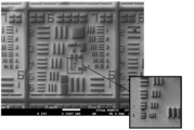
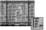
- 1 is an electron micrograph (magnification: 150 times) of a pattern formed by patterning the photocurable resin composition of Example 1 by photolithography.
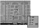
- 5 is an electron micrograph (magnification: 150 times) of a pattern formed by patterning the photocurable resin composition of Example 5 by photolithography.
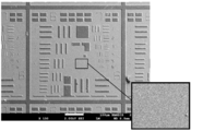
- 3 is an electron micrograph (magnification: 150 times) of a pattern formed by patterning the photocurable resin composition of Comparative Example 1 by photolithography.
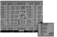
- 8 is an electron micrograph (magnification: 150 times) of a pattern formed by patterning the photocurable resin composition of Comparative Example 7 by photolithography.
- 9 is an electron micrograph (magnification: 150 times) of a pattern formed by patterning the photocurable resin composition of Comparative Example 8 by photolithography.
- the present invention includes the following components (A) to (D): (A) Modified polyphenylene ether resin (B) Bifunctional acrylic resin (C) Photopolymerization initiator (D) Coupling agent is included, and the mass ratio of the component (A) and the component (B) is 74.9:25. 1 to 49.9:50.1.
- the components (A) to (D) contained in the photocurable resin composition of the present invention will be described below.
- the photocurable resin composition of the present invention has the following formula (1): [In the formula, R 1 to R 3 each independently represent a hydrogen atom, an alkyl group, an alkenyl group or an alkynyl group, X represents a q-valent unsubstituted or substituted aromatic hydrocarbon group, Y is the following formula (2): [In the formula, R 4 to R 7 each independently represent a hydrogen atom, an alkyl group, an alkenyl group, an alkynyl group or an alkenylcarbonyl group.
- an x-valent (x represents an integer of 1 or more) hydrocarbon group refers to an x-valent group formed by removing x hydrogen atoms from a carbon atom of a hydrocarbon. Therefore, the above-mentioned q-valent unsubstituted or substituted aromatic hydrocarbon group means 1 to 4 produced by removing 1 to 4 hydrogen atoms from carbon atoms of an aromatic hydrocarbon which may be substituted or not. Refers to a tetravalent group.
- alkyl group means a monovalent saturated hydrocarbon group.
- the alkyl group is preferably a C 1 -C 10 alkyl group, more preferably a C 1 -C 6 alkyl group, still more preferably a C 1 -C 4 alkyl group, particularly preferably a C 1 -C 2 alkyl group.
- alkyl group include a methyl group, an ethyl group, a propyl group, an isopropyl group, a butyl group, an isobutyl group, a sec-butyl group, a tert-butyl group, a pentyl group and a hexyl group.
- alkenyl group means a monovalent unsaturated hydrocarbon group having at least one carbon-carbon double bond.
- the alkenyl group is preferably a C 2 -C 10 alkenyl group, more preferably a C 2 -C 6 alkenyl group, still more preferably a C 2 -C 4 alkenyl group.
- alkenyl group include ethenyl group (vinyl group), 1-propenyl group, 2-propenyl group, 1-butenyl group, 2-butenyl group, isobutenyl group, 1-pentenyl group, 1-hexenyl group and the like. be able to.
- the group —CR 1 ⁇ CR 2 R 3 in the above formula (1) is also an alkenyl group.
- alkynyl group means an unsaturated hydrocarbon group having at least one carbon-carbon triple bond.
- the alkynyl group is preferably C 2 -C 10 alkynyl group, more preferably C 2 -C 6 alkynyl group, still more preferably C 2 -C 4 alkynyl group.
- alkynyl group include ethynyl group, 1-propynyl group, 2-propynyl group, butynyl group, isobutynyl group, pentynyl group, hexynyl group and the like.
- alkenylcarbonyl group means a carbonyl group substituted with the above alkenyl group, and examples thereof include an acryloyl group and a methacryloyl group.
- the portion represented by -(Y) m- corresponds to the main chain of the PPE resin.
- R 4 and R 6 in the above-mentioned unsubstituted or substituted phenol repeating unit Y represent a hydrogen atom
- R 5 and R 7 represent a methyl group.
- the alkenyl group —CR 1 ⁇ CR 2 R 3 may be located at any of the ortho position, the meta position and the para position with respect to the methylene group.
- n in formula (1) is an integer from 1 to 4. In one aspect, n in formula (1) is 1 or 2. In one aspect, n in formula (1) is 1. In another embodiment, R 1 to R 3 in formula (1) are all hydrogen atoms.
- the number m of the repeating unit Y is preferably 1 to 80, more preferably 1 to 30, and further preferably 1 to 5.
- each of the aromatic hydrocarbon groups X is bonded with q moieties represented by —(Y) m — via an oxygen atom.
- q is 2 or 3. More preferably, q is 2.
- X is preferably the following formula: [Wherein, R 11 to R 18 each independently represent a hydrogen atom or a C 1 -C 6 alkyl group. ] It has a structure represented by.
- X is more preferably the following formula: It has a structure represented by.
- the number average molecular weight of the component (A) is preferably 500 or more and 5000 or less.
- the toughness of the cured product obtained by curing the photocurable resin composition of the present invention may be lowered.
- the compatibility of the component (A) with other components, especially with a solvent that is optionally added decreases.
- the number average molecular weight of the component (A) is more preferably 750 or more and 3000 or less, and further preferably 1000 or more and 2500 or less.
- the number average molecular weight of the component (A) can be measured by a known method, for example, gel permeation chromatography.
- the content of the component (A) in the photocurable resin composition of the present invention is not particularly limited, but is preferably 0.1 to 30 parts by mass relative to 100 parts by mass of the photocurable resin composition of the present invention. , More preferably 0.5 to 20 parts by mass, still more preferably 1 to 15 parts by mass.
- the component (A) can be obtained as a commercially available product (for example, OPE 2St 1200 (manufactured by Mitsubishi Gas Chemical Co., Inc.)).
- the component (A) can be prepared by a known method.
- a suitable q-valent phenol (2,2′,3,3′,5,5′) having a structure represented by X—(OH) q (wherein X and q have the same meanings as described above).
- -Hexamethylbiphenyl-4,4'-diol etc. and the following formula: [In the formula, each of R 4 to R 7 has the same meaning as described above.
- a suitable monohydric phenol having a structure represented by (2,6-dimethylphenol, etc.) is oxidatively copolymerized by a known method to prepare a polyphenylene ether resin having a hydroxyl group at the terminal and obtained.
- Component (A) can be prepared by methods involving modifying the resin by reaction with a suitable modifier, such as chloromethylstyrene.
- the component (A) can be prepared by the method described in JP-A-2008-260941 using a polyphenylene ether resin having a number average molecular weight (for example, more than 10,000) higher than that of the component (A) as a raw material. ..
- the photocurable resin composition of the present invention has the following formula (3): [In the formula, Each R a independently represents a hydrogen atom or a methyl group, Each R b independently represents a divalent hydrocarbon group, x and y each independently represent an integer of 1 to 5. ] It contains a bifunctional acrylic resin represented by. Hereinafter, this specific bifunctional acrylic resin may be referred to as “component (B)”.
- the component (B) used in the present invention reacts with the modified PPE resin (component (A)) by the action of a photopolymerization initiator to be described later and cures (hereinafter, this reaction may be referred to as "curing reaction”). is there). Further, by using the component (B), even if the low molecular weight component (A) is used for the purpose of enhancing the fluidity of the photocurable resin composition of the present invention, a cured product obtained by curing the same composition The heat resistance, etc. of is maintained.
- the resin used as the component (B) may be used alone or in combination of two or more kinds.
- the component (B) is bifunctional, that is, it has two acryloyloxy groups.
- a resin composition containing a monofunctional acrylic resin (acrylic resin having one acryloyloxy group) is sufficiently cured even if it is subjected to a curing treatment under conditions in which the photocurable resin composition of the present invention is sufficiently cured.
- a resin composition containing an acrylic resin having three or more acryloyloxy groups is also not sufficiently cured even when it is subjected to a curing treatment under conditions in which the photocurable resin composition of the present invention is sufficiently cured.
- such a resin composition has an insufficient affinity for the substrate.
- the photocurable resin composition of the present invention has excellent film forming properties, and provides a uniform thin film by a relatively simple film forming method such as spin coating. It is speculated that the bifunctionality of the component (B) is also involved in this excellent film-forming property.
- each R b in formula (3) is independently a methylene group or a p-phenylene group. In another aspect, R b in the formula (3) is a methylene group, and R a is a methyl group. In another aspect, R b in formula (3) is a p-phenylene group, and R a is a hydrogen atom.
- Examples of compounds that can be used as the component (B) include ethoxylated bisphenol A diacrylate (diacrylate of bisphenol A bound with (poly)ethylene glycol) and propoxylated bisphenol A diacrylate ((poly)propylene glycol).
- Examples include, but are not limited to, neopentyl glycol diacrylate). These may be used alone or in combination of two or more.
- the mass ratio of the component (A) to the component (B) is 74.9:25.1 to 49.9:50.1.
- the mass ratio of the component (A) and the component (B) is out of the above range, when the photocurable resin composition is cured on a substrate, the obtained cured product has poor adhesion to the substrate. It is enough.
- the mass ratio of the component (A) and the component (B) is particularly preferably 66.7:33.3 to 50.2:49.8.
- the content of the component (B) in the photocurable resin composition of the present invention is not particularly limited, but is preferably 20 to 50 parts by mass with respect to 100 parts by mass of the photocurable resin composition of the present invention.
- the amount is preferably 25 to 50 parts by mass, more preferably 30 to 47 parts by mass.
- the component (B) can be obtained as a commercially available product (for example, SR601 and SR9003B (manufactured by Arkema)).
- the component (B) can be prepared by a known method. For example, reacting a suitable diol compound having the structure represented by (CH 3 ) 2 C(R b OH) 2 where R b has the same meaning as above with ethylene oxide or propylene oxide
- Component (B) can be prepared by a method that involves reacting the resulting product with acrylic acid or a derivative thereof.
- the photocurable resin composition of the present invention contains a photopolymerization initiator.
- the photopolymerization initiator may be referred to as "component (C)".
- the component (C) used in the present invention is not particularly limited as long as it is a compound that generates a radical or the like that cures the above components (A) and (B) by irradiating with active energy rays.
- the active energy rays are in a broad sense such as radiation such as ⁇ rays and ⁇ rays, electromagnetic waves such as ⁇ rays and X rays, electron rays (EB), ultraviolet rays of about 100 to 400 nm, and visible rays of about 400 to 800 nm. It includes all light, and is preferably ultraviolet light.
- the compound used as the component (C) may be used alone or in combination of two or more kinds.
- component (C) examples include acetophenone photopolymerization initiator, benzoin photopolymerization initiator, benzophenone photopolymerization initiator, thioxanthone photopolymerization initiator, acylphosphine oxide photopolymerization initiator, oxime ester photopolymerization initiator.
- acetophenone photopolymerization initiator examples include acetophenone photopolymerization initiator, benzoin photopolymerization initiator, benzophenone photopolymerization initiator, thioxanthone photopolymerization initiator, acylphosphine oxide photopolymerization initiator, oxime ester photopolymerization initiator.
- acylphosphine oxide photopolymerization initiators and oxime ester photopolymerization initiators are preferable. These may be used alone or in combination of two or more.
- acylphosphine oxide photopolymerization initiator examples include bis(2,4,6-trimethylbenzoyl)-phenyl-phosphine oxide and 2,4,6-trimethylbenzoyl-diphenyl-phosphine oxide. It is not limited to these.
- oxime ester-based photopolymerization initiator examples include 1-[9-ethyl-6-(2-methylbenzoyl)-9H-carbazol-3-yl]-ethanone 1-(O-acetyloxime), 1- Examples include, but are not limited to, [4-(phenylthio)phenyl]-1,2-octanedione 2-(o-benzoyloxime).
- the compounding amount of the component (C) in the photocurable resin composition of the present invention is not particularly limited, but is preferably 0.1 to 30 parts by mass relative to 100 parts by mass of the photocurable resin composition of the present invention. , More preferably 0.25 to 10 parts by mass, particularly preferably 0.5 to 5 parts by mass. If the blending amount of the component (C) is too small, the curing of the photocurable resin composition of the present invention will be insufficient, and the adhesion of the composition to the substrate will be reduced. On the other hand, if the amount of component (C) is too large, the curing of the photocurable resin composition of the present invention proceeds excessively. For this reason, when a thin film obtained by depositing the same composition is subjected to patterning by photolithography, even the masked portion is hardened, making it difficult to reproduce a fine pattern.
- the component (C) can be obtained as a commercially available product (for example, IRGACURE TPO, IRGACURE 819, IRGACURE 819DW, IRGACURE OXE01, IRGACURE OXE02 (manufactured by BASF), etc.).
- the photocurable resin composition of the present invention contains a coupling agent.
- the coupling agent has two or more different functional groups in the molecule, one of which is a functional group that chemically bonds to an inorganic material, and the other of which is chemically bonded to an organic material. It is a functional group. It is important that the photocurable resin composition of the present invention contains a coupling agent in order for the composition to exhibit sufficient adhesion to other materials.
- the coupling agent may be referred to as “component (D)”.
- component (D) examples include, but are not limited to, silane coupling agents, aluminum coupling agents, titanium coupling agents, and the like.
- the compound used as the component (D) may be used alone or in combination of two or more kinds.
- the component (D) is preferably a silane coupling agent.
- the functional group of the silane coupling agent include vinyl group, epoxy group, styryl group, methacrylic group, acryl group, amino group, isocyanurate group, ureido group, mercapto group, sulfide group, isocyanate group and the like. it can.
- the blending amount of component (D) in the photocurable resin composition of the present invention is not particularly limited, but is preferably 0.1 to 30 parts by mass with respect to 100 parts by mass of the photocurable resin composition of the present invention. It is more preferably 0.5 to 10 parts by mass, and particularly preferably 0.8 to 3 parts by mass. If the compounding amount of the component (D) is too small, the photocurable resin composition of the present invention does not exhibit sufficient adhesion to the substrate. On the other hand, if the blending amount of the component (D) is too large, voids, creeping out, etc. may occur.
- the component (D) can be obtained as a commercial product (for example, KBM 503, KBM 1003 (manufactured by Shin-Etsu Silicone), Coatosil MP200 (manufactured by Momentive Performance Materials Japan), etc.).
- the photocurable composition of the present invention may contain optional components, for example, the following filming agent, in addition to the above components (A) to (D).
- a filming agent can be added to the photocurable composition of the present invention.
- a film containing the photocurable composition of the present invention can be obtained by molding the photocurable composition of the present invention into a film by a known method. Since such a film facilitates disposing the photocurable composition of the present invention at the position where the redistribution layer is formed, it contributes to improvement in workability in forming the redistribution layer.
- the film forming agent imparts flexibility to the photocurable composition of the present invention. Addition of a filming agent facilitates obtaining a film containing the photocurable composition of the present invention and handling of such a film.
- the film forming agent may be referred to as “component (E)”.
- component (E) examples include, but are not limited to, phenoxy resin and acrylic resin.
- the phenoxy resin is a polyhydroxy polyether synthesized by a direct reaction of a dihydric phenol compound and epichlorohydrin or an addition polymerization reaction of a diglycidyl ether of a dihydric phenol compound and a dihydric phenol compound.
- the acrylic resin refers to a homopolymer or copolymer of acrylic acid and/or methacrylic acid, or their derivatives (for example, ester and amide).
- the compounding amount of the component (E) in the photocurable resin composition of the present invention is not particularly limited.
- Component (E) is a commercially available product (for example, bisphenol A type phenoxy resin 4250 (manufactured by Mitsubishi Chemical), bisphenol A type phenoxy resin Fx316 (manufactured by Nippon Steel & Sumitomo Metal), bisphenol A type phenoxy resin YP50 (manufactured by Nippon Steel & Sumitomo Metal), polymethyl methacrylate. -Butylacrylamide-triblock copolymer M52N (manufactured by Arkema, etc.)).
- the photocurable resin composition of the present invention is an optional component other than the component (E), for example, a stabilizer, a filler, a pigment, a plasticizer, a flame retardant, an ion trap agent, as long as the effects of the present invention are not impaired.
- a stabilizer for example, a stabilizer, a filler, a pigment, a plasticizer, a flame retardant, an ion trap agent, as long as the effects of the present invention are not impaired.
- An antifoaming agent, a leveling agent, a defoaming agent, a solvent and the like may be further contained.
- the photocurable resin composition of the present invention can be prepared by mixing the above components.
- a known device can be used for mixing.
- it can be mixed by a known device such as a Henschel mixer or a roll mill.
- These components may be mixed at the same time, or some of them may be mixed first and the rest of them may be mixed later.
- the photocurable resin composition of the present invention obtained as described above has the above-mentioned active energy rays, preferably light having a wavelength of 10 nm to 600 nm, more preferably ultraviolet light having a wavelength of 100 nm to 500 nm, and further preferably 250 nm to 450 nm. It can be easily cured by irradiation with ultraviolet rays, particularly preferably ultraviolet rays having a wavelength of 300 nm to 400 nm.
- the curing temperature is generally 0°C to 100°C, preferably 10°C to 50°C, more preferably 15°C to 35°C.
- the irradiation time may vary depending on the curing temperature and the volume of the resin composition to be cured, etc., but is usually 5 seconds to 60 minutes.
- the cured product thus obtained is excellent in electrical properties (particularly dielectric properties), heat resistance, adhesion to other materials, etc., and therefore the photocurable resin composition of the present invention constitutes a semiconductor device. It can be preferably used as a material for manufacturing an electronic component, such as an interlayer insulating film or a substrate.
- the photocurable resin composition of the present invention has an excellent film forming property, and gives a uniform thin film by a relatively simple film forming method such as spin coating.
- a thin film obtained by forming the photocurable resin composition of the present invention into a film is subjected to patterning by photolithography, a fine pattern can be reproduced well.
- the photocurable resin composition of the present invention can be sufficiently cured by irradiation with active energy rays (especially ultraviolet rays), and it is not necessary to treat the thin film after patterning at a high temperature (for example, 200° C. or higher). Therefore, there is no problem that the wiring pattern formed by patterning is deformed due to the shrinkage or the like generated during the high temperature treatment.
- the cured product obtained by curing the photocurable resin composition of the present invention is excellent not only in dielectric properties but also in heat resistance, and the cured product after patterning by photolithography is subjected to a treatment at a high temperature of about 200° C. However, if the processing time is up to about 1 hour, the formed pattern will not be deformed by heat. Due to such characteristics, the photocurable resin composition of the present invention is suitable as a material for electronic parts constituting a semiconductor device, particularly as a material for forming a rewiring layer in a wiring structure of electronic parts.
- the present invention also provides a cured product obtained by curing the photocurable resin composition of the present invention or a film containing the same.
- the present invention also provides a wiring structure including the cured product of the present invention, an electronic component including the cured product of the present invention, and a semiconductor device including the electronic component of the present invention.
- (A)) The compounds used as the component (A) in Examples and Comparative Examples are as follows.
- the compounds used as the component (B) in Examples and Comparative Examples are as follows.
- the compounds used as the component (B′) in the examples and comparative examples are as follows.
- the compounds used as the component (C) in the examples and comparative examples are as follows.
- C-1) IRGACURE OXE02 (oxime ester photopolymerization initiator (manufactured by BASF))
- C-2) IRGACURE 819 (acylphosphine oxide photopolymerization initiator (manufactured by BASF))
- component (D) Coupling agent
- D-1) KBM 503 (3-methacryloxypropyltrimethoxysilane (manufactured by Shin-Etsu Silicone))
- D-2) KBM 1003 (vinyltrimethoxysilane (manufactured by Shin-Etsu Silicone))
- D-3) Coatosil MP200 (epoxy group-modified silane coupling agent (manufactured by Momentive Performance Materials Japan))
- a photocurable resin composition was prepared by mixing each component in a predetermined amount using a rotation/revolution mixer (ARE-310 manufactured by THINKY).
- the resulting photocurable resin composition was spin-coated using a spin coater (WS-650-8B (manufactured by Laurell)) (conditions: 500 rpm for 12 seconds, then 1500 rpm for 20 seconds (acceleration 1200)) to a diameter of 150 mm.
- WS-650-8B manufactured by Laurell
- This silicon wafer was heated at 120° C. for 5 minutes in an air atmosphere and dried to obtain a sample composed of a silicon wafer and a uniform thin film having a thickness of 4.81 ⁇ m formed thereon. This sample was subjected to the following photolithography test, and the suitability of the photocurable resin composition for photolithography was evaluated. The results are shown in Table 1.
- a mask (thickness: 1.5 mm, USAF pattern manufactured by Advance Reproductions) was placed on the thin film surface of the above sample, and the sample was subjected to ultraviolet irradiation under the following conditions while the mask was in close contact with the thin film surface.
- the mask has a large number of rectangular (450 ⁇ m ⁇ 450 ⁇ m) regions, and the same wiring pattern is drawn in these regions.
- UV irradiation conditions Ultraviolet irradiation device Bluewave (registered trademark) QX4 (manufactured by DYMAX) (A LED head RediCure (trademark) (manufactured by DYMAX) is attached as a light source) UV wavelength: 365nm Irradiation intensity: Approx. 200 mW/cm Irradiation time: 10 seconds Mask-light source distance: 50 mm
- the mask was removed from the sample, the sample was washed three times with cyclopentanone, and then heated at 200° C. for 1 hour in the air atmosphere and dried. After the completion of drying, the surface of the thin film in the sample was observed with a scanning electron microscope (magnification: 150 times) to examine whether or not the wiring pattern was clearly reproduced on the thin film.
- Curing of the photocurable resin composition of the present invention can be sufficiently achieved by irradiation with ordinary active energy rays (for example, ultraviolet rays) and does not require high temperature treatment. Therefore, problems such as deformation due to high temperature treatment do not occur.
- the cured product thus obtained is excellent in electrical properties (particularly dielectric properties), heat resistance, and adhesion to other materials. Therefore, the photocurable resin composition of the present invention can be suitably used as a material for manufacturing an electronic component that constitutes a semiconductor device, particularly as a material for forming a rewiring layer.
Landscapes
- Chemical & Material Sciences (AREA)
- Organic Chemistry (AREA)
- Chemical Kinetics & Catalysis (AREA)
- Health & Medical Sciences (AREA)
- Medicinal Chemistry (AREA)
- Polymers & Plastics (AREA)
- Physics & Mathematics (AREA)
- Spectroscopy & Molecular Physics (AREA)
- General Physics & Mathematics (AREA)
- Materials Engineering (AREA)
- Life Sciences & Earth Sciences (AREA)
- Engineering & Computer Science (AREA)
- Wood Science & Technology (AREA)
- Inorganic Chemistry (AREA)
- Macromonomer-Based Addition Polymer (AREA)
- Materials For Photolithography (AREA)
- Polymerization Catalysts (AREA)
Priority Applications (5)
| Application Number | Priority Date | Filing Date | Title |
|---|---|---|---|
| CN202080013860.2A CN113423750B (zh) | 2019-02-12 | 2020-01-22 | 光固化性树脂组合物和使其固化而得到的固化物 |
| JP2020572139A JP7401917B2 (ja) | 2019-02-12 | 2020-01-22 | 光硬化性樹脂組成物及びそれを硬化させて得られる硬化物 |
| US17/429,988 US20220144993A1 (en) | 2019-02-12 | 2020-01-22 | Photocurable resin composition and cured product obtained by curing the same |
| EP20755435.3A EP3925993B1 (en) | 2019-02-12 | 2020-01-22 | Photocurable resin composition and cured product obtained by curing same |
| KR1020217028816A KR102801857B1 (ko) | 2019-02-12 | 2020-01-22 | 광 경화성 수지 조성물 및 그것을 경화시켜 얻어지는 경화물 |
Applications Claiming Priority (2)
| Application Number | Priority Date | Filing Date | Title |
|---|---|---|---|
| US201962804337P | 2019-02-12 | 2019-02-12 | |
| US62/804,337 | 2019-02-12 |
Publications (1)
| Publication Number | Publication Date |
|---|---|
| WO2020166288A1 true WO2020166288A1 (ja) | 2020-08-20 |
Family
ID=72044068
Family Applications (1)
| Application Number | Title | Priority Date | Filing Date |
|---|---|---|---|
| PCT/JP2020/002100 Ceased WO2020166288A1 (ja) | 2019-02-12 | 2020-01-22 | 光硬化性樹脂組成物及びそれを硬化させて得られる硬化物 |
Country Status (7)
| Country | Link |
|---|---|
| US (1) | US20220144993A1 (enExample) |
| EP (1) | EP3925993B1 (enExample) |
| JP (1) | JP7401917B2 (enExample) |
| KR (1) | KR102801857B1 (enExample) |
| CN (1) | CN113423750B (enExample) |
| TW (1) | TWI813852B (enExample) |
| WO (1) | WO2020166288A1 (enExample) |
Cited By (3)
| Publication number | Priority date | Publication date | Assignee | Title |
|---|---|---|---|---|
| WO2022004285A1 (ja) * | 2020-07-01 | 2022-01-06 | ナミックス株式会社 | 感光性樹脂組成物、その硬化物、及びその硬化物を含む配線構造体 |
| JP2023130779A (ja) * | 2022-03-08 | 2023-09-21 | 日本化薬株式会社 | 硬化性樹脂組成物、その硬化物および半導体装置 |
| WO2025074949A1 (ja) * | 2023-10-04 | 2025-04-10 | ダウ・東レ株式会社 | 紫外線硬化性組成物 |
Citations (11)
| Publication number | Priority date | Publication date | Assignee | Title |
|---|---|---|---|---|
| JP2003515642A (ja) * | 1999-12-01 | 2003-05-07 | ゼネラル・エレクトリック・カンパニイ | ポリ(フェニレンエーテル)−ポリビニル熱硬化性樹脂 |
| JP2004294882A (ja) | 2003-03-27 | 2004-10-21 | Nippon Steel Chem Co Ltd | 感光性樹脂組成物及び硬化物 |
| WO2005073264A1 (ja) * | 2004-01-30 | 2005-08-11 | Nippon Steel Chemical Co., Ltd. | 硬化性樹脂組成物 |
| JP2006513301A (ja) * | 2003-01-14 | 2006-04-20 | ゼネラル・エレクトリック・カンパニイ | ポリ(フェニレンエーテル)−ポリビニル熱硬化性接着剤、フィルム、及びそれから製造した基板 |
| JP2007112826A (ja) * | 2005-10-18 | 2007-05-10 | Matsushita Electric Works Ltd | 樹脂組成物、プリプレグ、積層体 |
| JP2008260941A (ja) | 2003-01-28 | 2008-10-30 | Matsushita Electric Works Ltd | ポリフェニレンエーテル樹脂組成物、プリプレグ、積層板 |
| JP2009186861A (ja) | 2008-02-08 | 2009-08-20 | Asahi Kasei E-Materials Corp | 感光性樹脂組成物 |
| JP2017047648A (ja) * | 2015-09-04 | 2017-03-09 | 三菱瓦斯化学株式会社 | 銅張積層板 |
| WO2017135168A1 (ja) * | 2016-02-02 | 2017-08-10 | 三菱瓦斯化学株式会社 | 樹脂組成物、プリプレグ、金属箔張積層板、樹脂シート、プリント配線板及び半導体装置 |
| JP2018028078A (ja) * | 2016-08-10 | 2018-02-22 | パナソニックIpマネジメント株式会社 | 封止用アクリル組成物、シート材、積層シート、硬化物、半導体装置及び半導体装置の製造方法 |
| WO2019130735A1 (ja) * | 2017-12-28 | 2019-07-04 | パナソニックIpマネジメント株式会社 | ポリフェニレンエーテル樹脂組成物、並びに、それを用いたプリプレグ、樹脂付きフィルム、樹脂付き金属箔、金属張積層板及び配線基板 |
Family Cites Families (9)
| Publication number | Priority date | Publication date | Assignee | Title |
|---|---|---|---|---|
| CN100387103C (zh) * | 1999-08-12 | 2008-05-07 | Ibiden股份有限公司 | 多层印刷电路板和半导体器件 |
| CN1756655A (zh) * | 2003-01-14 | 2006-04-05 | 通用电气公司 | 聚(亚苯基醚)-聚乙烯基热固性粘合剂膜和由其制造的基体 |
| US7329708B2 (en) * | 2004-08-18 | 2008-02-12 | General Electric Company | Functionalized poly(arylene ether) composition and method |
| JP5439075B2 (ja) * | 2009-07-21 | 2014-03-12 | 太陽ホールディングス株式会社 | 光硬化性樹脂組成物 |
| US10030133B2 (en) * | 2011-12-06 | 2018-07-24 | Kaneka Corporation | Black photosensitive resin composition and use of same |
| CN107108782B (zh) * | 2014-12-26 | 2019-12-03 | 日铁化学材料株式会社 | 末端改性可溶性多官能乙烯基芳香族共聚合物及其应用 |
| JP6550275B2 (ja) * | 2015-06-15 | 2019-07-24 | 東京応化工業株式会社 | ナノインプリント用組成物、硬化物、パターン形成方法及びパターンを含む物品 |
| TWI686436B (zh) * | 2018-08-28 | 2020-03-01 | 台燿科技股份有限公司 | 無鹵素低介電樹脂組合物,以及使用該組合物所製得之預浸漬片、金屬箔積層板與印刷電路板 |
| CN112646350B (zh) * | 2019-10-11 | 2023-04-25 | 台光电子材料(昆山)有限公司 | 一种树脂组合物及其制品 |
-
2020
- 2020-01-22 JP JP2020572139A patent/JP7401917B2/ja active Active
- 2020-01-22 EP EP20755435.3A patent/EP3925993B1/en active Active
- 2020-01-22 CN CN202080013860.2A patent/CN113423750B/zh active Active
- 2020-01-22 WO PCT/JP2020/002100 patent/WO2020166288A1/ja not_active Ceased
- 2020-01-22 KR KR1020217028816A patent/KR102801857B1/ko active Active
- 2020-01-22 TW TW109102578A patent/TWI813852B/zh active
- 2020-01-22 US US17/429,988 patent/US20220144993A1/en not_active Abandoned
Patent Citations (11)
| Publication number | Priority date | Publication date | Assignee | Title |
|---|---|---|---|---|
| JP2003515642A (ja) * | 1999-12-01 | 2003-05-07 | ゼネラル・エレクトリック・カンパニイ | ポリ(フェニレンエーテル)−ポリビニル熱硬化性樹脂 |
| JP2006513301A (ja) * | 2003-01-14 | 2006-04-20 | ゼネラル・エレクトリック・カンパニイ | ポリ(フェニレンエーテル)−ポリビニル熱硬化性接着剤、フィルム、及びそれから製造した基板 |
| JP2008260941A (ja) | 2003-01-28 | 2008-10-30 | Matsushita Electric Works Ltd | ポリフェニレンエーテル樹脂組成物、プリプレグ、積層板 |
| JP2004294882A (ja) | 2003-03-27 | 2004-10-21 | Nippon Steel Chem Co Ltd | 感光性樹脂組成物及び硬化物 |
| WO2005073264A1 (ja) * | 2004-01-30 | 2005-08-11 | Nippon Steel Chemical Co., Ltd. | 硬化性樹脂組成物 |
| JP2007112826A (ja) * | 2005-10-18 | 2007-05-10 | Matsushita Electric Works Ltd | 樹脂組成物、プリプレグ、積層体 |
| JP2009186861A (ja) | 2008-02-08 | 2009-08-20 | Asahi Kasei E-Materials Corp | 感光性樹脂組成物 |
| JP2017047648A (ja) * | 2015-09-04 | 2017-03-09 | 三菱瓦斯化学株式会社 | 銅張積層板 |
| WO2017135168A1 (ja) * | 2016-02-02 | 2017-08-10 | 三菱瓦斯化学株式会社 | 樹脂組成物、プリプレグ、金属箔張積層板、樹脂シート、プリント配線板及び半導体装置 |
| JP2018028078A (ja) * | 2016-08-10 | 2018-02-22 | パナソニックIpマネジメント株式会社 | 封止用アクリル組成物、シート材、積層シート、硬化物、半導体装置及び半導体装置の製造方法 |
| WO2019130735A1 (ja) * | 2017-12-28 | 2019-07-04 | パナソニックIpマネジメント株式会社 | ポリフェニレンエーテル樹脂組成物、並びに、それを用いたプリプレグ、樹脂付きフィルム、樹脂付き金属箔、金属張積層板及び配線基板 |
Cited By (4)
| Publication number | Priority date | Publication date | Assignee | Title |
|---|---|---|---|---|
| WO2022004285A1 (ja) * | 2020-07-01 | 2022-01-06 | ナミックス株式会社 | 感光性樹脂組成物、その硬化物、及びその硬化物を含む配線構造体 |
| JP2023130779A (ja) * | 2022-03-08 | 2023-09-21 | 日本化薬株式会社 | 硬化性樹脂組成物、その硬化物および半導体装置 |
| JP7744268B2 (ja) | 2022-03-08 | 2025-09-25 | 日本化薬株式会社 | 硬化性樹脂組成物、その硬化物および半導体装置 |
| WO2025074949A1 (ja) * | 2023-10-04 | 2025-04-10 | ダウ・東レ株式会社 | 紫外線硬化性組成物 |
Also Published As
| Publication number | Publication date |
|---|---|
| US20220144993A1 (en) | 2022-05-12 |
| EP3925993A4 (en) | 2022-11-09 |
| KR20210127959A (ko) | 2021-10-25 |
| CN113423750A (zh) | 2021-09-21 |
| TW202035597A (zh) | 2020-10-01 |
| EP3925993A1 (en) | 2021-12-22 |
| CN113423750B (zh) | 2023-11-21 |
| KR102801857B1 (ko) | 2025-05-02 |
| EP3925993B1 (en) | 2023-09-13 |
| JPWO2020166288A1 (ja) | 2021-12-16 |
| JP7401917B2 (ja) | 2023-12-20 |
| TWI813852B (zh) | 2023-09-01 |
Similar Documents
| Publication | Publication Date | Title |
|---|---|---|
| TWI687479B (zh) | 感光性樹脂組成物 | |
| TWI529489B (zh) | 光固化性及熱固性樹脂組成物、其製造之防焊乾膜及包含該防焊乾膜之電路板 | |
| JP7401917B2 (ja) | 光硬化性樹脂組成物及びそれを硬化させて得られる硬化物 | |
| TW201809028A (zh) | 硬化性樹脂組成物、乾膜、硬化物及印刷配線板 | |
| TW201142499A (en) | Photo-curable and thermo-curable resin composition, and dry film solder resist | |
| JP7240009B2 (ja) | 感光性樹脂組成物、ドライフィルム、及びプリント配線板 | |
| KR100677782B1 (ko) | 절연막 형성용 재료의 제조 방법 | |
| JP7069081B2 (ja) | シリカゾルを含んだ感光性樹脂組成物、及びこれを用いた硬化物 | |
| CN110955115A (zh) | 树脂组合物、感光性膜、带支承体的感光性膜、印刷布线板和半导体装置 | |
| CN117908328A (zh) | 感光性树脂组合物、干膜、固化物和印刷布线板 | |
| WO2022259933A1 (ja) | 感光性樹脂組成物、樹脂膜、電子装置および電子装置の製造方法 | |
| JP7619654B2 (ja) | 感光性樹脂組成物、その硬化物、及びその硬化物を含む配線構造体 | |
| KR20180029853A (ko) | 상분리 구조 형성용 수지 조성물, 및 상분리 구조를 포함하는 구조체의 제조 방법 | |
| CN109254498B (zh) | 感光性树脂组合物 | |
| JP7229304B2 (ja) | 感光性樹脂組成物及び感光性樹脂組成物を塗布したプリント配線板 | |
| TWI864686B (zh) | (甲基)丙烯酸酯系樹脂、樹脂組成物及乾膜阻焊劑 | |
| KR20230132089A (ko) | 감광성 수지 조성물 | |
| WO2023058425A1 (ja) | 樹脂組成物、半導体装置及び半導体装置の製造方法 | |
| WO2025142647A1 (ja) | 感光性樹脂組成物、硬化物および半導体装置 | |
| WO2025142645A1 (ja) | 感光性樹脂組成物、硬化物および半導体装置 | |
| TW202433175A (zh) | 阻焊劑用樹脂組合物 | |
| WO2024190410A1 (ja) | 半導体装置及び樹脂組成物 | |
| TW202439023A (zh) | 感光性樹脂組成物、感光性元件、印刷配線板及印刷配線板之製造方法 | |
| TW202314383A (zh) | 光敏感樹脂組成物 | |
| WO2022118620A1 (ja) | 感光性ポリイミド樹脂組成物、樹脂膜及び電子装置 |
Legal Events
| Date | Code | Title | Description |
|---|---|---|---|
| 121 | Ep: the epo has been informed by wipo that ep was designated in this application |
Ref document number: 20755435 Country of ref document: EP Kind code of ref document: A1 |
|
| ENP | Entry into the national phase |
Ref document number: 2020572139 Country of ref document: JP Kind code of ref document: A |
|
| NENP | Non-entry into the national phase |
Ref country code: DE |
|
| ENP | Entry into the national phase |
Ref document number: 20217028816 Country of ref document: KR Kind code of ref document: A |
|
| ENP | Entry into the national phase |
Ref document number: 2020755435 Country of ref document: EP Effective date: 20210913 |