WO2020100949A1 - 弾性波装置、分波器および通信装置 - Google Patents
弾性波装置、分波器および通信装置 Download PDFInfo
- Publication number
- WO2020100949A1 WO2020100949A1 PCT/JP2019/044567 JP2019044567W WO2020100949A1 WO 2020100949 A1 WO2020100949 A1 WO 2020100949A1 JP 2019044567 W JP2019044567 W JP 2019044567W WO 2020100949 A1 WO2020100949 A1 WO 2020100949A1
- Authority
- WO
- WIPO (PCT)
- Prior art keywords
- electrode
- bus bar
- piezoelectric layer
- wave device
- elastic wave
- Prior art date
- Legal status (The legal status is an assumption and is not a legal conclusion. Google has not performed a legal analysis and makes no representation as to the accuracy of the status listed.)
- Ceased
Links
Images







Classifications
-
- H—ELECTRICITY
- H03—ELECTRONIC CIRCUITRY
- H03H—IMPEDANCE NETWORKS, e.g. RESONANT CIRCUITS; RESONATORS
- H03H9/00—Networks comprising electromechanical or electro-acoustic elements; Electromechanical resonators
- H03H9/02—Details
- H03H9/02535—Details of surface acoustic wave devices
- H03H9/02543—Characteristics of substrate, e.g. cutting angles
- H03H9/02574—Characteristics of substrate, e.g. cutting angles of combined substrates, multilayered substrates, piezoelectrical layers on not-piezoelectrical substrate
-
- H—ELECTRICITY
- H03—ELECTRONIC CIRCUITRY
- H03H—IMPEDANCE NETWORKS, e.g. RESONANT CIRCUITS; RESONATORS
- H03H9/00—Networks comprising electromechanical or electro-acoustic elements; Electromechanical resonators
- H03H9/02—Details
- H03H9/02228—Guided bulk acoustic wave devices or Lamb wave devices having interdigital transducers situated in parallel planes on either side of a piezoelectric layer
-
- H—ELECTRICITY
- H03—ELECTRONIC CIRCUITRY
- H03H—IMPEDANCE NETWORKS, e.g. RESONANT CIRCUITS; RESONATORS
- H03H9/00—Networks comprising electromechanical or electro-acoustic elements; Electromechanical resonators
- H03H9/02—Details
- H03H9/02007—Details of bulk acoustic wave devices
- H03H9/02062—Details relating to the vibration mode
-
- H—ELECTRICITY
- H03—ELECTRONIC CIRCUITRY
- H03H—IMPEDANCE NETWORKS, e.g. RESONANT CIRCUITS; RESONATORS
- H03H9/00—Networks comprising electromechanical or electro-acoustic elements; Electromechanical resonators
- H03H9/02—Details
- H03H9/02007—Details of bulk acoustic wave devices
- H03H9/02157—Dimensional parameters, e.g. ratio between two dimension parameters, length, width or thickness
-
- H—ELECTRICITY
- H03—ELECTRONIC CIRCUITRY
- H03H—IMPEDANCE NETWORKS, e.g. RESONANT CIRCUITS; RESONATORS
- H03H9/00—Networks comprising electromechanical or electro-acoustic elements; Electromechanical resonators
- H03H9/02—Details
- H03H9/125—Driving means, e.g. electrodes, coils
- H03H9/13—Driving means, e.g. electrodes, coils for networks consisting of piezoelectric or electrostrictive materials
- H03H9/132—Driving means, e.g. electrodes, coils for networks consisting of piezoelectric or electrostrictive materials characterized by a particular shape
-
- H—ELECTRICITY
- H03—ELECTRONIC CIRCUITRY
- H03H—IMPEDANCE NETWORKS, e.g. RESONANT CIRCUITS; RESONATORS
- H03H9/00—Networks comprising electromechanical or electro-acoustic elements; Electromechanical resonators
- H03H9/02—Details
- H03H9/125—Driving means, e.g. electrodes, coils
- H03H9/145—Driving means, e.g. electrodes, coils for networks using surface acoustic waves
- H03H9/14544—Transducers of particular shape or position
- H03H9/1457—Transducers having different finger widths
-
- H—ELECTRICITY
- H03—ELECTRONIC CIRCUITRY
- H03H—IMPEDANCE NETWORKS, e.g. RESONANT CIRCUITS; RESONATORS
- H03H9/00—Networks comprising electromechanical or electro-acoustic elements; Electromechanical resonators
- H03H9/15—Constructional features of resonators consisting of piezoelectric or electrostrictive material
- H03H9/17—Constructional features of resonators consisting of piezoelectric or electrostrictive material having a single resonator
- H03H9/171—Constructional features of resonators consisting of piezoelectric or electrostrictive material having a single resonator implemented with thin-film techniques, i.e. of the film bulk acoustic resonator [FBAR] type
- H03H9/172—Means for mounting on a substrate, i.e. means constituting the material interface confining the waves to a volume
- H03H9/175—Acoustic mirrors
-
- H—ELECTRICITY
- H03—ELECTRONIC CIRCUITRY
- H03H—IMPEDANCE NETWORKS, e.g. RESONANT CIRCUITS; RESONATORS
- H03H9/00—Networks comprising electromechanical or electro-acoustic elements; Electromechanical resonators
- H03H9/25—Constructional features of resonators using surface acoustic waves
Definitions
- the present disclosure relates to an elastic wave device that uses an elastic wave, a duplexer including the elastic wave device, and a communication device.
- An elastic wave device that applies a voltage to an IDT (interdigital transducer) electrode on a piezoelectric body to generate an elastic wave propagating through the piezoelectric body.
- the IDT electrode has a pair of comb-teeth electrodes.
- Each of the pair of comb-teeth electrodes has a plurality of electrode fingers and is arranged so as to mesh with each other.
- a standing wave of an elastic wave having a wavelength that is twice the pitch of the electrode fingers is formed, and the frequency of this standing wave becomes the resonance frequency.
- an elastic wave device using a plate wave among elastic waves has been proposed.
- a substrate, an acoustic reflection layer located on the substrate, a piezoelectric layer located on the acoustic reflection layer, and an IDT electrode located on the piezoelectric layer are provided.
- the acoustic reflection layer is configured by alternately stacking low acoustic impedance layers and high acoustic impedance layers. With such a configuration, it is possible to provide an acoustic wave device having a resonance point at 5 GHz even when the electrode finger period is about 3 ⁇ m.
- An elastic wave device includes a piezoelectric layer and an IDT electrode located on the piezoelectric layer.
- the IDT electrodes are connected to different potentials, and are connected to the first busbars and the second busbars spaced apart from each other and to the first busbars alternately arranged along the elastic wave propagation direction.
- a first electrode finger extending to the second bus bar side and a second electrode finger connected to the second bus bar and extending to the first bus bar side.
- the first electrode finger extends from a portion connected to the first bus bar to a position overlapping the tip of the second electrode finger when viewed in the arrangement direction of the first electrode finger and the second electrode finger.
- the widened portion has a thickness that is thicker than the vicinity of the center of the intersecting region of the first electrode finger and the second electrode finger.
- the thickness of the piezoelectric layer is less than 1.5p, where p is the pitch of the electrode fingers of the IDT electrodes.
- An elastic wave device uses an A1 mode plate wave having a piezoelectric layer and an IDT electrode located on the piezoelectric layer.
- the IDT electrodes are connected to different potentials, and are connected to the first busbars and the second busbars spaced apart from each other and to the first busbars alternately arranged along the elastic wave propagation direction.
- a first electrode finger extending to the second bus bar side and a second electrode finger connected to the second bus bar and extending to the first bus bar side.
- the first electrode finger extends from a portion connected to the first bus bar to a position overlapping the tip of the second electrode finger when viewed in the arrangement direction of the first electrode finger and the second electrode finger.
- the widened portion has a thickness that is thicker than the vicinity of the center of the intersecting region of the first electrode finger and the second electrode finger.
- a duplexer includes an antenna terminal, a transmission filter that filters a signal output to the antenna terminal, and a reception filter that filters a signal input from the antenna terminal. At least one of the transmission filter and the reception filter includes the acoustic wave device.
- a communication device includes an antenna, the above-described duplexer in which the antenna terminal is connected to the antenna, and the antenna terminal with respect to a signal path with respect to the transmission filter and the reception filter. And an IC connected to the opposite side.
- FIG. 1 is a plan view of an elastic wave device according to an embodiment.
- FIG. 2 is a sectional view taken along the line II-II of the elastic wave device of FIG. 1. It is a principal part enlarged view of FIG.
- FIG. 4 is a diagram showing electrode finger models of Examples and Comparative Examples.
- 5A is a diagram showing impedance characteristics of the example and the comparative example
- FIG. 5B is a diagram showing phase characteristics of the example and the comparative example.
- FIG. 5D is an enlarged view of a main part of FIG.
- FIG. 6A is a diagram showing the correlation between the offset amount and the resonance frequency
- FIG. 6B is a diagram showing the correlation between the offset amount and df and the maximum phase.
- FIG. 6A is a diagram showing the correlation between the offset amount and the resonance frequency
- FIG. 6B is a diagram showing the correlation between the offset amount and df and the maximum phase.
- FIG. 7A is a diagram showing impedance characteristics of the example and the comparative example
- FIG. 7B is a diagram showing phase characteristics of the example and the comparative example
- FIG. 7D is an enlarged view of a main part of FIG.
- FIG. 8A is a diagram showing the correlation between the offset amount and the resonance frequency
- FIG. 8B is a diagram showing the correlation between the offset amount and df and the maximum phase.
- It is a circuit diagram which shows typically the structure of the demultiplexer as an example of utilization of the elastic wave apparatus of FIG.
- It is a circuit diagram which shows typically the structure of the communication apparatus as an example of utilization of the elastic wave apparatus of FIG. 11A and 11B are diagrams showing the correlation between the offset amount and the maximum phase value.
- FIG. 11A and 11B are diagrams showing the correlation between the offset amount and the maximum phase value.
- FIG. 12A is a diagram showing the relationship between the duty at the widened portion and the frequency characteristic
- FIG. 12B is a diagram showing the relationship between the duty at the widened portion and the duty at the intersection.
- 13A is a diagram showing the relationship between the duty at the widened portion and the frequency characteristic
- FIG. 13B is a diagram showing the relationship between the duty at the widened portion and the duty at the intersecting portion.
- FIG. 15B is a diagram showing phase characteristics of the example and the comparative example.
- FIG. 15D is an enlarged view of a main part of FIG. FIG.
- FIG. 16 is a diagram showing electrode finger models of Examples and Comparative Examples.
- 17A is a diagram showing impedance characteristics of the example and the comparative example
- FIG. 17B is a diagram showing phase characteristics of the example and the comparative example
- FIGS. 17D is an enlarged view of a main part of FIG. 17B.
- the acoustic wave device may be either up or down, but for convenience, an orthogonal coordinate system including D1, D2, and D3 axes will be defined below.
- the positive side of the D3 axis is the upper side, and terms such as the upper surface or the lower surface are sometimes used.
- the term “planar view” or “planar see-through” means looking in the D3 axis direction unless otherwise specified.
- the D1 axis is defined to be parallel to the propagation direction of elastic waves propagating along the upper surface of the piezoelectric layer described later
- the D2 axis is defined to be parallel to the upper surface of the piezoelectric layer and orthogonal to the D1 axis.
- the D3 axis is defined to be orthogonal to the upper surface of the piezoelectric layer.
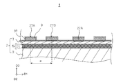
- FIG. 1 is a plan view showing a configuration of a main part of the acoustic wave device 1.
- FIG. 1 shows a structure of a resonator described later.
- FIG. 2 is a sectional view taken along line II-II in FIG.
- the acoustic wave device 1 is, for example, a substrate 3 (FIG. 2), a multilayer film 5 (FIG. 2) located on the substrate 3, a piezoelectric layer 7 located on the multilayer film 5, and a piezoelectric layer 7 located on the piezoelectric layer 7. And a conductive layer 9.
- Each layer has, for example, a substantially constant thickness.
- the combination of the substrate 3, the multilayer film 5 and the piezoelectric layer 7 may be referred to as the fixed substrate 2 (FIG. 2).
- the acoustic wave device 1 when a voltage is applied to the conductive layer 9, the acoustic wave propagating in the piezoelectric layer 7 is excited.
- the elastic wave device 1 constitutes, for example, a resonator and / or a filter that uses this elastic wave.
- the multilayer film 5 contributes to, for example, reflecting elastic waves and confining the energy of the elastic waves in the piezoelectric layer 7.
- the substrate 3 contributes to reinforcing the strength of the multilayer film 5 and the piezoelectric layer 7, for example.
- the acoustic wave device 1 may be the resonator shown in FIG. 1 alone, or may be provided with a plurality of resonators to form a filter or the like.
- the substrate 3 does not directly affect the electrical characteristics of the acoustic wave device 1. Therefore, the material and dimensions of the substrate 3 may be set appropriately.
- the material of the substrate 3 is, for example, an insulating material, and the insulating material is, for example, resin or ceramic.
- the substrate 3 may be made of a material having a coefficient of thermal expansion lower than that of the piezoelectric layer 7 and the like. In this case, for example, it is possible to reduce the risk that the frequency characteristics of the acoustic wave device 1 change due to temperature changes. Examples of such materials include semiconductors such as silicon, single crystals such as sapphire, and ceramics such as aluminum oxide sintered bodies.
- the substrate 3 may be configured by laminating a plurality of layers made of different materials. The substrate 3 is thicker than the piezoelectric layer 7, for example.
- the multilayer film 5 is configured by alternately stacking the low acoustic impedance layers 11 and the high acoustic impedance layers 13. As a result, the elastic wave reflectance becomes relatively high at the interface between the two. As a result, for example, leakage of elastic waves propagating through the piezoelectric layer 7 in the thickness direction is reduced.
- silicon dioxide SiO 2
- SiO 2 silicon dioxide
- Examples of the material forming the high acoustic impedance layer 13 include tantalum pentoxide (Ta 2 O 5 ), hafnium oxide (HfO 2 ), zirconium oxide (ZrO 2 ), and titanium oxide (TiO 2 ).
- the number of laminated layers of the multilayer film 5 may be set appropriately.
- the total number of laminated layers of the low acoustic impedance layer 11 and the high acoustic impedance layer 13 may be 2 or more and 12 or less.
- the total number of laminated layers of the multilayer film 5 may be even or odd, but the layer in contact with the piezoelectric layer 7 is the low acoustic impedance layer 11.
- the layer in contact with the substrate 3 may be either the low acoustic impedance layer 11 or the high acoustic impedance layer 13.
- an additional film may be inserted between each layer, between the substrate 3 and the multilayer film 5, or between the multilayer film 5 and the piezoelectric layer 7 for the purpose of adhesion and diffusion prevention.
- the additional film may be thin (approximately 0.01 ⁇ or less) to the extent that the characteristics of the acoustic wave device 1 are not affected.
- the piezoelectric layer 7 is made of a single crystal of lithium tantalate (LiTaO 3 , hereinafter referred to as LT) or lithium niobate (LiNbO 3 hereinafter referred to as LN).
- LT lithium tantalate
- LN lithium niobate
- the cut angle is, for example, Euler angles ( ⁇ , ⁇ , ⁇ ) (0 ° ⁇ 10 °, 0 ° or more and 55 ° or less, 0 ° ⁇ 10 °).
- LT is a rotation Y-cut X-propagation, and the Y-axis is inclined at an angle of 90 ° or more and 145 ° with respect to the normal line (D3 axis) of the piezoelectric layer 7.
- the X axis is substantially parallel to the upper surface (D1 axis) of the piezoelectric layer 7.
- the X axis and the D1 axis may be inclined at ⁇ 10 ° or more and 10 ° or less on the XZ plane or the D1D2 plane.
- the Euler angles are (0 ° ⁇ 10 °, 0 ° ⁇ 15 °, ⁇ ), where ⁇ is 0 ° to 360 °. Alternatively, it may be (0 ° ⁇ 5 °, 0 ° ⁇ 5 °, ⁇ ). From another viewpoint, a Z-cut substrate may be used.
- the thickness of the piezoelectric layer 7 is relatively thin, and is 0.75 ⁇ or less, for example, based on ⁇ described later. More specifically, it is 0.15 ⁇ or more and 0.3 ⁇ or less. By setting the cut angle and the thickness of the piezoelectric layer 7 in this way, it is possible to use the elastic wave having a vibration mode close to the plate wave of the A1 mode.
- the conductive layer 9 is made of metal, for example.
- the metal may be of any suitable type, for example, aluminum (Al) or an alloy containing Al as a main component (Al alloy).
- the Al alloy is, for example, an Al-copper (Cu) alloy.
- the conductive layer 9 may be composed of a plurality of metal layers.
- a relatively thin layer made of titanium (Ti) may be provided between the Al or Al alloy and the piezoelectric layer 7 to enhance the bondability between them.
- the conductive layer 9 is formed so as to form the resonator 15 in the example of FIG.
- the resonator 15 is configured as a so-called 1-port elastic wave resonator, and when an electric signal of a predetermined frequency is input from one of the terminals 17A and 17B conceptually and schematically shown, resonance is caused and the resonance is generated. The generated signal can be output from the other terminal 17A and 17B.
- the conductive layer 9 (resonator 15) includes, for example, an IDT electrode 19 and a pair of reflectors 21 located on both sides of the IDT electrode 19.
- the IDT electrode 19 includes a pair of comb-teeth electrodes 23 (first comb-teeth electrode 23A and second comb-teeth electrode 23B) connected to different potentials.
- Each comb-tooth electrode 23 includes, for example, a bus bar 25 (first bus bar 25A, second bus bar 25B) and a plurality of electrode fingers 27 (first electrode finger 27, second electrode finger 27B) extending in parallel from the bus bar 25.
- a dummy electrode 29 (first dummy electrode 29A, second dummy electrode 29B) protruding from the bus bar 25 between the plurality of electrode fingers 27.
- the pair of comb-teeth electrodes 23 are arranged so that the plurality of electrode fingers 27 are engaged with each other (intersecting).
- the bus bar 25 is, for example, formed in a long shape having a substantially constant width and extending linearly in the elastic wave propagation direction (D1 axis direction).
- the pair of bus bars 25 face each other in the direction (D2 axis direction) orthogonal to the elastic wave propagation direction.
- the bus bar 25 may have a changed width or may be inclined with respect to the propagation direction of the elastic wave.
- Each electrode finger 27 is, for example, formed in an elongated shape having a substantially constant width and extending linearly in a direction (D2 axis direction) orthogonal to the elastic wave propagation direction.
- the plurality of electrode fingers 27 are arranged in the elastic wave propagation direction. Further, the plurality of electrode fingers 27 of the one comb-teeth electrode 23 and the plurality of electrode fingers 27 of the other comb-teeth electrode 23 are basically arranged alternately.
- the pitch p of the plurality of electrode fingers 27 (for example, the distance between the centers of two electrode fingers 27 adjacent to each other) is basically constant in the IDT electrode 19. It should be noted that a part of the IDT electrode 19 may be provided with a narrow pitch part in which the pitch p is narrower than the rest, or a wide pitch part in which the pitch p is wider than the rest.
- the pitch p is the pitch of the portion (most of the plurality of electrode fingers 27) excluding the peculiar portion such as the narrow pitch portion or the wide pitch portion as described above unless otherwise specified. Shall be said. Also, in the case where the pitches of most of the plurality of electrode fingers 27 except for the peculiar portion are changed, the average value of the pitches of most of the plurality of electrode fingers 27 is set as the value of pitch p. May be used.
- the “most portion” means, for example, 80% or more of the entire electrode fingers 27.
- the lengths of the plurality of electrode fingers 27 are, for example, equal to each other.
- the IDT electrode 19 may be so-called apodized in which the lengths of the plurality of electrode fingers 27 (intersection widths from another perspective) change according to the position in the propagation direction.
- the dummy electrode 29 has, for example, a substantially constant width and projects in a direction orthogonal to the propagation direction of the elastic wave.
- the tip of the dummy electrode 29 of the one comb-teeth electrode 23 opposes the tip of the electrode finger 27 of the other comb-teeth electrode 23 via a gap.
- the IDT electrode 19 may not include the dummy electrode 29.
- the pair of reflectors 21 are located on both sides of the plurality of IDT electrodes 19 in the elastic wave propagation direction.
- Each reflector 21 is formed in a grid pattern, for example. That is, the reflector 21 includes a pair of bus bars 31 facing each other and a plurality of strip electrodes 33 extending between the pair of bus bars 31.
- the pitch of the strip electrodes 33 and the pitch between the electrode fingers 27 and the strip electrodes 33 adjacent to each other are basically the same as the pitch of the electrode fingers 27.
- the upper surface of the piezoelectric layer 7 may be covered with the protective film 37 from above the conductive layer 9.
- the protective film 37 is made of a material having a slower sound speed than the piezoelectric layer 7. Examples of such a material include SiO 2 , Si 3 N 4 , and Si.
- the protective film 37 may be provided just above the conductive layer 9 or may be provided between the electrode fingers 27 formed of the conductive layer 9. When the protective film 37 is also provided between the electrode fingers 27, the protective film 37 may be an insulating material. Further, the protective film 37 may be a laminate of a plurality of layers made of these materials.
- the protective film 37 may simply prevent the corrosion of the conductive layer 9 or may contribute to temperature compensation.
- the upper surface or the lower surface of the IDT electrode 19 and the reflector 21 is made of an insulator or a metal in order to improve the reflection coefficient of the elastic wave. Additional membranes may be provided.
- the configurations shown in FIGS. 1 and 2 may be packaged appropriately.
- the package may be, for example, a structure in which the illustrated structure is mounted on a mounting substrate (not shown) so that the upper surfaces of the piezoelectric layers 7 face each other with a gap therebetween, and the package is resin-sealed from above. It may be a wafer level package type in which a box-shaped cover is provided on the top.
- the elastic wave device 1 functions as a resonator having a resonance frequency of the frequency of the elastic wave having the pitch p of a half wavelength.
- ⁇ is usually a symbol indicating a wavelength, and the wavelength of the actual elastic wave may deviate from 2p. However, when the symbol ⁇ is used below, ⁇ is 2p unless otherwise specified. Shall mean.
- the piezoelectric layer 7 is made relatively thin and its Euler angle is (0 ° ⁇ 10 °, 0 ° ⁇ 15 °, 0 ° ⁇ 10 °), and
- the wave device 1 can use an elastic wave of an A1 mode plate wave.
- the propagation velocity (sound velocity) of the elastic wave in the A1 mode is faster than the propagation velocity of a general SAW (Surface Acoustic Wave).
- the propagation speed of a general SAW is 3000 to 4000 m / s
- the propagation speed of an A1 mode elastic wave is 10,000 m / s or more. Therefore, it is possible to realize resonance in a high frequency region as compared with the conventional case with the pitch p equal to that of the conventional case.
- a resonance frequency of 5 GHz or more can be realized with a pitch p of 1 ⁇ m or more.
- the material and thickness of the multilayer film 5 and the piezoelectric layer (piezoelectric layer 7 in this embodiment) of the multilayer film 5 are selected. There are conditions on the combination of Euler angle, material and thickness, and the thickness of the conductive layer 9.
- Piezoelectric layer Material: LN Thickness: 0.19 ⁇ Euler angle: (0,0,0)
- Multilayer film Material: 2 types (SiO 2 , Ta 2 O 5 ) Thickness: SiO 2 layer 0.10 ⁇ , Ta 2 O 5 layer 0.07 ⁇ Number of layers: 8 layers
- Conductive layer: Material: Al Thickness: 0.06 ⁇ Pitch p: 1 ⁇ m ( ⁇ 2 ⁇ m)
- the number of laminated layers of the multilayer film 5 is the total number of two types of layers (for example, 4 in the example of FIG. 2).
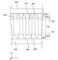
- FIG. 3 is an enlarged view of a main part of FIG.
- a region R1 that extends in the SAW propagation direction overlaps the dummy electrode 29, and a region that overlaps the gap between the dummy electrode 29 and the tip of the electrode finger 27. It is divided into R2, a region R3 overlapping the tip of the electrode finger 27, and a region R4 including the central portion of the intersecting region of the electrode fingers 27.
- the regions R1 to R4 are also divided along the propagation direction.
- the areas R1 to R4 may also be inclined together.
- the regions R1 to R4 are inclined with respect to the virtual lines. It becomes a parallelogram according to.
- Such an inclination angle may be, for example, 5 ° or more and 45 ° or less, although it depends on the Euler angle and the thickness of the piezoelectric layer 7. In the case of the above conditions, for example, the angle may be 25 ° or more and 35 ° or less. In this way, when the IDT electrode 19 is inclined by the imaginary line, the leakage of the transverse mode can be reduced.
- the dummy electrode 29 and the electrode finger 27 in the R1 region that is, the root of the electrode finger 27, the portion on the side connected to the bus bar 31.
- the line width of the connection part and the connection part side is sometimes thicker. That is, the electrode finger 27 includes the widened portion 27W. With such a configuration, the loss of the transverse mode is reduced.
- the line width is made thicker than the line width of the electrode finger 27 in the region R4 so as to continue from the region R1 to the regions R2 and R3 in the vicinity of the connection portion of the electrode finger 27. That is, the widened portion 27W continues to a position where it overlaps with the tip of the other electrode finger 27 when viewed in the arrangement direction of the electrode fingers 27.
- the line width is not thickened at the tip of the electrode finger 27 located in the region R3.
- the maximum phase (MaxPh) between fr and fa can be increased, and the acoustic wave element with less loss can be obtained. Can be provided. Further, since the phase can be reduced even on the higher frequency side than fa, it is possible to provide an elastic wave device with less loss.
- the Duty in the areas R1 to R3 is 1.05 times or more and 1.3 times or less than the Duty in the area R4.
- the Duty in the regions R1 to R3 may be 0.5 to 0.8.
- the length of the region R3 extending in the D2 direction may be, for example, 0.5 p or more and 2.5 p or less.
- the length of the region R4 extending in the D2 direction may be 65% or more of the intersecting width of the electrode fingers 27.
- the propagation angle ( ⁇ ) of the piezoelectric layer 7 is 90 °.
- the IDT electrode 19 was formed on the upper surface of the piezoelectric layer 7.
- the model of the electrode finger shape of the IDT electrode 19 according to Example 1 and Comparative Examples 1 to 3 is as shown in FIG.
- the base of the electrode finger 27 is thickened in the regions R1 to R3. Specifically, it is thicker from the tip of the dummy electrode 29 to 2 ⁇ m ahead.
- the electrode finger 27 and the dummy electrode 29 have the same thickness in all regions as the thickness of the electrode finger 27 of Example 1 in the region R4.
- the base of the electrode finger 27 is thickened to the same position as the tip of the dummy electrode 29. In other words, the entire region R1 is thickened.
- the base of the electrode finger 27 is thickened from the tip of the dummy electrode 29 to an inner position of 2 ⁇ m.
- how thick the root of the electrode finger 27 is made may be indicated as an offset amount based on the tip of the dummy electrode 29. That is, the offset amount is +2 ⁇ m in Example 1, 0 ⁇ m in Comparative Example 2, and ⁇ 2 ⁇ m in Comparative Example 3.
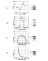
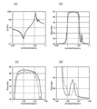
- FIG. 5A shows impedance characteristics
- FIG. 5B shows phase characteristics
- FIG. 5C shows an enlarged view near fr-fa in FIG. 5B
- FIG. 5C shows an enlarged view near fr-fa in FIG. 5B
- FIG. 5C shows an enlarged view near fr-fa in FIG. 5B
- FIG. 5C shows an enlarged view near fr-fa in FIG. 5B
- FIG. 5C shows an enlarged view near fr-fa in FIG. 5B
- FIG. 5C shows an enlarged view near fr-fa in FIG. 5B
- FIG. 5C shows an enlarged view near fr-fa in FIG. 5B
- FIG. 5C shows an enlarged view near fr-fa in FIG. 5B
- FIG. 5C shows an enlarged view near fr-fa in FIG. 5B
- FIG. 5C shows an enlarged view near fr-fa in FIG. 5B
- FIG. 5C shows an enlarged view near fr-fa in FIG. 5B
- Example 1 has improved phase characteristics as compared with Comparative Examples 1 to 3. Specifically, the overall phase level itself is improved, and the spurious phase between fr and fa is reduced. Further, it was confirmed that the phase can be reduced even on the high frequency side of fa.
- FIG. 6A shows the relationship between the offset amount and the resonance frequency fr
- FIG. 6B shows the relationship between the offset amount, df (fr-fa interval), and the maximum phase value.
- 7 is a diagram corresponding to FIG. 5
- FIG. 8 is a diagram corresponding to FIG.
- the acoustic wave device according to Example 2 has improved phase characteristics near fr-fa regardless of the propagation angle. Specifically, the overall phase level itself is improved, and the spurious phase between fr and fa is reduced. Further, it was confirmed that the phase can be reduced even on the high frequency side of fa.
- the propagation angle may be 90 ° when a higher resonance frequency is required, and the propagation angle may be 0 ° when a resonator having a small df is required to form a steep filter.
- the first electrode finger 27A and the second electrode finger 27B both have the widened portion 27W at the root, but only one of them may be provided.
- an acoustic wave device was produced in which the piezoelectric layer 7 had the same thickness as that of the above-described embodiment and the cut angle was different to obtain resonance at a frequency lower than that of the above-described example. That is, an elastic wave element in which the type of elastic wave used is not a plate wave as in the present application was manufactured, and the offset amount was changed to measure the characteristics. As a result, it has been confirmed that it is not necessary to provide the wide portion 27W extending to the R3 region as described above. From this, it was confirmed that the characteristic improvement by providing the wide portion 27W continuing to the R3 region as described above is an effect exhibited only when the plate wave of A1 mode is used.
- the wide portion 27W is provided in the above example, the same effect can be obtained by providing a thick film portion having a thickness thicker than other portions at the same position.
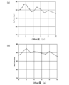
- FIG. 11 is a diagram showing how the maximum phase value changes with respect to the offset amount
- FIG. 11 (a) shows the result when a 106 ° Y rotation X propagation LT substrate is used as the piezoelectric layer 7.
- FIG. 11B shows the result when a Z rotation Y propagation LN substrate is used as the piezoelectric layer 7.
- the horizontal axis represents the offset amount and the vertical axis represents the maximum phase (unit: deg).
- the maximum phase value repeatedly increased and decreased as the offset amount was increased, and reached the maximum value when the offset amount was 2p regardless of the material of the piezoelectric layer 7. .. From the above, it was confirmed that the maximum phase can be increased when the offset amount is set to 1p to 3p. More preferably, the offset amount may be 1.5 p or more and 2.5 p or less.
- the gap interval (length of the region R2 in the D2 direction) is 0.3p. That is, it can be confirmed that it is important that the wide portion 27W extends from the region R1 to the region R2 and extends to the region R3.
- the frequency characteristic was measured when the line width of the widened portion 27W was changed with respect to the line width of the electrode finger 27 in the region R4. Specifically, the frequency characteristic was measured by changing the Duty in the region R4 to 0.35 to 0.5 and changing the Duty in the widened portion 27W in each Duty to the duty value in the region R4 to 0.75.
- the offset amount was 2p.
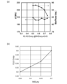
- FIG. 12 shows the result when the LT substrate is used as the piezoelectric layer 7.
- FIG. 12A is a diagram showing a relationship between the difference (df) between the resonance frequency and the anti-resonance frequency with respect to the duty of the widened portion 27W and the maximum phase value when the duty in the region R4 is 0.45. ..
- df difference between the resonance frequency and the anti-resonance frequency with respect to the duty of the widened portion 27W
- the maximum phase value when the duty in the region R4 is 0.45. ..
- FIG. 12B is a diagram showing a relationship between the Duty in the region R4 and a preferable value of the widened portion Duty.
- the duty in the region R4 when the duty in the region R4 is 0.45 or less, the duty of the widened portion 27W is 0.55, and when the duty in the region R4 is 0.5, the widened portion 27W.
- the duty of may be 0.6.
- the duty of the widened portion 27W may be a value obtained by adding 0.1 to the duty of the region R4 in order to increase the maximum phase value and secure df.
- the duty in the region R4 is 0.45 or less
- the duty of the widened portion 27W is 0.50 to 0.60
- the duty in the region R4 is 0.5 or more.
- the duty of the widened portion 27W may be a value obtained by adding 0.5 to 1.5 to the duty of the region R4.
- FIG. 13 shows a diagram corresponding to FIG. 12 when an LN substrate is used as the piezoelectric layer 7.
- the piezoelectric layer 7 is an LN substrate, there is no threshold value at which df changes greatly, so a preferable value was obtained as the maximum phase value.
- the duty in the region R4 is 0.45 or less
- the duty of the widened portion 27W is 0.50 to 0.60
- the duty in the region R4 is 0.5 or more
- the duty of the widened portion 27W is It may be a value obtained by adding 0.1 to the duty of the region R4.
- the maximum phase value changes in a quadratic function across the maximum value, so the characteristics can be maintained within a range of about 0.1 across the maximum value. Therefore, when the duty in the region R4 is 0.45 or less, the duty of the widened portion 27W is 0.50 to 0.60, and when the duty in the region R4 is 0.5 or more, the duty of the widened portion 27W is the region R4. It may be a value obtained by adding 0.5 to 1.5 to the duty of.
- the elastic wave device 1A shown in FIG. 14 has a membrane shape in which the piezoelectric layer 7 is arranged on the substrate 3 having the recess 3x. Even in this case, if a plate wave is used, the same effect can be obtained.
- FIG. 15 shows a frequency characteristic of the acoustic wave device 1A as a solid line as a third embodiment.
- frequency characteristics of an elastic wave device having the same configuration as that of the elastic wave device 1A except that the wide portion 27A is not provided are indicated by broken lines in FIG. 15 (a) to 15 (d) are diagrams corresponding to FIGS. 5 (a) to 5 (d).
- the maximum phase value can be increased even in the elastic wave device 1A in the form of a membrane that does not have a multilayer film.
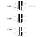
- the electrode fingers 27 were shaped as in Examples 4, 5 and Comparative Example 8 shown in FIG. Specifically, the fourth embodiment has the same shape as that of the first embodiment, and the fifth embodiment is such that, in the electrode finger shape of the fourth embodiment, the tip portion of the electrode finger 27 located in the region R3 is also a wide portion. In Comparative Example 8, only the tip end portion of the electrode finger 27 located in the region R3 has the wide portion, and the other portions have the same electrode finger width as the region R4.
- FIGS. 17A to 17D are diagrams corresponding to FIGS. 5A to 5D.
- Example 4 is shown by a solid line
- Example 5 is shown by a broken line with a long interval
- Comparative Example 8 is shown by a broken line with a short interval.
- Example 4 Compared Example 4 and Example 5, in Example 5, compared with Example 4, the characteristics were slightly improved on the higher frequency side than fa, but the spurious between fr and fa was slightly. It was confirmed that spurious was generated on the frequency side lower than fr as the frequency increased.
- the width of the wide portion 27W may be uniform in the regions R1 to R3. In this case, since the protrusion protruding in the propagation direction of the elastic wave is not provided, it is possible to reduce the risk that the electrode fingers are short-circuited. (Application example of elastic wave device: duplexer)
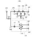
- FIG. 9 is a circuit diagram schematically showing the configuration of the demultiplexer 101 as an example of using the elastic wave device 1. As can be understood from the reference numerals shown in the upper left of the drawing, the comb-teeth electrode 23 and the reflector 21 are simplified in this figure.
- the demultiplexer 101 filters, for example, a transmission signal from the transmission terminal 105 and outputs it to the antenna terminal 103, and a reception signal from the antenna terminal 103 and outputs it to a pair of reception terminals 107. It has a reception filter 111.
- the transmission filter 109 is composed of, for example, a ladder type filter in which a plurality of resonators 15 are connected in a ladder type. That is, the transmission filter 109 connects a plurality (or one) of the resonators 15 connected in series between the transmission terminal 105 and the antenna terminal 103, the series line (series arm) thereof, and the reference potential. And a plurality of (even one may be) resonators 15 (parallel arms).
- the plurality of resonators 15 that form the transmission filter 109 are provided, for example, on the same fixed substrate 2 (3, 5, and 7).
- the reception filter 111 includes, for example, a resonator 15 and a multimode filter (including a double mode filter) 113.
- the multimode filter 113 has a plurality of (three in the illustrated example) IDT electrodes 19 arranged in the propagation direction of the elastic wave, and a pair of reflectors 21 arranged on both sides thereof.
- the resonator 15 and the multimode filter 113 that form the reception filter 111 are provided on the same fixed substrate 2, for example.
- the transmission filter 109 and the reception filter 111 may be provided on the same fixed substrate 2 or different fixed substrates 2.
- FIG. 9 is merely an example of the configuration of the demultiplexer 101.
- the reception filter 111 may be a ladder type filter like the transmission filter 109.
- the demultiplexer 101 includes the transmission filter 109 and the reception filter 111 has been described, but the demultiplexer 101 is not limited to this. For example, it may be a diplexer or a multiplexer including three or more filters.
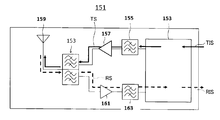
- FIG. 10 is a block diagram showing a main part of a communication device 151 as a usage example of the elastic wave device 1 (branching filter 101).
- the communication device 151 performs wireless communication using radio waves and includes the duplexer 101.
- the transmission information signal TIS including the information to be transmitted is modulated by the RF-IC (Radio Frequency Integrated Circuit) 153 and the frequency is raised (conversion of the carrier frequency to a high frequency signal) to form a transmission signal TS.
- the transmission signal TS has unnecessary components other than the transmission pass band removed by the band pass filter 155, is amplified by the amplifier 157, and is input to the demultiplexer 101 (transmission terminal 105). Then, the demultiplexer 101 (transmission filter 109) removes unnecessary components other than the transmission pass band from the input transmission signal TS, and outputs the removed transmission signal TS from the antenna terminal 103 to the antenna 159.
- the antenna 159 converts the input electric signal (transmission signal TS) into a radio signal (radio wave) and transmits it.
- the radio signal (radio wave) received by the antenna 159 is converted into an electric signal (received signal RS) by the antenna 159 and input to the duplexer 101 (antenna terminal 103).
- the demultiplexer 101 removes unnecessary components other than the reception pass band from the input reception signal RS and outputs the reception signal RS from the reception terminal 107 to the amplifier 161.
- the output reception signal RS is amplified by the amplifier 161, and unnecessary components other than the reception pass band are removed by the band pass filter 163.
- the reception signal RS is subjected to frequency reduction and demodulation by the RF-IC 153 to be a reception information signal RIS.
- the transmission information signal TIS and the reception information signal RIS may be low-frequency signals (baseband signals) containing appropriate information, and are, for example, analog voice signals or digitized voice signals.
- the pass band of the radio signal may be set appropriately, and in the present embodiment, a pass band of relatively high frequency (for example, 5 GHz or more) is also possible.
- the modulation method may be phase modulation, amplitude modulation, frequency modulation, or a combination of two or more of these.
- the direct conversion method is illustrated in FIG. 17 as the circuit method, any other suitable circuit method may be used, and for example, a double superheterodyne method may be used.
- FIG. 10 schematically shows only a main part, and a low-pass filter, an isolator or the like may be added at an appropriate position, or the position of the amplifier or the like may be changed.
- the present disclosure is not limited to the above embodiments and may be implemented in various modes.
- the thickness of each layer and the Euler angle of the piezoelectric layer may be values outside the ranges exemplified in the embodiment.
Landscapes
- Physics & Mathematics (AREA)
- Acoustics & Sound (AREA)
- Surface Acoustic Wave Elements And Circuit Networks Thereof (AREA)
Abstract
電極指のピッチに対して相対的に周波数が高い共振を実現できる弾性波装置を提供する。弾性波装置1は、基板3と、基板3上に位置している多層膜5と、多層膜5上に位置している、圧電層7と、圧電層7上に位置しているIDT電極19と、IDT電極19の電極指27の太さは、バスバーに接続された部位から、電極指27の配列方向でみたときに他方の電極指27の先端と重なる位置まで太くなっている。
Description
本開示は、弾性波を利用する弾性波装置、当該弾性波装置を含む分波器および通信装置に関する。
圧電体上のIDT(interdigital transducer)電極に電圧を印加して、圧電体を伝搬する弾性波を生じさせる弾性波装置が知られている。IDT電極は、1対の櫛歯電極を有している。1対の櫛歯電極は、それぞれ複数の電極指を有しており、互いに噛み合うように配置される。弾性波装置においては、電極指のピッチの2倍を波長とする弾性波の定在波が形成され、この定在波の周波数が共振周波数となる。
近年、弾性波のうち板波を用いる弾性波装置が提案されている。このような弾性波装置として、基板と、基板上に位置している音響反射層と、音響反射層上に位置している圧電体層と、圧電体層上に位置しているIDT電極とを有する構成が提案されている。音響反射層は、低音響インピーダンス層と高音響インピーダンス層とを交互に積層して構成されている。このような構成により、電極指の周期が3μm程度であっても5GHzに共振点を有する弾性波装置を提供することができる。
電極指のピッチに対して相対的に周波数が高い共振を実現できる弾性波装置、分波器および通信装置が提供されることが望まれる。
本開示の一態様に係る弾性波装置は、圧電層と、前記圧電層上に位置しているIDT電極と、を有している。前記IDT電極は、互いに異なる電位に接続され、互いに間隔を開けて配置された第1バスバーおよび第2バスバーと、弾性波伝搬方向に沿って交互に配列された、前記第1バスバーに接続され前記第2バスバー側に延びる第1電極指および前記第2バスバーに接続され前記第1バスバー側に延びる第2電極指と、を含む。前記第1電極指は、前記第1バスバーに接続される部分から、前記第1電極指と前記第2電極指との配列方向でみたときに前記第2電極指の先端と重複する位置までの太さが、前記第1電極指と前記第2電極指との交差領域の中央付近に比べて太くなっている拡幅部を備える。前記圧電層の厚さは、前記IDT電極の電極指のピッチをpとしたときに1.5p未満である。
本開示の一態様に係る弾性波装置は、圧電層と、前記圧電層上に位置しているIDT電極と、を有するA1モードの板波を用いるものである。前記IDT電極は、互いに異なる電位に接続され、互いに間隔を開けて配置された第1バスバーおよび第2バスバーと、弾性波伝搬方向に沿って交互に配列された、前記第1バスバーに接続され前記第2バスバー側に延びる第1電極指および前記第2バスバーに接続され前記第1バスバー側に延びる第2電極指と、を含む。前記第1電極指は、前記第1バスバーに接続される部分から、前記第1電極指と前記第2電極指との配列方向でみたときに前記第2電極指の先端と重複する位置までの太さが、前記第1電極指と前記第2電極指との交差領域の中央付近に比べて太くなっている拡幅部を備える。
本開示の一態様に係る分波器は、アンテナ端子と、前記アンテナ端子へ出力される信号をフィルタリングする送信フィルタと、前記アンテナ端子から入力される信号をフィルタリングする受信フィルタと、を有しており、前記送信フィルタおよび前記受信フィルタの少なくとも一方が上記の弾性波装置を含んでいる。
本開示の一態様に係る通信装置は、アンテナと、前記アンテナに前記アンテナ端子が接続されている上記の分波器と、前記送信フィルタおよび前記受信フィルタに対して信号経路に関して前記アンテナ端子とは反対側に接続されているICと、を有している。
上記の構成によれば、電極指のピッチに対して相対的に周波数が高い共振を実現できる。
以下、本開示に係る実施形態について、図面を参照して説明する。なお、以下の説明で用いられる図は模式的なものであり、図面上の寸法比率等は現実のものとは必ずしも一致していない。
本開示に係る弾性波装置は、いずれの方向が上方または下方とされてもよいものであるが、以下では、便宜的に、D1軸、D2軸およびD3軸からなる直交座標系を定義するとともに、D3軸の正側を上方として、上面または下面等の用語を用いることがある。また、平面視または平面透視という場合、特に断りがない限りは、D3軸方向に見ることをいう。なお、D1軸は、後述する圧電層の上面に沿って伝搬する弾性波の伝搬方向に平行になるように定義され、D2軸は、圧電層の上面に平行かつD1軸に直交するように定義され、D3軸は、圧電層の上面に直交するように定義されている。
(弾性波装置の全体構成)
図1は、弾性波装置1の要部の構成を示す平面図である。図1は後述する共振子の構成を示している。図2は、図1のII-II線における断面図である。
図1は、弾性波装置1の要部の構成を示す平面図である。図1は後述する共振子の構成を示している。図2は、図1のII-II線における断面図である。
弾性波装置1は、例えば、基板3(図2)と、基板3上に位置する多層膜5(図2)と、多層膜5上に位置する圧電層7と、圧電層7上に位置する導電層9とを有している。各層は、例えば、概ね一定の厚さとされている。なお、基板3、多層膜5および圧電層7の組み合わせを固着基板2(図2)ということがある。
弾性波装置1では、導電層9に電圧が印加されることによって、圧電層7を伝搬する弾性波が励振される。弾性波装置1は、例えば、この弾性波を利用する共振子および/またはフィルタを構成している。多層膜5は、例えば、弾性波を反射して弾性波のエネルギーを圧電層7に閉じ込めることに寄与している。基板3は、例えば、多層膜5および圧電層7の強度を補強することに寄与している。
弾性波装置1は、図1に示す共振子単独であってもよいし、共振子を複数備えてフィルタ等を構成してもよい。
(固着基板の概略構成)
基板3は、直接的には、弾性波装置1の電気的特性に影響しない。従って、基板3の材料および寸法は適宜に設定されてよい。基板3の材料は、例えば、絶縁材料であり、絶縁材料は、例えば、樹脂またはセラミックである。なお、基板3は、圧電層7等に比較して熱膨張係数が低い材料によって構成されていてもよい。この場合、例えば、温度変化によって弾性波装置1の周波数特性が変化してしまう虞を低減することができる。このような材料としては、例えば、シリコン等の半導体、サファイア等の単結晶および酸化アルミニウム質焼結体等のセラミックを挙げることができる。なお、基板3は、互いに異なる材料からなる複数の層が積層されて構成されていてもよい。基板3の厚さは、例えば、圧電層7よりも厚い。
基板3は、直接的には、弾性波装置1の電気的特性に影響しない。従って、基板3の材料および寸法は適宜に設定されてよい。基板3の材料は、例えば、絶縁材料であり、絶縁材料は、例えば、樹脂またはセラミックである。なお、基板3は、圧電層7等に比較して熱膨張係数が低い材料によって構成されていてもよい。この場合、例えば、温度変化によって弾性波装置1の周波数特性が変化してしまう虞を低減することができる。このような材料としては、例えば、シリコン等の半導体、サファイア等の単結晶および酸化アルミニウム質焼結体等のセラミックを挙げることができる。なお、基板3は、互いに異なる材料からなる複数の層が積層されて構成されていてもよい。基板3の厚さは、例えば、圧電層7よりも厚い。
多層膜5は、低音響インピーダンス層11と高音響インピーダンス層13とを交互に積層することにより構成されている。これにより、両者の界面においては弾性波の反射率が比較的高くなる。その結果、例えば、圧電層7を伝搬する弾性波の厚み方向への漏れが低減される。なお、低音響インピーダンス層11を構成する材料としては、二酸化ケイ素(SiO2)を例示できる。高音響インピーダンス層13を構成する材料としては、五酸化タンタル(Ta2O5)や酸化ハフニウム(HfO2)、酸化ジルコニウム(ZrO2)、酸化チタン(TiO2)を例示できる。
多層膜5の積層数は適宜に設定されてよい。例えば、多層膜5は、低音響インピーダンス層11および高音響インピーダンス層13の合計の積層数が2層以上12層以下とされてよい。多層膜5の合計の積層数は、偶数でもよいし、奇数でもよいが、圧電層7に接する層は、低音響インピーダンス層11である。基板3に接する層については、低音響インピーダンス層11,高音響インピーダンス層13のいずれであってもよい。また、各層の間や、基板3と多層膜5との間、もしくは多層膜5と圧電層7との間に、密着や拡散防止を目的に付加膜を挿入してもよい。その場合には、付加膜は弾性波装置1の特性に影響を与えない程度に薄く(概ね0.01λ以下)してもよい。
圧電層7は、タンタル酸リチウム(LiTaO3、以下、LTという)やニオブ酸リチウム(LiNbO3、以下、LNという)の単結晶によって構成されている。
圧電層7としてLTを用いる場合には、カット角は、例えば、オイラー角(φ,θ,ψ)で(0°±10°,0°以上55°以下,0°±10°)である。別の観点では、LTは、回転YカットX伝搬のものであり、Y軸は、圧電層7の法線(D3軸)に対して90°以上145°の角度で傾斜している。X軸は、圧電層7の上面(D1軸)に概ね平行である。ただし、X軸とD1軸とは、XZ平面またはD1D2平面において-10°以上10°以下で傾斜していてもよい。
圧電層7としてLNを用いる場合には、オイラー角で(0°±10°,0°±15°,ψ)、ただしψは0°~360°とする。また、(0°±5°,0°±5°,ψ)としてもよい。別の観点では、Zカット基板としてもよい。
また、圧電層7の厚さは、比較的薄くされており、例えば、後述するλを基準として、0.75λ以下である。より具体的には、0.15λ以上0.3λ以下である。圧電層7のカット角および厚さをこのように設定することにより、弾性波として、A1モードの板波に近い振動モードのものを利用することが可能になる。
以下、本実施形態においては圧電層7としてLNを用いた場合を例に説明するものとする。
(導電層の概略構成)
導電層9は、例えば、金属により形成されている。金属は、適宜な種類のものとされてよく、例えば、アルミニウム(Al)またはAlを主成分とする合金(Al合金)である。Al合金は、例えば、Al-銅(Cu)合金である。なお、導電層9は、複数の金属層から構成されていてもよい。また、AlまたはAl合金と、圧電層7との間に、これらの接合性を強化するためのチタン(Ti)からなる比較的薄い層が設けられていてもよい。
導電層9は、例えば、金属により形成されている。金属は、適宜な種類のものとされてよく、例えば、アルミニウム(Al)またはAlを主成分とする合金(Al合金)である。Al合金は、例えば、Al-銅(Cu)合金である。なお、導電層9は、複数の金属層から構成されていてもよい。また、AlまたはAl合金と、圧電層7との間に、これらの接合性を強化するためのチタン(Ti)からなる比較的薄い層が設けられていてもよい。
導電層9は、図1の例では、共振子15を構成するように形成されている。共振子15は、いわゆる1ポート弾性波共振子として構成されており、概念的かつ模式的に示す端子17Aおよび17Bの一方から所定の周波数の電気信号が入力されると共振を生じ、その共振を生じた信号を端子17Aおよび17Bの他方から出力可能である。
導電層9(共振子15)は、例えば、IDT電極19と、IDT電極19の両側に位置する1対の反射器21とを含んでいる。
IDT電極19は、互いに異なる電位に接続される1対の櫛歯電極23(第1櫛歯電極23A,第2櫛歯電極23B)を含んでいる。各櫛歯電極23は、例えば、バスバー25(第1バスバー25A,第2バスバー25B)と、バスバー25から互いに並列に延びる複数の電極指27(第1電極指27,第2電極指27B)と、複数の電極指27間においてバスバー25から突出するダミー電極29(第1ダミー電極29A,第2ダミー電極29B)とを含んでいる。1対の櫛歯電極23は、複数の電極指27が互いに噛み合うように(交差するように)配置されている。
なお、以後、第1櫛歯電極23Aと第2櫛歯電極23Bとに共通する説明するでは単に櫛歯電極23という。他の構成要素についても同様である。
バスバー25は、例えば、概ね一定の幅で弾性波の伝搬方向(D1軸方向)に直線状に延びる長尺状に形成されている。そして、一対のバスバー25は、弾性波の伝搬方向に直交する方向(D2軸方向)において互いに対向している。なお、バスバー25は、幅が変化したり、弾性波の伝搬方向に対して傾斜したりしていてもよい。
各電極指27は、例えば、概ね一定の幅で弾性波の伝搬方向に直交する方向(D2軸方向)に直線状に延びる長尺状に形成されている。各櫛歯電極23において、複数の電極指27は、弾性波の伝搬方向に配列されている。また、一方の櫛歯電極23の複数の電極指27と他方の櫛歯電極23の複数の電極指27とは、基本的には交互に配列されている。
複数の電極指27のピッチp(例えば互いに隣り合う2本の電極指27の中心間距離)は、IDT電極19内において基本的に一定である。なお、IDT電極19の一部に、他の大部分よりもピッチpが狭くなる狭ピッチ部、または他の大部分よりもピッチpが広くなる広ピッチ部が設けられてもよい。
なお、以下において、ピッチpという場合、特に断りがない限りは、上記のような狭ピッチ部または広ピッチ部のような特異な部分を除いた部分(複数の電極指27の大部分)のピッチをいうものとする。また、特異な部分を除いた大部分の複数の電極指27においても、ピッチが変化しているような場合においては、大部分の複数の電極指27のピッチの平均値をピッチpの値として用いてよい。「大部分」とは、例えば、電極指27全体の80%以上を言うものとする。
複数の電極指27の長さは、例えば、互いに同等である。なお、IDT電極19は、複数の電極指27の長さ(別の観点では交差幅)が伝搬方向の位置に応じて変化する、いわゆるアポダイズが施されていてもよい。
ダミー電極29は、例えば、概ね一定の幅で弾性波の伝搬方向に直交する方向に突出している。また、一方の櫛歯電極23のダミー電極29の先端は、他方の櫛歯電極23の電極指27の先端とギャップを介して対向している。なお、IDT電極19は、ダミー電極29を含まないものであってもよい。
1対の反射器21は、弾性波の伝搬方向において複数のIDT電極19の両側に位置している。各反射器21は、例えば、格子状に形成されている。すなわち、反射器21は、互いに対向する1対のバスバー31と、1対のバスバー31間において延びる複数のストリップ電極33とを含んでいる。複数のストリップ電極33のピッチ、および互いに隣接する電極指27とストリップ電極33とのピッチは、基本的には複数の電極指27のピッチと同等である。
そして、圧電層7の上面は導電層9の上から保護膜37によって覆われていてもよい。保護膜37は、圧電層7よりも音速の遅い材料で構成する。そのような材料としては例えば、SiO2やSi3N4,Si等がある。保護膜37は、導電層9直上のみに設けてもよいし、導電層9で構成される電極指27間にも設けてもよい。保護膜37を電極指27間にも設ける場合には、保護膜37を絶縁材料としてもよい。また、保護膜37はこれらの材料からなる複数層の積層体としてもよい。
また、保護膜37は、単に導電層9の腐食を抑制するためのものであってもよいし、温度補償に寄与するものであってもよい。導電層9と保護膜37との音響的境界を明瞭にするために、IDT電極19および反射器21の上面または下面には、弾性波の反射係数を向上させるために、絶縁体または金属からなる付加膜が設けられてもよい。
図1および図2に示した構成は、適宜にパッケージされてよい。パッケージは、例えば、不図示の実装基板上に隙間を介し圧電層7の上面を対向させるように図示の構成を実装し、その上から樹脂封止するものであってもよいし、圧電層7上に箱型のカバーを設けるウェハレベルパッケージ型のものであってもよい。
(A1モード板波の利用)
1対の櫛歯電極23に電圧が印加されると、複数の電極指27によって圧電層7に電圧が印加され、圧電体である圧電層7が振動する。これにより、D1軸方向に伝搬する弾性波が励振される。弾性波は、複数の電極指27によって反射される。そして、複数の電極指27のピッチpを概ね半波長(λ/2)とする定在波が立つ。定在波によって圧電層7に生じる電気信号は、複数の電極指27によって取り出される。このような原理により、弾性波装置1は、ピッチpを半波長とする弾性波の周波数を共振周波数とする共振子として機能する。なお、λは、通常、波長を示す記号であり、また、実際の弾性波の波長は2pからずれることもあるが、以下でλの記号を用いる場合、特に断りがない限り、λは2pを意味するものとする。
1対の櫛歯電極23に電圧が印加されると、複数の電極指27によって圧電層7に電圧が印加され、圧電体である圧電層7が振動する。これにより、D1軸方向に伝搬する弾性波が励振される。弾性波は、複数の電極指27によって反射される。そして、複数の電極指27のピッチpを概ね半波長(λ/2)とする定在波が立つ。定在波によって圧電層7に生じる電気信号は、複数の電極指27によって取り出される。このような原理により、弾性波装置1は、ピッチpを半波長とする弾性波の周波数を共振周波数とする共振子として機能する。なお、λは、通常、波長を示す記号であり、また、実際の弾性波の波長は2pからずれることもあるが、以下でλの記号を用いる場合、特に断りがない限り、λは2pを意味するものとする。
ここで、上述のように、圧電層7は、比較的薄くされ、かつそのオイラー角が(0°±10°,0°±15°,0°±10°)とされていることから、弾性波装置1はA1モードの板波の弾性波を利用可能になっている。A1モードの弾性波の伝搬速度(音速)は、一般的なSAW(Surface Acoustic Wave)の伝搬速度よりも速い。例えば、一般的なSAWの伝搬速度が3000~4000m/sであるのに対して、A1モードの弾性波の伝搬速度は10000m/s以上である。従って、従来と同等のピッチpで、従来よりも高周波領域での共振を実現することができる。例えば、1μm以上のピッチpで5GHz以上の共振周波数を実現することができる。
(各層の材料および厚さの設定)
A1モードの弾性波を利用して比較的高い周波数領域(例えば5GHz以上)の共振を実現するためには、多層膜5の材料および厚さ、圧電体層(本実施形態では圧電層7)のオイラー角、材料および厚さ、ならびに導電層9の厚さの組み合わせに条件がある。
A1モードの弾性波を利用して比較的高い周波数領域(例えば5GHz以上)の共振を実現するためには、多層膜5の材料および厚さ、圧電体層(本実施形態では圧電層7)のオイラー角、材料および厚さ、ならびに導電層9の厚さの組み合わせに条件がある。
例えば、以下の条件としたときに、共振周波数および反共振周波数近傍にスプリアスが存在しない状態で5GHzの共振を得ることができた。
圧電層:
材料:LN
厚さ:0.19λ
オイラー角:(0,0,0)
多層膜:
材料:2種(SiO2,Ta2O5)
厚み:SiO2層 0.10λ,Ta2O5層 0.07λ
積層数:8層
導電層:
材料:Al
厚さ:0.06λ
ピッチp:1μm(λ=2μm)
材料:LN
厚さ:0.19λ
オイラー角:(0,0,0)
多層膜:
材料:2種(SiO2,Ta2O5)
厚み:SiO2層 0.10λ,Ta2O5層 0.07λ
積層数:8層
導電層:
材料:Al
厚さ:0.06λ
ピッチp:1μm(λ=2μm)
なお、多層膜5の積層数は、2種の層の数の合計(例えば図2の例では4)である。また、ピッチpは1μmであるが、ピッチを変化させた場合も、λ=2pで表される波長にしたがって実際の膜厚を変化させれば、共振特性は周波数依存性が全体的にシフトするだけで同様の結果となる。すなわち、波長またはピッチで規格化した場合も同様の結果を得ることができる。
上記の例の他にも、例えば、以下の条件としたときにピッチが0.9μm~1.4μmの場合であっても、5GHz以上の共振を得ることができ、かつ、共振周波数および反共振周波数近傍にリップルのない状態を得ることができた。なお、以下の条件は、圧電層7の材料、圧電層7の厚み、低音響インピーダンス層11の材料、厚み、高音響インピーダンス層13の材料、厚みの順に各条件を“/”で区切って示している。
他条件1:LN/0.2λ/SiO2/0.06λ/HfO2/0.095λ
他条件2:LT/0.175λ/SiO2/0.09λ/Ta2O5/0.07λ
他条件3:LT/0.2λ/SiO2/0.1λ/HfO2/0.08λ
なお、他条件2,3のときに、LTのオイラー角は(0°±5°,24°±5°,0°±5°)もしくは(0°±5°,16°±5°,0°±5°)である。
他条件2:LT/0.175λ/SiO2/0.09λ/Ta2O5/0.07λ
他条件3:LT/0.2λ/SiO2/0.1λ/HfO2/0.08λ
なお、他条件2,3のときに、LTのオイラー角は(0°±5°,24°±5°,0°±5°)もしくは(0°±5°,16°±5°,0°±5°)である。
(電極指構造)
弾性波装置1において、A1モード板波を用いたときには、圧電層7の厚みが20μm程度ある通常の弾性波装置に比べて共振周波数(fr)と反共振周波数(fa)との間のインピーダンス特性が悪い傾向があった。これは圧電層7の厚みが薄くなることにより顕著になる。
弾性波装置1において、A1モード板波を用いたときには、圧電層7の厚みが20μm程度ある通常の弾性波装置に比べて共振周波数(fr)と反共振周波数(fa)との間のインピーダンス特性が悪い傾向があった。これは圧電層7の厚みが薄くなることにより顕著になる。
これに対して、弾性波装置1は電極指27の太さを変化させている。図3は、図1の要部拡大図である。図3に示すように、SAWの伝搬方向(すなわち電極指27の繰り返し配列方向,D1方向)に伸びる、ダミー電極29と重なる領域R1、ダミー電極29と電極指27の先端とのギャップと重なる領域R2、電極指27の先端と重なる領域R3、電極指27の交差領域の中央部を含む領域R4と区分する。なお、この例では電極指27の交差領域は伝搬方向と平行であるため、各領域R1~R4も伝搬方向に沿って区分したが、IDT電極19がアポタイズされていたり傾斜していたりする場合には各領域R1~R4も合せて傾斜させればよい。例えば、電極指27の交差幅は略同一で、電極指27の先端を結ぶ仮想線が電極指27の繰り返し配列方向に対して傾斜している場合には、領域R1~R4は仮想線の傾斜にあわせた平行四辺形となる。このような傾斜角度は圧電層7のオイラー角,厚み等にもよるが、例えば5°以上45°以下を例示できる。上記条件の場合には例えば、25°以上35°以下としてもよい。このようにIDT電極19の仮想線傾斜させた場合には横モードの漏洩を低減することができる。
まず、領域R4の電極指27の線幅(D1方向における幅)に比べ、R1領域のダミー電極29および電極指27(すなわち電極指27の根元,バスバー31と接続される側の部分。以下、単に接続部,接続部側ということがある)の線幅を太くしている。すなわち、電極指27は拡幅部27Wを備えている。このような構成とすることで、横モードのロスを低減する。
さらに、本例では、電極指27の接続部近傍で、領域R1から領域R2,R3まで続くように、線幅を領域R4の電極指27の線幅に比べて太くしている。すなわち、拡幅部27Wは電極指27の配列方向でみたときに、他方の電極指27の先端と重なる位置まで続いている。なお、領域R3に位置する電極指27の先端部においては線幅を太らせていない。
このように、領域R3まで電極指27の接続部側を太らせること(拡幅部27Wとすること)で、fr-fa間の最大位相(MaxPh)を高めることができ、ロスの少ない弾性波素子を提供することができる。また、faよりも高周波数側においても位相を小さくすることができるので、ロスの少ない弾性波装置を提供することができる。
例えば、領域R1~R3におけるDutyは、領域R4におけるDutyの1.05倍以上1.3倍以下である。具体的には領域R1~R3におけるDutyは、0.5~0.8としてもよい。
また、領域R3のD2方向に伸びる長さは、例えば、0.5p以上2.5p以下としてもよい。領域R4のD2方向に延びる長さは電極指27の交差幅の65%以上としてもよい。
上述の効果を実測値で検証した。圧電層7の伝搬角(ψ)は90°としている。このような圧電層7の上面にIDT電極19を形成した。実施例1,比較例1~3にかかるIDT電極19の電極指形状のモデルは、図4に示す通りとした。実施例1に係る弾性波素子1は電極指27の根元が領域R1~R3まで太くなっている。具体的には、ダミー電極29の先端から2μm先まで太くなっている。比較例1は、電極指27およびダミー電極29が全領域において実施例1の電極指27の領域R4における太さと同じ太さとしている。比較例2は、電極指27の根元をダミー電極29の先端と同じ位置まで太くしている。言い換えると、領域R1の全領域において太くしている。比較例3は、電極指27の根元を、ダミー電極29の先端から2μmの内側の位置まで太くしている。なお、以下の説明において、電極指27の根元をどこまで太くするかを、ダミー電極29の先端を基準としたオフセット量として示すことがある。すなわち、オフセット量は、実施例1は+2μmであり、比較例2は0μm、比較例3は―2μmである。
実施例1,比較例1~3の周波数特性を測定した結果を図5に示す。図5(a)はインピーダンス特性を示し、図5(b)は位相特性を示し、図5(c)に図5(b)のfr-fa付近の拡大図を示し、図5(d)に図5(b)のfaの高周波数側の拡大図を示す。図5において、横軸は規格化周波数であり、縦軸は、図5(a)はインピーダンスであり、図5(b)~図5(d)は位相である。
図5から明らかなように、fr-fa付近において、実施例1は比較例1~3に比べて位相特性が向上している。具体的には、全体的な位相レベル自体が向上している上に、fr-fa間の位相のスプリアスも少なくなっている。さらに、faの高周波数側においても位相を小さくできることが確認できた。
さらに、図6(a)に、オフセット量と共振周波数frとの関係を、図6(b)にオフセット量とdf(fr-fa間隔),最大位相値との関係をそれぞれ示す。図6からも明らかなように、オフセット量を大きくするにつれて、dfを維持したまま、最大位相を大きくすることができることを確認した。
なお、実施例2,比較例4~6として、圧電層7の伝搬角をψ=0°とした場合の結果について、図7,図8に示す。図7は図5に相当する図であり、図8は図6に相当する図である。
この図からも明らかように、伝搬角に関係なく、実施例2に係る弾性波素子は、fr-fa付近において位相特性が向上している。具体的には、全体的な位相レベル自体が向上している上に、fr-fa間の位相のスプリアスも少なくなっている。さらに、faの高周波数側においても位相を小さくできることが確認できた。
また、図8から明らかなように、伝搬角が0°の場合にも、オフセット量を大きくするにつれて最大位相が大きくなる様子を確認した。
以上の結果から、より高い共振周波数が必要な場合には伝搬角を90°とし、急峻なフィルタを形成するためにdfの小さい共振子が必要な場合には伝搬角を0°としてもよい。
なお、上述の例では、第1電極指27Aおよび第2電極指27B共に根元に拡幅部27Wを備える構成としたが、一方のみでもよい。
また、比較例として、圧電層7の厚みを上述の実施形態と同様にし、カット角を異ならせることで、上述の実施例よりも低い周波数の共振を得るような弾性波素子を製造した。すなわち、利用する弾性波の種類が本願のような板波ではない弾性波素子を製造し、オフセット量を変化させて特性を測定した。その結果、上述のようにR3領域まで続く幅広部27Wを設ける必要はないことを確認している。このことから、上述のようにR3領域まで続く幅広部27Wを備えることによる特性向上はA1モードの板波を用いた場合のみに発現する効果であることが確認された。
また、上述の例では、幅広部27Wを設けたが、同じ位置において、他の部位に比べて厚みの厚い厚膜部を設けることでも同様の効果を得られる。
(オフセット量)
次に、オフセット量の範囲を確認した。具体的には、ピッチpに対するオフセット量をピッチp比で0~10まで変化させたときの周波数特性を測定した。その結果を図11に示す。図11はオフセット量に対する最大位相値の変化の様子を示す線図であり、図11(a)は、圧電層7として、106°Y回転X伝搬のLT基板を用いた場合の結果を示し、図11(b)は、圧電層7として、Z回転Y伝搬のLN基板を用いた場合の結果を示す。
次に、オフセット量の範囲を確認した。具体的には、ピッチpに対するオフセット量をピッチp比で0~10まで変化させたときの周波数特性を測定した。その結果を図11に示す。図11はオフセット量に対する最大位相値の変化の様子を示す線図であり、図11(a)は、圧電層7として、106°Y回転X伝搬のLT基板を用いた場合の結果を示し、図11(b)は、圧電層7として、Z回転Y伝搬のLN基板を用いた場合の結果を示す。
図11において、横軸はオフセット量、縦軸は最大位相(単位:deg)を示している。図11からも明らかなように、オフセット量を増やすに従い最大位相値は周期的に増減を繰り返し、圧電層7の材料によらず、オフセット量が2pのときに最大値をとる様子が確認された。以上より、オフセット量を1p~3pにしたときには最大位相を高くすることができることを確認した。より好ましくは、オフセット量を1.5p以上2.5p以下としてもよい。
なお、ギャップ間隔(領域R2のD2方向の長さ)は0.3pとしている。すなわち、幅広部27Wは、領域R1から領域R2を超え、領域R3まで延びることが重要であることを確認できる。
(拡幅量)
領域R4における電極指27の線幅に対して、拡幅部27Wの線幅を変化させたときの周波数特性を測定した。具体的には、領域R4におけるDutyを0.35~0.5に、各Dutyにおいて、拡幅部27WにおけるDutyを領域R4におけるDutyの値~0.75まで変化させて周波数特性を測定した。なお、オフセット量は2pとした。
領域R4における電極指27の線幅に対して、拡幅部27Wの線幅を変化させたときの周波数特性を測定した。具体的には、領域R4におけるDutyを0.35~0.5に、各Dutyにおいて、拡幅部27WにおけるDutyを領域R4におけるDutyの値~0.75まで変化させて周波数特性を測定した。なお、オフセット量は2pとした。
圧電層7としてLT基板を用いた場合の結果を、図12に示す。図12(a)は領域R4におけるDutyを0.45としたときの、拡幅部27WのDutyに対する共振周波数と反共振周波数との差(df)および最大位相値との関係を示す線図である。図12(a)からも明らかなように、拡幅部27WのDutyを大きくするにつれ、dfが急激に小さくなる閾値が存在する一方で、最大位相は最大値をとる値があるものの比較的安定した値をとることが確認された。
以上より、拡幅部27WのDutyを、dfが小さくなる閾値よりも小さい範囲で、最大位相値が最大値をとる値を求め、図12(b)に示した。図12(b)は、領域R4におけるDutyと拡幅部Dutyの好ましい値との関係を示す線図である。図12(b)からも明らかなように、領域R4におけるDutyが0.45以下の場合には拡幅部27WのDutyは0.55、領域R4におけるDutyが0.5の場合には拡幅部27WのDutyは0.6としてもよい。領域R4におけるDutyが0.5以上の場合には、拡幅部27WのDutyは、最大位相値を高め、かつdfを確保するために領域R4のDutyに0.1を加えた値としてもよい。
なお、最大位相値の変化は比較的少ないため、領域R4におけるDutyが0.45以下の場合には拡幅部27WのDutyは0.50~0.60、領域R4におけるDutyが0.5以上の場合には拡幅部27WのDutyは領域R4のDutyに0.5~1.5足した値としてもよい。
次に、圧電層7としてLN基板を用いた場合の、図12に相当する図を図13に示す。圧電層7がLN基板の場合には、dfが大きく変化する閾値はないので最大位相値として好ましい値を求めた。その結果、領域R4におけるDutyが0.45以下の場合には拡幅部27WのDutyは0.50~0.60、領域R4におけるDutyが0.5以上の場合には拡幅部27WのDutyは、領域R4のDutyに0.1を加えた値としてもよい。
なお、最大位相値の変化は最大値を挟んで二次関数的に変化しているため、最大値を挟んで0.1程度の範囲であれば、特性を保つことができる。したがって、領域R4におけるDutyが0.45以下の場合には拡幅部27WのDutyは0.50~0.60、領域R4におけるDutyが0.5以上の場合には拡幅部27WのDutyは領域R4のDutyに0.5~1.5足した値としてもよい。
(変形例)
上述の例では、多層膜5を備える構成を例に説明したが、これらを備えなくてもよい。図14に示す弾性波装置1Aは、凹部3xを備える基板3上に圧電層7を配置したメンブレン状となっている。この場合であっても板波を用いるのであれば、同様の効果を奏することができる。
上述の例では、多層膜5を備える構成を例に説明したが、これらを備えなくてもよい。図14に示す弾性波装置1Aは、凹部3xを備える基板3上に圧電層7を配置したメンブレン状となっている。この場合であっても板波を用いるのであれば、同様の効果を奏することができる。
図15に弾性波装置1Aの周波数特性を実施例3として実線で示す。比較例7として、幅広部27Aを備えない以外は弾性波装置1Aと同様の構成の弾性波装置についての周波数特性を図15中に破線で示している。図15(a)~図15(d)は、図5(a)~図5(d)に相当する図である。
図15からも明らかなように、多層膜を備えない、メンブレン状の弾性波装置1Aにおいても最大位相値を高めることができることが確認できた。
(変形例)
図14に示す弾性波装置1Aのようにメンブレン形状の弾性波装置において、電極指27の形状を図16に示す実施例4,5,比較例8のようにした。具体的には、実施例4は実施例1と同様の形状であり、実施例5は、実施例4の電極指形状において、領域R3に位置する電極指27の先端部分も幅広部としたものであり、比較例8は、領域R3に位置する電極指27の先端部分のみ幅広部とし、それ以外は領域R4と同等の電極指幅としたものである。
図14に示す弾性波装置1Aのようにメンブレン形状の弾性波装置において、電極指27の形状を図16に示す実施例4,5,比較例8のようにした。具体的には、実施例4は実施例1と同様の形状であり、実施例5は、実施例4の電極指形状において、領域R3に位置する電極指27の先端部分も幅広部としたものであり、比較例8は、領域R3に位置する電極指27の先端部分のみ幅広部とし、それ以外は領域R4と同等の電極指幅としたものである。
この実施例4,5,比較例8の周波数特性を測定した結果を図17に示す。図17(a)~図17(d)は、図5(a)~図5(d)に相当する図である。図中において実施例4は実線で、実施例5は間隔の長い破線で、比較例8は間隔の短い破線でそれぞれ示している。
図17(c)からも明らかなように、比較例8はfr-fa間でスプリアスが多発しており、横モードの漏洩を低減できていないことが確認できる。すなわち、単に領域R3における電極幅を広くしても効果はなく、電極指27の根元から続く幅広部27Wにより初めて横モードのロスを低減できることが確認できた。
また、実施例4と実施例5とを比較すると、実施例5は、実施例4に比べて、faよりも高周波数側において若干特性が向上しているものの、fr-fa間でスプリアスが若干大きくなっているとともに、frよりも低周波数側においてスプリアスが発生していることが確認できた。
(その他の変形例)
幅広部27Wの太さは、領域R1~R3で一様であってもよい。この場合には、弾性波の伝搬方向に向かって突き出す突起部を備えないため、電極指同士が短絡する恐れを低減することができる。 (弾性波装置の利用例:分波器)
幅広部27Wの太さは、領域R1~R3で一様であってもよい。この場合には、弾性波の伝搬方向に向かって突き出す突起部を備えないため、電極指同士が短絡する恐れを低減することができる。 (弾性波装置の利用例:分波器)
図9は、弾性波装置1の利用例としての分波器101の構成を模式的に示す回路図である。この図の紙面左上に示された符号から理解されるように、この図では、櫛歯電極23・反射器21を簡略化して表わされている。
分波器101は、例えば、送信端子105からの送信信号をフィルタリングしてアンテナ端子103へ出力する送信フィルタ109と、アンテナ端子103からの受信信号をフィルタリングして1対の受信端子107に出力する受信フィルタ111とを有している。
送信フィルタ109は、例えば、複数の共振子15がラダー型に接続されて構成された、ラダー型フィルタによって構成されている。すなわち、送信フィルタ109は、送信端子105とアンテナ端子103との間に直列に接続された複数(1つでも可)の共振子15と、その直列のライン(直列腕)と基準電位とを接続する複数(1つでも可)の共振子15(並列腕)とを有している。なお、送信フィルタ109を構成する複数の共振子15は、例えば、同一の固着基板2(3、5および7)に設けられている。
受信フィルタ111は、例えば、共振子15と、多重モード型フィルタ(ダブルモード型フィルタを含むものとする。)113とを含んで構成されている。多重モード型フィルタ113は、弾性波の伝搬方向に配列された複数(図示の例では3つ)のIDT電極19と、その両側に配置された1対の反射器21とを有している。なお、受信フィルタ111を構成する共振子15および多重モード型フィルタ113は、例えば、同一の固着基板2に設けられている。
なお、送信フィルタ109および受信フィルタ111は、同一の固着基板2に設けられていてもよいし、互いに異なる固着基板2に設けられていてもよい。図9は、あくまで分波器101の構成の一例であり、例えば、受信フィルタ111が送信フィルタ109と同様にラダー型フィルタによって構成されるなどしてもよい。
なお、分波器101として、送信フィルタ109と受信フィルタ111とを備える場合について説明したが、これに限定されない。例えば、ダイプレクサでもよいし、3以上のフィルタを含んだマルチプレクサであってもよい。
(弾性波装置の利用例:通信装置)
図10は、弾性波装置1(分波器101)の利用例としての通信装置151の要部を示すブロック図である。通信装置151は、電波を利用した無線通信を行うものであり、分波器101を含んでいる。
図10は、弾性波装置1(分波器101)の利用例としての通信装置151の要部を示すブロック図である。通信装置151は、電波を利用した無線通信を行うものであり、分波器101を含んでいる。
通信装置151において、送信すべき情報を含む送信情報信号TISは、RF-IC(Radio Frequency Integrated Circuit)153によって変調および周波数の引き上げ(搬送波周波数の高周波信号への変換)がなされて送信信号TSとされる。送信信号TSは、バンドパスフィルタ155によって送信用の通過帯以外の不要成分が除去され、増幅器157によって増幅されて分波器101(送信端子105)に入力される。そして、分波器101(送信フィルタ109)は、入力された送信信号TSから送信用の通過帯以外の不要成分を除去し、その除去後の送信信号TSをアンテナ端子103からアンテナ159に出力する。アンテナ159は、入力された電気信号(送信信号TS)を無線信号(電波)に変換して送信する。
また、通信装置151において、アンテナ159によって受信された無線信号(電波)は、アンテナ159によって電気信号(受信信号RS)に変換されて分波器101(アンテナ端子103)に入力される。分波器101(受信フィルタ111)は、入力された受信信号RSから受信用の通過帯以外の不要成分を除去して受信端子107から増幅器161へ出力する。出力された受信信号RSは、増幅器161によって増幅され、バンドパスフィルタ163によって受信用の通過帯以外の不要成分が除去される。そして、受信信号RSは、RF-IC153によって周波数の引き下げおよび復調がなされて受信情報信号RISとされる。
なお、送信情報信号TISおよび受信情報信号RISは、適宜な情報を含む低周波信号(ベースバンド信号)でよく、例えば、アナログの音声信号もしくはデジタル化された音声信号である。無線信号の通過帯は、適宜に設定されてよく、本実施形態では、比較的高周波の通過帯(例えば5GHz以上)も可能である。変調方式は、位相変調、振幅変調、周波数変調もしくはこれらのいずれか2つ以上の組み合わせのいずれであってもよい。回路方式は、図17では、ダイレクトコンバージョン方式を例示したが、それ以外の適宜なものとされてよく、例えば、ダブルスーパーヘテロダイン方式であってもよい。また、図10は、要部のみを模式的に示すものであり、適宜な位置にローパスフィルタやアイソレータ等が追加されてもよいし、また、増幅器等の位置が変更されてもよい。
本開示は、以上の実施形態に限定されず、種々の態様で実施されてよい。例えば、各層の厚さおよび圧電層のオイラー角は、実施形態で例示した範囲外の値とされてもよい。
1…弾性波装置、3…基板、5…多層膜、7…圧電層、19…IDT電極、11…低音響インピーダンス層、13…高音響インピーダンス層、37…保護膜。
Claims (10)
- 圧電層と、
前記圧電層上に位置しているIDT電極を含む複数の共振子と、
前記複数の共振子上に位置する保護膜と、
を有しており、
前記IDT電極は、
互いに異なる電位に接続され、互いに間隔を開けて配置された第1バスバーおよび第2バスバーと、
弾性波伝搬方向に沿って交互に配列された、前記第1バスバーに接続され前記第2バスバー側に延びる第1電極指および前記第2バスバーに接続され前記第1バスバー側に延びる第2電極指と、を含み、
前記第1電極指は、前記第1バスバーに接続される部分から、前記第1電極指と前記第2電極指との配列方向でみたときに前記第2電極指の先端と重複する位置までの太さが、前記第1電極指と前記第2電極指との交差領域の中央付近に比べて太くなっている、拡幅部を備え、
前記圧電層の厚さは、前記IDT電極の電極指のピッチをpとしたときに1.5p未満である、弾性波装置。 - A1モードの板波を用いる、請求項1に記載の弾性波装置。
- 圧電層と、
前記圧電層上に位置しているIDT電極を含む複数の共振子と、
前記複数の共振子上に位置する保護膜と、
を有しており、
前記IDT電極は、
互いに異なる電位に接続され、互いに間隔を開けて配置された第1バスバーおよび第2バスバーと、
弾性波伝搬方向に沿って交互に配列された、前記第1バスバーに接続され前記第2バスバー側に延びる第1電極指および前記第2バスバーに接続され前記第1バスバー側に延びる第2電極指と、を含み、
前記第1電極指は、前記第1バスバーに接続される部分から、前記第1電極指と前記第2電極指との配列方向でみたときに前記第2電極指の先端と重複する位置までの太さが、前記第1電極指と前記第2電極指との交差領域の中央付近に比べて太くなっている、拡幅部を備え、
A1モードの板波を用いる、弾性波装置。 - 前記圧電層の厚さは、前記IDT電極の電極指のピッチをpとしたときに、0.6p以下である、
請求項1~3のいずれかに記載の弾性波装置。 - 前記圧電層は、ニオブ酸リチウム単結晶からなり、そのオイラー角(φ,θ,ψ)が(0±10°,0°±10°,0°~360°)である、請求項1~4のいずれかに記載の弾性波装置。
- 前記IDT電極は、
前記第1バスバーに接続され、前記第2電極指の先端と対向する第1ダミー電極と、
前記第2バスバーに接続され、前記第2電極指の先端と対向する第2ダミー電極と、を備え、前記第1ダミー電極および前記第2ダミー電極は、前記第1電極指と前記第2電極指との交差領域の中央付近の太さに比べて太くなっている、請求項1~5のいずれかに記載の弾性波装置。 - 前記第1電極指の伸びる方向を第1方向とし、前記第1電極指と前記第2電極指との繰り返し配列方向を第2方向とし、前記IDT電極の電極指のピッチをpとすると、
前記拡幅部は、
前記第2方向に見て前記第2ダミー電極と重なる位置を基準として、前記第1方向の前記第1バスバーと反対側に向けて1.5p以上2.5p以下離れた位置まで太くなっている、請求項6に記載の弾性波装置。 - 基板と、
前記基板上に位置している低音響インピーダンス層と高音響インピーダンス層が交互に積層された多層膜と、を含み、
前記圧電層は前記多層膜上に位置している、請求項1~7のいずれかに記載の弾性波装置。 - アンテナ端子と、
前記アンテナ端子へ出力される信号をフィルタリングする送信フィルタと、
前記アンテナ端子から入力される信号をフィルタリングする受信フィルタと、
を有しており、
前記送信フィルタおよび前記受信フィルタの少なくとも一方が請求項1~8いずれかに記載の弾性波装置を含んでいる
分波器。 - アンテナと、
前記アンテナに前記アンテナ端子が接続されている請求項9に記載の分波器と、
前記送信フィルタおよび前記受信フィルタに対して信号経路に関して前記アンテナ端子とは反対側に接続されているICと、
を有している通信装置。
Priority Applications (3)
| Application Number | Priority Date | Filing Date | Title |
|---|---|---|---|
| JP2020524650A JP6856820B2 (ja) | 2018-11-14 | 2019-11-13 | 弾性波装置、分波器および通信装置 |
| US17/293,828 US12009800B2 (en) | 2018-11-14 | 2019-11-13 | Elastic wave device, splitter, and communication apparatus |
| CN201980074986.8A CN113169722B (zh) | 2018-11-14 | 2019-11-13 | 弹性波装置、分波器以及通信装置 |
Applications Claiming Priority (2)
| Application Number | Priority Date | Filing Date | Title |
|---|---|---|---|
| JP2018-214002 | 2018-11-14 | ||
| JP2018214002 | 2018-11-14 |
Publications (1)
| Publication Number | Publication Date |
|---|---|
| WO2020100949A1 true WO2020100949A1 (ja) | 2020-05-22 |
Family
ID=70732139
Family Applications (1)
| Application Number | Title | Priority Date | Filing Date |
|---|---|---|---|
| PCT/JP2019/044567 Ceased WO2020100949A1 (ja) | 2018-11-14 | 2019-11-13 | 弾性波装置、分波器および通信装置 |
Country Status (4)
| Country | Link |
|---|---|
| US (1) | US12009800B2 (ja) |
| JP (2) | JP6856820B2 (ja) |
| CN (1) | CN113169722B (ja) |
| WO (1) | WO2020100949A1 (ja) |
Cited By (16)
| Publication number | Priority date | Publication date | Assignee | Title |
|---|---|---|---|---|
| JP2022011770A (ja) * | 2020-06-30 | 2022-01-17 | NDK SAW devices株式会社 | 弾性表面波素子 |
| WO2022014495A1 (ja) * | 2020-07-15 | 2022-01-20 | 株式会社村田製作所 | 弾性波装置 |
| WO2022014608A1 (ja) * | 2020-07-15 | 2022-01-20 | 株式会社村田製作所 | 弾性波装置 |
| WO2022014497A1 (ja) * | 2020-07-15 | 2022-01-20 | 株式会社村田製作所 | フィルタ |
| WO2022014496A1 (ja) * | 2020-07-15 | 2022-01-20 | 株式会社村田製作所 | フィルタ |
| WO2022014494A1 (ja) * | 2020-07-15 | 2022-01-20 | 株式会社村田製作所 | 弾性波装置 |
| JPWO2022025147A1 (ja) * | 2020-07-30 | 2022-02-03 | ||
| JPWO2022045307A1 (ja) * | 2020-08-28 | 2022-03-03 | ||
| WO2022044869A1 (ja) * | 2020-08-27 | 2022-03-03 | 株式会社村田製作所 | 弾性波装置 |
| JP2022123876A (ja) * | 2021-02-12 | 2022-08-24 | レゾナント インコーポレイテッド | バスバーとインターデジタルトランスデューサフィンガーの端部との間に狭いギャップを有する横励起型圧電薄膜共振器 |
| WO2022210689A1 (ja) * | 2021-03-31 | 2022-10-06 | 株式会社村田製作所 | 弾性波装置 |
| WO2023002790A1 (ja) * | 2021-07-21 | 2023-01-26 | 株式会社村田製作所 | 弾性波装置 |
| JPWO2023189103A1 (ja) * | 2022-03-28 | 2023-10-05 | ||
| WO2023243351A1 (ja) * | 2022-06-17 | 2023-12-21 | 京セラ株式会社 | 弾性波装置、および通信装置 |
| US11870423B2 (en) * | 2018-06-15 | 2024-01-09 | Murata Manufacturing Co., Ltd. | Wide bandwidth temperature-compensated transversely-excited film bulk acoustic resonator |
| WO2024190677A1 (ja) * | 2023-03-15 | 2024-09-19 | 京セラ株式会社 | 弾性波共振子および通信装置 |
Families Citing this family (13)
| Publication number | Priority date | Publication date | Assignee | Title |
|---|---|---|---|---|
| KR102670034B1 (ko) * | 2018-12-06 | 2024-05-29 | 가부시키가이샤 무라타 세이사쿠쇼 | 탄성파 장치 |
| WO2021200835A1 (ja) * | 2020-03-30 | 2021-10-07 | 株式会社村田製作所 | 弾性波装置 |
| WO2023002823A1 (ja) * | 2021-07-20 | 2023-01-26 | 株式会社村田製作所 | 弾性波装置 |
| WO2023033032A1 (ja) * | 2021-08-31 | 2023-03-09 | 京セラ株式会社 | 弾性波素子、分波器および通信装置 |
| CN117981221A (zh) * | 2021-09-21 | 2024-05-03 | 株式会社村田制作所 | 弹性波装置 |
| KR20230069710A (ko) | 2021-11-12 | 2023-05-19 | 삼성전자주식회사 | 지향성 음향 센서 |
| JPWO2023167034A1 (ja) * | 2022-03-03 | 2023-09-07 | ||
| JP7692109B2 (ja) * | 2022-03-11 | 2025-06-12 | 京セラ株式会社 | 弾性波フィルタ、分波器、および通信装置 |
| JP7808402B2 (ja) * | 2022-05-26 | 2026-01-29 | 太陽誘電株式会社 | 弾性波共振器、フィルタ、およびマルチプレクサ |
| JPWO2024004862A1 (ja) * | 2022-06-30 | 2024-01-04 | ||
| JP7793060B2 (ja) * | 2022-07-29 | 2025-12-26 | 京セラ株式会社 | 弾性波共振子、弾性波フィルタおよび通信装置 |
| CN115208349A (zh) * | 2022-09-16 | 2022-10-18 | 深圳新声半导体有限公司 | 一种声表面波滤波器 |
| WO2024257837A1 (ja) * | 2023-06-13 | 2024-12-19 | 株式会社村田製作所 | 弾性波装置及び弾性波フィルタ装置 |
Citations (4)
| Publication number | Priority date | Publication date | Assignee | Title |
|---|---|---|---|---|
| WO2010004741A1 (ja) * | 2008-07-11 | 2010-01-14 | パナソニック株式会社 | 板波素子と、これを用いた電子機器 |
| WO2013021948A1 (ja) * | 2011-08-08 | 2013-02-14 | 株式会社村田製作所 | 弾性波装置 |
| WO2017051874A1 (ja) * | 2015-09-25 | 2017-03-30 | 京セラ株式会社 | 弾性波素子および弾性波装置 |
| WO2018154950A1 (ja) * | 2017-02-21 | 2018-08-30 | 株式会社村田製作所 | 弾性波装置、高周波フロントエンド回路及び通信装置 |
Family Cites Families (13)
| Publication number | Priority date | Publication date | Assignee | Title |
|---|---|---|---|---|
| JPH09107259A (ja) * | 1995-10-12 | 1997-04-22 | Toyo Commun Equip Co Ltd | 弾性表面波素子製造用フォトマスク及び電極パターン |
| JP2005159835A (ja) * | 2003-11-27 | 2005-06-16 | Hitachi Media Electoronics Co Ltd | 弾性表面波フィルタ |
| JP5156448B2 (ja) * | 2008-03-24 | 2013-03-06 | 太陽誘電株式会社 | 弾性波素子、フィルタ、通信モジュール、および通信装置 |
| JP5989524B2 (ja) * | 2012-11-30 | 2016-09-07 | 京セラ株式会社 | 弾性波素子、分波器および通信モジュール |
| JP6179594B2 (ja) * | 2013-05-29 | 2017-08-16 | 株式会社村田製作所 | 弾性波装置 |
| US10153748B2 (en) * | 2013-10-31 | 2018-12-11 | Kyocera Corporation | Acoustic wave element, filter element, and communication device |
| JP6686027B2 (ja) * | 2014-12-16 | 2020-04-22 | スナップトラック・インコーポレーテッド | 不要なモードの抑制が改善された電気音響変換器 |
| JP6358341B2 (ja) * | 2014-12-18 | 2018-07-18 | 株式会社村田製作所 | 弾性波装置及びその製造方法 |
| CN107615654B (zh) * | 2015-06-24 | 2020-08-21 | 株式会社村田制作所 | 滤波器装置 |
| CN105030381A (zh) * | 2015-07-03 | 2015-11-11 | 江苏奥康尼医疗科技发展有限公司 | 一种人工髋关节臼杯 |
| WO2017077892A1 (ja) * | 2015-11-02 | 2017-05-11 | 株式会社村田製作所 | 弾性波装置 |
| JP2017195580A (ja) * | 2016-04-22 | 2017-10-26 | 株式会社村田製作所 | 弾性波フィルタ装置 |
| JP6767497B2 (ja) * | 2016-10-28 | 2020-10-14 | 京セラ株式会社 | 弾性波素子 |
-
2019
- 2019-11-13 WO PCT/JP2019/044567 patent/WO2020100949A1/ja not_active Ceased
- 2019-11-13 US US17/293,828 patent/US12009800B2/en active Active
- 2019-11-13 JP JP2020524650A patent/JP6856820B2/ja active Active
- 2019-11-13 CN CN201980074986.8A patent/CN113169722B/zh active Active
-
2021
- 2021-03-17 JP JP2021043553A patent/JP7433268B2/ja active Active
Patent Citations (4)
| Publication number | Priority date | Publication date | Assignee | Title |
|---|---|---|---|---|
| WO2010004741A1 (ja) * | 2008-07-11 | 2010-01-14 | パナソニック株式会社 | 板波素子と、これを用いた電子機器 |
| WO2013021948A1 (ja) * | 2011-08-08 | 2013-02-14 | 株式会社村田製作所 | 弾性波装置 |
| WO2017051874A1 (ja) * | 2015-09-25 | 2017-03-30 | 京セラ株式会社 | 弾性波素子および弾性波装置 |
| WO2018154950A1 (ja) * | 2017-02-21 | 2018-08-30 | 株式会社村田製作所 | 弾性波装置、高周波フロントエンド回路及び通信装置 |
Cited By (31)
| Publication number | Priority date | Publication date | Assignee | Title |
|---|---|---|---|---|
| US11870423B2 (en) * | 2018-06-15 | 2024-01-09 | Murata Manufacturing Co., Ltd. | Wide bandwidth temperature-compensated transversely-excited film bulk acoustic resonator |
| JP7499624B2 (ja) | 2020-06-30 | 2024-06-14 | NDK SAW devices株式会社 | 弾性表面波素子 |
| US12155366B2 (en) | 2020-06-30 | 2024-11-26 | Ndk Saw Devices Co., Ltd. | Surface acoustic wave device |
| JP2022011770A (ja) * | 2020-06-30 | 2022-01-17 | NDK SAW devices株式会社 | 弾性表面波素子 |
| US12537504B2 (en) | 2020-07-15 | 2026-01-27 | Murata Manufacturing Co., Ltd. | Acoustic wave device including dielectric film between electrodes and piezoelectric layer |
| WO2022014494A1 (ja) * | 2020-07-15 | 2022-01-20 | 株式会社村田製作所 | 弾性波装置 |
| WO2022014496A1 (ja) * | 2020-07-15 | 2022-01-20 | 株式会社村田製作所 | フィルタ |
| WO2022014497A1 (ja) * | 2020-07-15 | 2022-01-20 | 株式会社村田製作所 | フィルタ |
| US12355427B2 (en) | 2020-07-15 | 2025-07-08 | Murata Manufacturing Co., Ltd. | Acoustic wave device |
| US12328111B2 (en) | 2020-07-15 | 2025-06-10 | Murata Manufacturing Co., Ltd. | Filter |
| US12323132B2 (en) | 2020-07-15 | 2025-06-03 | Murata Manufacturing Co., Ltd. | Filter |
| WO2022014608A1 (ja) * | 2020-07-15 | 2022-01-20 | 株式会社村田製作所 | 弾性波装置 |
| WO2022014495A1 (ja) * | 2020-07-15 | 2022-01-20 | 株式会社村田製作所 | 弾性波装置 |
| WO2022025147A1 (ja) * | 2020-07-30 | 2022-02-03 | 京セラ株式会社 | 弾性波共振子、弾性波フィルタ、分波器、通信装置 |
| CN116210153A (zh) * | 2020-07-30 | 2023-06-02 | 京瓷株式会社 | 弹性波谐振器、弹性波滤波器、分波器、通信装置 |
| JPWO2022025147A1 (ja) * | 2020-07-30 | 2022-02-03 | ||
| WO2022044869A1 (ja) * | 2020-08-27 | 2022-03-03 | 株式会社村田製作所 | 弾性波装置 |
| WO2022045307A1 (ja) * | 2020-08-28 | 2022-03-03 | 京セラ株式会社 | 弾性波素子及び通信装置 |
| JPWO2022045307A1 (ja) * | 2020-08-28 | 2022-03-03 | ||
| CN116097565A (zh) * | 2020-08-28 | 2023-05-09 | 京瓷株式会社 | 弹性波元件以及通信装置 |
| US12489418B2 (en) | 2020-08-28 | 2025-12-02 | Kyocera Corporation | Elastic wave element and communication device |
| JP2022123876A (ja) * | 2021-02-12 | 2022-08-24 | レゾナント インコーポレイテッド | バスバーとインターデジタルトランスデューサフィンガーの端部との間に狭いギャップを有する横励起型圧電薄膜共振器 |
| WO2022210689A1 (ja) * | 2021-03-31 | 2022-10-06 | 株式会社村田製作所 | 弾性波装置 |
| WO2023002790A1 (ja) * | 2021-07-21 | 2023-01-26 | 株式会社村田製作所 | 弾性波装置 |
| WO2023189103A1 (ja) * | 2022-03-28 | 2023-10-05 | 日本碍子株式会社 | 複合基板、弾性表面波素子および複合基板の製造方法 |
| JP7724364B2 (ja) | 2022-03-28 | 2025-08-15 | 日本碍子株式会社 | 複合基板、弾性表面波素子および複合基板の製造方法 |
| JPWO2023189103A1 (ja) * | 2022-03-28 | 2023-10-05 | ||
| WO2023243351A1 (ja) * | 2022-06-17 | 2023-12-21 | 京セラ株式会社 | 弾性波装置、および通信装置 |
| JPWO2023243351A1 (ja) * | 2022-06-17 | 2023-12-21 | ||
| JPWO2024190677A1 (ja) * | 2023-03-15 | 2024-09-19 | ||
| WO2024190677A1 (ja) * | 2023-03-15 | 2024-09-19 | 京セラ株式会社 | 弾性波共振子および通信装置 |
Also Published As
| Publication number | Publication date |
|---|---|
| JP6856820B2 (ja) | 2021-04-14 |
| JPWO2020100949A1 (ja) | 2021-02-15 |
| JP7433268B2 (ja) | 2024-02-19 |
| CN113169722A (zh) | 2021-07-23 |
| US20220014172A1 (en) | 2022-01-13 |
| JP2021100280A (ja) | 2021-07-01 |
| US12009800B2 (en) | 2024-06-11 |
| CN113169722B (zh) | 2024-08-23 |
Similar Documents
| Publication | Publication Date | Title |
|---|---|---|
| JP7433268B2 (ja) | 弾性波装置、分波器および通信装置 | |
| JP6856825B2 (ja) | 弾性波装置、分波器および通信装置 | |
| JP7278305B2 (ja) | 弾性波装置、分波器および通信装置 | |
| JP6854891B2 (ja) | 弾性波装置、分波器および通信装置 | |
| US12489418B2 (en) | Elastic wave element and communication device | |
| CN110771039B (zh) | 弹性波装置、分波器以及通信装置 | |
| JP6994855B2 (ja) | 弾性波素子、分波器および通信装置 | |
| JP2019180064A (ja) | 弾性波フィルタ、分波器および通信装置 | |
| JP2025038204A (ja) | 弾性波装置、フィルタ、分波器及び通信装置 | |
| WO2023033032A1 (ja) | 弾性波素子、分波器および通信装置 | |
| WO2023167221A1 (ja) | 複合基板、弾性波素子、モジュール及び通信装置 | |
| JP7421557B2 (ja) | 弾性波装置及び通信装置 | |
| US20240339986A1 (en) | Elastic wave device, filter, splitter, and communication device | |
| WO2023085210A1 (ja) | 弾性波装置、フィルタ、分波器及び通信装置 | |
| JP7037439B2 (ja) | 弾性波素子、分波器および通信装置 | |
| WO2023210524A1 (ja) | 弾性波素子及び通信装置 | |
| WO2023176814A1 (ja) | ラダー型フィルタ、モジュール及び通信装置 | |
| CN120476549A (zh) | 弹性波装置以及复合滤波器装置 |
Legal Events
| Date | Code | Title | Description |
|---|---|---|---|
| ENP | Entry into the national phase |
Ref document number: 2020524650 Country of ref document: JP Kind code of ref document: A |
|
| 121 | Ep: the epo has been informed by wipo that ep was designated in this application |
Ref document number: 19885170 Country of ref document: EP Kind code of ref document: A1 |
|
| NENP | Non-entry into the national phase |
Ref country code: DE |
|
| 122 | Ep: pct application non-entry in european phase |
Ref document number: 19885170 Country of ref document: EP Kind code of ref document: A1 |