WO2023243351A1 - 弾性波装置、および通信装置 - Google Patents
弾性波装置、および通信装置 Download PDFInfo
- Publication number
- WO2023243351A1 WO2023243351A1 PCT/JP2023/019449 JP2023019449W WO2023243351A1 WO 2023243351 A1 WO2023243351 A1 WO 2023243351A1 JP 2023019449 W JP2023019449 W JP 2023019449W WO 2023243351 A1 WO2023243351 A1 WO 2023243351A1
- Authority
- WO
- WIPO (PCT)
- Prior art keywords
- wave device
- elastic wave
- region
- low sound
- sound velocity
- Prior art date
Links
- 239000000758 substrate Substances 0.000 claims abstract description 32
- 229910052710 silicon Inorganic materials 0.000 claims description 63
- 239000010703 silicon Substances 0.000 claims description 63
- XUIMIQQOPSSXEZ-UHFFFAOYSA-N Silicon Chemical compound [Si] XUIMIQQOPSSXEZ-UHFFFAOYSA-N 0.000 description 62
- 230000035515 penetration Effects 0.000 description 32
- 230000000052 comparative effect Effects 0.000 description 29
- 230000005540 biological transmission Effects 0.000 description 10
- 238000010586 diagram Methods 0.000 description 10
- 239000000463 material Substances 0.000 description 4
- VYPSYNLAJGMNEJ-UHFFFAOYSA-N Silicium dioxide Chemical compound O=[Si]=O VYPSYNLAJGMNEJ-UHFFFAOYSA-N 0.000 description 2
- 239000012528 membrane Substances 0.000 description 2
- 238000012986 modification Methods 0.000 description 2
- 230000004048 modification Effects 0.000 description 2
- 230000005236 sound signal Effects 0.000 description 2
- PIGFYZPCRLYGLF-UHFFFAOYSA-N Aluminum nitride Chemical compound [Al]#N PIGFYZPCRLYGLF-UHFFFAOYSA-N 0.000 description 1
- WHXSMMKQMYFTQS-UHFFFAOYSA-N Lithium Chemical compound [Li] WHXSMMKQMYFTQS-UHFFFAOYSA-N 0.000 description 1
- 229910004298 SiO 2 Inorganic materials 0.000 description 1
- QVGXLLKOCUKJST-UHFFFAOYSA-N atomic oxygen Chemical compound [O] QVGXLLKOCUKJST-UHFFFAOYSA-N 0.000 description 1
- 150000001875 compounds Chemical class 0.000 description 1
- 230000007423 decrease Effects 0.000 description 1
- 230000000694 effects Effects 0.000 description 1
- 229910052744 lithium Inorganic materials 0.000 description 1
- 229910052758 niobium Inorganic materials 0.000 description 1
- 239000010955 niobium Substances 0.000 description 1
- GUCVJGMIXFAOAE-UHFFFAOYSA-N niobium atom Chemical compound [Nb] GUCVJGMIXFAOAE-UHFFFAOYSA-N 0.000 description 1
- 229910052760 oxygen Inorganic materials 0.000 description 1
- 239000001301 oxygen Substances 0.000 description 1
- 235000012239 silicon dioxide Nutrition 0.000 description 1
- 239000000377 silicon dioxide Substances 0.000 description 1
Images


Classifications
-
- H—ELECTRICITY
- H03—ELECTRONIC CIRCUITRY
- H03H—IMPEDANCE NETWORKS, e.g. RESONANT CIRCUITS; RESONATORS
- H03H9/00—Networks comprising electromechanical or electro-acoustic devices; Electromechanical resonators
- H03H9/02—Details
- H03H9/125—Driving means, e.g. electrodes, coils
- H03H9/145—Driving means, e.g. electrodes, coils for networks using surface acoustic waves
-
- H—ELECTRICITY
- H03—ELECTRONIC CIRCUITRY
- H03H—IMPEDANCE NETWORKS, e.g. RESONANT CIRCUITS; RESONATORS
- H03H9/00—Networks comprising electromechanical or electro-acoustic devices; Electromechanical resonators
- H03H9/25—Constructional features of resonators using surface acoustic waves
Definitions
- Patent Document 1 discloses an example of the configuration of an elastic wave device having a membrane structure.
- FIG. 7 is a cross-sectional view of an elastic wave device according to a fourth embodiment.
- 12 is a graph showing a transverse mode index according to the amount of silicon penetration in the elastic wave device according to the fourth embodiment. It is a phase average value from the resonance frequency to the anti-resonance frequency according to the amount of silicon penetration in the elastic wave device according to the fourth embodiment. 12 is a graph showing a transverse mode index according to the amount of silicon penetration in the elastic wave device according to the fifth embodiment.
- FIG. 29 is a plan view of one cycle of the IDT electrode 600 in the general acoustic wave device 100. Therefore, the IDT electrodes 600 are arranged in the electrode finger arrangement direction (Y direction).
- FIG. 30 is a cross-sectional view of a general elastic wave device 100.
- FIG. 31 is a diagram showing frequency characteristics of a general elastic wave device 100 according to Comparative Example 1.
- the horizontal axis represents frequency and the vertical axis represents phase.
- the phase may be constant at 90°.
- Comparative Example 2 Frequency characteristics when silicon 3 invades below the IDT electrode 600
- the cavity 4 is smaller than that of the elastic wave device 100, and the silicon 3 penetrates below the IDT electrode 600. That is, the outer edge 4a of the cavity 4 is located below the IDT electrode 600.
- the duty of the electrode fingers is constant from the root to the tip.
- the dummy electrode fingers also have the same duty as the electrode fingers.
- Such an elastic wave device is also called a non-duty offset resonator or a normal resonator.
- FIG. 32 is a diagram showing the frequency characteristics of the elastic wave device according to Comparative Example 2.
- the horizontal axis represents frequency and the vertical axis represents phase.
- the solid line is the frequency characteristic when silicon 3 penetrates below the IDT electrode 600 in the acoustic wave device according to Comparative Example 2, and the broken line shows the frequency characteristic when silicon 3 penetrates below the IDT electrode 600 in the acoustic wave device according to Comparative Example 2. This is the frequency characteristic when it does not penetrate below .
- the schematic diagram at the bottom of FIG. 32 is a schematic diagram showing the amount of silicon 3 infiltrated. In the case of the solid line, the amount of penetration of silicon 3 is 0.5 ⁇ m. 0.5 ⁇ m corresponds to 1/3 of the thickness of the bus bar.
- FIG. 1 is a plan view of a part of the elastic wave device 1 according to the first embodiment.
- the elastic wave device 1 differs from the elastic wave device 100 in that an IDT electrode 6 is formed instead of the IDT electrode 600.
- the IDT electrode 6 includes a busbar 61a and a busbar 61b, an electrode finger 62a and an electrode finger 62b, a dummy electrode finger 63a and a dummy electrode finger 63b, and widened portions 65a and 65b (also called widened portion 65), to which different potentials are applied. ) and.
- the widened portion 65 is located near the bus bar 61 in the first region 60 .
- the widened portion 65 located near the bus bar 61 may exist within one wavelength from the end of the intersection region 64 on the bus bar side, or within a range of the pitch PT.
- widened portions 65 and dummy electrode fingers 63 are alternately connected to the bus bar 61, and electrode fingers 62 are connected to the widened portions 65.
- the fact that the electrode finger 62 and the dummy electrode finger 63 face each other remains unchanged.
- the ratio of the width to the pitch PT of the widened portion 65 is referred to as an offset duty OD, and the offset duty OD is larger than the duty D. That is, the width of the widened portion 65 in the Y direction (the direction in which the electrode fingers are arranged) is larger (widened) than the width of the electrode finger 62 in the Y direction. Further, the length of the widened portion 65 in the X direction (the direction in which the electrode finger extends) is longer than the length of the dummy electrode finger 63.
- the IDT electrode 6 having such a widened portion 65 is referred to as a duty offset resonator. Further, the dummy electrode finger (second electrode finger) 63 has a width larger than the average width of the electrode finger 62.
- a region extending in the direction in which the electrode fingers 62 are arranged in the width of the widened portion 65 is referred to as a low sound velocity region 66. Since the offset duty OD of the widened portion 65 is larger than the duty D of the electrode finger 62, the widened portion 65 has a larger weight per unit area than the electrode finger 62. Therefore, the sound speed in the low sound speed region 66 is low in the first region 60.
- FIG. 2 is a cross-sectional view of the elastic wave device 1 according to the first embodiment.
- silicon 3 has invaded below the IDT electrode 6.
- This amount of intrusion is defined as the amount of silicon intrusion x, where x is the distance from the end of the bus bar 61 outside the first region 60 to the outer edge 4a of the cavity 4.
- the silicon penetration amount x is a variable, and the frequency characteristics of the elastic wave device were simulated while adjusting the silicon penetration amount x.
- the duty D was 0.5 and the offset duty OD was 0.6.
- FIGS. 3 to 7 In the upper graphs of FIGS. 3 to 7, the broken lines represent the frequency characteristics in the case of Comparative Example 1, and the solid lines represent the respective cases.
- the schematic diagrams at the bottom of FIGS. 3 to 7 are schematic diagrams showing the amount of silicon 3 infiltrated. As shown in FIGS. 3 to 7, the frequency characteristics change depending on the amount x of silicon 3 that penetrates below the IDT electrode 6.
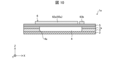
- FIG. 10 is a cross-sectional view of the elastic wave device 1a according to the second embodiment.
- the elastic wave device 1a differs from the elastic wave device 1 in that a connection layer 7a of silicon dioxide (SiO 2 ) is provided between the silicon 3 and the piezoelectric substrate 5.
- the connection layer 7a exists only above the silicon 3 and does not exist at the position of the cavity 4.
- the connection layer 7a has a thickness of about 0.1 ⁇ m.
- FIG. 13 is a cross-sectional view of an elastic wave device 1b according to the third embodiment.
- the elastic wave device 1b differs from the elastic wave device 1 in that a low resistance connection layer 7b is provided between the silicon 3 and the piezoelectric substrate 5.
- the connection layer 7b exists only above the silicon 3 and does not exist at the position of the cavity 4.
- the transverse mode index T is sufficiently small compared to Comparative Example 1 until the position of the outer edge 4a is located at the end of the low sound velocity region 66.
- the phase average value is also sufficiently close to 90° until the position of the outer edge 4a is located at the end of the low sound velocity region 66. Therefore, in the elastic wave device 1c according to the fourth embodiment, it can be said that the frequency characteristics are sufficiently good until the position of the outer edge 4a is located at the end of the low sound velocity region 66.
- the transverse mode index T is sufficiently small compared to Comparative Example 1 until the position of the outer edge 4a is located at the end of the low sound velocity region 66.
- the phase average value is also sufficiently close to 90° until the position of the outer edge 4a is located at the end of the low sound velocity region 66. Therefore, in the elastic wave device according to the fifth embodiment, it can be said that the frequency characteristics are sufficiently good until the position of the outer edge 4a is located at the end of the low sound velocity region 66.
- Embodiments 1 and 5 are the same except for the value of the offset duty OD, and good frequency characteristics could be obtained even if the offset duty OD was increased.
- the offset duty OD of the IDT electrode 6 is increased to 0.8 compared to the elastic wave device 1. In other words, the weight of the low sound velocity region 66 is increased.
- FIG. 21 is a graph showing the transverse mode index T according to the silicon penetration amount x in the elastic wave device according to the sixth embodiment.
- FIG. 22 shows the phase average value from the resonant frequency fr to the anti-resonant frequency fa according to the amount x of silicon penetration in the elastic wave device according to the sixth embodiment.
- the broken lines in FIGS. 21 and 22 are the values in Comparative Example 1, and the solid lines are the values in the elastic wave device according to the fifth embodiment.
- FIG. 23 is a graph showing the transverse mode index T according to the width of the bus bar in the elastic wave device 1 according to the seventh embodiment.
- FIG. 24 shows phase average values from the resonant frequency fr to the anti-resonant frequency fa according to the width of the bus bar in the elastic wave device 1 according to the seventh embodiment.
- the silicon penetration amount x was assumed to be located below the tip of the dummy electrode finger 63.
- FIG. 25 is a plan view of the elastic wave device according to the eighth embodiment.
- the elastic wave device includes an IDT electrode 6f that is a piston resonator instead of the IDT electrode 6.
- the root of the electrode finger 62 in contact with the bus bar 61 and the tip of the electrode finger 62 are widened, and are a widened part 65 and a widened part 67, respectively. Further, the piston resonator does not include dummy electrode fingers 63. Furthermore, the bus bar 61 is provided with an opening 68 . The widened portion 67 and the opening 68 are classified into a widened portion 67a and a widened portion 67b, and an opening 68a and an opening 68b, depending on the applied potential.
- FIG. 28 is a diagram illustrating a schematic configuration of the communication device 151 in the ninth embodiment.
- the communication device 151 is an application example of an elastic wave device according to one aspect of the present disclosure, and performs wireless communication using radio waves.
- the communication device 151 may include one duplexer 101 as a transmission filter 109 and another duplexer 101 as a reception filter 111.
- Each of the two duplexers 101 may include an elastic wave device (eg, elastic wave device 1, 1a to 1f) according to one aspect of the present disclosure. In this way, the communication device 151 may include an elastic wave device according to one aspect of the present disclosure.
- a transmission information signal TIS containing information to be transmitted is modulated and frequency-increased (converted to a high-frequency signal having a carrier frequency) by an RF-IC (Radio Frequency-Integrated Circuit) 153, and the transmission information signal TIS is converted into a transmission signal. It may be converted to TS.
- the bandpass filter 155 may remove unnecessary components other than the transmission passband for the TS.
- the TS after removing unnecessary components may be amplified by the amplifier 157 and input to the transmission filter 109.
- the transmission filter 109 may remove unnecessary components outside the transmission passband from the input transmission signal TS.
- the transmission filter 109 may output the TS from which unnecessary components have been removed to the antenna 159 via an antenna terminal (eg, TCin described above).
- the antenna 159 may convert the TS, which is an electrical signal input to itself, into a radio wave as a wireless signal, and transmit the radio wave to the outside of the communication device 151.
- the antenna 159 may convert the received radio waves from the outside into a reception signal RS, which is an electrical signal, and input the RS to the reception filter 111 via the antenna terminal.
- the reception filter 111 may remove unnecessary components other than the reception passband from the input RS.
- the reception filter 111 may output the reception signal RS from which unnecessary components have been removed to the amplifier 161.
- the output RS may be amplified by the amplifier 161.
- the bandpass filter 163 may remove unnecessary components other than the receiving passband from the amplified RS.
- the frequency of the RS after unnecessary component removal is lowered and demodulated by the RF-IC 153, and may be converted into a received information signal RIS.
- the TIS and RIS may be low frequency signals (baseband signals) containing appropriate information.
- TIS and RIS may be analog audio signals or digitized audio signals.
- the passband of the wireless signal may be set as appropriate and may conform to various known standards.
- the low sound velocity region 66 was defined by the length of the widened portion 65 in the extending direction of the electrode fingers, but this is not the case. Specifically, the low sound velocity region 66 may be defined by adding an additional film to the electrode finger 62 instead of the widened portion 65 to increase the weight of at least a portion of the electrode finger 62. good. That is, the frequency characteristics of the elastic wave device may be improved by creating a low sound velocity region 66 in which the weight per unit length of the electrode finger is increased.
- An elastic wave device includes: a support substrate in which a cavity is formed; a piezoelectric substrate located on the support substrate and covering the cavity; and a piezoelectric substrate located on the piezoelectric substrate.
- an IDT electrode the IDT electrode has a pair of bus bars and a plurality of electrode fingers provided in a first region sandwiched between the pair of bus bars, and an intersection region in the first region. is arranged so as to overlap the hollow portion in plan view, and the first region has a higher elasticity in the arrangement direction of the plurality of electrode fingers than at least some other regions in the first region.
- the area includes a low sound speed area extending in the arrangement direction, where the sound speed of waves is low, and the outer edge of the cavity portion and the low sound speed area overlap in plan view.
- the low sound velocity region may be configured by providing a widened portion in the plurality of electrode fingers.
- the electrode finger may have a low sound velocity region, and the low sound velocity region is widened.
- the low sound velocity region may be configured by providing an additional film on the plurality of electrode fingers.
- the electrode finger may have a low sound velocity region, and the low sound velocity region has an additional film.
- the low sound velocity region faces the electrode fingers in the extending direction of the electrode fingers, and has an average width of the electrode fingers.
- the second electrode finger may be provided with a width larger than that of the second electrode finger.
- the second electrode finger may be provided as the low sound velocity region.
- the low sound velocity region may be a part of the region near the pair of bus bars.
- the low sound velocity region can be located near the bus bar.
- the widened portion may be provided on the tip side of the electrode finger.
- the low sound velocity region can be located on the tip side of the electrode finger.
- the distance from the low sound velocity region to the intersection region may be within one wavelength.
- the distance from the low sound velocity region to the crossing region is within the attachment pitch of the plurality of electrode fingers. Good too.
- the low sound velocity region can exist up to the vicinity of the intersection region.
- the bus bar may be configured by providing a gap.
- the support substrate may be made of silicon.
- silicon can be used as the support substrate.
- the IDT electrode may excite an elastic wave of an A1 moderam wave.
- the IDT electrode can excite the elastic wave of the A1 moderam wave.
- the elastic wave device according to aspect 12 of the present disclosure may be a communication device including the elastic wave device in any one of aspects 1 to 11.
- the communication device can be filtered by the elastic wave device.
Landscapes
- Physics & Mathematics (AREA)
- Acoustics & Sound (AREA)
- Surface Acoustic Wave Elements And Circuit Networks Thereof (AREA)
Abstract
スプリアスを低減する。空洞部が形成された、支持基板と、指示基板の上に位置し、空洞部を覆う、圧電基板と、圧電基板の上に位置する、IDT電極と、を備え、IDT電極は、バスバーと、複数の電極指と、バスバーに挟まれた第1領域と、を有し、空洞部と、複数の電極指が交差する交差領域の全体と、が平面透視で重なり、第1領域は、電極指の配列方向に延在する、低音速領域を有し、空洞部の外縁と、低音速領域とが平面透視で重なる。
Description
本開示は弾性波装置に関する。
下記の特許文献1には、メンブレン構造を備えた弾性波装置の一構成例が開示されている。
上記の課題を解決するために、本開示の一態様に係る弾性波装置は、空洞部が形成された、支持基板と、前記指示基板の上に位置し、前記空洞部を覆う、圧電基板と、前記圧電基板の上に位置する、IDT電極と、を備え、前記IDT電極は、バスバーと、複数の電極指と、前記バスバーに挟まれた第1領域と、を有し、前記空洞部と、前記複数の電極指が交差する交差領域の全体と、が平面透視で重なり、前記第1領域は、前記電極指の配列方向に延在する、低音速領域を有し、前記空洞部の外縁と、前記低音速領域とが平面透視で重なる。
メンブレン構造を備えた弾性波装置において、スプリアスを低減したフィルタ特性を実現することが望まれる。
〔実施形態1〕
実施形態1に係る弾性波装置について、以下に説明する。説明の便宜上、実施形態1にて説明したコンポーネント(構成要素)と同じ機能を有するコンポーネントについては、以降の各実施形態では同じ符号を付し、その説明を繰り返さない。簡潔化のため、公知の技術事項についても説明を適宜省略する。本明細書において述べる各コンポーネント、各材料、および各数値は、特に矛盾のない限り、いずれも単なる一例である。それゆえ、例えば、特に矛盾のない限り、各コンポーネントの位置関係は、各図の例に限定されない。また、各コンポーネントの図示は、必ずしもスケール通りではない。
実施形態1に係る弾性波装置について、以下に説明する。説明の便宜上、実施形態1にて説明したコンポーネント(構成要素)と同じ機能を有するコンポーネントについては、以降の各実施形態では同じ符号を付し、その説明を繰り返さない。簡潔化のため、公知の技術事項についても説明を適宜省略する。本明細書において述べる各コンポーネント、各材料、および各数値は、特に矛盾のない限り、いずれも単なる一例である。それゆえ、例えば、特に矛盾のない限り、各コンポーネントの位置関係は、各図の例に限定されない。また、各コンポーネントの図示は、必ずしもスケール通りではない。
(比較例:一般的なIDT電極600の構造)
実施形態1の説明に先立ち、一般的な弾性波装置に関して説明する。図29は、一般的な弾性波装置100におけるIDT電極600の1周期分を平面視した図である。そのため、IDT電極600は、電極指の配列方向(Y方向)に配列されている。図30は、一般的な弾性波装置100の断面図である。
実施形態1の説明に先立ち、一般的な弾性波装置に関して説明する。図29は、一般的な弾性波装置100におけるIDT電極600の1周期分を平面視した図である。そのため、IDT電極600は、電極指の配列方向(Y方向)に配列されている。図30は、一般的な弾性波装置100の断面図である。
弾性波装置100は、種々の材料からなる支持部2の上に、シリコン3が部分的に形成されている。支持部2の材料は、例えばシリコンであってもよいし、その他の材料であってもよい。支持部2がシリコンである場合、シリコン3と貼り合わせられてもよいし、一体で形成されてもよい。支持部2が存在せず、シリコン3によって支持されてもよい。支持部2に対して、シリコン3が形成されていない領域は空洞部4である。支持部2は、平面視で空洞部4と重なる領域において、開口を有していてもよい。支持部2およびシリコン3を合わせて支持基板と称してもよい。弾性波装置100は、シリコン3および空洞部4の上部にさらに圧電基板5が形成されており、圧電基板5は空洞部4を覆う。圧電基板5は、105°Y‐XLiNb3などで形成する。105°Y‐XLiNb3は、105°回転YカットX伝播LiNb3とも呼ぶ。
弾性波装置100は、圧電基板5のさらに上部のうち空洞部4に対応する領域に、IDT電極600が形成されている。IDT電極600は、それぞれ異なる電位が印加される、バスバー61aおよびバスバー61bと、電極指62aおよび電極指62bと、ダミー電極指63aおよびダミー電極指63b(ともに、第2電極指)と、を備える。以降、それぞれの電位を考慮しない場合は、バスバー61、電極指62、およびダミー電極指63と記す。IDT電極600によって、圧電基板5にA1モードラム波の弾性波が励振される。
なお、IDT電極600によって、圧電基板5にバルク波の弾性波が励振されてもよい。厚み滑りモードのバルク波が励振されてもよい。
IDT電極600では、バスバー61に電極指62およびダミー電極指63が交互に接続されている。電極指62はX方向に長い電極であり、ダミー電極指63はX方向に短い電極である。電極指62aおよびダミー電極指63bは対向し、電極指62bおよびダミー電極指63aは対向する。バスバー61に挟まれた領域を、第1領域60と称する。そのため、電極指62およびダミー電極指63は第1領域60に存在する。
電極指62aと電極指62bとが交差している領域が交差領域64である。例えば、電極指62aと電極指62bとに対し、交流印加されたIDT電極600によって、交差領域64における圧電基板5に板波が励振される。
交差領域64における、電極指62aの電極指の配列方向上端から、電極指62bの電極指の配列方向上端までの、距離をピッチPTと称し、ピッチPTに対する電極指62の幅の比率をデューティDと称する。
(比較例1:一般的なIDT電極600の周波数特性)
図31は、比較例1に係る一般的な弾性波装置100での周波数特性を表す図である。図31では、横軸に周波数を、縦軸に位相をとっている。弾性波装置100では、位相が90°で一定であってもよい。
図31は、比較例1に係る一般的な弾性波装置100での周波数特性を表す図である。図31では、横軸に周波数を、縦軸に位相をとっている。弾性波装置100では、位相が90°で一定であってもよい。
図31に示すように、例えば約5590MHz、約5655MHz近傍において、位相が急激に低下している。このように、周波数に対する位相の所望でない急変化があることをスプリアスと称することがある。弾性波装置100ではスプリアスが発生している。以降は、この図31を比較対象として、本開示の構成に基づく弾性波装置の優位性を示していく。
(比較例2:IDT電極600の下方にシリコン3が侵入した場合での周波数特性)
比較例2に係る弾性波装置は、弾性波装置100に対して、空洞部4が小さく、シリコン3がIDT電極600の下方に侵入している。すなわち、空洞部4の外縁4aがIDT電極600の下方に位置する。比較例2に係る弾性波装置は、電極指のデューティが、根本から先端まで一定である。ダミー電極指も、電極指と同じデューティを有する。このような弾性波装置を、非デューティオフセット共振子または通常共振子とも呼称する。
比較例2に係る弾性波装置は、弾性波装置100に対して、空洞部4が小さく、シリコン3がIDT電極600の下方に侵入している。すなわち、空洞部4の外縁4aがIDT電極600の下方に位置する。比較例2に係る弾性波装置は、電極指のデューティが、根本から先端まで一定である。ダミー電極指も、電極指と同じデューティを有する。このような弾性波装置を、非デューティオフセット共振子または通常共振子とも呼称する。
図32は、比較例2に係る弾性波装置での周波数特性を表す図である。図32の上図のグラフでは、横軸に周波数を、縦軸に位相をとっている。実線は比較例2に係る弾性波装置において、シリコン3がIDT電極600の下方に侵入している場合の周波数特性であり、破線は比較例2に係る弾性波装置において、シリコン3がIDT電極600の下方に侵入していない場合の周波数特性である。図32の下部の模式図は、シリコン3の侵入量を表す模式図である。実線の場合における、シリコン3の侵入量は、0.5μmである。0.5μmは、バスバーの太さの1/3に相当する。
図32に示すように、比較例2に係る周波数特性は、比較例1に係る周波数特性と大差なく、スプリアスが生じていることがわかる。
(IDT電極6の構成)
次に、実施形態1に係るIDT電極の形状を説明した後に、当該IDT電極によってスプリアスが低減できたことを示す。
次に、実施形態1に係るIDT電極の形状を説明した後に、当該IDT電極によってスプリアスが低減できたことを示す。
図1は、実施形態1に係る弾性波装置1の一部を平面視した図である。弾性波装置1は、IDT電極600に代えて、IDT電極6が形成されている点が、弾性波装置100と異なっている。
IDT電極6は、それぞれ異なる電位が印加される、バスバー61aおよびバスバー61bと、電極指62aおよび電極指62bと、ダミー電極指63aおよびダミー電極指63bと、拡幅部65aおよび65b(拡幅部65とも称する)と、を備える。拡幅部65は第1領域60におけるバスバー61の近傍に位置する。
また、バスバー61の近傍に位置する拡幅部65は、交差領域64のバスバー側の端から1波長以内の範囲か、または、ピッチPTの範囲に存在してもよい。
IDT電極6では、バスバー61に拡幅部65およびダミー電極指63が交互に接続されており、拡幅部65に電極指62が接続されている。電極指62とダミー電極指63とが対向することは変わりない。
拡幅部65のピッチPTに対する幅の比率をオフセットデューティODと称し、オフセットデューティODは、デューティDよりも大きい。つまり、拡幅部65のY方向(電極指の配列方向)の幅は、電極指62のY方向の幅よりも大きい(拡幅している)。また、拡幅部65のX方向(電極指の延伸方向)の長さは、ダミー電極指63の長さよりも長い。このような拡幅部65を有するIDT電極6のことをデューティオフセット共振子と称する。また、ダミー電極指(第2電極指)63は、電極指62の平均幅よりも大きい幅を有する。
拡幅部65の幅における電極指62の配列方向に延在する領域を低音速領域66と称する。電極指62のデューティDよりも、拡幅部65のオフセットデューティODが大きいため、拡幅部65の方が電極指62よりも単位面積当たりの重量が大きい。そのため、低音速領域66の音速は、第1領域60の中では低くなる。
(IDT電極6の断面形状ごとの周波数特性)
比較例では、IDT電極600が空洞部4に対応する領域の上方に配置されたが、IDT電極6はこの限りではない。具体的には、実施形態1に係る弾性波装置1では、シリコン3がIDT電極6の下方まで存在し、外縁4aがIDT電極6の下方に位置する。以下に説明するように弾性波装置1では、空洞部4の外縁4aと、低音速領域66とが平面透視で重なる。
比較例では、IDT電極600が空洞部4に対応する領域の上方に配置されたが、IDT電極6はこの限りではない。具体的には、実施形態1に係る弾性波装置1では、シリコン3がIDT電極6の下方まで存在し、外縁4aがIDT電極6の下方に位置する。以下に説明するように弾性波装置1では、空洞部4の外縁4aと、低音速領域66とが平面透視で重なる。
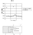
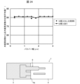
図2は、実施形態1に係る弾性波装置1の断面図である。図2では、図30と異なり、シリコン3がIDT電極6の下方に侵入している。この侵入量をシリコン侵入量xとし、xは、第1領域60外におけるバスバー61の端部からの空洞部4の外縁4aまでの距離である。シリコン侵入量xは変数であり、以降シリコン侵入量xを調整しながら弾性波装置の周波数特性をシミュレーションした。IDT電極6では、デューティDを0.5、オフセットデューティODを0.6とした。
図3は、外縁4aの位置がバスバー61の端部と一致する場合の周波数特性である。図4は、外縁4aの位置がバスバー61の内部の下方に位置する場合の周波数特性である。図5は、外縁4aの位置がダミー電極指63の内部の下方に位置する場合の周波数特性である。図6は、外縁4aの位置が交差領域64の端部に位置する場合の周波数特性である。図7は、外縁4aの位置が、拡幅部65の端部に位置する場合の周波数特性である。
図3~図7の上部のグラフにおいて、破線は、比較例1の場合の周波数特性を表し、実線がそれぞれの場合を表す。図3~図7の下部の模式図は、シリコン3の侵入量を表す模式図である。図3~図7に示すように、シリコン3のIDT電極6の下方へのシリコン侵入量xに応じて、周波数特性は変化している。
図3~7に示すように、外縁4aの位置が、バスバー61の端部と一致する場合から低音速領域の端部に位置する場合までは、スプリアスが低減できていることがわかる。
(横モード指標の導入)
シリコン3のIDT電極6の下方へのシリコン侵入量xに応じた、周波数特性を定量化するために、横モード指標Tを導入する。横モード指標Tは次式で表せる。

ここで、Pは位相であり、fは周波数である。Δfは、反共振周波数faと、共振周波数frとの差である。
シリコン3のIDT電極6の下方へのシリコン侵入量xに応じた、周波数特性を定量化するために、横モード指標Tを導入する。横モード指標Tは次式で表せる。
dP/dfは位相の傾きであるため、横モード指標Tは通過帯域内の単位周波数あたりの傾きの絶対値になる。そのため、横モード指標Tが大きいほど、通過帯域内において位相特性がフラットではなく、スプリアスが顕著に存在していることを表している。横モード指標Tが小さい領域を、発明者は探索した。
(周波数特性)
図8は、実施形態1に係る弾性波装置1におけるシリコン侵入量xに応じた横モード指標Tを表すグラフである。図9は、実施形態1に係る弾性波装置1におけるシリコン侵入量xに応じた共振周波数frから反共振周波数faの位相平均値である。図8および図9における破線は比較例における値であり、実線は実施形態1に係る弾性波装置1における値である。図8および図9は、図3~図7における周波数特性を指標毎に一つのグラフに集約したものである。
図8は、実施形態1に係る弾性波装置1におけるシリコン侵入量xに応じた横モード指標Tを表すグラフである。図9は、実施形態1に係る弾性波装置1におけるシリコン侵入量xに応じた共振周波数frから反共振周波数faの位相平均値である。図8および図9における破線は比較例における値であり、実線は実施形態1に係る弾性波装置1における値である。図8および図9は、図3~図7における周波数特性を指標毎に一つのグラフに集約したものである。
図8に示すように、外縁4aの位置が、低音速領域66の端部に位置するまで、横モード指標Tは比較例に対して十分小さいことがわかる。また、図9に示すように、外縁4aの位置が、低音速領域66の端部に位置するまで、位相平均値も十分に90°に近いことがわかる。したがって、実施形態1に係る弾性波装置1では、外縁4aの位置が、低音速領域66の端部に位置するまでは、周波数特性は十分に良好といえる。
(小括)
実施形態1に係る弾性波装置1のような、低音速領域66を有するデューティオフセット共振子に対し、シリコン3がデューティオフセット共振子の下まで入り込むことによって、周波数特性が変化することを調査した。具体的には、外縁4aが、第1領域60外におけるバスバー61の端部から、第1領域60の範囲に位置する場合を調査した。
実施形態1に係る弾性波装置1のような、低音速領域66を有するデューティオフセット共振子に対し、シリコン3がデューティオフセット共振子の下まで入り込むことによって、周波数特性が変化することを調査した。具体的には、外縁4aが、第1領域60外におけるバスバー61の端部から、第1領域60の範囲に位置する場合を調査した。
その結果、デューティオフセット共振子では、外縁4a(空洞部4に対するエッジ)の位置が、低音速領域66のバスバー61の端部から、低音速領域66の端部の位置までにある場合、周波数特性は十分に良好であることがわかった。また、図3~図7によって、スプリアスを低減することができることがわかった。
〔実施形態2〕
図10は、実施形態2に係る弾性波装置1aの断面図である。弾性波装置1aは、弾性波装置1に対して、シリコン3と圧電基板5の間に、二酸化ケイ素(SiO2)の接続層7aを備える点が異なる。接続層7aは、シリコン3のみの上部に存在し、空洞部4の位置には存在しない。接続層7aは0.1μmほどの厚さである。
図10は、実施形態2に係る弾性波装置1aの断面図である。弾性波装置1aは、弾性波装置1に対して、シリコン3と圧電基板5の間に、二酸化ケイ素(SiO2)の接続層7aを備える点が異なる。接続層7aは、シリコン3のみの上部に存在し、空洞部4の位置には存在しない。接続層7aは0.1μmほどの厚さである。
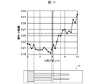
図11は、実施形態2に係る弾性波装置1aにおけるシリコン侵入量xに応じた横モード指標Tを表すグラフである。図12は、実施形態2に係る弾性波装置1aにおけるシリコン侵入量xに応じた共振周波数frから反共振周波数faの位相平均値である。図11および図12における破線は比較例1における値であり、実線は実施形態2に係る弾性波装置1aにおける値である。
図11に示すように、外縁4aの位置が、低音速領域66の端部に位置するまで、横モード指標Tは比較例1に対して十分小さいことがわかる。また、図12に示すように、外縁4aの位置が、低音速領域66の端部に位置するまで、位相平均値も十分に90°に近いことがわかる。したがって、実施形態2に係る弾性波装置1aでは、外縁4aの位置が、低音速領域66の端部に位置するまでは、周波数特性は十分に良好といえる。
〔実施形態3〕
図13は、実施形態3に係る弾性波装置1bの断面図である。弾性波装置1bは、弾性波装置1に対して、シリコン3と圧電基板5との間に、低抵抗層の接続層7bを備える点が異なる。接続層7bは、シリコン3のみの上部に存在し、空洞部4の位置には存在しない。
図13は、実施形態3に係る弾性波装置1bの断面図である。弾性波装置1bは、弾性波装置1に対して、シリコン3と圧電基板5との間に、低抵抗層の接続層7bを備える点が異なる。接続層7bは、シリコン3のみの上部に存在し、空洞部4の位置には存在しない。
低抵抗層は、接合する界面で特性を悪くする界面である。低抵抗層は、リチウム、ニオブ、ケイ素、および酸素などの化合物である。低抵抗層の厚さは2nmほどであり、5500MHzほどの周波数において、例えば2.5Ω・cm程度の抵抗率を有する。
図14は、実施形態3に係る弾性波装置1bにおけるシリコン侵入量xに応じた横モード指標Tを表すグラフである。図15は、実施形態3に係る弾性波装置1bにおけるシリコン侵入量xに応じた共振周波数frから反共振周波数faの位相平均値である。図14および図15における破線は比較例1における値であり、実線は実施形態3に係る弾性波装置1bにおける値である。
図14に示すように、外縁4aの位置が、低音速領域66の端部に位置するまで、横モード指標Tは比較例1に対して十分小さいことがわかる。また、図15に示すように、外縁4aの位置が、低音速領域66の端部に位置するまで、位相平均値も十分に90°に近いことがわかる。したがって、実施形態3に係る弾性波装置1bでは、外縁4aの位置が、低音速領域66の端部に位置するまでは、周波数特性は十分に良好といえる。
〔実施形態4〕
図16は、実施形態4に係る弾性波装置1cの断面図である。弾性波装置1cは、弾性波装置1に対して、シリコン3と圧電基板5の間に、窒化アルミ(AlN)の接続層7cを備える点が異なる。接続層7cは、シリコン3のみの上部に存在し、空洞部4の位置には存在しない。接続層7cは0.1μmほどの厚さである。
図16は、実施形態4に係る弾性波装置1cの断面図である。弾性波装置1cは、弾性波装置1に対して、シリコン3と圧電基板5の間に、窒化アルミ(AlN)の接続層7cを備える点が異なる。接続層7cは、シリコン3のみの上部に存在し、空洞部4の位置には存在しない。接続層7cは0.1μmほどの厚さである。
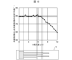
図17は、実施形態4に係る弾性波装置1cにおけるシリコン侵入量xに応じた横モード指標Tを表すグラフである。図18は、実施形態4に係る弾性波装置1cにおけるシリコン侵入量xに応じた共振周波数frから反共振周波数faの位相平均値である。図17および図18における破線は比較例1における値であり、実線は実施形態4に係る弾性波装置1cにおける値である。
図17に示すように、外縁4aの位置が、低音速領域66の端部に位置するまで、横モード指標Tは比較例1に対して十分小さいことがわかる。また、図18に示すように、外縁4aの位置が、低音速領域66の端部に位置するまで、位相平均値も十分に90°に近いことがわかる。したがって、実施形態4に係る弾性波装置1cでは、外縁4aの位置が、低音速領域66の端部に位置するまでは、周波数特性は十分に良好といえる。
〔実施形態5〕
実施形態5に係る弾性波装置1dは、弾性波装置1に対して、IDT電極6のオフセットデューティODが0.7に増加している。つまり、低音速領域66の重量が増加している。
実施形態5に係る弾性波装置1dは、弾性波装置1に対して、IDT電極6のオフセットデューティODが0.7に増加している。つまり、低音速領域66の重量が増加している。
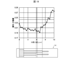
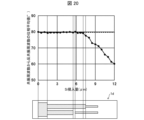
図19は、実施形態5に係る弾性波装置におけるシリコン侵入量xに応じた横モード指標Tを表すグラフである。図20は、実施形態5に係る弾性波装置におけるシリコン侵入量xに応じた共振周波数frから反共振周波数faの位相平均値である。図19および図20における破線は比較例1における値であり、実線は実施形態5に係る弾性波装置における値である。
図19に示すように、外縁4aの位置が、低音速領域66の端部に位置するまで、横モード指標Tは比較例1に対して十分小さいことがわかる。また、図20に示すように、外縁4aの位置が、低音速領域66の端部に位置するまで、位相平均値も十分に90°に近いことがわかる。したがって、実施形態5に係る弾性波装置では、外縁4aの位置が、低音速領域66の端部に位置するまでは、周波数特性は十分に良好といえる。
実施形態1および実施形態5では、オフセットデューティODの値が異なるだけで他は同じであり、オフセットデューティODを大きくしても良好な周波数特性を得ることができた。
〔実施形態6〕
実施形態6に係る弾性波装置1eは、弾性波装置1に対して、IDT電極6のオフセットデューティODが0.8に増加している。つまり、低音速領域66の重量が増加している。
実施形態6に係る弾性波装置1eは、弾性波装置1に対して、IDT電極6のオフセットデューティODが0.8に増加している。つまり、低音速領域66の重量が増加している。
図21は、実施形態6に係る弾性波装置におけるシリコン侵入量xに応じた横モード指標Tを表すグラフである。図22は、実施形態6に係る弾性波装置におけるシリコン侵入量xに応じた共振周波数frから反共振周波数faの位相平均値である。図21および図22における破線は比較例1における値であり、実線は実施形態5に係る弾性波装置における値である。
図21に示すように、外縁4aの位置が、低音速領域66の端部に位置するまで、横モード指標Tは比較例1に対して十分小さいことがわかる。また、図22に示すように、外縁4aの位置が、低音速領域66の端部に位置するまで、位相平均値も十分に90°に近いことがわかる。したがって、実施形態5に係る弾性波装置では、外縁4aの位置が、低音速領域66の端部に位置するまでは、周波数特性は十分に良好といえる。
実施形態1および実施形態6では、オフセットデューティODの値が異なるだけで他は同じであり、オフセットデューティODを大きくしても良好な周波数特性を得ることができた。
〔実施形態7〕
実施形態7に係る弾性波装置1は、IDT電極6のバスバー61の幅が異なる。図23は、実施形態7に係る弾性波装置1におけるバスバーの幅に応じた横モード指標Tを表すグラフである。図24は、実施形態7に係る弾性波装置1におけるバスバーの幅に応じた共振周波数frから反共振周波数faの位相平均値である。シリコン侵入量xは、ダミー電極指63の先端の下方に位置する場合とした。
実施形態7に係る弾性波装置1は、IDT電極6のバスバー61の幅が異なる。図23は、実施形態7に係る弾性波装置1におけるバスバーの幅に応じた横モード指標Tを表すグラフである。図24は、実施形態7に係る弾性波装置1におけるバスバーの幅に応じた共振周波数frから反共振周波数faの位相平均値である。シリコン侵入量xは、ダミー電極指63の先端の下方に位置する場合とした。
図23および図24に示すように、バスバー61の幅を変更することに伴う、横モード指標Tおよび位相平均値に対する影響がないことが確認された。
〔実施形態8〕
図25は、実施形態8に係る弾性波装置を平面視した図である。弾性波装置は、IDT電極6に代えて、ピストン共振子であるIDT電極6fを備える。
図25は、実施形態8に係る弾性波装置を平面視した図である。弾性波装置は、IDT電極6に代えて、ピストン共振子であるIDT電極6fを備える。
ピストン共振子は、電極指62において、バスバー61に接する根本と、電極指62の先端とが、拡幅しているものであり、それぞれ、拡幅部65および拡幅部67である。また、ピストン共振子では、ダミー電極指63を備えない。さらに、バスバー61において、開口部68を備える。拡幅部67および開口部68は、印加される電位に応じて、拡幅部67aおよび拡幅部67bと、開口部68aおよび開口部68bと、に分類される。
図26は、実施形態8に係る弾性波装置におけるシリコン侵入量xに応じた横モード指標Tを表すグラフである。図27は、実施形態8に係る弾性波装置におけるシリコン侵入量xに応じた共振周波数frから反共振周波数faの位相平均値である。図26および図27における破線は比較例における値であり、実線は実施形態8に係る弾性波装置における値である。
図26に示すように、外縁4aの位置が、低音速領域66の端部に位置するまで、横モード指標Tは比較例1に対して十分小さいことがわかる。また、図27に示すように、外縁4aの位置が、低音速領域66の端部に位置するまで、位相平均値も十分に90°に近いことがわかる。したがって、実施形態8に係る弾性波装置では、外縁4aの位置が、低音速領域66の端部に位置するまでは、周波数特性は十分に良好といえる。
〔実施形態9〕
図28は、実施形態9における通信装置151の概略的な構成を例示する図である。通信装置151は、本開示の一態様に係る弾性波装置の一適用例であり、電波を利用した無線通信を行う。通信装置151は、送信フィルタ109としての1つの分波器101と、受信フィルタ111としての別の1つの分波器101とを含んでいてよい。2つの分波器101のそれぞれは、本開示の一態様に係る弾性波装置(例:弾性波装置1、1a~1f)を含んでいてよい。このように、通信装置151は、本開示の一態様に係る弾性波装置を含んでいてよい。
図28は、実施形態9における通信装置151の概略的な構成を例示する図である。通信装置151は、本開示の一態様に係る弾性波装置の一適用例であり、電波を利用した無線通信を行う。通信装置151は、送信フィルタ109としての1つの分波器101と、受信フィルタ111としての別の1つの分波器101とを含んでいてよい。2つの分波器101のそれぞれは、本開示の一態様に係る弾性波装置(例:弾性波装置1、1a~1f)を含んでいてよい。このように、通信装置151は、本開示の一態様に係る弾性波装置を含んでいてよい。
通信装置151において、送信すべき情報を含む送信情報信号TISは、RF-IC(Radio Frequency-Integrated Circuit)153によって変調および周波数の引き上げ(搬送波周波数を有する高周波信号への変換)がなされ、送信信号TSへと変換されてよい。バンドパスフィルタ155は、TSについて、送信用の通過帯以外の不要成分を除去してよい。次いで、不要成分除去後のTSは、増幅器157によって増幅されて、送信フィルタ109に入力されてよい。
送信フィルタ109は、入力された送信信号TSから送信用の通過帯以外の不要成分を除去してよい。送信フィルタ109は、アンテナ端子(例:上述のTCin)を介して、不要成分除去後のTSをアンテナ159に出力してよい。アンテナ159は、自身に入力された電気信号であるTSを、無線信号としての電波に変換し、当該電波を通信装置151の外部に送信してよい。
また、アンテナ159は、受信した外部からの電波を、電気信号である受信信号RSに変換し、アンテナ端子を介して当該RSを受信フィルタ111に入力してよい。受信フィルタ111は、入力されたRSから受信用の通過帯以外の不要成分を除去してよい。受信フィルタ111は、不要成分除去後の受信信号RSを増幅器161へ出力してよい。出力されたRSは、増幅器161によって増幅されてよい。バンドパスフィルタ163は、増幅後のRSについて、受信用の通過帯以外の不要成分を除去してよい。不要成分除去後のRSは、RF-IC153によって周波数の引き下げおよび復調がなされ、受信情報信号RISへと変換されてよい。
TISおよびRISは、適宜な情報を含む低周波信号(ベースバンド信号)であってよい。例えば、TISおよびRISは、アナログ音声信号であってもよいし、あるいはデジタル化された音声信号であってよい。無線信号の通過帯は、適宜に設定されてよく、公知の各種の規格に準拠してよい。
実施形態1から8では、低音速領域66は、拡幅部65の電極指の延伸方向の長さによって画定されたが、この限りではない。具体的には、拡幅部65に代えて、電極指62上に、付加膜を付加することによって、電極指62の少なくとも一部の重量を増加させることで、低音速領域66を画定してもよい。すなわち、電極指の単位長さ辺りの重量を増やした低音速領域66を作ることによって、弾性波装置の周波数特性を改善すればよい。
〔まとめ〕
本開示の態様1に係る弾性波装置は、空洞部が形成された、支持基板と、前記支持基板の上に位置し、前記空洞部を覆う、圧電基板と、前記圧電基板の上に位置する、IDT電極と、を備え、前記IDT電極は、一対のバスバーと、前記一対のバスバーに挟まれた第1領域に設けられた複数の電極指と、を有し、前記第1領域における交差領域の全体は、前記空洞部と平面透視で重なるように配置されており、前記第1領域は、前記第1領域における他の少なくとも一部の領域よりも、前記複数の電極指の配列方向の弾性波の音速が小さい領域であって、当該配列方向に延在する、低音速領域を含み、前記空洞部の外縁と、前記低音速領域とが平面透視で重なる。
本開示の態様1に係る弾性波装置は、空洞部が形成された、支持基板と、前記支持基板の上に位置し、前記空洞部を覆う、圧電基板と、前記圧電基板の上に位置する、IDT電極と、を備え、前記IDT電極は、一対のバスバーと、前記一対のバスバーに挟まれた第1領域に設けられた複数の電極指と、を有し、前記第1領域における交差領域の全体は、前記空洞部と平面透視で重なるように配置されており、前記第1領域は、前記第1領域における他の少なくとも一部の領域よりも、前記複数の電極指の配列方向の弾性波の音速が小さい領域であって、当該配列方向に延在する、低音速領域を含み、前記空洞部の外縁と、前記低音速領域とが平面透視で重なる。
上記の構成によれば、スプリアスを低減し、周波数特性を改善することができる。
本開示の態様2に係る弾性波装置は、前記態様1において、前記低音速領域は、前記複数の電極指に拡幅部が設けられることによって構成されてもよい。
上記の構成によれば、電極指は、低音速領域を有してもよく、低音速領域は、拡幅している。
本開示の態様3に係る弾性波装置は、前記態様1または2において、前記低音速領域は、前記複数の電極指に付加膜が設けられることによって構成されてもよい。
上記の構成によれば、電極指は、低音速領域を有してもよく、低音速領域は、付加膜を有している。
本開示の態様4に係る弾性波装置は、前記態様1から3のいずれか1つにおいて、前記低音速領域は、前記電極指の延伸方向において前記電極指に対向し、前記電極指の平均幅よりも大きい幅を有する第2電極指が設けられることによって構成されてもよい。
上記の構成によれば、低音速領域として、第2電極指を有してもよい。
本開示の態様5に係る弾性波装置は、前記態様1から4のいずれか1つにおいて、前記低音速領域は、前記一対のバスバーの近傍の一部の領域であってもよい。
上記の構成によれば、低音速領域は、バスバーの近傍に位置することができる。
本開示の態様6に係る弾性波装置は、前記態様2から5のいずれか1つにおいて、前記拡幅部は、前記電極指の先端側に設けられていてもよい。
上記の構成によれば、低音速領域は、電極指の先端側に位置することができる。
本開示の態様7に係る弾性波装置は、前記態様1から6のいずれか1つにおいて、前記低音速領域から、前記交差領域までの距離が、1波長以内であってもよい。
上記の構成によれば、低音速領域は、交差領域の近傍まで存在することができる。
本開示の態様8に係る弾性波装置は、前記態様1から7のいずれか1つにおいて、前記低音速領域から、前記交差領域までの距離が、前記複数の電極指の取り付けピッチ以内であってもよい。
上記の構成によれば、低音速領域は、交差領域の近傍まで存在することができる。
本開示の態様9に係る弾性波装置は、前記態様1から8のいずれか1つにおいて、前記バスバーは、空隙部が設けられることによって構成されてもよい。
上記の構成によれば、バスバーに空隙部を設けることができる。
本開示の態様10に係る弾性波装置は、前記態様1から9のいずれか1つにおいて、前記支持基板は、シリコンであってもよい。
上記の構成によれば、支持基板としてシリコンを採用することができる。
本開示の態様11に係る弾性波装置は、前記態様1から10のいずれか1つにおいて、前記IDT電極は、A1モードラム波の弾性波を励振してもよい。
上記の構成によれば、IDT電極はA1モードラム波の弾性波励振することができる。
本開示の態様12に係る弾性波装置は、前記態様1から11のいずれか1つにおいて、前記弾性波装置を有した通信装置であってもよい。
上記の構成によれば、通信装置は、弾性波装置によってフィルタすることができる。
〔付記事項〕
以上、本開示に係る発明について、諸図面および実施例に基づいて説明してきた。しかし、本開示に係る発明は上述した各実施形態に限定されるものではない。すなわち、本開示に係る発明は本開示で示した範囲で種々の変更が可能であり、異なる実施形態にそれぞれ開示された技術的手段を適宜組み合わせて得られる実施形態についても本開示に係る発明の技術的範囲に含まれる。つまり、当業者であれば本開示に基づき種々の変形または修正を行うことが容易であることに注意されたい。また、これらの変形または修正は本開示の範囲に含まれることに留意されたい。
以上、本開示に係る発明について、諸図面および実施例に基づいて説明してきた。しかし、本開示に係る発明は上述した各実施形態に限定されるものではない。すなわち、本開示に係る発明は本開示で示した範囲で種々の変更が可能であり、異なる実施形態にそれぞれ開示された技術的手段を適宜組み合わせて得られる実施形態についても本開示に係る発明の技術的範囲に含まれる。つまり、当業者であれば本開示に基づき種々の変形または修正を行うことが容易であることに注意されたい。また、これらの変形または修正は本開示の範囲に含まれることに留意されたい。
1、1a~1f、100 弾性波装置
2 支持部
3 シリコン
4 空洞部
4a 外縁
5 圧電基板
6、6a~6f、600 IDT電極
7a~7c 接続層
60 第1領域
61、61a、61b バスバー
62、62a、62b 電極指
63、63a、63b ダミー電極指
64 交差領域
65、65a、65b、67、67a、67b 拡幅部
66 低音速領域
68、68a、68b 開口部
151 通信装置
2 支持部
3 シリコン
4 空洞部
4a 外縁
5 圧電基板
6、6a~6f、600 IDT電極
7a~7c 接続層
60 第1領域
61、61a、61b バスバー
62、62a、62b 電極指
63、63a、63b ダミー電極指
64 交差領域
65、65a、65b、67、67a、67b 拡幅部
66 低音速領域
68、68a、68b 開口部
151 通信装置
Claims (12)
- 空洞部が形成された、支持基板と、
前記支持基板の上に位置し、前記空洞部を覆う、圧電基板と、
前記圧電基板の上に位置する、IDT電極と、を備え、
前記IDT電極は、
一対のバスバーと、
前記一対のバスバーに挟まれた第1領域に設けられた複数の電極指と、を有し、
前記第1領域における交差領域の全体は、前記空洞部と平面透視で重なるように配置されており、
前記第1領域は、前記第1領域における他の少なくとも一部の領域よりも、前記複数の電極指の配列方向の弾性波の音速が小さい領域であって、当該配列方向に延在する、低音速領域を含み、
前記空洞部の外縁と、前記低音速領域とが平面透視で重なる、弾性波装置。 - 前記低音速領域は、前記複数の電極指に拡幅部が設けられることによって構成されている、請求項1に記載の弾性波装置。
- 前記低音速領域は、前記複数の電極指に付加膜が設けられることによって構成されている、請求項1または2に記載の弾性波装置。
- 前記低音速領域は、前記電極指の延伸方向において前記電極指に対向し、前記電極指の平均幅よりも大きい幅を有する第2電極指が設けられることによって構成されている、請求項1から3のいずれか1項に記載の弾性波装置。
- 前記低音速領域は、前記一対のバスバーの近傍の一部の領域である、請求項1から4のいずれか1項に記載の弾性波装置。
- 前記拡幅部は、前記電極指の先端側に設けられている、請求項2から5のいずれか1項に記載の弾性波装置。
- 前記低音速領域から、前記交差領域までの距離が、1波長以内である、請求項1から6のいずれか1項に記載の弾性波装置。
- 前記低音速領域から、前記交差領域までの距離が、前記複数の電極指の取り付けピッチ以内である、請求項1から7のいずれか1項に記載の弾性波装置。
- 前記バスバーは、空隙部が設けられることによって構成されている、請求項1から8のいずれか1項に記載の弾性波装置。
- 前記支持基板は、シリコンである、請求項1から9のいずれか1項に記載の弾性波装置。
- 前記IDT電極は、A1モードラム波の弾性波を励振する、請求項1から10のいずれか1項に記載の弾性波装置。
- 請求項1から11のいずれか1項に記載の弾性波装置を有している、通信装置。
Applications Claiming Priority (2)
| Application Number | Priority Date | Filing Date | Title |
|---|---|---|---|
| JP2022098302 | 2022-06-17 | ||
| JP2022-098302 | 2022-06-17 |
Publications (1)
| Publication Number | Publication Date |
|---|---|
| WO2023243351A1 true WO2023243351A1 (ja) | 2023-12-21 |
Family
ID=89191206
Family Applications (1)
| Application Number | Title | Priority Date | Filing Date |
|---|---|---|---|
| PCT/JP2023/019449 WO2023243351A1 (ja) | 2022-06-17 | 2023-05-25 | 弾性波装置、および通信装置 |
Country Status (1)
| Country | Link |
|---|---|
| WO (1) | WO2023243351A1 (ja) |
Citations (4)
| Publication number | Priority date | Publication date | Assignee | Title |
|---|---|---|---|---|
| WO2019003909A1 (ja) * | 2017-06-26 | 2019-01-03 | 株式会社村田製作所 | 弾性波装置及び複合フィルタ装置 |
| WO2020100949A1 (ja) * | 2018-11-14 | 2020-05-22 | 京セラ株式会社 | 弾性波装置、分波器および通信装置 |
| WO2022045307A1 (ja) * | 2020-08-28 | 2022-03-03 | 京セラ株式会社 | 弾性波素子及び通信装置 |
| WO2022102720A1 (ja) * | 2020-11-13 | 2022-05-19 | 株式会社村田製作所 | 弾性波装置 |
-
2023
- 2023-05-25 WO PCT/JP2023/019449 patent/WO2023243351A1/ja unknown
Patent Citations (4)
| Publication number | Priority date | Publication date | Assignee | Title |
|---|---|---|---|---|
| WO2019003909A1 (ja) * | 2017-06-26 | 2019-01-03 | 株式会社村田製作所 | 弾性波装置及び複合フィルタ装置 |
| WO2020100949A1 (ja) * | 2018-11-14 | 2020-05-22 | 京セラ株式会社 | 弾性波装置、分波器および通信装置 |
| WO2022045307A1 (ja) * | 2020-08-28 | 2022-03-03 | 京セラ株式会社 | 弾性波素子及び通信装置 |
| WO2022102720A1 (ja) * | 2020-11-13 | 2022-05-19 | 株式会社村田製作所 | 弾性波装置 |
Similar Documents
| Publication | Publication Date | Title |
|---|---|---|
| US9843305B2 (en) | Elastic wave resonator, elastic wave filter device, and duplexer | |
| JP6481758B2 (ja) | 弾性波フィルタ、マルチプレクサ、デュプレクサ、高周波フロントエンド回路、および通信装置 | |
| JP4943787B2 (ja) | 弾性波デバイス、共振器およびフィルタ | |
| US9847770B2 (en) | Elastic wave resonator, elastic wave filter apparatus, and duplexer | |
| JP6200705B2 (ja) | 分波器 | |
| US10256793B2 (en) | Elastic wave detection | |
| US8710940B2 (en) | Elastic wave device having a capacitive electrode on the piezoelectric substrate | |
| JPWO2006134959A1 (ja) | 多重モード薄膜弾性波共振器フィルタ | |
| US7843285B2 (en) | Piezoelectric thin-film filter | |
| JPWO2016190216A1 (ja) | 弾性波装置および通信装置 | |
| JP7278305B2 (ja) | 弾性波装置、分波器および通信装置 | |
| KR102142868B1 (ko) | 탄성파 장치, 고주파 프론트 엔드 회로 및 통신 장치 | |
| JP2011146768A (ja) | ラダー型弾性波フィルタと、これを用いたアンテナ共用器 | |
| WO2023040661A1 (zh) | 声表面波谐振装置及形成方法、滤波装置及射频前端装置 | |
| JP4100249B2 (ja) | 弾性表面波装置、通信機 | |
| CN114270707A (zh) | 弹性波装置 | |
| CN113994594A (zh) | 弹性波装置 | |
| EP1005154B1 (en) | Surface acoustic wave filter for improving flatness of a pass band and a method of manufacturing thereof | |
| JP6832737B2 (ja) | 弾性表面波共振子、分波器および通信装置 | |
| WO2023243351A1 (ja) | 弾性波装置、および通信装置 | |
| WO2010125934A1 (ja) | 弾性波装置 | |
| JP4053038B2 (ja) | 弾性表面波装置 | |
| KR101035173B1 (ko) | 탄성 경계파 디바이스, 및 그것을 이용한 통신기 | |
| WO2024024778A1 (ja) | 弾性波共振子、弾性波フィルタおよび通信装置 | |
| JP7213747B2 (ja) | 弾性波フィルタ、分波器および通信装置 |
Legal Events
| Date | Code | Title | Description |
|---|---|---|---|
| 121 | Ep: the epo has been informed by wipo that ep was designated in this application |
Ref document number: 23823650 Country of ref document: EP Kind code of ref document: A1 |