WO2020066872A1 - フレキシブルプリント配線板、接合体、圧力センサ及び質量流量制御装置 - Google Patents
フレキシブルプリント配線板、接合体、圧力センサ及び質量流量制御装置 Download PDFInfo
- Publication number
- WO2020066872A1 WO2020066872A1 PCT/JP2019/036907 JP2019036907W WO2020066872A1 WO 2020066872 A1 WO2020066872 A1 WO 2020066872A1 JP 2019036907 W JP2019036907 W JP 2019036907W WO 2020066872 A1 WO2020066872 A1 WO 2020066872A1
- Authority
- WO
- WIPO (PCT)
- Prior art keywords
- wiring board
- conductive pattern
- bare chip
- flexible printed
- printed wiring
- Prior art date
- Legal status (The legal status is an assumption and is not a legal conclusion. Google has not performed a legal analysis and makes no representation as to the accuracy of the status listed.)
- Ceased
Links
Images




Classifications
-
- H—ELECTRICITY
- H05—ELECTRIC TECHNIQUES NOT OTHERWISE PROVIDED FOR
- H05K—PRINTED CIRCUITS; CASINGS OR CONSTRUCTIONAL DETAILS OF ELECTRIC APPARATUS; MANUFACTURE OF ASSEMBLAGES OF ELECTRICAL COMPONENTS
- H05K1/00—Printed circuits
- H05K1/18—Printed circuits structurally associated with non-printed electric components
- H05K1/189—Printed circuits structurally associated with non-printed electric components characterised by the use of flexible or folded printed circuits
-
- G—PHYSICS
- G01—MEASURING; TESTING
- G01L—MEASURING FORCE, STRESS, TORQUE, WORK, MECHANICAL POWER, MECHANICAL EFFICIENCY, OR FLUID PRESSURE
- G01L13/00—Devices or apparatus for measuring differences of two or more fluid pressure values
- G01L13/02—Devices or apparatus for measuring differences of two or more fluid pressure values using elastically-deformable members or pistons as sensing elements
-
- G—PHYSICS
- G01—MEASURING; TESTING
- G01L—MEASURING FORCE, STRESS, TORQUE, WORK, MECHANICAL POWER, MECHANICAL EFFICIENCY, OR FLUID PRESSURE
- G01L19/00—Details of, or accessories for, apparatus for measuring steady or quasi-steady pressure of a fluent medium insofar as such details or accessories are not special to particular types of pressure gauges
- G01L19/14—Housings
- G01L19/141—Monolithic housings, e.g. molded or one-piece housings
-
- G—PHYSICS
- G01—MEASURING; TESTING
- G01L—MEASURING FORCE, STRESS, TORQUE, WORK, MECHANICAL POWER, MECHANICAL EFFICIENCY, OR FLUID PRESSURE
- G01L19/00—Details of, or accessories for, apparatus for measuring steady or quasi-steady pressure of a fluent medium insofar as such details or accessories are not special to particular types of pressure gauges
- G01L19/14—Housings
- G01L19/148—Details about the circuit board integration, e.g. integrated with the diaphragm surface or encapsulation
-
- G—PHYSICS
- G01—MEASURING; TESTING
- G01L—MEASURING FORCE, STRESS, TORQUE, WORK, MECHANICAL POWER, MECHANICAL EFFICIENCY, OR FLUID PRESSURE
- G01L9/00—Measuring steady of quasi-steady pressure of fluid or fluent solid material by electric or magnetic pressure-sensitive elements; Transmitting or indicating the displacement of mechanical pressure-sensitive elements, used to measure the steady or quasi-steady pressure of a fluid or fluent solid material, by electric or magnetic means
- G01L9/0041—Transmitting or indicating the displacement of flexible diaphragms
-
- G—PHYSICS
- G01—MEASURING; TESTING
- G01L—MEASURING FORCE, STRESS, TORQUE, WORK, MECHANICAL POWER, MECHANICAL EFFICIENCY, OR FLUID PRESSURE
- G01L9/00—Measuring steady of quasi-steady pressure of fluid or fluent solid material by electric or magnetic pressure-sensitive elements; Transmitting or indicating the displacement of mechanical pressure-sensitive elements, used to measure the steady or quasi-steady pressure of a fluid or fluent solid material, by electric or magnetic means
- G01L9/02—Measuring steady of quasi-steady pressure of fluid or fluent solid material by electric or magnetic pressure-sensitive elements; Transmitting or indicating the displacement of mechanical pressure-sensitive elements, used to measure the steady or quasi-steady pressure of a fluid or fluent solid material, by electric or magnetic means by making use of variations in ohmic resistance, e.g. of potentiometers, electric circuits therefor, e.g. bridges, amplifiers or signal conditioning
- G01L9/04—Measuring steady of quasi-steady pressure of fluid or fluent solid material by electric or magnetic pressure-sensitive elements; Transmitting or indicating the displacement of mechanical pressure-sensitive elements, used to measure the steady or quasi-steady pressure of a fluid or fluent solid material, by electric or magnetic means by making use of variations in ohmic resistance, e.g. of potentiometers, electric circuits therefor, e.g. bridges, amplifiers or signal conditioning of resistance-strain gauges
-
- G—PHYSICS
- G05—CONTROLLING; REGULATING
- G05D—SYSTEMS FOR CONTROLLING OR REGULATING NON-ELECTRIC VARIABLES
- G05D7/00—Control of flow
- G05D7/06—Control of flow characterised by the use of electric means
-
- H—ELECTRICITY
- H05—ELECTRIC TECHNIQUES NOT OTHERWISE PROVIDED FOR
- H05K—PRINTED CIRCUITS; CASINGS OR CONSTRUCTIONAL DETAILS OF ELECTRIC APPARATUS; MANUFACTURE OF ASSEMBLAGES OF ELECTRICAL COMPONENTS
- H05K1/00—Printed circuits
- H05K1/02—Details
- H05K1/11—Printed elements for providing electric connections to or between printed circuits
- H05K1/115—Via connections; Lands around holes or via connections
-
- H—ELECTRICITY
- H05—ELECTRIC TECHNIQUES NOT OTHERWISE PROVIDED FOR
- H05K—PRINTED CIRCUITS; CASINGS OR CONSTRUCTIONAL DETAILS OF ELECTRIC APPARATUS; MANUFACTURE OF ASSEMBLAGES OF ELECTRICAL COMPONENTS
- H05K1/00—Printed circuits
- H05K1/18—Printed circuits structurally associated with non-printed electric components
- H05K1/181—Printed circuits structurally associated with non-printed electric components associated with surface mounted components
-
- H—ELECTRICITY
- H05—ELECTRIC TECHNIQUES NOT OTHERWISE PROVIDED FOR
- H05K—PRINTED CIRCUITS; CASINGS OR CONSTRUCTIONAL DETAILS OF ELECTRIC APPARATUS; MANUFACTURE OF ASSEMBLAGES OF ELECTRICAL COMPONENTS
- H05K3/00—Apparatus or processes for manufacturing printed circuits
- H05K3/30—Assembling printed circuits with electric components, e.g. with resistors
- H05K3/32—Assembling printed circuits with electric components, e.g. with resistors electrically connecting electric components or wires to printed circuits
- H05K3/321—Assembling printed circuits with electric components, e.g. with resistors electrically connecting electric components or wires to printed circuits by conductive adhesives
- H05K3/323—Assembling printed circuits with electric components, e.g. with resistors electrically connecting electric components or wires to printed circuits by conductive adhesives by applying an anisotropic conductive adhesive layer over an array of pads
-
- H—ELECTRICITY
- H10—SEMICONDUCTOR DEVICES; ELECTRIC SOLID-STATE DEVICES NOT OTHERWISE PROVIDED FOR
- H10W—GENERIC PACKAGES, INTERCONNECTIONS, CONNECTORS OR OTHER CONSTRUCTIONAL DETAILS OF DEVICES COVERED BY CLASS H10
- H10W70/00—Package substrates; Interposers; Redistribution layers [RDL]
- H10W70/60—Insulating or insulated package substrates; Interposers; Redistribution layers
-
- H—ELECTRICITY
- H05—ELECTRIC TECHNIQUES NOT OTHERWISE PROVIDED FOR
- H05K—PRINTED CIRCUITS; CASINGS OR CONSTRUCTIONAL DETAILS OF ELECTRIC APPARATUS; MANUFACTURE OF ASSEMBLAGES OF ELECTRICAL COMPONENTS
- H05K2201/00—Indexing scheme relating to printed circuits covered by H05K1/00
- H05K2201/09—Shape and layout
- H05K2201/09209—Shape and layout details of conductors
- H05K2201/09372—Pads and lands
-
- H—ELECTRICITY
- H05—ELECTRIC TECHNIQUES NOT OTHERWISE PROVIDED FOR
- H05K—PRINTED CIRCUITS; CASINGS OR CONSTRUCTIONAL DETAILS OF ELECTRIC APPARATUS; MANUFACTURE OF ASSEMBLAGES OF ELECTRICAL COMPONENTS
- H05K2201/00—Indexing scheme relating to printed circuits covered by H05K1/00
- H05K2201/09—Shape and layout
- H05K2201/09818—Shape or layout details not covered by a single group of H05K2201/09009 - H05K2201/09809
- H05K2201/09836—Oblique hole, via or bump
-
- H—ELECTRICITY
- H05—ELECTRIC TECHNIQUES NOT OTHERWISE PROVIDED FOR
- H05K—PRINTED CIRCUITS; CASINGS OR CONSTRUCTIONAL DETAILS OF ELECTRIC APPARATUS; MANUFACTURE OF ASSEMBLAGES OF ELECTRICAL COMPONENTS
- H05K2201/00—Indexing scheme relating to printed circuits covered by H05K1/00
- H05K2201/10—Details of components or other objects attached to or integrated in a printed circuit board
- H05K2201/10007—Types of components
- H05K2201/10151—Sensor
-
- H—ELECTRICITY
- H10—SEMICONDUCTOR DEVICES; ELECTRIC SOLID-STATE DEVICES NOT OTHERWISE PROVIDED FOR
- H10W—GENERIC PACKAGES, INTERCONNECTIONS, CONNECTORS OR OTHER CONSTRUCTIONAL DETAILS OF DEVICES COVERED BY CLASS H10
- H10W70/00—Package substrates; Interposers; Redistribution layers [RDL]
- H10W70/60—Insulating or insulated package substrates; Interposers; Redistribution layers
- H10W70/67—Insulating or insulated package substrates; Interposers; Redistribution layers characterised by their insulating layers or insulating parts
- H10W70/68—Shapes or dispositions thereof
- H10W70/681—Shapes or dispositions thereof comprising holes not having chips therein, e.g. for outgassing, underfilling or bond wire passage
-
- H—ELECTRICITY
- H10—SEMICONDUCTOR DEVICES; ELECTRIC SOLID-STATE DEVICES NOT OTHERWISE PROVIDED FOR
- H10W—GENERIC PACKAGES, INTERCONNECTIONS, CONNECTORS OR OTHER CONSTRUCTIONAL DETAILS OF DEVICES COVERED BY CLASS H10
- H10W90/00—Package configurations
- H10W90/701—Package configurations characterised by the relative positions of pads or connectors relative to package parts
- H10W90/721—Package configurations characterised by the relative positions of pads or connectors relative to package parts of bump connectors
- H10W90/724—Package configurations characterised by the relative positions of pads or connectors relative to package parts of bump connectors between a chip and a stacked insulating package substrate, interposer or RDL
Definitions
- the present invention relates to a flexible printed wiring board used for mounting a bare chip.
- a bare chip refers to a bare semiconductor chip that has been cut out of a wafer by dicing and is not put in a package.
- a bare chip is adopted as a semiconductor chip, a package and / or a lead frame are not involved, so that a printed wiring board on which the semiconductor chip is mounted can be reduced in size.
- the electrodes of the bare chip are electrically connected to the conductive patterns of the printed wiring board through projections called bumps provided on the electrodes of the bare chip.
- Printed wiring boards are broadly divided into rigid flat printed wiring boards and flexible film-shaped flexible printed wiring boards.
- a rigid printed wiring board is usually used.
- rigid printing is performed. It is difficult to mount a bare chip using a wiring board.
- a flexible printed wiring board that can be freely bent can be used instead of the rigid printed wiring board.
- the flexible printed wiring board 1 is used as a wiring between the bare chip 2 functioning as a strain sensor and the external electrode 6.
- One surface of the bare chip 2 is joined to the surface of an elastic body that moves in conjunction with the diaphragm.
- An electrode is provided on the other surface, and a bump 2a is provided on the surface of the electrode.
- the electrical connection between the bumps 2a of the bare chip 2 and the external electrodes 6 employs a means that maintains the electrical connection even when the bare chip 2 is moved and enables easy wiring even in a narrow airtight space. It is desirable to do.
- the flexible printed wiring board 1 is suitable for such a use.
- the bare chip is not packaged, sufficient attention must be paid to undesired electrical contact when mounting it, compared to a semiconductor chip packaged in a package.
- a cut surface cut by dicing is exposed on a side surface of a bare chip, and an insulating film is not usually formed on the surface.
- the conductive pattern on the surface of the flexible printed wiring board may come into contact with the edge of the bare chip. As a result, when a current flows between the two, the bare chip may malfunction unexpectedly.
- test electrodes for confirming operation in a state of a wafer during a manufacturing process, as described in Patent Document 3, for example.
- the test electrode is usually provided near the boundary of the semiconductor chip, and when the wafer is cut into a bare chip, the test electrode is distributed on the edge of the surface of the bare chip.
- the conductive pattern provided on the surface of the flexible printed wiring board is electrically connected to the bare chip test electrode, which may cause a malfunction of the bare chip.
- insulating coating resist
- the insulating coating may be damaged due to contact with the edge of the bare chip, and the insulating function may be lost.
- the bare chip bumps and the test electrodes are provided at positions close to each other, the insulating coating does not exist at the position facing the bumps, and the insulating coating exists only at the position facing the test electrodes. It is technically difficult to provide an insulating film with high accuracy.
- the present invention has been made in view of the above-described problems, and in a flexible printed wiring board used for mounting a bare chip, a flexible print that can reliably prevent conduction with parts other than the bumps of the bare chip.
- One object is to provide a wiring board.
- a flexible printed wiring board according to the present invention is a flexible printed wiring board having an insulating substrate and one or more first conductive patterns. is there.
- the insulating substrate includes a first surface that is a surface on which a bare chip is mounted, and a second surface that is a surface opposite to the first surface.
- the first conductive pattern includes a first electrode portion provided on the first surface and arranged at a position capable of conducting with the bump of the bare chip in a mounting state in which the bare chip is mounted on the first surface. Further, the first conductive pattern is provided only inside the mounting area, which is an area facing the bare chip in the mounting state described above.
- the wiring board of the present invention on the first surface on which the bare chip is mounted, no conductive pattern is provided outside the mounting area of the bare chip. Therefore, even when the flexible printed wiring board is bent during the mounting process and / or during subsequent use, the possibility that the conductive pattern of the flexible printed wiring board comes into contact with the edge of the bare chip can be significantly reduced. .
- the joined body according to the present invention is a joined body composed of the wiring board of the present invention and a bare chip.
- a pressure sensor according to the present invention is a pressure sensor having the joined body of the present invention and a bare chip being a strain sensor.
- the mass flow control device according to the present invention includes the sensor of the present invention, and is configured to monitor the pressure of the fluid by the sensor of the present invention. Mass flow controller.
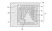
- FIG. 3 is a partial schematic diagram illustrating an example of a first conductive pattern of the flexible printed wiring board (first wiring board) according to the first embodiment of the present invention.
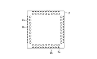
- FIG. 4 is an overall schematic diagram illustrating an example of a bare chip mounted on a first wiring board.
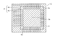
- FIG. 5 is a partial schematic diagram illustrating an example of a first conductive pattern of a flexible printed wiring board (conventional wiring board) according to the related art. It is a partial schematic diagram showing an example of the 2nd conductive pattern of the flexible printed wiring board (3rd wiring board) concerning a 3rd embodiment of the present invention. It is a partial sectional view showing an example of a flexible printed wiring board (fourth wiring board) concerning a fourth embodiment of the present invention.
- FIG. 1 is an overall sectional view showing an example of a pressure sensor having a joined body according to the present invention.
- the flexible printed wiring board according to the first embodiment of the present invention includes an insulating substrate 3, one or more first conductive patterns 4, Is a flexible printed wiring board having:
- the insulating substrate 3 includes a first surface 3a which is a surface on which the bare chip 2 is mounted, and a second surface 3b which is a surface opposite to the first surface 3a.
- the first conductive pattern 4 is provided on the first surface 3a, and is disposed at a position capable of conducting with the bump 2a of the bare chip 2 in a mounting state in which the bare chip 2 is mounted on the first surface 3a.
- One electrode section 4a is included.
- the first conductive pattern 4 is provided only inside the mounting region 3c which is a region facing the bare chip 2 in the mounting state described above.
- FIG. 1 is a partial schematic view showing an example of the first conductive pattern 4 of the first wiring board 1a.
- a portion indicated by hatching represents the insulating substrate 3
- a portion indicated by white represents a portion provided with the first conductive pattern 4.
- FIG. 1 shows an enlarged portion of the first wiring board 1a where the first conductive pattern 4 is provided.
- the insulating substrate 3 is a thin film made of a flexible insulating material.
- a material forming the insulating substrate 3 for example, polyester or polyimide can be used. Since polyester is a thermoplastic material, when polyester is used as a material for forming the insulating substrate 3, it is preferable to perform wiring at room temperature using a conductive paste or the like.
- polyimide has heat resistance, when polyimide is used as a material forming the insulating substrate 3, wiring can be performed by pressure bonding with heating.
- the thickness of the insulating substrate 3 is 10 ⁇ m or more, sufficient strength can be obtained, and when the thickness is 80 ⁇ m or less, excellent flexibility is obtained. Therefore, the thickness is preferably 10 ⁇ m or more and 80 ⁇ m or less. More preferably, the thickness of the insulating substrate 3 is 20 ⁇ m or more and 40 ⁇ m or less.
- the insulating substrate 3 includes a first surface 3a on which the bare chip 2 is mounted and a second surface 3b which is a surface opposite to the first surface 3a. Since the first wiring board 1a is used for mounting the bare chip 2 on the surface thereof, the first surface 3a and the second surface 3b of the insulating substrate 3 are determined based on whether the bare chip 2 is mounted. Are distinguished.
- the first surface 3a and the second surface 3b correspond to the front and back of the same insulating substrate 3, and have the same area and shape.
- the area of the first surface 3a and the second surface 3b of the insulating substrate 3 needs to be at least an area corresponding to the mounting area 3c of the bare chip 2 described later.
- the shape of the first wiring board 1a is not particularly limited.
- the number of bare chips 2 mounted on the first surface 3a of the insulating substrate 3 may be one, or may be two or more.
- the first wiring board 1a plays a role of a wiring for electrically connecting the bare chips 2 to external electrodes and the like.
- the first wiring board 1a can also play the role of wiring for electrically connecting the electrodes of the plurality of bare chips 2 in addition to the role described above.
- the first conductive pattern 4 is provided on the first surface 3a of the insulating substrate 3 and is arranged at a position where the first conductive pattern 4 can be electrically connected to the bump 2a of the bare chip 2 in a mounting state in which the bare chip is mounted on the first surface.
- the first conductive pattern 4 is made of a metal foil having excellent flexibility and electrical conductivity.
- a material forming the first conductive pattern 4 for example, copper, silver, gold, or aluminum can be used. Among these materials, copper is preferable because it is relatively inexpensive and easy to process such as plating and etching. Examples of a method for producing such a metal foil include a rolling method and an electrolytic method.
- For the first wiring board 1a it is preferable to use, for example, a rolled copper foil rich in extensibility.
- the thickness of the first conductive pattern 4 is 5 ⁇ m or more, sufficient conductivity and strength can be obtained, and when the thickness is 20 ⁇ m or less, the flexibility is excellent. Therefore, the thickness is preferably 5 ⁇ m or more and 20 ⁇ m or less. . A more preferable thickness of the first conductive pattern 4 is 7 ⁇ m or more and 12 ⁇ m or less.
- the first conductive pattern 4 can be formed by a known process in a method of manufacturing a flexible printed wiring board, that is, each process of forming a photosensitive resist layer, exposing, etching, and removing the photosensitive resist layer.
- FIG. 2 is an overall schematic diagram showing an example of the bare chip 2 mounted on the first wiring board 1a.
- the bare chip 2 illustrated in FIG. 2 is a plate-like chip having a square shape cut out from a wafer by dicing. As described above, the cut surface of the bare chip 2 cut by dicing is exposed, and the insulating film is not usually formed on the surface. Electrodes (not shown) are exposed on the surface of the bare chip 2 shown in FIG. 2, and bumps 2a are formed on the surface of each electrode so as to protrude from the surface.
- FIG. 2 illustrates the shapes and positions of the bumps 2a. In the example shown in FIG. 2, nine bumps 2a are arranged along each side of the bare chip 2 for a total of 36 bumps 2a.
- the first conductive pattern 4 illustrated in FIG. 1 includes 36 first electrode portions 4a, nine in total along each side of the mounting area 3c of the bare chip 2. These first electrode portions 4a are arranged at positions where they can be electrically connected to the bumps 2a of the bare chip 2. More specifically, the first electrode portion 4a is located at a position facing the bump 2a of the bare chip 2 shown in FIG. 2, that is, a state where the bare chip 2 is mounted on the first surface 3a of the insulating substrate 3 (mounting state). Is provided at a position where the distance from the bump 2a is shortest.
- first electrode portions 4a For ten of the 36 first electrode portions 4a, elongated conductive patterns 4c extending from the position of the first electrode portion 4a toward the center of the mounting region 3c are formed. That is, these ten first conductive patterns 4 are constituted by the elongated conductive patterns 4c and the first electrode portions 4a. The remaining 26 first conductive patterns 4 are each constituted only by the first electrode portion 4a. Note that, in FIG. 1, a portion denoted by reference numeral "3d" will be described later in a description of another embodiment of the present invention.
- first conductive pattern 4 illustrated in FIG. 1 among the 36 first electrode portions 4 a, it is possible to exchange electric signals with the bumps 2 a of the bare chip 2 because of the above-described elongated conductive pattern. There are only 10 connected to 4c. The remaining 26 first electrode portions 4a merely conduct with the bumps 2a of the bare chip 2 and do not have the function as the original electrodes. However, by providing the first electrode portions 4a at all positions facing the bumps 2a of the bare chip 2, the flexible printed wiring board 1a and the bare chip 2 can be bonded in a well-balanced manner.
- a first electrode portion 4a that is electrically connected to the bump 2a of the bare chip 2 is provided along each side of the mounting region 3c of the bare chip 2.
- the position where the first electrode unit 4a is provided is not limited to the position illustrated in FIG.
- the bump 2a of the bare chip 2 is provided at the center of the mounting area 3c
- the first electrode portion 4a can also be provided at the center facing the bump 2a.
- the above-described elongated conductive pattern 4c may be formed so as to extend outward from the center.
- the first conductive pattern 4 is provided only inside the mounting area 3c of the bare chip 2.
- the mounting area 3c of the bare chip 2 is an area on the first surface 3a of the insulating substrate 3 and means an area where the bare chip 2 is to be mounted on the flexible printed wiring board 1a. That is, the mounting area 3c is an area facing the bare chip 2 in the mounting state described above. More precisely, the mounting area 3c is perpendicular to the first surface 3a in a state where the bare chip 2 is arranged at a position where the bare chip 2 is to be mounted on the first surface 3a (that is, the mounting state).
- the shape of the outer periphery of the mounting area 3c corresponding to the contour of the bare chip 2 is represented by a broken line.
- the first conductive pattern 4 is provided only in the mounting area 3c illustrated in FIG. 1, that is, only in the area surrounded by the broken line. In other words, the first conductive pattern 4 is not provided on the first surface 3a outside the mounting area 3c.
- FIG. 3 is a partial schematic view showing an example of a first conductive pattern of a flexible printed wiring board according to the related art (hereinafter, may be referred to as a “conventional wiring board”).
- the position of the bump 2a of the bare chip 2 mounted on the conventional wiring board 1 'shown in FIG. 3 is the same as the position of the bump 2a of the bare chip 2 mounted on the first wiring board 1a shown in FIG. Therefore, also in the conventional wiring board 1 ', a total of 36 first electrode portions 4a' are provided along each side of the mounting area 3c, as in the case of FIG.
- the first conductive pattern 4c 'of the conventional wiring board 1' is an elongated conductive pattern 4c 'so as to protrude outside the mounting area 3c of the bare chip 2. Is provided.
- the bump 2a of the bare chip 2 and the first electrode portion 4a' of the first conductive pattern 4 ' are provided inside the mounting area 3c.
- the conventional wiring board 1 ' is not fixed as tightly as inside the mounting area 3c outside the mounting area 3c, and thus is easily bent. This situation is completely the same in the case of the first wiring board 1a shown in FIG.
- the conventional wiring board 1 'shown in FIG. 3 when the conventional wiring board 1' is bent outside the mounting region 3c, a portion of the first conductive pattern 4 'protruding outside the mounting region 3c. There is a possibility that the bare chip 2 may malfunction due to contact with the edge of the bare chip 2.
- the first conductive pattern 4 is provided only inside the mounting area 3c. Therefore, even when the first wiring board 1a is bent outside the mounting area 3c, there is no possibility that the first conductive pattern 4 comes into contact with the edge of the bare chip 2. Therefore, according to the first wiring board 1a, it is possible to reliably prevent the malfunction of the bare chip 2 due to unexpected conduction.
- the flexible printed wiring board according to the second embodiment of the present invention (hereinafter, sometimes referred to as “second wiring board”) is the above-described first wiring board, in which the bare chip 2 includes the test electrode 2b. It is a flexible printed wiring board provided with. Further, in the second wiring board, the first conductive pattern 4 is provided so as to avoid a position facing the test electrode 2b.
- the test electrode 2b is an electrode provided for the purpose of, for example, checking the operation of a wafer in the middle of a manufacturing process. By bringing the probe into contact with the test electrode 2b, it is possible to measure the electrical characteristics and the like of the devices formed in the wafer and to sort out defective products.
- the test electrode 2b is usually provided at a portion where the wafer is cut by dicing. This is because it is necessary to secure a certain size to the test electrode in order for the probe to be in contact therewith. Therefore, when the test electrode 2b is provided in the portion where the elements of the integrated circuit are formed, the degree of integration of the circuit is increased. Is to be reduced.
- the test electrode 2b is usually located at a portion near the edge of the surface of the bare chip 2. Referring again to FIG. 2, in the bare chip 2 illustrated in FIG. 2, the test electrode 2b is arranged at a position near the edge in a region between the edge of the bare chip 2 and the bump 2a.
- the bare chip 2 includes the test electrode 2b
- the first conductive pattern 4 is bent when the flexible printed wiring board 1a is bent outside the mounting region 3c.
- a portion of the conductive pattern 4 provided at a position facing the test electrode 2b may come into contact with the test electrode 2b and cause a malfunction of the bare chip 2.
- the insulating film does not exist at the position facing the bump 2a and the test electrode 2b is not provided. It is technically difficult to accurately provide an insulating coating so that the insulating coating exists only at the opposing position.
- the first conductive pattern 4 is provided avoiding the position facing the test electrode 2b.
- the first conductive pattern 4 illustrated in FIG. 1 is provided at a position slightly away from the edge, avoiding a position facing the test electrode 2b illustrated in FIG. That is, the first wiring board 1a illustrated in FIG. 1 is a flexible printed wiring board having the features of the second wiring board as described above.
- the test electrode 2b When the test electrode 2b is provided in a region other than the region near the edge of the bare chip 2 unlike the case shown in FIGS. 1 and 2, the position facing the region where the test electrode 2b is provided is determined.
- the first conductive pattern 4 may be provided to avoid this.
- the flexible printed wiring board according to the third embodiment of the present invention (hereinafter, sometimes referred to as “third wiring board”) is the above-described first wiring board or second wiring board, and is an insulating substrate.
- 3 is a flexible printed wiring board having one or two or more through holes 3d formed in 3 and a second conductive pattern 5 provided on the second surface 3b. Further, in the third wiring board, the first conductive pattern 4 and the second conductive pattern 5 are conductive through the through hole 3d.
- FIG. 4 is a partial schematic view showing an example of the second conductive pattern 5 of the third wiring board 1c.
- a portion indicated by oblique lines represents the insulating substrate 3
- a portion indicated by white represents a portion where the second conductive pattern 5 is provided.
- FIG. 4 is a drawing when the same range as the first conductive pattern 4 shown in FIG. 1 is observed from the back side of the insulating substrate 3 (the side opposite to the first surface 3a), that is, from the side of the second surface 3b. is there.
- Through hole 3d is one or more through holes formed in insulating substrate 3.
- the through hole 3d is provided in a region where the first conductive pattern 4 shown in FIG. 1 and the second conductive pattern 5 shown in FIG. 4 overlap. Since the first conductive pattern 4 is provided only inside the mounting area 3c, the position where the through hole 3d is provided is necessarily inside the mounting area 3c.
- the through hole 3d shown in FIGS. 1 and 4 is located at the end of the ten elongated conductive patterns 4c shown in FIG. 1 on the side where the first electrode portion 4a is not provided. Ten are provided.
- the through hole 3d can be formed by means such as a drill. It is preferable that the bonding between the insulating substrate 3 and the first and second conductive patterns 4 and 5 is maintained at the position of the formed through hole 3d.
- the second conductive pattern 5 is provided on the second surface 3 b of the insulating substrate 3. Since the third wiring board includes the second conductive pattern 5, it becomes a double-sided flexible printed wiring board having conductive patterns on both surfaces of the insulating substrate 3.
- the material for forming the second conductive pattern 5, the preferred thickness, and the process of forming the pattern are the same as in the case of the first conductive pattern 4, and a description thereof will be omitted.
- a part of the second conductive pattern 5 illustrated in FIG. 4 includes ten elongated conductive patterns 5d extending from the positions of the ten through holes 3d to the outside of the mounting region 3c (not shown).
- the second conductive pattern 5 does not need to be provided only inside the mounting area 3c, and can be provided outside the mounting area 3c.
- the second surface 3b on which the second conductive pattern 5 is provided is located on the side opposite to the first surface 3a on which the bare chip 2 is mounted. For this reason, even if the second conductive pattern 5 is provided so as to protrude outside the mounting region 3c, there is no possibility that the second conductive pattern 5 contacts the edge of the bare chip 2 when the flexible printed wiring board 1 is bent.
- 26 dummy electrodes 5c are formed at positions where the elongated conductive patterns 5d are not formed. Since the dummy electrode 5c is insulated from the first conductive pattern 4 by the insulating substrate 3, it does not have a function as an electrode. The dummy electrode 5c is provided for the purpose of making the connection between the flexible printed wiring board 1 and the bare chip 2 more reliable. Details of the dummy electrode 5c will be described later. Further, of the ten elongated conductive patterns 5d constituting a part of the second conductive pattern 5, a portion corresponding to the back surface of the first electrode portion 4a also has the same effect as the dummy electrode 5c.
- the portions corresponding to the back surfaces of the first electrode portions 4a are also regarded as the dummy electrodes 5c. That is, the second conductive pattern 5 includes 26 conductive patterns including only the dummy electrodes 5c, and a conductive pattern including a portion regarded as the dummy electrode 5c and the elongated conductive pattern 5d.
- the first conductive pattern 4 and the second conductive pattern 5 are electrically connected via the through hole 3d.
- the insulating substrate 3 separating the first conductive pattern 4 and the second conductive pattern 5 has been removed.
- the first conductive pattern 4 and the second conductive pattern 5 can be conducted through the through hole 3d.
- a known means such as a jumper wire, a hook, a conductive paste, or plating can be employed.
- the first conductive pattern 4 electrically connected to the bump 2a of the bare chip 2 and the second conductive pattern 5 provided on the second surface 3b of the insulating substrate 3 are provided inside the mounting area 3c. It can be made conductive through the provided through hole 3d. All of these conductive patterns are provided around the outside of the mounting area 3c of the first surface 3a of the insulating substrate 3, that is, the area where there is a possibility of contact with the edge of the bare chip 2. Therefore, according to this configuration, it is possible to transmit and receive the electric signal between the bare chip 2 and another device or the like while reliably preventing the malfunction of the bare chip 2 due to unexpected conduction.
- the flexible printed wiring board according to the fourth embodiment of the present invention (hereinafter, may be referred to as “fourth wiring board”) is the third wiring board described above, wherein the first conductive pattern 4 is One or more first lands 4b are provided, and the second conductive pattern 5 is provided with one or more second lands 5b. Further, the first land 4b and the second land 5b are electrically connected via the through hole 3d.
- FIG. 1 shows an example of the first land 4b
- FIG. 4 shows an example of the second land 5b.
- Land is a term indicating a conductive pattern for soldering which is originally provided around the surface of a hole into which a lead wire of a through-hole mounting component is inserted, and has, for example, a circular or square shape.
- the conductive pattern provided around the surface of the through hole 3d provided for conduction between the first conductive pattern 4 and the second conductive pattern 5 is referred to as "land". Called.
- the first land 4b illustrated in FIG. 1 is a circular conductive pattern provided around the opening of the through hole 3d in the first surface 3a of the first conductive pattern 4.
- the second land 5b illustrated in FIG. 4 is a circular conductive pattern provided around the opening of the through hole 3d in the second surface 3b of the second conductive pattern 5.
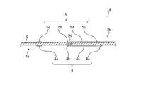
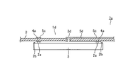
- FIG. 5 is a partial sectional view showing an example of the fourth wiring board.
- the first conductive pattern 4 includes a first land 4b
- the second conductive pattern 5 includes a second land 5b.
- the first land 4b and the second land 5b are electrically connected via the through hole 3d.
- the first land 4b and the second land 5b are electrically connected by providing a plating layer over the inner peripheral surface of the first land 4b, the second land 5b, and the through hole 3d. I have.
- means for ensuring conduction between the first land 4b and the second land 5b via the through hole 3d is not limited to this.
- first land 4b and the second land 5b are joined by a jumper wire inserted through the through hole 3d, a diaper is fitted into the through hole 3d, or a conductive paste is filled in the through hole 3d. By doing so, the first land 4b and the second land 5b can be conducted through the through hole 3d.
- the width of the conductive pattern around the opening of the through hole 3d can be increased.
- the first conductive pattern 4 and the second conductive pattern 5 can be more reliably made conductive.
- the area where the plated conductor contacts the conductive pattern increases due to the presence of the land.
- the electrical resistance of the conductive portion is reduced, and the reliability in mounting the bare chip 2 on the flexible printed wiring board 1 can be increased.
- the mounting area on the first surface is The first conductive pattern is provided only inside. Therefore, even when the wiring board of the present invention is bent outside the mounting area, the first conductive pattern does not contact the edge of the bare chip, so that malfunction of the bare chip due to unexpected conduction can be reliably prevented.
- the second conductive pattern is provided on the second surface, and the first conductive pattern and the second conductive pattern are formed through the through holes. Conducted.
- the second conductive pattern is disposed on the opposite side (that is, the second surface) from the first surface on which the bare chip is mounted. Therefore, for example, as illustrated in FIG. 4, even when the second conductive pattern extends to the outside of the mounting area on the second surface, the second conductive pattern does not correspond to the bare chip when the flexible printed wiring board is bent. There is no risk of contact with the edge.
- the flexible printed wiring board 1 when the flexible printed wiring board 1 is largely bent as illustrated in FIG. 12, for example, conduction between the second conductive pattern 5 and a peripheral member (for example, a storage case or an elastic member) may occur.
- the conductive patterns 5 may be electrically connected to each other, and the bare chip 2 may cause an unexpected malfunction.
- a flexible printed wiring board according to the fifth embodiment of the present invention (hereinafter, may be referred to as a “fifth wiring board”) is the above-described third wiring board or fourth wiring board.
- the flexible printed wiring board further includes an insulating layer provided so as to cover at least a part of the two conductive patterns.
- the material constituting the insulating layer is an insulating material capable of reducing unexpected conduction between the second conductive pattern and another member and / or unexpected conduction between the second conductive patterns.
- the insulating layer may be a thin film made of a flexible insulating material, similarly to the above-described insulating substrate.
- the insulating layer can be provided in a predetermined region by attaching such a film with an adhesive.
- a material constituting such a film for example, polyester or polyimide can be given.
- the insulating layer may be an insulating film (resist) made of an insulating material applied to a predetermined region.
- the region where the insulating layer is provided is also a region where unexpected conduction between the second conductive pattern and other members as described above and / or unexpected conduction between the second conductive patterns can be reduced.
- the insulating layer may be provided only in a region where unexpected conduction between the second conductive pattern and another member and / or unexpected conduction between the second conductive patterns may occur.
- a portion of the second conductive pattern except for a portion where electrical connection between the second conductive pattern and another member is performed for example, around an opening of a through hole, a second land, and a second electrode portion described later).
- the insulating layer may be provided on all surfaces.
- the insulating layer may be provided on all surfaces of the second surface except for a portion where the second conductive pattern is electrically connected to another member.
- the thickness and the constituent material of the insulating layer may be, for example, in accordance with the characteristics (eg, flexibility, heat resistance, wear resistance, etc.) required for the fifth wiring board in the application to which the fifth wiring board is applied. Accordingly, it can be determined appropriately.
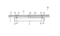
- FIG. 6 is a partial sectional view showing an example of the fifth wiring board.
- the fifth wiring board 1e illustrated in FIG. 6 has the same configuration as that of FIG. 5 except that the fifth wiring board 1e further includes an insulating layer 10 (a portion hatched to the lower right) provided on the entire second surface 3b of the insulating substrate 3. It has the same configuration as the fourth wiring board 1d exemplified.
- a four-layer structure including the first conductive pattern 4, the insulating substrate 3, the second conductive pattern 5, and the insulating layer 10 is provided. Are formed.
- the insulating layer 10 is formed of the same polyimide film as the insulating substrate 3, and is coated with an adhesive so as to cover the entire surface of the second surface 3b except for an electrode portion (not shown). Joined (pasted). Note that the thickness of the insulating layer 10 shown in this example is about half (for example, 12.5 ⁇ m) of the thickness of the insulating substrate 3 and, for example, the pressure sensor 8 shown in FIG. Has been confirmed.
- the fifth wiring board 1e is a flexible printed wiring board further including the insulating layer 10 provided so as to cover at least a part of the second conductive pattern 5.
- the second conductive pattern 5 may come into contact with a peripheral member (for example, a storage case or an elastic member), or The possibility that the two conductive patterns 5 come into contact with each other can be reduced.
- unexpected malfunction of the bare chip 2 due to unexpected conduction caused by contact between the second conductive pattern 5 and peripheral members and / or contact between the second conductive patterns 5 as described above is reduced. be able to.
- the contact between the second conductive pattern 5 and the peripheral member and / or the contact between the second conductive patterns 5 does not occur.
- the distance between the patterns 5 may be significantly reduced due to the bending of the flexible printed wiring board.
- a discharge occurs between the second conductive pattern 5 and a peripheral member and / or between the second conductive patterns 5, and a bare chip caused by the discharge is generated.
- an unexpected malfunction of 2, etc. may occur.
- the rigidity of the flexible printed wiring board can be increased by further providing the insulating layer 10.
- the flexible printed wiring board according to the sixth embodiment of the present invention (hereinafter sometimes referred to as “sixth wiring board”) is any of the above-described third to fifth wiring boards.
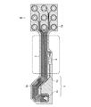
- the second conductive pattern 5 is a flexible printed wiring board including a second electrode portion 5 a for conducting with the external electrode 6.
- FIG. 7 is an overall schematic diagram illustrating an example of the sixth wiring board 1f.
- FIG. 7 shows the second conductive pattern 5 provided on the second surface 3 b side of the insulating substrate 3.
- the positions of the nine second electrode portions 5a are shown on the right side of the sixth wiring board 1f shown in FIG.
- a through hole is provided in each of the second electrode portions 5a, and an external electrode 6 (not shown) is inserted into the through hole.
- the external electrode 6 and the second electrode portion 5a can be electrically connected by a known means such as soldering.
- the second electrode portion 5a can be provided according to the size of the external electrode 6. By providing the second electrode portion 5a, for example, even when the size of the region where the external electrodes 6 are arranged is significantly larger than the size of the region where the bumps 2a of the bare chip 2 are arranged, the bump 2a of the bare chip 2 Conduction with the external electrode 6 can be ensured. In the example shown in FIG. 7, nine of the ten second lands 5b and nine of the second electrode portions 5a are individually separated by nine elongated conductive patterns 5d constituting the second conductive pattern 5. Is conducted.
- the distance between the second land 5b and the second electrode portion 5a is long, and the distance between the second conductive pattern and the second conductive pattern located at the center of the sixth wiring board 1f is increased.
- the part (the part surrounded by the broken line) can be bent freely.
- a protection plate (support plate) made of a rigid body (not shown) or the like can be provided for the purpose of, for example, facilitating assembly with the external electrode 6.
- nine elongated conductive patterns 5d for electrically connecting the second land 5b and the second electrode 5a are provided from the inside to the outside of the mounting region 3c (not shown). At this time, these elongated conductive patterns 5d do not extend in a direction parallel to the direction connecting the second lands 5b and the second electrodes 5a, but connect the second lands 5b and the second electrodes 5a. It extends in a direction perpendicular to the connecting direction, that is, in the upper direction in FIG.
- the sixth wiring board 1f When the sixth wiring board 1f is bent in the left-right direction in FIG. 7, the sixth wiring board 1f hardly bends in the vertical direction in FIG. In other words, when the sixth wiring board 1f is bent around the axis extending in the vertical direction in FIG.
- the sixth wiring board 1f does not bend around the axis extending in the left-right direction in FIG. Therefore, by extending the elongated conductive pattern 5d of the second conductive pattern 5 in the direction perpendicular to the linear direction connecting the second land 5b and the second electrode 5a, the left and right directions of the sixth wiring board 1f are extended. Malfunction of the bare chip 2 due to bending can be more reliably prevented.
- one of the ten second lands 5b is electrically connected to the chip resistor 9 via one elongated conductive pattern 5d.
- the chip resistor 9 has a role of adjusting the voltage of a control signal supplied from the external electrode 6 (not shown) and applying the control signal to the bare chip 2. This control signal is used, for example, for the purpose of switching the operation mode of the bare chip 2 or fixing the operation mode.
- Such a chip resistor 9 can be provided not only in the sixth wiring board 1f but also in the wiring boards of the present invention according to various embodiments.
- a portion of the wiring board of the present invention where the chip resistor 9 is provided is not shown for the purpose of, for example, preventing breakage of the chip resistor 9 and / or release of conduction (disconnection) due to excessive bending.
- a protection plate (support plate) or the like made of a rigid body can be provided.
- the present invention is limited to only the flexible printed wiring boards (the present invention wiring board) according to various embodiments of the present invention including the above-described first to sixth wiring boards.
- the present invention also relates to a joined body comprising the wiring board of the present invention and a bare chip.
- the joined body according to the seventh embodiment of the present invention (hereinafter, may be referred to as a “seventh joined body”) may be any one of the first to sixth wiring boards 1a to 1f described above. It is a joined body composed of a wiring board and a bare chip.
- the wiring board of the present invention is created on the assumption that one or two or more bare chips 2 are mounted on the first surface 3a.
- the joined body according to the present invention (the joined body of the present invention) is a composite in which a bare chip is actually mounted on the wiring board of the present invention.
- the portion of the flexible printed wiring board has the above-described configuration of the wiring board of the present invention. Therefore, by bonding the bare chip 2 thereto, the same operation and effect as those of the wiring board of the present invention can be obtained.
- FIG. 8 is a partial cross-sectional view showing an example of a seventh joined body 7a composed of the fourth wiring board 1d and the bare chip 2 illustrated in FIG. 5 among the wiring boards of the present invention according to various embodiments.
- a joint portion between the flexible printed wiring board 1 and the bare chip 2 is illustrated in an enlarged manner.
- the bump 2a of the bare chip 2 and the first electrode portion 4a of the first conductive pattern 4 provided at a position facing the bump 2a are electrically connected to each other, and are joined at least at the electrically conductive portion.
- a conductive paste, solder, or other known means can be adopted as means for electrically connecting the bump 2a and the first electrode portion 4a.
- a conductive paste, solder, or other known means can be adopted as described above, as means for securing conduction between the first land 4b and the second land 5b through the through hole 3d, for example, means such as a jumper wire, a staple, a conductive paste or plating, not shown. Can
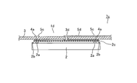
- FIG. 9 is a partial cross-sectional view showing an example of a seventh joined body 7b composed of the fifth wiring board 1e and the bare chip 2 illustrated in FIG. 6 among the wiring boards of the present invention according to various embodiments.
- a fifth wiring board 1e instead of the fourth wiring board 1d, a fifth wiring board 1e further including an insulating layer 10 provided so as to cover at least a part of the second conductive pattern 5 is used as the flexible printed wiring board. ing.
- the second conductive pattern 5 and peripheral members are electrically connected, and the second conductive patterns 5 are electrically connected to each other. It is possible to reduce the risk of occurrence. As a result, it is possible to reduce a possibility that the bare chip 2 may cause an unexpected malfunction due to the unexpected conduction as described above.
- the rigidity of the fifth wiring board 1e can be increased by further providing the insulating layer 10. Therefore, in the seventh joined body 7b, the bending due to the bending of the fifth wiring board 1e is suppressed, and the second conductive pattern 5 and the peripheral members are excessively approached and / or the second conductive pattern 5 are excessively approached to each other. Can be prevented. As a result, for example, even when noise or the like having a high voltage occurs, the occurrence of discharge between the second conductive pattern 5 and peripheral members and / or between the second conductive patterns 5 is reduced, and the discharge is reduced. This can reduce unexpected malfunctions and the like of the bare chip 2 caused by the above.
- the joined body according to the eighth embodiment of the present invention (hereinafter, may be referred to as an “eighth joined body”) is the above-described seventh joined body, and includes the bump 2a and the first electrode unit 4a. Is achieved by an anisotropic conductive film (ACF).
- the anisotropic conductive film is a film in which a thermosetting resin in which metal fine particles having an insulating layer on the surface are mixed and dispersed is formed into a film shape.
- a dummy electrode 5c is provided on the back side of the first electrode portion 4a (that is, the second surface 3b opposite to the first surface 3a). ing.
- an anisotropic pinched between the bump 2a and the first electrode portion 4a is provided, as compared with the case where the dummy electrode 5c is not provided.
- the pressure applied to the conductive film 2c increases locally. Thereby, conduction by the anisotropic conductive film 2c can be realized more reliably.
- an insulating coating can be provided on a portion of the surface of the bare chip 2 other than the bumps 2a.
- an insulating coating may be further provided on at least a part (for example, a part surrounded by the first electrode part 4a) of the mounting area on the first surface 3a except the first electrode part 4a.
- the present invention provides a flexible printed wiring board (the present wiring board) and a flexible printed wiring board according to various embodiments of the present invention including the above-described first to sixth wiring boards.
- the present invention relates not only to the joined bodies according to various embodiments of the present invention including the seventh joined body and the eighth joined body (the joined body of the present invention), but also to a pressure sensor having the joined body of the present invention.
- the pressure sensor according to the ninth embodiment of the present invention (hereinafter, may be referred to as a “ninth sensor”) is a pressure sensor according to the present invention including the above-described seventh bonded body or eighth bonded body.
- a pressure sensor, wherein the bare chip is a strain sensor.
- FIG. 12 is an overall sectional view showing an example of a pressure sensor 8 as a ninth sensor having the joined body of the present invention.
- the pressure sensor 8 includes a diaphragm that defines a space that communicates with a flow path of a fluid whose pressure is to be measured.
- a bare chip 2 as a strain sensor is joined to the surface of the diaphragm or an elastic member mechanically joined to the diaphragm. By detecting the deformation of the diaphragm caused by the pressure of the fluid by the strain sensor, the pressure of the fluid can be measured.
- the bare chip 2 as a strain sensor for example, a strain sensor having a plurality of resistance elements described in Patent Document 4 or the like can be used.
- an absolute pressure sensor that is not affected by the atmospheric pressure outside the pressure sensor 8 can be realized.
- a wiring board of the present invention such as the sixth wiring board 1f illustrated in FIG. 7 can be used, for example.
- the joined body of the present invention composed of both can be assembled.
- the flexible printed wiring board 1 is largely bent and inserted into a narrow space of the storage case.
- the pressure sensor 8 shown in FIG. 12 can be assembled.
- the first conductive pattern 4 is provided only in the mounting area 3c of the bare chip 2 on the first surface 3a of the insulating substrate 3 constituting the wiring board of the present invention as the flexible printed wiring board 1. Is not provided with a conductive pattern.
- the second conductive pattern 5 is provided on the second surface 3b of the insulating substrate 3 opposite to the first surface 3a. Therefore, no matter how the flexible printed wiring board 1 bends, the first conductive pattern 4 and the second conductive pattern 5 do not conduct to the edge of the bare chip 2. Thus, a highly reliable pressure sensor 8 can be manufactured.
- the present invention relates to a flexible printed wiring board (the present wiring board) according to various embodiments of the present invention including the above-described first to sixth wiring boards, A bonded body according to various embodiments of the present invention including the seventh bonded body and the eighth bonded body (the bonded body of the present invention) and a sensor according to various embodiments of the present invention including the ninth sensor (the present invention) Sensor) as well as a mass flow controller having the sensor of the invention.
- the mass flow control device according to the tenth embodiment of the present invention (hereinafter, may be referred to as a “tenth device”) includes the ninth sensor and other present sensors as pressure sensors. And a mass flow controller for monitoring the pressure of the fluid by the pressure sensor.
- the device of the present invention includes, for example, a fluid flow path provided in a body, a means for monitoring the flow rate of the fluid flowing through the flow path, and a sensor of the present invention (for example, a pressure sensor 8) as a means for monitoring the pressure of the fluid. And means for controlling the flow rate of the fluid.
- the sensor of the present invention may constitute a part of a means for monitoring the flow rate of the fluid. According to the present invention, by accurately monitoring the pressure of the fluid using the mass flow controller incorporating the highly reliable sensor of the present invention, the measurement accuracy of the flow rate of the fluid can be increased, and the pressure fluctuation can be reduced. Accordingly, it is possible to accurately control the flow rate of the fluid.
- the sixth wiring board 1f illustrated in FIG. 7 was adopted as a flexible printed wiring board, and the bare chip illustrated in FIG. 2 was adopted as a strain sensor.
- the bare chip 2 having no test electrode 2b on the surface on which the bump 2a is provided is employed.
- the bare chip 2 having the test electrode 2b on the surface on which the bump 2a is provided is employed. It was adopted.
- Comparative Example 1 the flexible printed wiring board according to the prior art illustrated in FIG. 3 (conventional wiring board 1 ′) was employed as a flexible printed wiring board, and the bare chip 2 illustrated in FIG. 2 was employed as a strain sensor. .
- the bare chip 2 having no test electrode 2b on the surface provided with the bump 2a and the bare chip 2 having the test electrode 2b on the surface provided with the bump 2a were mixed.
- the first conductive pattern is provided only inside the mounting area 3c of the first surface 3a of the flexible printed wiring board, whereas in the comparative example 1, the flexible printed wiring board is provided.
- the first conductive pattern is provided not only inside the mounting area 3c of the first surface 3a but also outside the mounting area 3c.
- the shape of the mounting area 3c of the bare chip 2 was a square having a side of 2.5 mm.
- Examples 1 and 2 after printing a resist pattern corresponding to the first conductive pattern 4 illustrated in FIG. 1 and the second conductive pattern 5 illustrated in FIG. The foil was removed by etching.
- a polyimide film was bonded (attached) to a portion other than the first electrode portion 4a of the first conductive pattern 4 and the second electrode portion 5a of the second conductive pattern 5 with an adhesive. That is, in the sixth wiring board 1f included in the first and second embodiments, the insulating layer 10 included in the fifth wiring board 1e illustrated in FIG. 6 is formed of a polyimide film. Further, a nickel plating layer having a thickness of 1 ⁇ m and a gold plating layer having a thickness of 0.03 ⁇ m were sequentially formed on the surfaces of the first electrode portion 4a and the second electrode portion 5a by electroless plating.
- Comparative Example 1 after the resist pattern corresponding to the first conductive pattern 4 'illustrated in FIG. 3 was printed, unnecessary portions of the rolled copper foil were removed by etching. Next, a resist pattern was printed on portions of the first conductive pattern 4 'other than the first electrode portions 4a'.
- the first pattern is provided near the mounting region 3c. A portion where the conductive pattern 4 'was exposed was formed. Further, on the surface of the first electrode portion 4a ', a nickel plating layer having a thickness of 1 [mu] m was sequentially formed by electroless plating in the same manner as in Example 1 and Example 2.
- the pressure sensors 8 illustrated in FIG. 12 are assembled by using the above-described various flexible printed wiring boards and the bare chips 2, respectively, to thereby obtain Examples 1 and 2 and Comparative Example 1. Each of the evaluation sensors was assembled.
- a diaphragm provided in the main body so as to define a space communicating with a flow path of a fluid to be measured, and an elastic member mechanically joined to the diaphragm. was prepared, and the surface of the bare member 2 where the bumps 2a were not formed was joined to the surface of the elastic member.
- an anisotropic conductive film is placed on the surface of the bare chip 2 on which the bumps 2a are formed, and the bare chip 2 and the mounting area 3c are further overlapped thereon (that is, the bump 2a of the bare chip 2 and the first
- various flexible printed wiring boards were mounted (so that the electrode portion 4a or the first electrode portion 4a 'was opposed).
- a storage case including the external electrodes 6 as illustrated in FIG. 12 is prepared, and the sixth wiring board 1f constituting the joined body according to the first and second embodiments is prepared.
- the two-electrode part 5a and the external electrode 6 were electrically connected.
- Comparative Example 1 an electrode portion (not shown) of the conventional wiring board 1 ′ constituting the joined body was electrically joined to the external electrode 6.
- various kinds of evaluations were performed by assembling the main body including the various joined bodies, the diaphragms and the elastic members into the storage case while bending the various flexible printed wiring boards, and welding the main body and the storage case. Sensor was assembled.
- Table 1 The structures of the evaluation sensors according to Examples 1 and 2 and Comparative Example 1 assembled in this way are listed in Table 1 below.
- the evaluation sensors according to Comparative Example 1 As a result of the electric resistance measurement in the above a) and b), 480 out of 499 evaluation sensors were determined to be “pass”, but the remaining 19 Each of the samples showed a resistance value equal to or lower than the reference value, and thus was judged as "fail". That is, the bare chip 2 is mounted on the flexible printed wiring board (conventional wiring board) according to the related art in which the first conductive pattern is provided not only inside the mounting area 3c on the first surface 3a but also outside the mounting area 3c. In the pressure sensor, it is determined that unexpected conduction has occurred without passing through the bump 2 a between the first conductive pattern 4 ′ and the bare chip 2.
- the welded portion between the main body and the storage case is cut to expose the flexible printed wiring board, and power is supplied to the bare chip 2.
- a test was performed in which the flexible printed wiring board was deformed using tweezers to approach the edge of the bare chip 2.
- a pressure sensor including a conventional wiring board in which the first conductive pattern 4 is provided not only inside the mounting area 3c of the bare chip 2 but also outside the external electrodes that are electrically connected to the conductive pattern of the flexible printed wiring board are provided. It was confirmed that unintended conduction between the external electrode and the unintended conduction between the external electrode and the housing case could not be reliably prevented (insulation evaluation A). In addition, when the flexible printed wiring board was deformed using tweezers to approach the edge of the bare chip 2, it was confirmed that an abnormal operation of the bare chip 2 occurred in all the cases. That is, it has been confirmed that it is difficult to achieve excellent insulation and reliability in a pressure sensor including a conventional wiring board.
Landscapes
- Engineering & Computer Science (AREA)
- Physics & Mathematics (AREA)
- General Physics & Mathematics (AREA)
- Microelectronics & Electronic Packaging (AREA)
- Automation & Control Theory (AREA)
- Manufacturing & Machinery (AREA)
- Structure Of Printed Boards (AREA)
- Wire Bonding (AREA)
Abstract
Description
本発明の第1実施形態に係るフレキシブルプリント配線板(以降、「第1配線板」と称呼される場合がある。)は、絶縁基板3と、1又は2以上の第1導電パターン4と、を有するフレキシブルプリント配線板である。絶縁基板3は、ベアチップ2が実装される表面である第1面3a及び第1面3aの反対側に位置する表面である第2面3bを備える。第1導電パターン4は、第1面3aに設けられ、ベアチップ2が第1面3aに実装された状態である実装状態においてベアチップ2のバンプ2aと導通することが可能な位置に配置された第1電極部4aを含む。更に、第1導電パターン4は、上述した実装状態においてベアチップ2に対向する領域である実装領域3cの内部にのみ設けられている。
本発明の第2実施形態に係るフレキシブルプリント配線板(以降、「第2配線板」と称呼される場合がある。)は、上述した第1配線板であって、ベアチップ2がテスト用電極2bを備えるフレキシブルプリント配線板である。更に、第2配線板においては、第1導電パターン4が、テスト用電極2bに対向する位置を避けて設けられている。
本発明の第3実施形態に係るフレキシブルプリント配線板(以降、「第3配線板」と称呼される場合がある。)は、上述した第1配線板又は第2配線板であって、絶縁基板3に穿たれた1又は2以上のスルーホール3dと、第2面3bに設けられた第2導電パターン5と、を有するフレキシブルプリント配線板である。更に、第3配線板においては、第1導電パターン4と第2導電パターン5とがスルーホール3dを介して導通している。
本発明の第4実施形態に係るフレキシブルプリント配線板(以降、「第4配線板」と称呼される場合がある。)は、上述した第3配線板であって、第1導電パターン4が、1又は2以上の第1ランド4bを備え、第2導電パターン5が、1又は2以上の第2ランド5bを備える。更に、第1ランド4bと第2ランド5bとが、スルーホール3dを介して導通している。図1には第1ランド4bの例が、図4には第2ランド5bの例が、それぞれ示されている。
以上説明してきたように、第1配線板乃至第4配線板を始めとする本発明の種々の実施形態に係るフレキシブルプリント配線板(本発明配線板)においては、第1面上の実装領域の内部にのみ第1導電パターンが設けられている。従って、実装領域の外部において本発明配線板が屈曲した場合においても、第1導電パターンがベアチップのエッジと接触しないので、想定しない導通によるベアチップの誤動作を確実に防止することができる。
本発明の第6実施形態に係るフレキシブルプリント配線板(以降、「第6配線板」と称呼される場合がある。)は、上述した第3配線板乃至第5配線板の何れかであって、第2導電パターン5が、外部電極6と導通するための第2電極部5aを備える、フレキシブルプリント配線板である。図7は、第6配線板1fの例を示す全体模式図である。図7には、絶縁基板3の第2面3b側に設けられた第2導電パターン5が示されている。図7に示す第6配線板1fの左側には、ベアチップ2が実装される部分があり、10個の第2ランド5bの位置が示されている。図7に示す第6配線板1fの右側には、9個の第2電極部5aの位置が示されている。
ところで、本明細書において前述したように、本発明は、上述した第1配線板乃至第6配線板を始めとする本発明の種々の実施形態に係るフレキシブルプリント配線板(本発明配線板)のみならず、本発明配線板とベアチップとからなる接合体にも関する。本発明の第7実施形態に係る接合体(以降、「第7接合体」と称呼される場合がある。)は、上述した第1配線板1a乃至第6配線板1fの何れかの本発明配線板と、ベアチップとからなる、接合体である。本発明配線板は、1個又は2個以上のベアチップ2を第1面3aに実装することを想定して創作されたものである。本発明に係る接合体(本発明接合体)は、本発明配線板にベアチップを実際に実装した複合体である。本発明接合体のうち、フレキシブルプリント配線板の部分は、上述した本発明配線板の構成を備えている。従って、これにベアチップ2を接合することにより、本発明配線板が有する作用・効果と同一の作用・効果を奏することができる。
本発明の第8実施形態に係る接合体(以降、「第8接合体」と称呼される場合がある。)は、上述した第7接合体であって、バンプ2aと第1電極部4aとの導通が異方性導電フィルム(Anisotropic Conductive Film、ACF)によって達成されている接合体である。異方性導電フィルムとは、表面に絶縁層を備える金属微粒子が混合・分散された熱硬化性樹脂が膜状に成形されてなるフィルムである。バンプ2aと第1電極部4aとの間に異方性導電フィルムを挟み、ヒータ等によって加熱しながら圧力を加えると、大きな圧力が加わった部分においてフィルム内に分散されている金属微粒子が互いに接触することにより絶縁が破壊され、導通する経路が形成される。圧力が加わらなかった部分においては絶縁層により導通が妨げられるため、絶縁が保持される。異方性導電フィルムを使用することにより、多数の電極間の導通を一度の加熱及び加圧により実現することができるので、上述した第7接合体7a及び7bを始めとする本発明接合体の製造コストを抑制することができる。
ところで、本明細書において前述したように本発明は、上述した第1配線板乃至第6配線板を始めとする本発明の種々の実施形態に係るフレキシブルプリント配線板(本発明配線板)並びに第7接合体及び第8接合体を始めとする本発明の種々の実施形態に係る接合体(本発明接合体)のみならず、本発明接合体を有する圧力センサにも関する。本発明の第9実施形態に係る圧力センサ(以降、「第9センサ」と称呼される場合がある。)は、上述した第7接合体又は第8接合体を始めとする本発明接合体を有し、ベアチップがひずみセンサである、圧力センサである。
ところで、本明細書において前述したように本発明は、上述した第1配線板乃至第6配線板を始めとする本発明の種々の実施形態に係るフレキシブルプリント配線板(本発明配線板)、第7接合体及び第8接合体を始めとする本発明の種々の実施形態に係る接合体(本発明接合体)並びに第9センサを始めとする本発明の種々の実施形態に係るセンサ(本発明センサ)のみならず、本発明センサを有する質量流量制御装置にも関する。本発明の第10実施形態に係る質量流量制御装置(以降、「第10装置」と称呼される場合がある。)は、上述した第9センサを始めとする本発明センサを圧力センサとして有し、当該圧力センサによって流体の圧力をモニタリングする質量流量制御装置の発明である。
本発明に係るフレキシブルプリント配線板(本発明配線板)及び従来技術に係るフレキシブルプリント配線板(従来配線板)とひずみセンサであるベアチップとを用いて、本発明に係る圧力センサである実施例1及び実施例2並びに従来技術に係る圧力センサである比較例1を評価用センサとしてそれぞれ製造した。
各評価用センサに用いられるフレキシブルプリント配線板の調製手順につき、以下に説明する。先ず、30μmの厚さを有するポリイミドフィルムからなる絶縁基板3の第1面3a及び第2面3bに10μmの厚さを有する圧延銅箔が積層された銅張積層板を用意し、スルーホール3dを穿設した。その後、スルーホールめっき加工処理によりスルーホール3dを介する第1面3a側と第2面3b側との導通が可能な状態を達成した。
次に、上述した各種フレキシブルプリント配線板及びベアチップ2を用いて図12に例示した圧力センサ8をそれぞれ組み立てることにより、実施例1及び実施例2並びに比較例1に係る評価用センサをそれぞれ組み立てた。
次に、図12に例示したような外部電極6を備える収納ケースを用意し、実施例1及び実施例2に係る接合体を構成する第6配線板1fの第2電極部5aと外部電極6とを電気的に接合した。一方、比較例1については、接合体を構成する従来配線板1’の図示しない電極部と外部電極6とを電気的に接合した。次に、図12に例示したように各種フレキシブルプリント配線板を屈曲させながら、各種接合体、ダイアフラム及び弾性部材を含む本体を収納ケースに組み込み、本体と収納ケースとを溶接することにより、各種評価用センサを組み立てた。このようにして組み立てられた実施例1及び実施例2並びに比較例1に係る評価用センサの構成につき、以下の表1に列挙する。

上記のようにして得られた実施例1及び実施例2並びに比較例1に係る評価用センサの各々につき、以下に示すa)及びb)の電気抵抗値測定を行い、検出された電気抵抗値がそれぞれの基準値を超えるものを「合格」、検出された電気抵抗値がそれぞれの基準値以下であるものを「不合格」と判定した。各評価用センサの判定結果もまた表1に列挙されている。
外部電極6のうちベアチップ2のアースと導通している1つの外部電極と他の8つの外部電極との間の電気抵抗をデジタルマルチメータで測定した。
b)外部電極と収納ケースとの間の電気抵抗値測定
上記a)と同じ測定器(デジタルマルチメータ)及び絶縁抵抗計(印加電圧=125V)を用いて、評価用センサの収納ケースと9つの外部電極6との間の電気抵抗を測定した。
次に、テスト用電極を有するベアチップ2及び本発明配線板を備える実施例2に係る評価用センサを実施例3に係る評価用センサとして選択し、テスト用電極の有無が混在するベアチップ2及び従来配線板を備える比較例1に係る評価用センサのうち上記絶縁性評価A(即ち、上記a)及びb)の電気抵抗値測定による評価)において「合格」と判定された個体を比較例2に係る評価用センサとして選択した。
以上の結果から、本発明に係るフレキシブルプリント配線板(本発明配線板)を備える圧力センサにおいては、ベアチップにおけるテスト用電極の有無にかかわらず、優れた絶縁性及び信頼性を達成することができた。このことから、第1導電パターン4がベアチップ2の実装領域3cの内部にのみ設けられる本発明配線板によれば、ベアチップ2のエッジ及びテスト用電極2bとフレキシブルプリント配線板の導電パターンとの意図しない電気的接触及び収容ケースと導電パターンとの意図しない電気的接触を確実に防止することができることが確認された。
1a フレキシブルプリント配線板(本発明の第1実施形態)
1c フレキシブルプリント配線板(本発明の第3実施形態)
1d フレキシブルプリント配線板(本発明の第4実施形態)
1e フレキシブルプリント配線板(本発明の第5実施形態)
1f フレキシブルプリント配線板(本発明の第6実施形態)
1’ フレキシブルプリント配線板(従来技術)
2 ベアチップ
2a バンプ
2b テスト用電極
2c 異方性導電フィルム(ACF)
3 絶縁基板
3a 第1面
3b 第2面
3c 実装領域
3d スルーホール
4 第1導電パターン
4a 第1電極部
4b 第1ランド
4c 細長い導電パターン
4’第1導電パターン(従来技術)
4a’ 第1電極部(従来技術)
4c’ 細長い導電パターン
5 第2導電パターン
5a 第2電極部
5b 第2ランド
5c ダミー電極
5d 細長い導電パターン
6 外部電極
7 接合体(本発明)
7a 接合体(第4配線板1dを含む)
7b 接合体(第5配線板1eを含む)
7c 接合体(第4配線板1d及びACFを含む)
7d 接合体(第5配線板1e及びACFを含む)
8 圧力センサ
9 チップ抵抗
10 絶縁層
Claims (10)
- ベアチップ(2)が実装される表面である第1面(3a)及び前記第1面(3a)の反対側に位置する表面である第2面(3b)を備える絶縁基板(3)と、
前記第1面(3a)に設けられ、前記ベアチップ(2)が前記第1面(3a)に実装された状態である実装状態において前記ベアチップ(2)のバンプ(2a)と導通することが可能な位置に配置された第1電極部(4a)を含む1又は2以上の第1導電パターン(4)と、
を有し、
前記第1導電パターン(4)が、前記実装状態において前記ベアチップ(2)に対向する領域である実装領域(3c)の内部にのみ設けられている、
フレキシブルプリント配線板(1a)。 - 請求項1に記載されたフレキシブルプリント配線板(1a)であって、
前記ベアチップ(2)が、テスト用電極(2b)を備え、
前記第1導電パターン(4)が、前記テスト用電極(2b)に対向する位置を避けて設けられている、
フレキシブルプリント配線板(1a)。 - 請求項1又は請求項2に記載されたフレキシブルプリント配線板(1a)であって、
前記絶縁基板(3)に穿たれた1又は2以上のスルーホール(3d)と、
前記第2面(3b)に設けられた第2導電パターン(5)と、
を有し、
前記第1導電パターン(4)と前記第2導電パターン(5)とが、前記スルーホール(3d)を介して導通している、
フレキシブルプリント配線板(1c)。 - 請求項3に記載されたフレキシブルプリント配線板(1c)であって、
前記第1導電パターン(4)が、1又は2以上の第1ランド(4b)を備え、
前記第2導電パターン(5)が、1又は2以上の第2ランド(5b)を備え、
前記第1ランド(4b)と前記第2ランド(5b)とが、前記スルーホール(3d)を介して導通している、
フレキシブルプリント配線板(1d)。 - 請求項3又は請求項4に記載されたフレキシブルプリント配線板(1c、1d)であって、
前記第2導電パターンの少なくとも一部を覆うように設けられた絶縁層(10)を更に備える、
フレキシブルプリント配線板(1e)。 - 請求項3乃至請求項5の何れか1項に記載されたフレキシブルプリント配線板(1c、1d、1e)であって、
前記第2導電パターン(5)が、外部電極(6)と導通するための第2電極部(5a)を備える、
フレキシブルプリント配線板(1f)。 - 請求項1乃至請求項6の何れか1項に記載されたフレキシブルプリント配線板(1a、1c、1d、1e、1f)と、
ベアチップ(2)と、
からなる、
接合体(7a、7b)。 - 請求項7に記載された接合体(7a、7b)であって、
前記バンプ(2a)と前記第1電極部(4a)との導通が異方性導電フィルムによって達成されている、
接合体(7c、7d)。 - 請求項7又は請求項8に記載された接合体(7)を有し、
前記ベアチップ(2)がひずみセンサである、
圧力センサ(8)。 - 請求項9に記載された圧力センサ(8)を有し、
前記圧力センサ(8)によって流体の圧力をモニタリングするように構成されている、
質量流量制御装置。
Priority Applications (4)
| Application Number | Priority Date | Filing Date | Title |
|---|---|---|---|
| CN201980063086.3A CN112771657B (zh) | 2018-09-25 | 2019-09-20 | 挠性印刷电路板、接合体、压力传感器及质量流量控制装置 |
| KR1020217008465A KR102734462B1 (ko) | 2018-09-25 | 2019-09-20 | 플렉시블 프린트 배선판, 접합체, 압력 센서 및 질량 유량 제어 장치 |
| US17/278,782 US11895776B2 (en) | 2018-09-25 | 2019-09-20 | Flexible printed wiring board, joined body, pressure sensor and mass flow controller |
| JP2020549106A JP7207415B2 (ja) | 2018-09-25 | 2019-09-20 | フレキシブルプリント配線板、接合体、圧力センサ及び質量流量制御装置 |
Applications Claiming Priority (2)
| Application Number | Priority Date | Filing Date | Title |
|---|---|---|---|
| JP2018-178800 | 2018-09-25 | ||
| JP2018178800 | 2018-09-25 |
Publications (1)
| Publication Number | Publication Date |
|---|---|
| WO2020066872A1 true WO2020066872A1 (ja) | 2020-04-02 |
Family
ID=69950089
Family Applications (1)
| Application Number | Title | Priority Date | Filing Date |
|---|---|---|---|
| PCT/JP2019/036907 Ceased WO2020066872A1 (ja) | 2018-09-25 | 2019-09-20 | フレキシブルプリント配線板、接合体、圧力センサ及び質量流量制御装置 |
Country Status (5)
| Country | Link |
|---|---|
| US (1) | US11895776B2 (ja) |
| JP (1) | JP7207415B2 (ja) |
| KR (1) | KR102734462B1 (ja) |
| CN (1) | CN112771657B (ja) |
| WO (1) | WO2020066872A1 (ja) |
Cited By (1)
| Publication number | Priority date | Publication date | Assignee | Title |
|---|---|---|---|---|
| CN112312657A (zh) * | 2020-08-28 | 2021-02-02 | 昆山华冠商标印刷有限公司 | 电路跨线结构及其制造方法 |
Families Citing this family (1)
| Publication number | Priority date | Publication date | Assignee | Title |
|---|---|---|---|---|
| TWI767817B (zh) * | 2021-08-09 | 2022-06-11 | 頎邦科技股份有限公司 | 雙面銅之軟性電路板 |
Citations (5)
| Publication number | Priority date | Publication date | Assignee | Title |
|---|---|---|---|---|
| JPH11163055A (ja) * | 1997-11-21 | 1999-06-18 | Nec Corp | 半導体装置 |
| JP2002170910A (ja) * | 2000-11-30 | 2002-06-14 | Sony Chem Corp | 接続材料 |
| JP2005340292A (ja) * | 2004-05-24 | 2005-12-08 | Seiko Epson Corp | 配線基板及びその製造方法、半導体装置及びその製造方法、電子デバイス並びに電子機器 |
| JP2011029498A (ja) * | 2009-07-28 | 2011-02-10 | Renesas Electronics Corp | 半導体装置の製造方法 |
| WO2016056555A1 (ja) * | 2014-10-07 | 2016-04-14 | 日立金属株式会社 | 圧力センサ及び差圧センサ並びにそれらを用いた質量流量制御装置 |
Family Cites Families (10)
| Publication number | Priority date | Publication date | Assignee | Title |
|---|---|---|---|---|
| JP3613098B2 (ja) * | 1998-12-21 | 2005-01-26 | セイコーエプソン株式会社 | 回路基板ならびにそれを用いた表示装置および電子機器 |
| JP3897278B2 (ja) | 2001-04-05 | 2007-03-22 | カシオマイクロニクス株式会社 | フレキシブル配線基板の製造方法 |
| JP2005243930A (ja) * | 2004-02-26 | 2005-09-08 | Alps Electric Co Ltd | フレキシブルプリント配線基板 |
| JP2006269496A (ja) * | 2005-03-22 | 2006-10-05 | Mitsui Mining & Smelting Co Ltd | フレキシブルプリント配線基板、および半導体装置 |
| CN101401496B (zh) | 2006-03-14 | 2012-10-31 | 夏普株式会社 | 电路基板、电子电路装置和显示装置 |
| JP2009071159A (ja) * | 2007-09-14 | 2009-04-02 | Sony Chemical & Information Device Corp | フレキシブル配線基板及びベアチップ実装方法 |
| JP5953974B2 (ja) | 2011-09-15 | 2016-07-20 | 富士通セミコンダクター株式会社 | 半導体装置及び半導体装置の製造方法 |
| KR101244318B1 (ko) * | 2011-12-06 | 2013-03-15 | 삼성디스플레이 주식회사 | 표시장치용 회로기판 및 이를 포함하는 표시장치 |
| WO2013160989A1 (ja) | 2012-04-23 | 2013-10-31 | 株式会社日立製作所 | ひずみセンサチップ実装構造体、ひずみセンサチップおよびひずみセンサチップ実装構造体の製造方法 |
| JP7295373B2 (ja) * | 2018-09-28 | 2023-06-21 | 日亜化学工業株式会社 | プリント回路板及びその製造方法 |
-
2019
- 2019-09-20 KR KR1020217008465A patent/KR102734462B1/ko active Active
- 2019-09-20 WO PCT/JP2019/036907 patent/WO2020066872A1/ja not_active Ceased
- 2019-09-20 CN CN201980063086.3A patent/CN112771657B/zh active Active
- 2019-09-20 US US17/278,782 patent/US11895776B2/en active Active
- 2019-09-20 JP JP2020549106A patent/JP7207415B2/ja active Active
Patent Citations (5)
| Publication number | Priority date | Publication date | Assignee | Title |
|---|---|---|---|---|
| JPH11163055A (ja) * | 1997-11-21 | 1999-06-18 | Nec Corp | 半導体装置 |
| JP2002170910A (ja) * | 2000-11-30 | 2002-06-14 | Sony Chem Corp | 接続材料 |
| JP2005340292A (ja) * | 2004-05-24 | 2005-12-08 | Seiko Epson Corp | 配線基板及びその製造方法、半導体装置及びその製造方法、電子デバイス並びに電子機器 |
| JP2011029498A (ja) * | 2009-07-28 | 2011-02-10 | Renesas Electronics Corp | 半導体装置の製造方法 |
| WO2016056555A1 (ja) * | 2014-10-07 | 2016-04-14 | 日立金属株式会社 | 圧力センサ及び差圧センサ並びにそれらを用いた質量流量制御装置 |
Cited By (1)
| Publication number | Priority date | Publication date | Assignee | Title |
|---|---|---|---|---|
| CN112312657A (zh) * | 2020-08-28 | 2021-02-02 | 昆山华冠商标印刷有限公司 | 电路跨线结构及其制造方法 |
Also Published As
| Publication number | Publication date |
|---|---|
| JPWO2020066872A1 (ja) | 2021-08-30 |
| KR102734462B1 (ko) | 2024-11-27 |
| CN112771657A (zh) | 2021-05-07 |
| CN112771657B (zh) | 2024-10-29 |
| US20220039262A1 (en) | 2022-02-03 |
| US11895776B2 (en) | 2024-02-06 |
| JP7207415B2 (ja) | 2023-01-18 |
| KR20210064212A (ko) | 2021-06-02 |
Similar Documents
| Publication | Publication Date | Title |
|---|---|---|
| JP2980046B2 (ja) | 半導体装置の実装構造および実装方法 | |
| JP6246507B2 (ja) | プローブカード及びその製造方法 | |
| US10978364B2 (en) | Semiconductor module | |
| US8120164B2 (en) | Semiconductor chip package, printed circuit board assembly including the same and manufacturing methods thereof | |
| US8289728B2 (en) | Interconnect board, printed circuit board unit, and method | |
| US20080218188A1 (en) | Jig for printed substrate inspection and printed substrate inspection apparatus | |
| JP4070470B2 (ja) | 半導体装置用多層回路基板及びその製造方法並びに半導体装置 | |
| JP2010243192A (ja) | 歪ゲージとロードセル。 | |
| JP7207415B2 (ja) | フレキシブルプリント配線板、接合体、圧力センサ及び質量流量制御装置 | |
| JP5043962B2 (ja) | 電子基板の検査装置及び電子基板の検査方法 | |
| JP6947708B2 (ja) | 配線基板 | |
| JP4085186B2 (ja) | Bgaソケット | |
| WO2020017309A1 (ja) | シャント抵抗器およびシャント抵抗器の実装構造 | |
| JP2000002746A (ja) | プローブ構造 | |
| JPH11326372A (ja) | コンタクトプローブおよびプローブ装置 | |
| JP6254807B2 (ja) | 半導体装置および電子機器 | |
| JPH07167912A (ja) | Lcd検査装置 | |
| JP2002228686A (ja) | 破損防止機能を有するコンタクトプローブ及びプローブ装置 | |
| JP4549246B2 (ja) | ソケット | |
| JP2002228684A (ja) | コンタクトプローブ | |
| JP2798067B2 (ja) | 半導体装置 | |
| JP2001194387A (ja) | コンタクトプローブおよびその製造方法 | |
| JP2026054983A (ja) | 電子装置 | |
| TW202538289A (zh) | 用於測量電流強度的裝置以及製造此種裝置的方法 | |
| JP2007285980A (ja) | プローブ装置 |
Legal Events
| Date | Code | Title | Description |
|---|---|---|---|
| 121 | Ep: the epo has been informed by wipo that ep was designated in this application |
Ref document number: 19865859 Country of ref document: EP Kind code of ref document: A1 |
|
| ENP | Entry into the national phase |
Ref document number: 2020549106 Country of ref document: JP Kind code of ref document: A |
|
| ENP | Entry into the national phase |
Ref document number: 20217008465 Country of ref document: KR Kind code of ref document: A |
|
| NENP | Non-entry into the national phase |
Ref country code: DE |
|
| 122 | Ep: pct application non-entry in european phase |
Ref document number: 19865859 Country of ref document: EP Kind code of ref document: A1 |