WO2020017655A1 - 粗化ニッケルめっき板 - Google Patents
粗化ニッケルめっき板 Download PDFInfo
- Publication number
- WO2020017655A1 WO2020017655A1 PCT/JP2019/028562 JP2019028562W WO2020017655A1 WO 2020017655 A1 WO2020017655 A1 WO 2020017655A1 JP 2019028562 W JP2019028562 W JP 2019028562W WO 2020017655 A1 WO2020017655 A1 WO 2020017655A1
- Authority
- WO
- WIPO (PCT)
- Prior art keywords
- nickel
- roughened
- plating
- layer
- adhesion
- Prior art date
- Legal status (The legal status is an assumption and is not a legal conclusion. Google has not performed a legal analysis and makes no representation as to the accuracy of the status listed.)
- Ceased
Links
Images


Classifications
-
- B—PERFORMING OPERATIONS; TRANSPORTING
- B32—LAYERED PRODUCTS
- B32B—LAYERED PRODUCTS, i.e. PRODUCTS BUILT-UP OF STRATA OF FLAT OR NON-FLAT, e.g. CELLULAR OR HONEYCOMB, FORM
- B32B15/00—Layered products comprising a layer of metal
- B32B15/01—Layered products comprising a layer of metal all layers being exclusively metallic
- B32B15/013—Layered products comprising a layer of metal all layers being exclusively metallic one layer being formed of an iron alloy or steel, another layer being formed of a metal other than iron or aluminium
- B32B15/015—Layered products comprising a layer of metal all layers being exclusively metallic one layer being formed of an iron alloy or steel, another layer being formed of a metal other than iron or aluminium the said other metal being copper or nickel or an alloy thereof
-
- C—CHEMISTRY; METALLURGY
- C25—ELECTROLYTIC OR ELECTROPHORETIC PROCESSES; APPARATUS THEREFOR
- C25D—PROCESSES FOR THE ELECTROLYTIC OR ELECTROPHORETIC PRODUCTION OF COATINGS; ELECTROFORMING; APPARATUS THEREFOR
- C25D5/00—Electroplating characterised by the process; Pretreatment or after-treatment of workpieces
- C25D5/60—Electroplating characterised by the structure or texture of the layers
- C25D5/605—Surface topography of the layers, e.g. rough, dendritic or nodular layers
-
- C—CHEMISTRY; METALLURGY
- C25—ELECTROLYTIC OR ELECTROPHORETIC PROCESSES; APPARATUS THEREFOR
- C25D—PROCESSES FOR THE ELECTROLYTIC OR ELECTROPHORETIC PRODUCTION OF COATINGS; ELECTROFORMING; APPARATUS THEREFOR
- C25D3/00—Electroplating: Baths therefor
- C25D3/02—Electroplating: Baths therefor from solutions
- C25D3/12—Electroplating: Baths therefor from solutions of nickel or cobalt
-
- C—CHEMISTRY; METALLURGY
- C25—ELECTROLYTIC OR ELECTROPHORETIC PROCESSES; APPARATUS THEREFOR
- C25D—PROCESSES FOR THE ELECTROLYTIC OR ELECTROPHORETIC PRODUCTION OF COATINGS; ELECTROFORMING; APPARATUS THEREFOR
- C25D5/00—Electroplating characterised by the process; Pretreatment or after-treatment of workpieces
- C25D5/10—Electroplating with more than one layer of the same or of different metals
- C25D5/12—Electroplating with more than one layer of the same or of different metals at least one layer being of nickel or chromium
-
- C—CHEMISTRY; METALLURGY
- C25—ELECTROLYTIC OR ELECTROPHORETIC PROCESSES; APPARATUS THEREFOR
- C25D—PROCESSES FOR THE ELECTROLYTIC OR ELECTROPHORETIC PRODUCTION OF COATINGS; ELECTROFORMING; APPARATUS THEREFOR
- C25D5/00—Electroplating characterised by the process; Pretreatment or after-treatment of workpieces
- C25D5/16—Electroplating with layers of varying thickness
-
- C—CHEMISTRY; METALLURGY
- C25—ELECTROLYTIC OR ELECTROPHORETIC PROCESSES; APPARATUS THEREFOR
- C25D—PROCESSES FOR THE ELECTROLYTIC OR ELECTROPHORETIC PRODUCTION OF COATINGS; ELECTROFORMING; APPARATUS THEREFOR
- C25D5/00—Electroplating characterised by the process; Pretreatment or after-treatment of workpieces
- C25D5/60—Electroplating characterised by the structure or texture of the layers
- C25D5/623—Porosity of the layers
-
- C—CHEMISTRY; METALLURGY
- C25—ELECTROLYTIC OR ELECTROPHORETIC PROCESSES; APPARATUS THEREFOR
- C25D—PROCESSES FOR THE ELECTROLYTIC OR ELECTROPHORETIC PRODUCTION OF COATINGS; ELECTROFORMING; APPARATUS THEREFOR
- C25D5/00—Electroplating characterised by the process; Pretreatment or after-treatment of workpieces
- C25D5/627—Electroplating characterised by the visual appearance of the layers, e.g. colour, brightness or mat appearance
-
- C—CHEMISTRY; METALLURGY
- C25—ELECTROLYTIC OR ELECTROPHORETIC PROCESSES; APPARATUS THEREFOR
- C25D—PROCESSES FOR THE ELECTROLYTIC OR ELECTROPHORETIC PRODUCTION OF COATINGS; ELECTROFORMING; APPARATUS THEREFOR
- C25D7/00—Electroplating characterised by the article coated
-
- C—CHEMISTRY; METALLURGY
- C25—ELECTROLYTIC OR ELECTROPHORETIC PROCESSES; APPARATUS THEREFOR
- C25D—PROCESSES FOR THE ELECTROLYTIC OR ELECTROPHORETIC PRODUCTION OF COATINGS; ELECTROFORMING; APPARATUS THEREFOR
- C25D7/00—Electroplating characterised by the article coated
- C25D7/06—Wires; Strips; Foils
- C25D7/0614—Strips or foils
-
- B—PERFORMING OPERATIONS; TRANSPORTING
- B32—LAYERED PRODUCTS
- B32B—LAYERED PRODUCTS, i.e. PRODUCTS BUILT-UP OF STRATA OF FLAT OR NON-FLAT, e.g. CELLULAR OR HONEYCOMB, FORM
- B32B2307/00—Properties of the layers or laminate
- B32B2307/40—Properties of the layers or laminate having particular optical properties
- B32B2307/406—Bright, glossy, shiny surface
-
- B—PERFORMING OPERATIONS; TRANSPORTING
- B32—LAYERED PRODUCTS
- B32B—LAYERED PRODUCTS, i.e. PRODUCTS BUILT-UP OF STRATA OF FLAT OR NON-FLAT, e.g. CELLULAR OR HONEYCOMB, FORM
- B32B2307/00—Properties of the layers or laminate
- B32B2307/50—Properties of the layers or laminate having particular mechanical properties
- B32B2307/538—Roughness
-
- B—PERFORMING OPERATIONS; TRANSPORTING
- B32—LAYERED PRODUCTS
- B32B—LAYERED PRODUCTS, i.e. PRODUCTS BUILT-UP OF STRATA OF FLAT OR NON-FLAT, e.g. CELLULAR OR HONEYCOMB, FORM
- B32B2307/00—Properties of the layers or laminate
- B32B2307/70—Other properties
- B32B2307/72—Density
-
- C—CHEMISTRY; METALLURGY
- C25—ELECTROLYTIC OR ELECTROPHORETIC PROCESSES; APPARATUS THEREFOR
- C25D—PROCESSES FOR THE ELECTROLYTIC OR ELECTROPHORETIC PRODUCTION OF COATINGS; ELECTROFORMING; APPARATUS THEREFOR
- C25D5/00—Electroplating characterised by the process; Pretreatment or after-treatment of workpieces
- C25D5/34—Pretreatment of metallic surfaces to be electroplated
- C25D5/36—Pretreatment of metallic surfaces to be electroplated of iron or steel
-
- Y—GENERAL TAGGING OF NEW TECHNOLOGICAL DEVELOPMENTS; GENERAL TAGGING OF CROSS-SECTIONAL TECHNOLOGIES SPANNING OVER SEVERAL SECTIONS OF THE IPC; TECHNICAL SUBJECTS COVERED BY FORMER USPC CROSS-REFERENCE ART COLLECTIONS [XRACs] AND DIGESTS
- Y02—TECHNOLOGIES OR APPLICATIONS FOR MITIGATION OR ADAPTATION AGAINST CLIMATE CHANGE
- Y02E—REDUCTION OF GREENHOUSE GAS [GHG] EMISSIONS, RELATED TO ENERGY GENERATION, TRANSMISSION OR DISTRIBUTION
- Y02E60/00—Enabling technologies; Technologies with a potential or indirect contribution to GHG emissions mitigation
- Y02E60/10—Energy storage using batteries
-
- Y—GENERAL TAGGING OF NEW TECHNOLOGICAL DEVELOPMENTS; GENERAL TAGGING OF CROSS-SECTIONAL TECHNOLOGIES SPANNING OVER SEVERAL SECTIONS OF THE IPC; TECHNICAL SUBJECTS COVERED BY FORMER USPC CROSS-REFERENCE ART COLLECTIONS [XRACs] AND DIGESTS
- Y10—TECHNICAL SUBJECTS COVERED BY FORMER USPC
- Y10T—TECHNICAL SUBJECTS COVERED BY FORMER US CLASSIFICATION
- Y10T428/00—Stock material or miscellaneous articles
- Y10T428/12—All metal or with adjacent metals
- Y10T428/12493—Composite; i.e., plural, adjacent, spatially distinct metal components [e.g., layers, joint, etc.]
- Y10T428/12771—Transition metal-base component
- Y10T428/12861—Group VIII or IB metal-base component
- Y10T428/12944—Ni-base component
Definitions
- the present invention relates to a roughened nickel plated plate having a roughened nickel layer on the outermost layer.
- nickel-plated steel sheets have been used as members forming batteries and members forming electronic devices.
- a method of controlling the surface structure of the nickel-plated steel sheet from the viewpoint of improving adhesion when joining with another member there is known a method of controlling the surface structure of the nickel-plated steel sheet from the viewpoint of improving adhesion when joining with another member.
- Patent Document 1 a surface formed by forming a nickel plating layer having a fine structure with a controlled particle density of 2 to 500 particles / ⁇ m 2 and an average particle diameter of 0.05 to 0.7 ⁇ m on a steel plate.
- a treated steel sheet is disclosed.
- adhesion to other members may be insufficient depending on the type of a member to be joined to the surface-treated steel sheet and a joining method, and the adhesion may be poor. Further improvement was required.
- a method of forming a nickel plating layer by roughening plating is also conceivable.However, the present inventors have studied and found that the nickel plating layer is formed by roughening plating. It has been found that there is a problem that the adhesion of the roughened plating layer itself to the base material is reduced, which may cause a reduction in reliability.
- An object of the present invention is to provide a roughened nickel-plated sheet that exhibits excellent adhesion to other members while maintaining good adhesion of a plating layer to a substrate.
- the present inventors have conducted intensive studies to achieve the above object, and as a result, by controlling the brightness and 85 ° glossiness of the surface of the roughened nickel layer to specific ranges, the adhesion of the plating layer to the substrate It has been found that it is possible to obtain a roughened nickel-plated plate exhibiting excellent adhesion to other members while maintaining good conditions, and completed the present invention.
- a roughened nickel plated plate having a roughened nickel layer as the outermost layer Lightness L * of the surface of the roughened nickel layer is 30 to 50, A roughened nickel plated plate is provided, wherein the roughened nickel layer surface has an 85 ° glossiness of 1.5 to 50.
- the metal substrate is a metal plate or a metal foil made of a kind of pure metal selected from Fe, Cu, Al and Ni, or selected from Fe, Cu, Al and Ni. It is preferably a metal plate or a metal foil made of an alloy containing one of the following.
- the amount of nickel plating applied is preferably 5.0 to 50.0 g / m 2 .
- the roughened nickel layer has an arithmetic average roughness Ra of 0.1 to 3.0 ⁇ m as measured by a laser microscope, and the roughened nickel layer has an arithmetic average roughness Ra measured by a laser microscope.
- the ten-point average roughness Rz jis is preferably 2.0 to 20.0 ⁇ m.
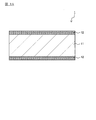
- FIG. 1A is a configuration diagram of a roughened nickel plated plate according to the present embodiment.
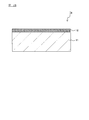
- FIG. 1B is a configuration diagram of a roughened nickel plated plate according to another embodiment.
- FIG. 2 is a schematic diagram (part 1) illustrating an example of a method for manufacturing a roughened nickel-plated plate according to the embodiment.
- FIG. 3 is a schematic diagram (part 2) for explaining an example of the method for manufacturing a roughened nickel-plated plate according to the embodiment.
- FIG. 4 is a schematic diagram (part 3) illustrating an example of a method for manufacturing a roughened nickel-plated plate according to the embodiment.
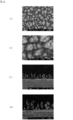
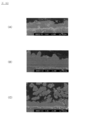
- FIGS. 5A and 5B are images obtained by observing the surface of the roughened nickel-plated plate of Example 28 with a scanning electron microscope (SEM), and FIGS.
- SEM scanning electron microscope
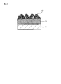
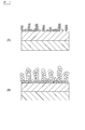
- FIGS. 7A and 7B are schematic views illustrating one embodiment of a roughened nickel layer.
- FIGS. 8A to 8C are schematic views showing one embodiment of a roughened nickel layer.
- FIGS. 9A to 9D are schematic views showing one embodiment of a roughened nickel layer.
- FIGS. 11A to 11C are scanning electron microscope (SEM) cross-sectional photographs of the roughened nickel layer.
- 12 (A) to 12 (C) are scanning electron microscope (SEM) cross-sectional photographs of the roughened nickel layer.
- FIGS. 13A and 13B are scanning electron microscope (SEM) cross-sectional photographs of the roughened nickel layer.
- FIG. 14A and FIG. 14B are scanning electron microscope (SEM) cross-sectional photographs of the roughened nickel layer.
- FIG. 15 is a diagram illustrating a method of determining a boundary between a metal substrate and a base nickel layer and a boundary between a base nickel layer and a roughened nickel layer in Examples and Comparative Examples.
- FIG. 1A is a diagram showing a configuration of a roughened nickel-plated plate 1 of the present embodiment.
- a roughened nickel plating plate 1 of the present embodiment has a roughened nickel layer 12 formed on a metal substrate 11 as an outermost layer.
- the roughened nickel layer 12 has a surface lightness L * of 30 to 50 and an 85 ° glossiness of 3 to 50.
- a roughened nickel plating plate 1 is illustrated in which a roughened nickel layer 12 is formed on both surfaces of a metal base material 11.
- the present invention is not particularly limited to the embodiment.
- a roughened nickel layer 12 may be formed on one surface of the metal substrate 11 as in a roughened nickel plated plate 1a shown in FIG. 1B.
- the metal substrate 11 serving as the substrate of the roughened nickel plating plate 1 of the present embodiment is not particularly limited, but a metal plate or a metal foil made of a kind of pure metal selected from Fe, Cu, Al and Ni, or , Fe, Cu, Al and Ni, a metal plate or a metal foil made of an alloy containing one selected from the group consisting of a steel plate, an iron plate, a stainless steel plate, a copper plate, an aluminum plate, and a nickel plate. May be either a pure metal or an alloy, and may be in the form of a foil.) Among these, plating is easy to perform even with relatively simple pretreatment.
- a steel plate or a copper plate is preferable because a roughened nickel layer having high adhesion to a metal substrate is easily formed, and particularly, a low carbon aluminum killed steel (having a carbon content of 0.01 0.15% by weight), an ultra-low carbon steel having a carbon amount of 0.01% by weight or less (preferably a carbon amount of 0.003% by weight or less), or Ti or Nb added to an ultra-low carbon steel.
- a low carbon aluminum killed steel having a carbon content of 0.01 0.15% by weight
- an ultra-low carbon steel having a carbon amount of 0.01% by weight or less (preferably a carbon amount of 0.003% by weight or less)
- Ti or Nb added to an ultra-low carbon steel.
- Non-ageing ultra-low carbon steel is preferably used.
- a hot-rolled sheet of a metal substrate is pickled to remove scale (oxide film) on the surface, then cold-rolled, and then, a steel sheet, a stainless steel sheet, and a copper sheet which are subjected to electrolytic cleaning of rolling oil.
- An aluminum plate, or a nickel plate can be used as the substrate.
- what performed annealing or temper rolling after electrolytic cleaning may be used. In this case, the annealing may be either continuous annealing or box-type annealing, and is not particularly limited.
- a copper foil, a nickel foil, an iron foil, or the like can be used as a metal substrate as an electrolytic foil produced by an electroforming method or the like.
- a metal substrate having a passivation film formed on its surface such as a stainless steel plate or a nickel plate
- roughened nickel plating or a plating process for forming a base metal plating is performed.
- a strike-nickel plated one it is preferable to use a strike-nickel plated one.
- the conditions for strike nickel plating are not particularly limited, and include, for example, the following conditions. Under the following conditions, the amount of nickel deposited by the strike nickel plating is usually 0.08 to 0.89 g / m 2. However, when the underlying nickel layer is formed, the amount of nickel deposited by the strike nickel plating and the underlying nickel layer Is measured as the nickel adhesion amount of the underlying nickel layer.
- Bath composition nickel sulfate hexahydrate 100-300 g / L, sulfuric acid 10-200 g / L pH: 1.0 or less Bath temperature: 40-70 ° C Current density: 5 to 100 A / dm 2 Plating time: 3-100 seconds
- the thickness of the metal substrate 11 is not particularly limited, but is preferably 0.01 to 2.0 mm, more preferably 0.025 to 1.6 mm, and still more preferably 0.025 to 0.3 mm.
- the roughness of the metal substrate 11 is not particularly limited, but the arithmetic average roughness Ra of the probe-type surface roughness meter is 0.05 to 2.0 ⁇ m, more preferably 0.05 to 0.2 ⁇ m.
- the thickness is 9 ⁇ m, and more preferably 0.05 to 0.5 ⁇ m.
- the roughened nickel layer 12 formed on the outermost surface of the roughened nickel plating plate 1 of the present embodiment has a surface whose brightness L * is controlled to 30 to 50 and 85 ° glossiness is controlled to 3 to 50. It is. According to the present embodiment, by controlling the lightness L * and 85 ° glossiness of the surface of the roughened nickel layer 12 within the above ranges, it is possible to maintain good adhesion of the roughened nickel layer 12 to the metal substrate 11.
- the roughened nickel-plated plate 1 can exhibit excellent adhesion to other members.
- the present inventors have determined the relationship between the lightness L * and 85 ° glossiness of the surface of the roughened nickel layer 12 and the adhesion of the roughened nickel layer 12 to the metal substrate 11 and the adhesion to other members.
- the roughness L * and the 85 ° glossiness of the surface of the roughened nickel layer 12 were set to the above ranges, whereby the roughened nickel plating was performed while maintaining good adhesion of the roughened nickel layer 12.
- the present inventors have found that the plate 1 can exhibit excellent adhesion to other members, and have completed the present invention.
- the adhesion of the roughened nickel layer 12 to the metal substrate 11 attention is also paid to the adhesion of the roughened nickel layer 12 to the metal substrate 11. For the following reasons. That is, even if the roughened nickel layer 12 is formed, the roughened nickel layer 12 can easily fall off from the metal substrate 11 even if excellent adhesion to other members can be exhibited. In this case, since the roughened nickel layer 12 falls off, the effect of forming the roughened nickel layer 12, that is, the effect of exhibiting excellent adhesion to other members, is not achieved. It will be enough. Therefore, according to the present inventors, from such a viewpoint, attention has been paid to the adhesion of the roughened nickel layer 12 to the metal base material 11, and this has been improved.
- the lightness of the surface of the roughened nickel layer 12 is 30 to 50, preferably 30 to 48, more preferably 30 to 45, and even more preferably 35 to 45 in L * value. Further, from the viewpoint of emphasizing production efficiency and production cost, the brightness of the surface of the roughened nickel layer 12 is preferably 36 to 48. If the value of the lightness L * is too small, the adhesion of the roughened nickel layer 12 to the metal substrate 11 will be inferior, while if the value of the lightness L * is too large, the adhesion to other members will be poor. It is inferior to.
- the lightness L * of the surface of the roughened nickel layer 12 can be measured by an SCE method (specular reflection light removal method) using a spectrophotometer in accordance with JIS Z8722.
- the 85 ° glossiness of the surface of the roughened nickel layer 12 is 1.5 to 50, preferably 1.5 to 35, and more preferably 2 to 30. From the viewpoint of emphasizing production efficiency and production cost, the 85 ° glossiness of the surface of the roughened nickel layer 12 is preferably 15 to 50. If the 85 ° glossiness is too small, the adhesion of the roughened nickel layer 12 to the metal substrate 11 will be poor. On the other hand, if the glossiness is too large, the adhesion to other members will be poor.
- the 85 ° glossiness of the surface of the roughened nickel layer 12 can be determined by measuring the 85 ° specular gloss using a gloss meter according to JIS Z8741.
- the 60 ° glossiness of the roughened nickel layer 12 formed on the outermost surface of the roughened nickel plating plate 1 of this embodiment is usually 10 or less.
- the chromaticities a * and b * of the surface of the roughened nickel layer 12 are not particularly limited, it is possible to further improve the adhesion of the roughened nickel layer 12 to the metal substrate 11 and the adhesion to other members. From the viewpoint of being able to do so, the chromaticity a * is preferably 0.1 to 3.0, more preferably 0.3 to 1.5, and the chromaticity b * is preferably 1.0 to 8.0. More preferably, it is 2.0 to 7.0.
- the roughened nickel layer 12 may have the surface lightness L * and 85 ° glossiness within the above ranges, but preferably have an arithmetic average roughness Ra of 0.1 to 3 ⁇ m. 12, from the viewpoint of further improving the adhesion to other members, the arithmetic average roughness Ra is more preferably 0.18 ⁇ m or more, still more preferably 0.3 ⁇ m or more, and From the viewpoint of further improving the adhesion (plating adhesion) of the roughened nickel layer 12, the arithmetic average roughness Ra is more preferably 1.8 ⁇ m or less, still more preferably 1.6 ⁇ m or less, and even more. Preferably it is 1.3 ⁇ m or less.
- the arithmetic average roughness Ra is preferably 0.18 to 0.5 ⁇ m, and more preferably 0.18 to 0.49 ⁇ m.
- the roughened nickel layer 12 preferably has a ten-point average roughness Rz jis of 2.0 to 20.0 ⁇ m, from the viewpoint of further improving the adhesion of the roughened nickel layer 12 to other members.
- the ten-point average roughness Rz jis is more preferably 3 ⁇ m or more, still more preferably 4 ⁇ m or more, and still more preferably 5 ⁇ m or more, and the adhesion of the roughened nickel layer 12 to the metal substrate 11.
- the ten-point average roughness Rz jis is more preferably 16 ⁇ m or less, further preferably 14 ⁇ m or less, and still more preferably 12 ⁇ m or less. Further, from the viewpoint of emphasizing production efficiency and production cost, the ten-point average roughness Rz nis is preferably 3.0 to 7.0 ⁇ m.
- the maximum height roughness Rz of the roughened nickel layer 12 is not particularly limited, but is preferably 2.5 to 25.0 ⁇ m, more preferably 2.5 to 20.0 ⁇ m, and still more preferably 3.5 to 18 ⁇ m. 0.0 ⁇ m.
- the surface roughness Ra, Rzjis, Rz is preferably measured by a laser microscope.
- the adhesion amount of the roughened nickel layer 12 in the roughened nickel plating plate 1 of the present embodiment is not particularly limited, but is preferably 1.34 to 45.0 g / m 2 , and the adhesion of the roughened nickel layer 12 from the viewpoint of further improving the (coating adhesion), the adhesion amount of the roughened nickel layer 12 is more preferably 2.67 g / m 2 or more, more preferably 5 g / m 2 or more, roughening From the viewpoint of further improving the adhesion of the nickel layer 12 to other members, the amount of the roughened nickel layer 12 is preferably 38.0 g / m 2 or less, more preferably 32.0 g / m 2 or less.
- the adhesion amount of the roughened nickel layer 12 can be determined by measuring the total nickel amount of the roughened nickel plating plate 1 using a fluorescent X-ray device. When a base metal plating layer 13 made of nickel, which will be described later, is formed, the total nickel content of the roughened nickel plating plate 1 is measured using a fluorescent X-ray apparatus, and then the total nickel content is measured. It can be obtained by subtracting the amount of nickel corresponding to the metal plating layer 13.
- the amount of nickel corresponding to the base metal plating layer 13 is determined by, for example, cutting the roughened nickel plating plate 1 and observing the cross section with a scanning electron microscope (SEM) to measure the thickness of the base metal plating layer 13.
- SEM scanning electron microscope
- the method for setting the lightness L * and the 85 ° glossiness of the surface of the roughened nickel layer 12 to the above ranges is not particularly limited, but a method of forming the roughened nickel layer 12 by the method described below. And the like.
- the metal substrate 11 is required
- the underlying metal plating layer 13 is formed according to the conditions.
- the roughened nickel layer 12 may be formed directly on the metal base material 11 without forming the base metal plating layer 13.
- the nickel particulate matter 121 is precipitated on the metal base material 11 in an aggregated state.
- a coated nickel plating is further applied to cover the nickel particles 121 with a nickel coating 122, thereby forming a base metal plating layer formed on the metal base 11 as necessary. 13, the roughened nickel layer 12 is formed.
- the conditions of the roughened nickel plating for precipitating the nickel particulates 121 in an agglomerated state are not particularly limited, but the brightness L * and the 85 ° glossiness of the surface of the roughened nickel layer 12 are suitably controlled in the above ranges. From the viewpoint of being able to do so, a method by electrolytic plating using a plating bath containing nickel sulfate hexahydrate at a concentration of 10 to 100 g / L and ammonium sulfate at a concentration of 1 to 100 g / L is preferable.
- the concentration of nickel sulfate hexahydrate in the plating bath used is preferably 10 to 70 g / L, more preferably 10 to 50 g / L, and still more preferably 15 to 25 g / L.
- nickel chloride hexahydrate may be used as a nickel ion supply source, or nickel chloride hexahydrate and nickel sulfate hexahydrate may be used in combination.
- the concentration of nickel chloride hexahydrate is preferably 1 to 40 g / L.
- the concentration of ammonium sulfate in the plating bath used is preferably 10 to 50 g / L, more preferably 10 to 45 g / L, and further preferably 15 to 40 g. / L.
- the ammonia may be added to the nickel plating bath by adding aqueous ammonia or a salt such as ammonium sulfate or ammonium chloride.
- the concentration of the ammonia in the plating bath is preferably from 0.3 to 0.3.
- the amount is 30 g / L, more preferably 1 to 20 g / L, still more preferably 3 to 15 g / L, and particularly preferably 3 to 12 g / L or less.
- the pH of the nickel plating bath at the time of performing the roughened nickel plating for precipitating the nickel particulate matter 121 in an agglomerated state is more suitable for the lightness L * and the 85 ° glossiness of the surface of the roughened nickel layer 12. It is preferably 4.0 to 8.0 from the viewpoint of controllability. If the pH is too high, nickel ions in the bath easily form hydrates and cause poor plating, so the upper limit is more preferably 7.5 or less, and even more preferably 7.0 or less. If the pH is low, the bath resistance becomes low, and it is difficult for nickel particles to precipitate in a state where secondary particles are formed, and it is likely to become a normal deposition form (flat plating), so that a roughened nickel layer is formed. Because it is difficult to perform, it is more preferably 4.5 or more, further preferably 4.8 or more, and particularly preferably 5.0 or more.
- the current density at the time of performing the roughening nickel plating for precipitating the nickel particulates 121 in an aggregated state is from the viewpoint that the brightness L * and the 85 ° glossiness of the surface of the roughened nickel layer 12 can be more appropriately controlled. , Preferably 5 to 40 A / dm 2 . If the current density is high, the deposition efficiency tends to decrease, and plating unevenness and surface roughness control unevenness are likely to occur in the plating process range. In particular, in order to secure a large area of 100 cm 2 or more, 30 A / dm 2 or less Is more preferably 25 A / dm 2 or less, and particularly preferably 20 A / dm 2 or less.
- the current density is determined by the nickel ion concentration in the nickel plating bath (Example described later). Is controlled by nickel sulfate hexahydrate (g / L) in plating bath), temperature of nickel plating bath, pH of nickel plating bath, ammonia concentration in nickel plating bath, halogen atom concentration in nickel plating bath, etc. It is preferable to perform control accordingly.
- the bath temperature of the nickel plating bath at the time of performing the roughened nickel plating is not particularly limited. However, from the viewpoint that the brightness L * and the 85 ° glossiness of the surface of the roughened nickel layer 12 can be more suitably controlled, it is preferable.
- the temperature is 25 to 60 ° C, more preferably 25 to 50 ° C, and still more preferably 30 to 50 ° C.
- the method of stirring is not particularly limited, and examples thereof include bubbling and pump circulation.
- the type of gas is not particularly limited, but it is preferable to use air as a gas from the viewpoint of versatility, and the timing of supplying the gas is preferably continuous ventilation for stable stirring. .
- stirring is too strong, it is difficult to obtain the desired roughened shape if the stirring is too strong. Therefore, for example, 1 L / min or less is preferable for a plating solution having a volume of 2 L.
- continuous circulation is preferable for stably stirring.
- the amount of precipitation when the nickel particulates 121 are precipitated in an agglomerated state by the roughened nickel plating is not particularly limited, but the brightness L * and 85 ° glossiness of the surface of the roughened nickel layer 12 are controlled in the above ranges. From the viewpoint of improving the surface roughness, it is preferably 0.89 to 4.45 g / m 2 , and from the viewpoint of further improving the adhesion of the roughened nickel layer 12 to other members, the nickel particulates 121 are aggregated.
- the precipitation amount for deposition and a state is more preferably 1.34 g / m 2 or more, more preferably at 1.60 g / m 2 or more, with respect to the metal substrate 11, adhesion of the roughened nickel layer 12
- the precipitation amount when the nickel particulate matter 121 is precipitated in an aggregated state is more preferably 4.01 g / m 2 or less. And more preferably 3.56 g / m 2 or less, and particularly preferably 3.12 g / m 2 or less.
- the amount of precipitation when the nickel particulate matter 121 is precipitated in an aggregated state is preferably 1.34 to 2.23 g / m 2 .
- the nickel particulates 121 are coated with the nickel coating 122.
- the coated nickel plating for covering the nickel particulates 121 with the nickel coating 122 may be performed by any plating method of electrolytic plating or electroless plating, but is preferably formed by electrolytic plating.
- the coated nickel plating is performed by the electrolytic plating method, for example, nickel plating hexahydrate 200 to 350 g / L, nickel chloride hexahydrate 20 to 60 g / L, and boric acid 10 to 50 g / L as a nickel plating bath.
- a Watt bath having a bath composition of pH 3.0 to 5.0, a bath temperature of 40 to 70 ° C., and a current density of 5 to 30 A / dm 2 (preferably 10 to 20 A / dm 2 ), followed by nickel plating. Thereafter, a method of washing with water can be used.
- the amount of deposition (coating amount) when the nickel particulate matter 121 is coated with the nickel coating 122 by the coated nickel plating is not particularly limited, but the lightness L * and 85 ° glossiness of the surface of the roughened nickel layer 12 are set as described above. From the viewpoint of controlling within the range, it is preferably 4.45 to 26.70 g / m 2 , and from the viewpoint of further improving the adhesion (plating adhesion) of the roughened nickel layer 12, the nickel particles 121 are preferably used.
- the deposition amount (coating amount) when coating with the nickel coating 122 is more preferably 6.23 g / m 2 or more, and from the viewpoint of further improving the adhesion of the roughened nickel layer 12 to other members.
- the amount of precipitation when the nickel particulate matter 121 is coated with the nickel coating 122 is preferably 4.45 to 8.90 g / m 2 .
- the ratio between the amount of precipitation by the roughened nickel plating and the amount of deposition by the coated nickel plating is not particularly limited, but is preferably a weight ratio of “the amount of deposition by the roughened nickel plating: the amount of deposition by the coated nickel plating”.
- the ratio is 1: 2 to 1:14, more preferably 2: 4.5 to 2:15, and still more preferably 2: 5 to 2:15.
- a nickel base layer is formed as the base metal plating layer 13
- a part of the base nickel plating This also contributes to the growth of the layer (thickening of the portion where the base is exposed without nickel particles). Therefore, in this case, the deposition amount is the sum of the coating amount of the nickel coating 122 by the coating nickel plating and the formation amount of the base nickel layer by the coating nickel plating.
- the base metal plating layer 13 is formed between the metal base 11 and the roughened nickel layer 12. It is preferably formed, and the underlying metal plating layer 13 is preferably a nickel plating layer or a copper plating layer, and more preferably a nickel plating layer.
- the nickel particulates 121 formed by the above-described roughened nickel plating are in a state in which the particulate precipitates are aggregated and precipitated in a protruding state to form an aggregate, and a viewpoint of adhesion to other members is obtained.
- a gap is provided between the respective aggregates, so that the entire surface of the metal substrate 11 may not be completely covered. Therefore, for example, when a steel sheet is used as the metal base material 11, it is preferable to provide the base metal plating layer 13 in order to improve the effect of suppressing the generation of rust on the steel sheet. In addition, for the purpose of such an effect of improving corrosion resistance, it is preferable to select the metal base material 11 according to the application and perform a base plating process according to the selection. When using a steel plate or copper for the metal base material 11, It is preferable to provide a base nickel plating layer or a base copper plating layer as the base metal plating layer 13.
- the compatibility with the subsequent coating plating is good, and the plating adhesion of the roughened nickel layer 12 can be further improved.
- the plating adhesion effect can be obtained only by the coating nickel plating treatment without the base metal plating layer 13, nickel tends to preferentially precipitate on the nickel particles 121 in the coating nickel plating treatment. From such a viewpoint, it is more preferable to form the base metal plating layer 13 in order to improve the corrosion resistance.
- the plating adhesion of the roughened nickel layer 12 can be further improved by performing an acid treatment or the like in the pretreatment.
- the base metal plating layer 13 can be formed by plating the metal base 11 in advance before forming the roughened nickel layer 12 on the metal base 11.
- the base metal plating layer 13 is a nickel plating layer, it may be formed by using any plating method of electrolytic plating or electroless plating, but is preferably formed by electrolytic plating.
- the base metal plating layer 13 is a nickel plating layer and an electrolytic plating method is used to form the base nickel plating layer, for example, nickel sulfate hexahydrate 200 to 350 g / L, nickel chloride hexahydrate 20 to 60 g / L, boric acid 10 to 50 g / L using a watt bath, pH 3.0 to 5.0, bath temperature 40 to 70 ° C, current density 5 to 30 A / A method of performing nickel plating under the condition of dm 2 (preferably 10 to 20 A / dm 2 ) and then washing with water can be used.
- nickel sulfate hexahydrate 200 to 350 g / L nickel chloride hexahydrate 20 to 60 g / L
- boric acid 10 to 50 g / L using a watt bath, pH 3.0 to 5.0, bath temperature 40 to 70 ° C, current density 5 to 30 A /
- dm 2 preferably 10 to 20 A / dm 2
- the amount of the roughened nickel layer 12 in the roughened nickel plating plate 1 of the present embodiment when the base metal plating layer 13 is formed is such that the adhesion between the metal substrate 11 and the roughened nickel layer 12 is further improved. From the viewpoint of performing the treatment, it is preferably 26.70 g / m 2 or less, more preferably 4.45 to 22.25 g / m 2 , still more preferably 4.45 to 17.80 g / m 2 , and particularly preferably 4. 45 to 13.35 g / m 2 .
- the total adhesion amount of the roughened nickel layer 12 and the base metal plating layer 13 in the roughened nickel plating plate 1 of the present embodiment is not particularly limited. From the viewpoint that the adhesion of the roughened nickel layer 12 to the substrate 11 and the adhesion to other members can be further improved, it is preferably 5.0 to 50.00 g / m 2 , more preferably It is 12.02 to 50.00 g / m 2 , more preferably 12.28 to 40.94 g / m 2 , and particularly preferably 12.28 to 32.49 g / m 2 .
- the total adhesion amount of the roughened nickel layer 12 and the underlying metal plating layer 13 is preferably 10.24 to 22.25 g / m 2 . Further, when high corrosion resistance is required, and particularly when the adhesion of the roughened nickel layer 12 to the metal substrate 11 and the adhesion to other members are required, the roughened nickel layer 12 and the underlying metal plating are required.
- the total adhesion amount with the layer 13 is preferably 32.50 to 57.85 g / m 2 .
- the total adhesion amount of the roughened nickel layer 12 and the base metal plating layer 13 can be determined by measuring the total nickel amount of the roughened nickel plating plate 1 using a fluorescent X-ray device.
- nickel particles 121 are precipitated on the metal substrate 11 in an agglomerated state by roughening nickel plating.
- a method of coating the nickel particulates 121 with the nickel coating 122 by further applying a coating nickel plating is adopted, and by controlling these forming conditions, the brightness L * of the surface of the roughened nickel layer 12 and The 85 ° glossiness can be set in the above range.
- Rz jis is a parameter indicating the height difference of the surface, but simply parameters such as Ra and Rz indicating Rz jis or other roughness indicate the adhesion to other members and the roughness of the nickel layer 12. It was found that the adhesion could not be controlled. In other words, the tendency is that a certain level of height difference (Rz jis ) can ensure the adhesion to other members, while if the height difference (Rz jis ) is too large, the metal substrate 11 may be roughened. There is a tendency that the adhesion of the nickel layer 12 tends to deteriorate. However, in particular, it has been found that the adhesion of the roughened nickel layer 12 to the metal substrate 11 is not simply determined by Rz nis alone.
- the density of the protruding aggregates in the roughened nickel layer 12 if the density of the protruding aggregates is too high, resin or the like cannot enter between the protruding shapes, and the adhesion to other members such as a resin film may occur. It turned out that the nature could not be secured. On the other hand, if the density of the protruding aggregates is too low, each protruding aggregate is likely to be thin and easily broken, and the adhesion of the roughened nickel layer 12 to the metal substrate 11 may be reduced. It was found that the anchor effect was not obtained due to the presence of the protrusions or the amount of the projection-like aggregate itself was too small, and the adhesion to other members such as a resin film was not obtained.
- the numerical value of the lightness L * fluctuates due to the unevenness of the plate surface, but a projection-like aggregate composed of secondary particles (nickel particulates 121) as shown in FIG.
- the present inventors have found that the influence of not only the size (Rz jis ) of the protrusions but also the particle size of the primary particles of the plating particles at the tips of the protrusions is large. That is, the inventors have found that the lightness L * fluctuates when the surface shape of the tip of the protruding aggregate changes depending on the size of the primary particles. Furthermore, even if the lightness L * is in a suitable range, the problem that the adhesion of the roughened nickel layer 12 to the metal base material 11 may be poor may be found.
- the lightness L * is in a suitable range, while the plating particles are large and porous. It is considered that the plating particles are easily peeled off from the metal substrate 11.
- Rz jis is likely to be high, so that the protruding aggregates are easily broken and fall off.
- the measurement of plating particles is very troublesome, when such plating particles are large, the glossiness measured at a low angle of incident light on the plating plate of 85 ° glossiness is extremely low. It was also found out.
- the present inventors have conceived the roughened nickel plated plate 1 in which the lightness L * and the 85 ° glossiness of the roughened nickel layer 12 are in the above-mentioned specific ranges based on such knowledge.
- the plating layer having such a projection-like aggregate has a plating current, under the condition that energization is performed under a situation where the supply of nickel ions is insufficient. It can be formed by plating. That is, it can be formed by insufficient supply of nickel ions to the plating current to cause abnormal electrodeposition.
- the present inventors have solved the problem of simultaneously satisfying both the adhesion of the roughened nickel layer 12 to the metal base material 11 and the adhesion to other members. Has found that the size of the primary particles, the size of the protruding aggregate, and the shape of the protruding aggregate that constitute the roughened nickel layer 12 are important.
- FIG. 7B is a diagram showing a specific mode of the roughened nickel layer 12 according to the present embodiment
- FIG. 7D shows the roughened nickel layer 12 shown in FIG. It is a schematic diagram based on a SEM photograph.
- FIG. 7A is a diagram showing an embodiment of a plating layer obtained by roughening nickel plating, and is a schematic diagram based on the SEM photograph shown in FIG. 14B.
- the mode as shown in FIG. 7B is obtained by forming a plating layer of the mode as shown in FIG. 7A by roughening nickel plating, and then subjecting it to coating nickel plating. .
- FIG. 7A and 7B illustrate the case where the underlying nickel plating layer is formed
- the present invention is not particularly limited to the mode of forming the underlying nickel plating layer (FIG. 8).
- FIG. 8 The same applies to (A) to FIG. 8 (C), FIG. 9 (A) to FIG. 9 (D), and FIG. 10 (A) to FIG. 10 (D).)
- (1) primary particles forming a protruding aggregate are: Have an appropriate size without being too small (the average particle size of the primary particles is preferably from 0.3 to 3.0 ⁇ m, more preferably from 0.5 to 2.0 ⁇ m);
- the shape of the aggregate composed of the secondary particles in which the primary particles are aggregated is a projection or a column, and (3) the height of the aggregate is neither too low nor too high (the height is preferably 1 to 20 ⁇ m, more preferably 2 to 15 ⁇ m, and particularly preferably 2.0 to 10.0 ⁇ m from the viewpoint of emphasizing production efficiency and production cost), (4) the existence of the aggregate Density is not too sparse (somewhat The above-mentioned problem is solved by satisfying the conditions (1) to (4) of (protruding aggregates are formed at a distance of not too close and not too far apart).
- the primary particles are too small, the adhesion (coupling) between the primary particles becomes poor, and the plating adhesion decreases. If the primary particles are too large, the projection or columnar shape cannot be obtained, or the projections locally grow excessively, and the projections are easily broken by external force or the like, and as a result, the plating adhesion is poor.
- the fact that the layer has an appropriate size without being too small is, more specifically, as also confirmed in the cross-sectional SEM images of the roughened nickel layer 12 shown in FIGS. 5C and 5D.
- 70% or more of the primary particles constituting the projecting or columnar secondary particles are composed of primary particles having a particle size of 0.3 to 3.0 ⁇ m, more preferably 0.5% or more.
- 70% of the whole means that 70% or more of the cross-sectional area of all the primary particles is the area of the particles having the particle size range.
- it is difficult to derive each particle size from the cross-sectional SEM image but if the particle size of the primary particles constituting the secondary particles is too small, the particle size is clearly smaller than 0.3 ⁇ m. Is 70% or more, so that clear identification is possible.
- the lightness L * and the 85 ° glossiness fall within the predetermined ranges of the present invention, and the adhesion of the roughened nickel layer 12 to the metal substrate 11 is improved. And at the same time, the adhesiveness to other members.
- the primary particle is very fine or the height of the protruding aggregate is low, so that the lightness L * is within the predetermined range of the present invention. Therefore, the adhesiveness of the roughened nickel layer 12 to the metal base material 11 or the adhesiveness to other members is inferior.
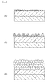
- the embodiment shown in FIG. 7A is an embodiment corresponding to Comparative Examples 11 to 16 and 34 described later.
- the height of the projection-like aggregate is low or the projection-like aggregate itself is not formed, and the lightness L * falls outside the predetermined range of the present invention, and the roughness of the metal substrate 11 is reduced.
- the adhesion of the nickel layer 12 or the adhesion to other members is inferior.
- the mode shown in FIG. 8A corresponds to Comparative Examples 17 to 20 described later, and the mode shown in FIGS. 8B and 8C corresponds to Comparative Examples 1 to 4 described later. 33, 37 to 39.
- the height of the projection-like aggregate is too high.
- the formation density of the protruding aggregates is also low, and the lightness L * falls outside the predetermined range of the present invention, resulting in poor adhesion of the roughened nickel layer 12 to the metal substrate 11.
- the mode shown in FIG. 10A corresponds to Comparative Examples 21 to 23, 25 to 29, 35, and 36 described below, and the mode shown in FIG. 10B corresponds to Comparative Example 5 to be described later. This is a corresponding aspect.
- the height of the protruding aggregate is too high.
- the lightness L * and the 85 ° glossiness are out of the predetermined ranges of the present invention, and the adhesion of the roughened nickel layer 12 to the metal substrate 11 is inferior.
- the embodiment shown in FIG. 10C is an embodiment corresponding to Comparative Example 32 described later
- the embodiment shown in FIG. 10D is an embodiment corresponding to Comparative Examples 6 and 7 described later.
- FIGS. 7 (A), 8 (A) to 8 (C), FIGS. 9 (A) to 9 (D), and FIGS. 10 (A) to 10 In the embodiment shown in D), one of the lightness L * and the 85 ° glossiness falls outside the predetermined range of the present invention, and the adhesion of the roughened nickel layer 12 to the metal base material 11 and the adhesion to other members.
- the brightness L * and 85 ° gloss fall within the predetermined ranges of the present invention, It has been found that both the adhesion of the roughened nickel layer 12 to the material 11 and the adhesion to other members can be satisfied at the same time.
- the above-mentioned method can be mentioned.
- a precipitation step and a growth step described below are performed.
- the roughened nickel layer 12 as shown in FIG. 7B is formed. That is, first, as described above, as roughened nickel plating, a suitable current for exciting precipitation is applied (applied voltage) to a diluted nickel aqueous solution to deposit metal nickel from many nuclei simultaneously. And the growth of precipitated particles in the plane direction can be suppressed to some extent. Also, at this time, the nuclei of the primary particles are likely to precipitate preferentially on the projections formed by the precipitated particles.
- the shape of the secondary particles can be a projection. However, even if such an aggregate is formed, if the primary particles are too small as shown in FIG. 7A, the contact surface between the primary particles is too small, so that the primary particles are easily peeled. . Therefore, as described above, the coated nickel plating is performed after the roughened nickel plating. Here, it is described as "coating”, but according to studies by the present inventors, according to such coated nickel plating, it is possible to cover the primary particles formed by roughened nickel plating. It has been confirmed that, in addition to precipitation, grain growth in which primary particles grow actually occurs.
- the primary particles by the coated nickel plating is expressed not only on the top surface of the protruding aggregate, but also on the particles on the side surface of the aggregate and the particles inside the aggregate.
- the primary particles have an appropriate size, whereby the adhesion between the primary particles is improved, and the thickness of the protruding aggregate is increased, so that the primary particles are hardly broken. Therefore, the roughened nickel layer 12, which is an embodiment shown in FIG. 7B, has good adhesion of the roughened nickel layer 12 to the metal substrate 11. Further, in addition to this, since it has a protruding assembly having a moderate height, the adhesiveness to other members is also excellent.
- the present embodiment as a method of forming the roughened nickel layer as shown in FIG. 7B, a method of performing coated nickel plating after roughened nickel plating is described. If the conditions (1) to (4) are satisfied, the brightness L * and the 85 ° glossiness naturally fall within the predetermined ranges of the present invention, and the adhesion of the roughened nickel layer 12 to the metal substrate 11 and other members Thus, a roughened nickel-plated sheet having excellent adhesion to the substrate can be obtained, so that the step of coating nickel may be omitted.
- FIG. 11A shows a cross-sectional SEM photograph of the roughened nickel layer according to the embodiment shown in FIG. 8A
- FIG. 11A shows a cross-sectional SEM photograph of the roughened nickel layer according to the embodiment shown in FIG.
- FIG. 11 (B) is a cross-sectional SEM photograph of the roughened nickel layer according to the embodiment shown in FIG. 8 (C)
- FIG. 11 (C) is a cross-sectional SEM photograph of the roughened nickel layer according to the embodiment shown in FIG. 9 (A).
- FIG. 12A shows a cross-sectional SEM photograph of the roughened nickel layer according to the embodiment shown in FIG. 9B
- FIG. 12B shows the roughened nickel layer according to the embodiment shown in FIG. 9D.
- FIG. 9D shows a cross-sectional SEM photograph of the roughened nickel layer according to the embodiment shown in FIG. 9D.
- FIG. 12 (C) shows a cross-sectional SEM photograph of the layer
- FIG. 13 (A) shows a cross-sectional SEM photograph of the roughened nickel layer according to the embodiment shown in FIG. 10 (A).
- FIG. 13B shows a cross-sectional SEM photograph of the roughened nickel layer.
- the adhesion of the roughened nickel layer 12 to the metal base 11 is good, and the adhesion to other members is excellent. Therefore, it is used by being joined to other members, for example, various containers that require adhesion to various members such as resins and active materials, electronic device members (substrates, etc.), battery members (outer tanks, collectors, etc.). (Electric conductor, tab lead).
- the roughened nickel-plated plate 1 of the present embodiment is excellent in the adhesion of the roughened nickel layer 12, that is, the adhesion to the substrate 11, even if the plated plates overlap or come into contact with each other, for example. Since the roughened nickel layer 12 on the surface is unlikely to peel off or fall off, it can be suitably used as the roughened nickel plating plate 1 having the roughened nickel layer 12 on the outermost surfaces on both sides as shown in FIG. 1A.
- the roughened nickel layer 12 is formed only on one side as in the roughened nickel plated plate 1 shown in FIG. 1B. I just need.
- the surface on which the roughened nickel layer 12 is not formed is such that the substrate 11 is located on the outermost surface.
- the substrate 11 when the substrate 11 is a steel plate, it may be an untreated steel plate, Alternatively, a surface treatment according to required characteristics such as nickel plating, zinc plating, and chemical conversion treatment may be performed.
- the surface on which the roughened nickel layer 12 is not formed is formed on a normal nickel plating layer (for example, a nickel plating layer formed under the conditions for forming the above-described base nickel plating layer).
- a normal nickel plating layer for example, a nickel plating layer formed under the conditions for forming the above-described base nickel plating layer.
- both surfaces of the base material 11 are covered with the nickel layer, which is preferably applicable.
- the roughened nickel plating plate 1 as shown in FIG. 1B is manufactured, for example, in the step of applying the roughened nickel plating, the plating process is performed without supplying electricity to the surface on which the roughened nickel layer 12 is not formed.
- a roughened nickel-plated steel sheet having a roughened nickel layer 12 on only one side can be obtained by a method of performing the masking method.
- ⁇ Surface roughness> Using a laser microscope (manufactured by Olympus, model number: OLS3500) on the surface of the roughened nickel plated plate where the roughened nickel layer is formed, in accordance with JIS B0601: 2013, 97 ⁇ m ⁇ 129 ⁇ m (length ⁇ width) After scanning a visual field having a measurement visual field width of 129 ⁇ m and a measurement area of about 12,500 ⁇ m 2 (12,500 ⁇ 100)), use analysis software (software name: LEXT-OLS) in an analysis mode: under the conditions of roughness analysis. By the analysis, the arithmetic average roughness Ra and the ten-point average roughness Rz jis were measured. The cut-off value when measuring with a laser microscope was a wavelength of about 43 ⁇ m (43.2 on the display), which is ⁇ of the measurement visual field width (129 ⁇ m).
- the measurement is performed using a fluorescent X-ray apparatus after each step of forming the underlying nickel layer, the nickel granules, and the nickel coating, and thereby the under nickel layer, the roughened nickel layer (the nickel particulates and the nickel coating) are measured.
- the nickel content was determined. Specifically, once the underlayer nickel layer was formed, the amount of nickel in the underlayer nickel layer was determined once using a fluorescent X-ray apparatus. Then, after forming the nickel granules, the total nickel amount was determined again by the fluorescent X-ray apparatus, and the difference between the obtained total nickel amount and the nickel amount of the underlying nickel layer was defined as the nickel amount of the nickel granules.
- the total nickel amount is again obtained by the fluorescent X-ray apparatus, and the difference between the total nickel amount before the nickel film formation and the total nickel amount after the formation is obtained, thereby similarly obtaining the nickel amount of the nickel film.
- the total nickel amount of the nickel particles and the nickel coating was determined as the amount of the roughened nickel layer deposited.
- the nickel amount of each layer cannot be measured by the above-described fluorescent X-ray apparatus.
- the base material that does not contain nickel such as a steel plate in advance, under a plating condition in which a predetermined amount of nickel of the underlying nickel layer is obtained, the base material is formed into a stainless steel plate, and a nickel-containing metal plate such as a nickel plate.
- the nickel amount was measured by the above-described method.
- the measurement of the nickel amount is not limited to such a method, and the following method may be used. In the present embodiment, the following method was partially adopted.
- a roughened nickel-plated plate on which an underlying nickel layer, nickel granules, and a nickel film are formed is measured by a fluorescent X-ray apparatus to obtain the total nickel amount of the layer formed on the roughened nickel-plated plate. Ask for.
- the roughened nickel-plated plate is cut, and the cross section is observed with a scanning electron microscope (SEM) to measure the thickness of the underlying nickel layer, to determine the amount of nickel converted from the thickness of the underlying nickel layer, This is defined as the nickel content of the underlying nickel layer.
- SEM scanning electron microscope
- the total nickel content of the nickel particulate matter and the nickel coating can be obtained, and this can be used as the adhesion amount of the roughened nickel layer.
- the roughened nickel layer 12 is formed as the nickel coating 122 that covers the nickel granules 121, and a part of the roughened nickel layer 12 is to be formed with the base nickel layer. According to such a method, it is possible to obtain the nickel amount of the base nickel layer in consideration of the growth (thickening) of the base nickel layer by coating nickel plating.
- FIG. 15 is a diagram for explaining a method of determining the boundary between the metal base and the underlying nickel layer and the boundary between the underlying nickel layer and the roughened nickel layer in the examples and comparative examples.
- A) and FIG. 15B show the same scanning electron microscope (SEM) photograph side by side. In FIG. 15, each boundary position is shown by a broken line in FIG. 15B. .
- an adhesive tape (trade name “Cellotape (registered trademark)”, manufactured by Nichiban Co., Ltd.) was applied to the surface of the roughened nickel plated plate obtained in each of the examples and the comparative examples, on which the roughened nickel layer was formed, with a width of 24 mm. After sticking so as to have a length of 50 mm, a peeling test was carried out with the attached adhesive tape in the manner of a peeling test method described in JIS H8504. Then, the pressure-sensitive adhesive tape after the peeling test was affixed to the same backing as the reference sample, and the lightness L * , chromaticity a * , and b * were measured in the same manner as above using a spectrophotometer.
- T-peel strength of polypropylene resin (PP resin)>
- the roughened nickel-plated plates obtained in the examples and comparative examples were cut to produce two test plates having a width of 15 mm and a length of 50 mm, which were used as T-peel test pieces. Then, each of the two T-peel test pieces was bent at an angle of 90 ° at a position of 20 mm in length.
- the bonding surface to be evaluated is a bonding surface between a polypropylene resin and a T-peel test piece, and the product name “Modic” is an adhesive layer for stabilizing the test), and the temperature is 190 ° C., the pressing time is 5 seconds, the heat Heat sealing was performed under the conditions of a sealing pressure of 2.0 kgf / cm 2 , and two T-peel test pieces were joined via a polypropylene resin film.
- the position where the polypropylene resin film is sandwiched is the end in the length direction of the T-peel test body, and the entire polypropylene resin film becomes the bonding surface.
- the T-peel test body thus produced was subjected to a tensile test using a tensile tester (a universal material tester, Tensilon RTC-1350A manufactured by ORIENTEC), and the peeling load (T-peel strength) was measured. Measurement conditions were room temperature and a tensile speed of 10 mm / min. It can be determined that the higher the T-peel strength, the better the adhesion to the resin.
- Example 1 As a substrate, a steel sheet obtained by annealing a cold-rolled low-carbon aluminum-killed steel sheet (thickness: 0.25 mm) was prepared.
- the prepared steel sheet is subjected to alkaline electrolytic degreasing, pickling of sulfuric acid immersion, and then electroplating under the following conditions using a base nickel plating bath having the following bath composition, and the base nickel plating on both sides of the steel sheet, respectively.
- a layer was formed.
- Bath composition nickel sulfate hexahydrate 250 g / L, nickel chloride hexahydrate 45 g / L, boric acid 30 g / L pH: 4.2 Bath temperature: 60 ° C Current density: 10 A / dm 2 Plating time: 30 seconds
- the steel sheet on which the base nickel layer is formed is subjected to electrolytic plating (roughened nickel plating) under the following conditions using a roughened nickel plating bath having the following bath composition, whereby the steel sheet on both sides of the steel sheet is formed.
- Nickel particulate matter was deposited on the nickel layer.
- Bath composition Nickel sulfate hexahydrate 20 g / L, ammonia sulfate 20 g / L pH: 6.2
- the steel sheet on which the nickel particulate matter is deposited on the base nickel layer is subjected to electrolytic plating (coated nickel plating) under the following conditions using a coated nickel plating bath having the following bath composition.
- the roughened nickel-plated plate of Example 1 was obtained by coating the nickel particles deposited on the nickel layer with a nickel film.
- Examples 2 to 15 The plating bath and the plating conditions of the roughened nickel plating were changed to the conditions shown in Table 1, and the processing time of the coated nickel plating was changed so that the amount of nickel film formed was as shown in Table 1. Except for the above, roughened nickel-plated plates of Examples 2 to 15 were obtained and evaluated in the same manner as in Example 1. Table 1 shows the results.
- Examples 16 to 31 Except that the conditions of the roughened nickel plating were changed to the conditions shown in Table 2, and the processing time of the coated nickel plating was changed so that the amount of nickel film formed was as shown in Table 2, In the same manner as in Example 1, the roughened nickel-plated plates of Examples 16 to 31 were obtained and evaluated in the same manner. Table 2 shows the results.
- Example 32 As a metal substrate, a copper plate (electrolytic copper foil manufactured by Fukuda Metal Foil & Powder Co., Ltd. (as measured by a laser microscope: Ra: 0.1 ⁇ m, Rz jis : 1.7 ⁇ m)) was used.
- Example 2 was carried out in the same manner as in Example 1 except that the conditions were changed to the conditions shown in Table 1 and that the treatment time of the coated nickel plating was changed so that the amount of the deposited nickel film became the amount shown in Table 2.
- a roughened nickel-plated plate of No. 32 was obtained and evaluated in the same manner, and the results are shown in Table 2.
- Examples 33 to 36 Except that the conditions of the roughened nickel plating were changed to the conditions shown in Table 2, and the processing time of the coated nickel plating was changed so that the amount of nickel film formed was as shown in Table 2, In the same manner as in Example 1, the roughened nickel-plated plates of Examples 33 to 36 were obtained and evaluated in the same manner. Table 2 shows the results.
- Examples 37 to 41 >> SUS304 (Example 37), SUS316 (Example 38), SUS430 (Example 39), SUS444 (Example 40), and a pure nickel plate (Example 41) were used as the metal base, and roughened nickel was used.
- Example 1 was the same as Example 1 except that the plating conditions were changed to the conditions shown in Table 2 and the treatment time of the coated nickel plating was changed so that the amount of nickel film formed was as shown in Table 2. Similarly, roughened nickel-plated plates of Examples 37 to 41 were obtained and evaluated in the same manner. Table 2 shows the results.
- Comparative Examples 1 to 10 >> Roughened nickel-plated plates of Comparative Examples 1 to 10 were obtained and evaluated in the same manner as in Example 1 except that the conditions of the roughened nickel plating and the coated nickel plating were changed to the conditions shown in Table 3. Was done. Table 3 shows the results.
- Comparative Examples 11 to 22 >> Roughened nickel plated plates of Comparative Examples 11 to 22 were obtained in the same manner as in Example 1 except that the conditions of the roughened nickel plating were changed to the conditions shown in Table 3 and that the coated nickel plating was not performed. The evaluation was performed in the same manner. Table 3 shows the results.
- Comparative Examples 23 and 24 A comparative example was prepared in the same manner as in Example 1 except that a copper plate was used as a metal base material, the conditions for roughening nickel plating were changed to the conditions shown in Table 4, and no coated nickel plating was performed. 23 and 24 roughened nickel-plated plates were obtained and evaluated in the same manner. Table 4 shows the results.
- an electrolytic copper foil (Ra: 0.1 ⁇ m, Rz jis : 1.7 ⁇ m as measured by a laser microscope) manufactured by Fukuda Metal Foil & Powder Industry was used as the copper plate.
- the copper plate was used.
- a copper foil whose surface was roughened by roughening copper plating on the same copper foil as in Comparative Example 23 was used.
- Comparative Examples 25 to 32 >> Roughened nickel-plated plates of Comparative Examples 25 to 32 were obtained in the same manner as in Example 1 except that the conditions of the roughened nickel plating were changed to the conditions shown in Table 4 and that the coated nickel plating was not performed. The evaluation was performed in the same manner. Table 4 shows the results.
- Comparative Example 33 >> A roughened nickel-plated plate of Comparative Example 33 was obtained and evaluated in the same manner as in Example 1 except that neither the roughened nickel plating nor the coated nickel plating was performed. Table 4 shows the results.
- Comparative Examples 34 to 36 >> Roughened nickel plated plates of Comparative Examples 34 to 36 were obtained in the same manner as in Example 1 except that the conditions of the roughened nickel plating were changed to the conditions shown in Table 4 and that the coated nickel plating was not performed. The evaluation was performed in the same manner. Table 4 shows the results.
- Comparative Examples 37-39 >> Roughened nickel plated plates of Comparative Examples 37 to 39 were obtained and evaluated in the same manner as in Example 1 except that the conditions of the roughened nickel plating and the coated nickel plating were changed to the conditions shown in Table 4. Was done. Table 4 shows the results.
- FIGS. 5A and 5B are images obtained by observing the surface of the roughened nickel-plated plate of Example 28 with a scanning electron microscope (SEM).
- FIG. 5D is an image obtained by observing a cross section of the roughened nickel-plated plate of Example 28 using a scanning electron microscope (SEM).
- 6 (A) and 6 (B) are images obtained by observing the surface of the roughened nickel plated plate of Comparative Example 5 with a scanning electron microscope (SEM).
- FIG. 6D is an image obtained by observing a cross section of the roughened nickel-plated plate of Comparative Example 5 with a scanning electron microscope (SEM).
- the scale bar (white line) in the measurement condition description portion at the lower left of the image has a length of 1 ⁇ m. Is shown.
- the amount of nickel in the underlying nickel layer was calculated from the processing conditions in the underlying nickel plating, and described as “underlying nickel layer”.
- the nickel plating amount of the nickel plating 122 was calculated and described as the “nickel coating”, when the coated nickel plating was performed, the roughened nickel layer 12 was formed as the nickel coating 122 covering the nickel particulate matter 121, For a part thereof, a base nickel layer is formed. That is, it also contributes to the growth of the underlying nickel layer.
- the thickness of the formed base nickel layer was calculated by a scanning electron microscope (SEM), and the nickel amount of the base nickel layer was calculated from the calculated thickness.
- the nickel amount (g / m 2 ) of the underlying nickel layer calculated from the nickel thickness of the nickel layer is shown.
- the amount of underlying nickel growth that is, the increase of the underlying nickel layer due to plating for forming the underlying nickel layer and then coating nickel plating is performed. Amount indicated.
- the amount of the underlying nickel layer is 2.8 g / m 2 (0.32 ⁇ m )
- the amount of adhesion (thickness) of each layer can be calculated by adding it to the roughened plating layer.
- Example 42 After the base nickel layer was formed on both sides of the steel sheet under the same conditions as in Example 1, one side of the steel sheet on which the base nickel layer was formed was masked, and the same bath composition as that of Example 1 was provided on the side opposite to the masked surface. Electrolytic plating was performed using the roughened nickel plating bath under the same conditions as in Example 1 to deposit nickel particles on the underlying nickel layer. Further, using the coated nickel plating bath having the same bath composition as in Example 1, the coated nickel plating was performed by performing electroplating under the same conditions as in Example 1, whereby the roughened nickel layer was formed only on one side. A roughened nickel-plated plate (roughened nickel-plated plate of the embodiment shown in FIG. 1B) was formed. Then, the obtained roughened nickel-plated plate was evaluated in the same manner as in Example 1, and it was confirmed that the same shape and effect were obtained.
- a roughened nickel-plated plate (roughened nickel-plated plate of the embodiment shown in FIG. 1B) was formed.
Landscapes
- Chemical & Material Sciences (AREA)
- Engineering & Computer Science (AREA)
- Chemical Kinetics & Catalysis (AREA)
- Electrochemistry (AREA)
- Materials Engineering (AREA)
- Metallurgy (AREA)
- Organic Chemistry (AREA)
- Electroplating Methods And Accessories (AREA)
- Electroplating And Plating Baths Therefor (AREA)
- Laminated Bodies (AREA)
Priority Applications (7)
| Application Number | Priority Date | Filing Date | Title |
|---|---|---|---|
| CN201980047842.3A CN112424400B (zh) | 2018-07-19 | 2019-07-19 | 镀粗糙化镍的板 |
| US17/260,456 US11760063B2 (en) | 2018-07-19 | 2019-07-19 | Roughened nickel-plated sheet |
| KR1020217002477A KR102684520B1 (ko) | 2018-07-19 | 2019-07-19 | 조화 니켈 도금판 |
| KR1020247022868A KR102746732B1 (ko) | 2018-07-19 | 2019-07-19 | 조화 니켈 도금판 |
| DE112019003641.6T DE112019003641T5 (de) | 2018-07-19 | 2019-07-19 | Aufgerautes vernickeltes blech |
| JP2020531398A JP7330187B2 (ja) | 2018-07-19 | 2019-07-19 | 粗化ニッケルめっき板 |
| JP2023128768A JP7710492B2 (ja) | 2018-07-19 | 2023-08-07 | 粗化ニッケルめっき板 |
Applications Claiming Priority (6)
| Application Number | Priority Date | Filing Date | Title |
|---|---|---|---|
| JP2018-135582 | 2018-07-19 | ||
| JP2018135582 | 2018-07-19 | ||
| JP2019015942 | 2019-01-31 | ||
| JP2019-015942 | 2019-01-31 | ||
| JP2019-108779 | 2019-06-11 | ||
| JP2019108779 | 2019-06-11 |
Publications (1)
| Publication Number | Publication Date |
|---|---|
| WO2020017655A1 true WO2020017655A1 (ja) | 2020-01-23 |
Family
ID=69164947
Family Applications (1)
| Application Number | Title | Priority Date | Filing Date |
|---|---|---|---|
| PCT/JP2019/028562 Ceased WO2020017655A1 (ja) | 2018-07-19 | 2019-07-19 | 粗化ニッケルめっき板 |
Country Status (6)
| Country | Link |
|---|---|
| US (1) | US11760063B2 (https=) |
| JP (2) | JP7330187B2 (https=) |
| KR (2) | KR102746732B1 (https=) |
| CN (1) | CN112424400B (https=) |
| DE (1) | DE112019003641T5 (https=) |
| WO (1) | WO2020017655A1 (https=) |
Cited By (18)
| Publication number | Priority date | Publication date | Assignee | Title |
|---|---|---|---|---|
| CN113930811A (zh) * | 2020-06-29 | 2022-01-14 | 比亚迪股份有限公司 | 一种铜基金属件、金属塑胶复合材料及其制备方法 |
| CN113930810A (zh) * | 2020-06-29 | 2022-01-14 | 比亚迪股份有限公司 | 一种铁基金属件、金属塑胶复合材料及其制备方法 |
| WO2022014669A1 (ja) | 2020-07-16 | 2022-01-20 | 東洋鋼鈑株式会社 | 電解鉄箔 |
| WO2022014668A1 (ja) | 2020-07-16 | 2022-01-20 | 東洋鋼鈑株式会社 | 電解鉄箔 |
| WO2022231008A1 (ja) | 2021-04-28 | 2022-11-03 | 東洋鋼鈑株式会社 | 集電体用表面処理鋼箔 |
| WO2022231009A1 (ja) | 2021-04-28 | 2022-11-03 | 東洋鋼鈑株式会社 | 集電体用表面処理鋼箔及びその製造方法 |
| JP2023098448A (ja) * | 2021-12-28 | 2023-07-10 | 株式会社豊田自動織機 | 金属水素化物電池のバイポーラ電極、及びそのバイポーラ電極を備えた金属水素化物電池 |
| JP2023098440A (ja) * | 2021-12-28 | 2023-07-10 | 東洋鋼鈑株式会社 | 集電体用表面処理金属箔 |
| JP7354346B1 (ja) | 2022-05-16 | 2023-10-02 | Jx金属株式会社 | 非水電解質電池用タブリード |
| JP7354347B1 (ja) | 2022-05-16 | 2023-10-02 | Jx金属株式会社 | 非水電解質電池用タブリード |
| JP7354348B1 (ja) | 2022-05-16 | 2023-10-02 | Jx金属株式会社 | 非水電解質電池用タブリード |
| JP7354345B1 (ja) | 2022-05-16 | 2023-10-02 | Jx金属株式会社 | 非水電解質電池用タブリード |
| WO2023210832A1 (ja) | 2022-04-29 | 2023-11-02 | 東洋鋼鈑株式会社 | ニッケルめっき鋼板及びその製造方法 |
| WO2023210822A1 (ja) | 2022-04-29 | 2023-11-02 | 東洋鋼鈑株式会社 | 圧延表面処理鋼板の製造方法及び圧延表面処理鋼板 |
| DE112022002379T5 (de) | 2021-04-28 | 2024-02-15 | Toyo Kohan Co., Ltd. | Oberflächenbehandelte Stahlfolie |
| DE112022002840T5 (de) | 2021-09-29 | 2024-03-21 | Hitachi Power Semiconductor Device, Ltd. | Beschichtungsfehler-schätzverfahren und halbleiterbauelement-herstellverfahren |
| WO2024154743A1 (ja) | 2023-01-16 | 2024-07-25 | 東洋鋼鈑株式会社 | ニッケルめっき金属材 |
| EP4297132A4 (en) * | 2021-03-31 | 2024-08-21 | NIPPON STEEL Chemical & Material Co., Ltd. | Current collector steel foil, electrode, and battery |
Families Citing this family (2)
| Publication number | Priority date | Publication date | Assignee | Title |
|---|---|---|---|---|
| WO2020017655A1 (ja) * | 2018-07-19 | 2020-01-23 | 東洋鋼鈑株式会社 | 粗化ニッケルめっき板 |
| KR20250085212A (ko) * | 2023-12-05 | 2025-06-12 | 주식회사 포스코 | 도금강판 및 그 제조방법 |
Citations (2)
| Publication number | Priority date | Publication date | Assignee | Title |
|---|---|---|---|---|
| JP2011021216A (ja) * | 2009-07-14 | 2011-02-03 | Furukawa Electric Co Ltd:The | 抵抗層付銅箔、該銅箔の製造方法および積層基板 |
| JP2013095991A (ja) * | 2011-11-04 | 2013-05-20 | Fukuda Metal Foil & Powder Co Ltd | 高放射率金属箔 |
Family Cites Families (10)
| Publication number | Priority date | Publication date | Assignee | Title |
|---|---|---|---|---|
| JPS5855236B2 (ja) * | 1975-07-17 | 1983-12-08 | ソニー株式会社 | 酸性Ni電気メッキ浴 |
| JPS5885345U (ja) | 1981-12-07 | 1983-06-09 | 株式会社日立製作所 | 精密平面移動装置 |
| JP4144711B2 (ja) * | 2002-06-04 | 2008-09-03 | 三井金属鉱業株式会社 | 低誘電性基材用表面処理銅箔及びそれを用いた銅張積層板並びにプリント配線板 |
| JP4934443B2 (ja) | 2007-01-29 | 2012-05-16 | 古河電気工業株式会社 | 金属箔の表面処理方法 |
| JP5885345B2 (ja) | 2012-05-29 | 2016-03-15 | 東洋鋼鈑株式会社 | 樹脂との加工密着性に優れる容器用表面処理鋼板、その製造方法および缶 |
| EP2891554B1 (en) * | 2012-08-31 | 2018-01-31 | LG Chem, Ltd. | Metal structure and method for manufacturing same |
| TWI510362B (zh) * | 2013-04-30 | 2015-12-01 | Nippon Steel & Sumitomo Metal Corp | 鍍Ni鋼板及鍍Ni鋼板之製造方法 |
| US9707738B1 (en) * | 2016-01-14 | 2017-07-18 | Chang Chun Petrochemical Co., Ltd. | Copper foil and methods of use |
| DE112017004606T5 (de) * | 2016-09-13 | 2019-08-29 | Toyo Kohan Co., Ltd. | Verfahren zur Herstellung eines oberflächenbehandelten Stahlbleches für Batteriegehäuse |
| WO2020017655A1 (ja) * | 2018-07-19 | 2020-01-23 | 東洋鋼鈑株式会社 | 粗化ニッケルめっき板 |
-
2019
- 2019-07-19 WO PCT/JP2019/028562 patent/WO2020017655A1/ja not_active Ceased
- 2019-07-19 JP JP2020531398A patent/JP7330187B2/ja active Active
- 2019-07-19 DE DE112019003641.6T patent/DE112019003641T5/de active Pending
- 2019-07-19 KR KR1020247022868A patent/KR102746732B1/ko active Active
- 2019-07-19 KR KR1020217002477A patent/KR102684520B1/ko active Active
- 2019-07-19 US US17/260,456 patent/US11760063B2/en active Active
- 2019-07-19 CN CN201980047842.3A patent/CN112424400B/zh active Active
-
2023
- 2023-08-07 JP JP2023128768A patent/JP7710492B2/ja active Active
Patent Citations (2)
| Publication number | Priority date | Publication date | Assignee | Title |
|---|---|---|---|---|
| JP2011021216A (ja) * | 2009-07-14 | 2011-02-03 | Furukawa Electric Co Ltd:The | 抵抗層付銅箔、該銅箔の製造方法および積層基板 |
| JP2013095991A (ja) * | 2011-11-04 | 2013-05-20 | Fukuda Metal Foil & Powder Co Ltd | 高放射率金属箔 |
Cited By (32)
| Publication number | Priority date | Publication date | Assignee | Title |
|---|---|---|---|---|
| CN113930811A (zh) * | 2020-06-29 | 2022-01-14 | 比亚迪股份有限公司 | 一种铜基金属件、金属塑胶复合材料及其制备方法 |
| CN113930810A (zh) * | 2020-06-29 | 2022-01-14 | 比亚迪股份有限公司 | 一种铁基金属件、金属塑胶复合材料及其制备方法 |
| CN113930810B (zh) * | 2020-06-29 | 2024-02-27 | 比亚迪股份有限公司 | 一种铁基金属件、金属塑胶复合材料及其制备方法 |
| WO2022014669A1 (ja) | 2020-07-16 | 2022-01-20 | 東洋鋼鈑株式会社 | 電解鉄箔 |
| WO2022014668A1 (ja) | 2020-07-16 | 2022-01-20 | 東洋鋼鈑株式会社 | 電解鉄箔 |
| EP4297132A4 (en) * | 2021-03-31 | 2024-08-21 | NIPPON STEEL Chemical & Material Co., Ltd. | Current collector steel foil, electrode, and battery |
| WO2022231009A1 (ja) | 2021-04-28 | 2022-11-03 | 東洋鋼鈑株式会社 | 集電体用表面処理鋼箔及びその製造方法 |
| DE112022002379T5 (de) | 2021-04-28 | 2024-02-15 | Toyo Kohan Co., Ltd. | Oberflächenbehandelte Stahlfolie |
| WO2022231008A1 (ja) | 2021-04-28 | 2022-11-03 | 東洋鋼鈑株式会社 | 集電体用表面処理鋼箔 |
| DE112022002840T5 (de) | 2021-09-29 | 2024-03-21 | Hitachi Power Semiconductor Device, Ltd. | Beschichtungsfehler-schätzverfahren und halbleiterbauelement-herstellverfahren |
| JP2023098448A (ja) * | 2021-12-28 | 2023-07-10 | 株式会社豊田自動織機 | 金属水素化物電池のバイポーラ電極、及びそのバイポーラ電極を備えた金属水素化物電池 |
| JP2023098440A (ja) * | 2021-12-28 | 2023-07-10 | 東洋鋼鈑株式会社 | 集電体用表面処理金属箔 |
| WO2023210832A1 (ja) | 2022-04-29 | 2023-11-02 | 東洋鋼鈑株式会社 | ニッケルめっき鋼板及びその製造方法 |
| WO2023210822A1 (ja) | 2022-04-29 | 2023-11-02 | 東洋鋼鈑株式会社 | 圧延表面処理鋼板の製造方法及び圧延表面処理鋼板 |
| JP7354346B1 (ja) | 2022-05-16 | 2023-10-02 | Jx金属株式会社 | 非水電解質電池用タブリード |
| JP7354345B1 (ja) | 2022-05-16 | 2023-10-02 | Jx金属株式会社 | 非水電解質電池用タブリード |
| WO2023223968A1 (ja) * | 2022-05-16 | 2023-11-23 | Jx金属株式会社 | 非水電解質電池用タブリード |
| WO2023223970A1 (ja) * | 2022-05-16 | 2023-11-23 | Jx金属株式会社 | 非水電解質電池用タブリード |
| JP2023168721A (ja) * | 2022-05-16 | 2023-11-29 | Jx金属株式会社 | 非水電解質電池用タブリード |
| JP2023168742A (ja) * | 2022-05-16 | 2023-11-29 | Jx金属株式会社 | 非水電解質電池用タブリード |
| JP2023168747A (ja) * | 2022-05-16 | 2023-11-29 | Jx金属株式会社 | 非水電解質電池用タブリード |
| JP2023168730A (ja) * | 2022-05-16 | 2023-11-29 | Jx金属株式会社 | 非水電解質電池用タブリード |
| WO2023223971A1 (ja) * | 2022-05-16 | 2023-11-23 | Jx金属株式会社 | 非水電解質電池用タブリード |
| WO2023223969A1 (ja) * | 2022-05-16 | 2023-11-23 | Jx金属株式会社 | 非水電解質電池用タブリード |
| JP7354348B1 (ja) | 2022-05-16 | 2023-10-02 | Jx金属株式会社 | 非水電解質電池用タブリード |
| JP7354347B1 (ja) | 2022-05-16 | 2023-10-02 | Jx金属株式会社 | 非水電解質電池用タブリード |
| WO2024154741A1 (ja) | 2023-01-16 | 2024-07-25 | 東洋鋼鈑株式会社 | ニッケルめっき金属材 |
| WO2024154742A1 (ja) | 2023-01-16 | 2024-07-25 | 東洋鋼鈑株式会社 | ニッケルめっき金属板 |
| WO2024154743A1 (ja) | 2023-01-16 | 2024-07-25 | 東洋鋼鈑株式会社 | ニッケルめっき金属材 |
| EP4653584A1 (en) | 2023-01-16 | 2025-11-26 | Toyo Kohan Co., Ltd. | Nickel-plated metal material |
| EP4653586A1 (en) | 2023-01-16 | 2025-11-26 | Toyo Kohan Co., Ltd. | Nickel-plated metal material |
| EP4653585A1 (en) | 2023-01-16 | 2025-11-26 | Toyo Kohan Co., Ltd. | Nickel plated metal sheet |
Also Published As
| Publication number | Publication date |
|---|---|
| JPWO2020017655A1 (ja) | 2021-08-02 |
| US20210268770A1 (en) | 2021-09-02 |
| JP7330187B2 (ja) | 2023-08-21 |
| KR102746732B1 (ko) | 2024-12-24 |
| CN112424400A (zh) | 2021-02-26 |
| KR102684520B1 (ko) | 2024-07-11 |
| CN112424400B (zh) | 2023-12-05 |
| KR20240113609A (ko) | 2024-07-22 |
| KR20210032397A (ko) | 2021-03-24 |
| JP7710492B2 (ja) | 2025-07-18 |
| JP2023156409A (ja) | 2023-10-24 |
| US11760063B2 (en) | 2023-09-19 |
| DE112019003641T5 (de) | 2021-05-06 |
Similar Documents
| Publication | Publication Date | Title |
|---|---|---|
| JP7330187B2 (ja) | 粗化ニッケルめっき板 | |
| JP7499763B2 (ja) | 粗化めっき板 | |
| CN114127341A (zh) | 粗化镀镍材料及其制造方法 | |
| JP7062425B2 (ja) | 表面処理鋼板およびその製造方法 | |
| TW200404920A (en) | Surface-treated copper foil for low dielectric substrate, and copper clad laminate and printed wiring board both using the same | |
| JP7327719B1 (ja) | 表面処理鋼板およびその製造方法 | |
| KR20140035524A (ko) | 강도가 높고 또한 휨이 적은 전해 동박 및 그 제조 방법 | |
| JP7327718B1 (ja) | 表面処理鋼板およびその製造方法 | |
| CN101952479A (zh) | 罐用镀覆钢板及其制造方法 | |
| JP7062424B2 (ja) | 表面処理鋼板およびその製造方法 | |
| TWI747724B (zh) | 粗化鍍鎳板 | |
| TW200406505A (en) | Surface treatment composition, surface treatment liquid, surface treatment method and metallic article | |
| JP6098763B2 (ja) | Snめっき鋼板及び化成処理鋼板並びにこれらの製造方法 | |
| TWI840140B (zh) | 表面處理鋼板及其製造方法 | |
| TWI845179B (zh) | 表面處理鋼板及其製造方法 | |
| CN120476229A (zh) | 镀镍金属材料 |
Legal Events
| Date | Code | Title | Description |
|---|---|---|---|
| 121 | Ep: the epo has been informed by wipo that ep was designated in this application |
Ref document number: 19838462 Country of ref document: EP Kind code of ref document: A1 |
|
| ENP | Entry into the national phase |
Ref document number: 2020531398 Country of ref document: JP Kind code of ref document: A |
|
| ENP | Entry into the national phase |
Ref document number: 20217002477 Country of ref document: KR Kind code of ref document: A |
|
| 122 | Ep: pct application non-entry in european phase |
Ref document number: 19838462 Country of ref document: EP Kind code of ref document: A1 |