WO2019193986A1 - 半導体装置 - Google Patents
半導体装置 Download PDFInfo
- Publication number
- WO2019193986A1 WO2019193986A1 PCT/JP2019/011947 JP2019011947W WO2019193986A1 WO 2019193986 A1 WO2019193986 A1 WO 2019193986A1 JP 2019011947 W JP2019011947 W JP 2019011947W WO 2019193986 A1 WO2019193986 A1 WO 2019193986A1
- Authority
- WO
- WIPO (PCT)
- Prior art keywords
- underfill
- semiconductor chip
- semiconductor device
- substrate
- wall portion
- Prior art date
- Legal status (The legal status is an assumption and is not a legal conclusion. Google has not performed a legal analysis and makes no representation as to the accuracy of the status listed.)
- Ceased
Links
Images


Classifications
-
- H—ELECTRICITY
- H01—ELECTRIC ELEMENTS
- H01L—SEMICONDUCTOR DEVICES NOT COVERED BY CLASS H10
- H01L23/00—Details of semiconductor or other solid state devices
- H01L23/12—Mountings, e.g. non-detachable insulating substrates
-
- H—ELECTRICITY
- H01—ELECTRIC ELEMENTS
- H01L—SEMICONDUCTOR DEVICES NOT COVERED BY CLASS H10
- H01L23/00—Details of semiconductor or other solid state devices
- H01L23/28—Encapsulations, e.g. encapsulating layers, coatings, e.g. for protection
-
- H—ELECTRICITY
- H01—ELECTRIC ELEMENTS
- H01L—SEMICONDUCTOR DEVICES NOT COVERED BY CLASS H10
- H01L2224/00—Indexing scheme for arrangements for connecting or disconnecting semiconductor or solid-state bodies and methods related thereto as covered by H01L24/00
- H01L2224/01—Means for bonding being attached to, or being formed on, the surface to be connected, e.g. chip-to-package, die-attach, "first-level" interconnects; Manufacturing methods related thereto
- H01L2224/10—Bump connectors; Manufacturing methods related thereto
- H01L2224/15—Structure, shape, material or disposition of the bump connectors after the connecting process
- H01L2224/16—Structure, shape, material or disposition of the bump connectors after the connecting process of an individual bump connector
- H01L2224/161—Disposition
- H01L2224/16151—Disposition the bump connector connecting between a semiconductor or solid-state body and an item not being a semiconductor or solid-state body, e.g. chip-to-substrate, chip-to-passive
- H01L2224/16221—Disposition the bump connector connecting between a semiconductor or solid-state body and an item not being a semiconductor or solid-state body, e.g. chip-to-substrate, chip-to-passive the body and the item being stacked
- H01L2224/16225—Disposition the bump connector connecting between a semiconductor or solid-state body and an item not being a semiconductor or solid-state body, e.g. chip-to-substrate, chip-to-passive the body and the item being stacked the item being non-metallic, e.g. insulating substrate with or without metallisation
-
- H—ELECTRICITY
- H01—ELECTRIC ELEMENTS
- H01L—SEMICONDUCTOR DEVICES NOT COVERED BY CLASS H10
- H01L2224/00—Indexing scheme for arrangements for connecting or disconnecting semiconductor or solid-state bodies and methods related thereto as covered by H01L24/00
- H01L2224/01—Means for bonding being attached to, or being formed on, the surface to be connected, e.g. chip-to-package, die-attach, "first-level" interconnects; Manufacturing methods related thereto
- H01L2224/10—Bump connectors; Manufacturing methods related thereto
- H01L2224/15—Structure, shape, material or disposition of the bump connectors after the connecting process
- H01L2224/17—Structure, shape, material or disposition of the bump connectors after the connecting process of a plurality of bump connectors
-
- H—ELECTRICITY
- H01—ELECTRIC ELEMENTS
- H01L—SEMICONDUCTOR DEVICES NOT COVERED BY CLASS H10
- H01L2924/00—Indexing scheme for arrangements or methods for connecting or disconnecting semiconductor or solid-state bodies as covered by H01L24/00
- H01L2924/15—Details of package parts other than the semiconductor or other solid state devices to be connected
- H01L2924/151—Die mounting substrate
- H01L2924/1515—Shape
- H01L2924/15151—Shape the die mounting substrate comprising an aperture, e.g. for underfilling, outgassing, window type wire connections
Definitions
- the present disclosure relates to a semiconductor device in which a semiconductor chip is mounted on a substrate via a connection portion and an underfill.
- Patent Document 1 Conventionally, as this type of semiconductor device, for example, the one described in Patent Document 1 can be cited.
- a BGA (Ball Grid Array) type semiconductor chip having a plurality of terminals and solder bumps electrically connected thereto is mounted on a substrate.
- the formed wiring is connected via solder bumps.
- the semiconductor device further includes an underfill, and the underfill is disposed so as to fill a gap between the substrate and the semiconductor chip.
- the underfill is disposed in a gap between the substrate and the semiconductor chip, so that stress caused by a difference in linear expansion coefficient between the substrate and the semiconductor chip electrically connects the substrate and the semiconductor chip. Plays a role in mitigating concentration on solder bumps.
- loss of the high-frequency signal may occur when the underfill is disposed at a predetermined location.
- the underfill is a terminal used for transmitting a high-frequency signal in a semiconductor chip or a member electrically connected thereto, or a wiring electrically connected to the terminal among wirings on a substrate, If it is in contact with, the loss of the high frequency signal is caused.
- an underfill made of a material having a dielectric constant different from that of the material constituting the semiconductor chip and the substrate used for high-frequency signal transmission contacts the characteristic impedance in the high-frequency signal transmission path. It is caused by change.
- underfill means that, for example, when a semiconductor chip is provided with an element part that functions as a switch or a sensor that outputs a signal according to a physical quantity, when the element part is covered, the element part does not operate normally. It can cause problems.
- the semiconductor device described in Patent Document 1 has a structure in which the underfill is merely filled in the gap between the semiconductor chip and the substrate, and the above characteristic deterioration cannot be effectively suppressed.
- An object of the present disclosure is to provide a semiconductor device having a structure in which an underfill is selectively arranged, and stress relaxation at a joint portion between a semiconductor chip and a substrate due to the underfill is compatible with suppression of characteristic deterioration due to the underfill.
- a semiconductor device has a surface, a semiconductor chip having a plurality of connection portions on one surface side, a substrate on which the semiconductor chip is mounted via the connection portions, and a semiconductor chip And an underfill disposed in a gap between the substrate and the substrate.
- a part of the connection part is a high-frequency connection part that transmits a high frequency
- a wall part is provided between the high-frequency connection part and the other connection part when viewed from the normal direction to one surface.
- the wall portion partitions the high-frequency connection portion and other connection portions when viewed from the normal direction, the high-frequency connection portion exposed from the underfill, and a plurality of connection portions Of these, the connection portion different from the high frequency connection portion is covered with an underfill.
- the semiconductor device is configured such that the connection portion for transmitting a high-frequency signal in the semiconductor chip is exposed from the underfill while the underfill is disposed between the semiconductor chip and the substrate. For this reason, a semiconductor device in which alleviation of stress concentration on the connection portion due to underfill and reduction in loss of high-frequency signals are achieved.
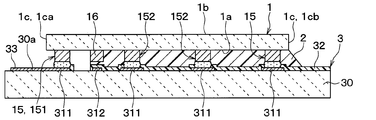
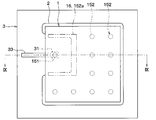
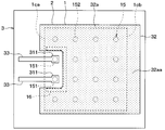
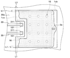
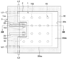
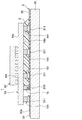
- FIG. 1 is a schematic plan view showing a semiconductor device according to a first embodiment. It is a schematic sectional drawing which shows the cross section between II-II shown with a dashed-dotted line in FIG. It is a schematic sectional drawing which expands and shows the cross-sectional structure of the area
- FIG. 5B is a schematic cross-sectional view illustrating a manufacturing process subsequent to FIG. 5A and a process of forming part of the insulating layer.
- FIG. 5B is a schematic cross-sectional view illustrating a manufacturing process subsequent to FIG. 5B and a process of forming a resist film having a predetermined pattern.
- FIG. 5C is a schematic cross-sectional view illustrating a manufacturing process subsequent to FIG. 5C and a process of forming a rewiring layer and removing a resist film.
- FIG. 5D is a schematic cross-sectional view illustrating a manufacturing process subsequent to FIG. 5D and a process of forming the remaining portion of the insulating layer.
- FIG. 5E is a schematic cross-sectional view showing the manufacturing process subsequent to FIG.
- FIG. 5E is a manufacturing process following Drawing 6A, and is a schematic sectional view showing a process of forming a part of connection part and a wall part.
- FIG. 6B is a schematic cross-sectional view showing a manufacturing step subsequent to FIG. 6B and showing a step of forming the remaining portion of the connecting portion.
- FIG. 6D is a schematic cross-sectional view illustrating a manufacturing process subsequent to FIG. 6C and a resist film removal and reflow process.
- FIG. 6D is a schematic cross-sectional view illustrating a manufacturing process subsequent to FIG. 6D and a process of preparing a substrate and aligning a semiconductor chip.
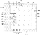
- FIG. 7A It is a manufacturing process following Drawing 7A, and is a schematic sectional view showing a process of junction of a substrate and formation of an underfill. It is a schematic plan view which shows the semiconductor device of 2nd Embodiment. It is a schematic sectional drawing which shows the cross section between IX-IX shown with a dashed-dotted line in FIG. It is a schematic sectional drawing which shows the modification of the semiconductor device of 2nd Embodiment. It is a schematic plan view which shows the semiconductor device of 3rd Embodiment. It is a schematic sectional drawing which shows the cross section between XII-XII shown with a dashed-dotted line in FIG. It is a schematic plan view which shows the semiconductor device of 4th Embodiment.
- the semiconductor device of this embodiment can be applied to a semiconductor device such as a millimeter wave radar mounted on a vehicle such as an automobile.
- FIG. 1 in order to make the configuration easy to understand, constituent elements of a semiconductor chip 1 and a substrate 3 which will be described later and which cannot be seen in a top view are indicated by broken lines or two-dot chain lines.
- FIGS. 1 to 7B in order to make the configuration easy to understand, the dimensions and thicknesses of the constituent elements are deformed and exaggerated.
- FIG. 2 a terminal 12, an insulating layer 13, and a rewiring layer 14 to be described later are omitted from the semiconductor chip 1 for easy understanding.
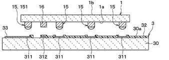
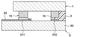
- the semiconductor device of this embodiment includes a semiconductor chip 1, an underfill 2, and a substrate 3, and the semiconductor chip 1 is disposed on the upper surface 30 a of the base material 30 in the substrate 3. While being mounted, the underfill 2 is selectively disposed in these gaps.
- the semiconductor chip 1 is, for example, wafer level chip size package, that is, WLCSP, and is formed by a normal semiconductor process.
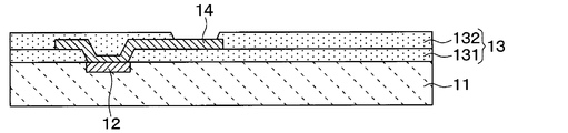
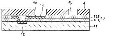
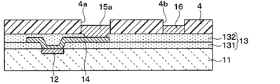
- the semiconductor chip 1 has a substantially plate shape having one surface 1 a and includes a bare chip 11, a terminal 12, an insulating layer 13, a rewiring layer 14, a connection portion 15, and a wall portion 16.
- the terminal 12, the insulating layer 13, the rewiring layer 14, the connection portion 15, and the wall portion 16 are disposed on the one surface 1 a side of the semiconductor chip 1.
- the bare chip 11 is mainly made of a semiconductor material such as silicon, for example, and includes an unillustrated integrated circuit (IC) and has a rectangular plate shape having a surface 11a as shown in FIG. 3, and terminals 12 are provided on the surface 11a side. Is formed.
- IC integrated circuit
- the terminals 12 are made of, for example, a metal material such as Al (aluminum), and a plurality of terminals 12 are arranged in an array as viewed from the normal direction to the surface 11a. As shown in FIG. 3, the terminal 12 is connected to the rewiring layer 14 and covered with an insulating layer 13. The number and arrangement of the plurality of terminals 12 are appropriately changed according to the application.
- the insulating layer 13 is made of, for example, an insulating material used in a normal rewiring process, for example, a resin material such as polyimide.
- the rewiring layer 14 is made of a conductive material used in a normal rewiring process, for example, a metal material such as Cu (copper), Al, Ag (silver), or Au (gold).
- the rewiring layer 14 is formed by, for example, electrolytic plating or electroless plating, and electrically connects the plurality of terminals 12 and the connection portions 15 corresponding to them as shown in FIG.
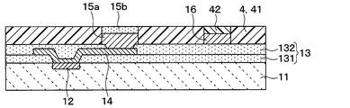
- connection portion 15 is a member that is used when the semiconductor chip 1 is mounted on the substrate 3 and electrically connects the terminal 12 of the semiconductor chip 1 and the wiring formed on the substrate 3. As shown, a plurality are formed and arranged in an array.
- the connecting portion 15 has a structure in which a base layer 15a made of a metal material such as Cu or Ag and a bump 15b made of solder are laminated, and is formed by electrolytic plating or electroless plating. Is done.
- the underlying layer 15a and the bumps 15b are arbitrary in height in the normal direction with respect to the one surface 1a of the semiconductor chip 1.
- the normal direction to the one surface 1a is referred to as “one surface normal direction”
- the height in the one surface normal direction is simply referred to as “height”.
- a part of the plurality of connection parts 15 is a high-frequency connection part 151 used for transmission of a high-frequency signal such as a millimeter wave band with a frequency of 30 GHz to 300 GHz, and the remaining part is used for other purposes.
- the other connection part 152 is used.
- two high-frequency connection portions 151 are disposed at positions adjacent to the outer periphery of the semiconductor chip 1 among the plurality of connection portions 15, that is, at the outermost periphery, as viewed from above. Yes.
- the high-frequency connection portion 151 does not necessarily have to be disposed on the outermost periphery, but is preferably disposed on the outermost periphery from the viewpoint of reducing loss in transmission of a high-frequency signal.
- the high-frequency connection portion 151 is connected to a high-frequency wiring 33 described later, and is partially surrounded by a wall portion 16 described later. Exposed from fill 2.
- one of the two high-frequency connection portions 151 is an output connection portion that transmits a high-frequency signal from the semiconductor chip 1 to the substrate 3, and the other is an input connection that transmits a high-frequency signal from the substrate 3 to the semiconductor chip 1. It is a connection part. Thereby, the loss of the high frequency signal by the underfill 2 comprised with the material from which a dielectric constant differs contacts the high frequency connection part 151 which transmits a high frequency signal is suppressed.
- the wall portion 16 is a member that serves as a wall that prevents the underfill 2 from contacting the high-frequency connection portion 151 in the underfill 2 formation step in the manufacturing process of the semiconductor device of the present embodiment described later. is there.
- the wall portion 16 is made of the same material as that of the base layer 15a in the connection portion 15, and is formed by electrolytic plating, electroless plating, or the like together with the connection portion 15 in the connection portion 15 formation process.
- the wall portion 16 is disposed between the high frequency connection portion 151 and the other connection portion 152 at a position apart from the high frequency connection portion 151 in a top view. These are partitioned. Specifically, for example, as shown in FIG. 1, the wall portion 16 is substantially U-shaped when viewed from above, and the extending direction of the high-frequency wiring 33 to which the high-frequency connection portion 151 is connected. In a different direction, the high-frequency connection portion 151 is partially surrounded.
- the wall portion 16 is arranged with a gap from the substrate 3 as shown in FIG. 2 or FIG. 3, and the height in the normal direction of one surface is smaller than the height of the connection portion 15.
- the wall portion 16 does not come into contact with the substrate 3 when the semiconductor chip 1 is mounted on the substrate 3, and is a material constituting the underfill 2 in the underfill 2 forming step described later. Is high enough to remain in the gap between the wall portion 16 and the substrate 3. Details of the height and shape of the wall 16 will be described later.
- the underfill 2 serves to reinforce the joint portion between the semiconductor chip 1 and the substrate 3, to relieve stress concentration on the joint portion, and to protect by sealing, and is made of a resin material such as an epoxy resin. .
- the underfill 2 is formed by injecting a material made liquid by mixing a resin material with a solvent after the semiconductor chip 1 is mounted on the substrate 3 from the end face side of the semiconductor chip 1 directly under the semiconductor chip 1. Arranged by heat curing.
- the liquid material used for forming the underfill 2 is referred to as an “underfill material”.
- the underfill 2 is selectively filled with a region different from a predetermined region including the high-frequency connection portion 151 in the gap between the semiconductor chip 1 and the substrate 3 as shown in FIG. It is considered as an arrangement. As shown in FIG. 1, the underfill 2 is electrically connected to the high-frequency connection portion 151 in the substrate 3 from the viewpoint of reducing the loss of the high-frequency signal in a region outside the outer periphery of the semiconductor chip 1 in a top view. It is preferable that the arrangement is such that it does not come into contact with the high-frequency wiring 33 connected to.
- the substrate 3 includes a base material 30, a plurality of lands 31, a solder resist layer 32, and a high-frequency wiring 33.
- the substrate 3 may be mounted with other wiring and electronic components (not shown).
- the base material 30 is mainly composed of a synthetic resin such as a polyimide resin, for example, and is formed in a rectangular plate shape having an upper surface 30a as shown in FIG. 1 or 2, and a land 31 and a solder resist layer on the upper surface 30a side. 32 and a high-frequency wiring 33 are arranged.
- a synthetic resin such as a polyimide resin
- the land 31 is made of, for example, a metal material such as Cu, and the connection portion 15 of the semiconductor chip 1 is joined as shown in FIG.
- the land 31 is connected to a high-frequency wiring 33 for transmitting a high-frequency signal, other wiring (not shown), and the like.
- the land 31 is a first land 311 disposed immediately below the connecting portion 15 and a second land disposed directly below the wall portion 16 in a cross-sectional view. And a land 312.
- the second land 312 is used as a dummy for adjusting the dimension in the height direction of a gap between a wall portion 16 and a substrate 3 to be described later, and is connected to the first land 311 and this. Is electrically separated from the wiring.
- the solder resist layer 32 is made of, for example, an insulating material such as polyimide resin, and is formed on the upper surface 30a side as shown in FIG. 2, and a part of the first land 311, the second land 312 and the wiring (not shown). Covers a part of
- the solder resist layer 32 is made of an arbitrary insulating material with good wettability of the liquid underfill material, and this underfill material reaches the high frequency connection portion 151 beyond the wall portion 16. This is a predetermined arrangement for suppressing this. Details of this will be described later.
- the solder resist layer 32 has a thickness in the normal direction with respect to the upper surface 30a of about 50 ⁇ m, for example, but may be adjusted as appropriate.
- the high frequency wiring 33 is made of a metal material such as Cu, and is connected to the first land 311 to which the high frequency connection portion 151 is connected.
- the high-frequency wiring 33 is connected to, for example, an antenna (not shown) and exposed from the underfill 2 as shown in FIG.
- a portion of the substrate 3 that is located immediately below the wall portion 16 in a cross-sectional view is defined as “below the wall” and between the wall portion 16 and the wall directly below. There is a gap.
- gap G 1 is a gap it is preferably less than 10% of G 0.
- the gap G 0 is, for example, 100 ⁇ m to 150 ⁇ m
- the gap G 1 is 15 ⁇ m or less, preferably 5 ⁇ m to 10 ⁇ m.
- the underfill 2 is filled in the gap between the wall portion 16 and the portion immediately below the wall as a result of capillary action in a process of pouring an underfill material in a manufacturing process described later.
- the wall portion 16 is formed at the tip of the wall portion 16 on the substrate 3 side as shown in FIG. 3.
- the cross-sectional shape is a shape having corners, preferably a right-angled shape.
- the portion immediately below the wall of the substrate 3 is composed of the second land 312 and a part of the solder resist layer 32 covering the second land 312 as shown in FIG.
- the portion directly below the wall is formed in a region of the upper surface 30 a of the substrate 3 projected in the normal direction of the surface of the upper surface 30 a of the substrate 3.
- the tip of the wall portion 16 side and the high-frequency connection portion 151 side of the portion directly below the wall has a cross-sectional shape with a corner, preferably a right-angle shape, like the wall portion 16.
- connection part 151 for high frequencies is arrange
- an underfill material is along the high frequency connection part 151 side along these surfaces. It becomes a shape that does not stick out. Therefore, the contact between the underfill 2 and the high frequency connection portion 151 is prevented, and the high frequency connection portion 151 is exposed from the underfill 2.
- the wall 16 in order to easily understand the shape of the wall 16 and the solder resist layer 32, the wall 16, the high frequency connection portion 151, a part of the first land 311, the solder resist layer 32, A part of the high frequency wiring 33 is indicated by a solid line.
- the outline of the semiconductor chip 1 is indicated by a one-dot chain line, and the outline of the first land 311 that is covered with the solder resist layer 32 and is not visible is indicated by a broken line.
- the wall surface on the high frequency connection portion 151 side of the wall portion 16 is referred to as an “inner wall surface 16 a” in the top view, and the wall surface on the opposite side thereof. Is referred to as “outer wall surface 16b".
- the left-right direction in the plane of FIG. 4 is referred to as the “X direction”, and the direction perpendicular to the X direction in the plane of FIG.
- the inner wall surface 16 a of the wall portion 16 is preferably curved at the intersection between the portion along the X direction and the portion along the Y direction when viewed from above. This is because when the underfill material is injected, the underfill material that has reached the gap between the crossing portion and the substrate 3 smoothly flows along the shape of the crossing portion and does not protrude to the high-frequency connection portion 151 side. It is to be done.
- intersection part should just be made into the shape without an angle
- the upper surface 30 a of the base material 30 is connected to the region directly below the semiconductor chip 1 and the region directly below the wall 16 and the high-frequency connection 151 in the top view.
- a part of the area between the first land 311 and the first land 311 is exposed from the solder resist layer 32.
- a region including at least a portion adjacent to a region immediately below the wall portion 16 of the upper surface 30 a of the base material 30 is exposed from the solder resist layer 32.
- a groove penetrating the solder resist layer 32 is formed between the region immediately below the wall portion 16 of the solder resist layer 32 and the first land 311, and the first land 311 is partially formed in the groove. It can be said that it is surrounded.
- an area exposed from the solder resist layer 32 in the upper surface 30 a of the base material 30 is defined as an “exposed area”, and the exposed area is in a state where the wettability of the underfill material is worse than that of the solder resist layer 32.
- the base material 30 is mainly composed of an insulating material whose wettability of the underfill material is worse than that of the solder resist layer 32, or any liquid repellent so that the wettability of the underfill material is deteriorated. Or processing.
- the underfill material becomes the high frequency connection portion 151. Contact is prevented.
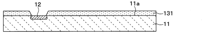
- any semiconductor process can be adopted except that the wall portion 16 is formed in the manufacture of the semiconductor chip 1, and the other steps will be briefly described. 5A to 6D, for easy understanding of the process, a part of the semiconductor chip 1 including the high-frequency connection portion 151 and the wall portion 16 is shown, and the other regions are omitted.
- a bare chip 11 having a plurality of terminals 12 formed on the surface 11a side by a normal semiconductor process is prepared.
- a first insulating film 131 made of a photosensitive insulating material such as polyimide is formed on the surface 11a of the bare chip 11 and is a part of the insulating layer 13, and then photolithography etching is performed. Patterning is performed by the method, and a part of the terminal 12 is exposed.
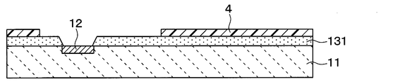
- a seed layer (not shown) covering the first insulating film 131 and a part of the terminal 12 is formed by sputtering or the like.
- This seed layer is formed, for example, by laminating Ti (titanium) and Cu in this order.
- a resist film 4 made of a photosensitive insulating material is formed on the seed layer by a coating method, and is patterned by a photolithography etching method. Expose the surrounding area.
- the resist film 4 is peeled off with a resist stripping solution or the like, and a seed layer (not shown) is removed with an etching solution or the like.
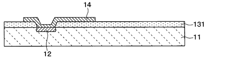
- the second insulating film 132 that covers the rewiring layer 14 and the first insulating film 131 is formed and patterned by the same procedure as described in FIG. 5B, and the surface 11 a of the bare chip 11 and the rewiring layer 14 are then formed.
- An insulating layer 13 is formed to cover a part of the film.
- a portion exposed from the second insulating film 132 in the rewiring layer 14 is defined as an “exposed portion”, and a seed layer (not shown) covering the exposed portion and the second insulating film 132 is formed by sputtering or the like.
- the resist film 4 is formed and patterned on the seed layer by the same procedure as described with reference to FIG. 5C.
- the resist film 4 is provided with an opening 4b that exposes a portion covering the film.
- Ni (not shown) is formed on the base layer 15a and the wall portion 16, as shown in FIG. 6B.
- a (nickel) thin film is formed by electrolytic plating or the like.
- the resist film 4 on the insulating layer 13 is used as the first resist film 41, for example, a second resist film 42 covering the wall portion 16 is formed by dispenser application or the like, and soldering is performed by electrolytic plating or the like.
- Bumps 15b made of are formed on the base layer 15a.
- the bumps 15b made of solder are heated and melted, and then allowed to cool and solidify again.
- the semiconductor chip 1 including the wall portion 16 that partially surrounds the plurality of connection portions 15 and the high-frequency connection portions 151 can be manufactured.
- the first land 311 to which the connecting portion 15 is connected, the second land 312 at a position corresponding to the wall portion 16, the solder resist layer 32 covering these, and the high frequency wiring A substrate 3 including 33 is prepared and aligned with the semiconductor chip 1.
- the bump 15b is heated and melted by a reflow method and then solidified again by being allowed to cool, thereby connecting the semiconductor chip 1 and the substrate 3.
- a liquid underfill material in which an epoxy resin or the like is dissolved with a solvent or the like is poured from the end face of the semiconductor chip 1 directly below the semiconductor chip 1 and is heated and cured to form the underfill 2.
- a surface between one surface 1a and the opposite surface 1b of the semiconductor chip 1 is an end surface 1c, and a portion of the end surface 1c on the high frequency connection portion 151 side in a top view is a first end surface 1ca, and the opposite.
- the underfill material is poured from the second end surface 1cb with the side portion as the second end surface 1cb.
- the wall portion 16 partially surrounds the high frequency connection portion 151, the liquid underfill material is prevented from coming into contact with the high frequency connection portion 151.
- the underfill material is heated and cured to form the underfill 2, whereby the semiconductor device of this embodiment in which the underfill 2 is selectively disposed can be manufactured.
- the semiconductor chip 1 is mounted on the substrate 3, and the high-frequency connection portion 151 that transmits a high-frequency signal is exposed from the underfill 2 in the semiconductor chip 1, and the other connection portions 152 are underfilled.
- a semiconductor device having a structure covered with 2 is obtained. Therefore, the underfill 2 is selectively disposed due to the presence of the wall portion 16, and both relaxation of stress concentration on the other connection portion 152 and reduction in loss in transmission of a high-frequency signal through the high-frequency connection portion 151 are achieved.
- a semiconductor device having the above structure is obtained.
- FIG. 8 as in FIG. 1, the constituent elements of the semiconductor chip 1 and the substrate 3 that are not visible in the top view are shown by broken lines or two-dot chain lines, and the sizes of the constituent elements are deformed and exaggerated. Shows what you did. 8 and 9, as in FIG. 1, the thickness and the like of the components are deformed and exaggerated, and a part of the semiconductor chip 1 is omitted.
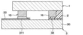
- the wall portion 16 is constituted by the other connection portion 152 adjacent to the high frequency connection portion 151, and is partially exposed from the solder resist layer 32.
- the land 312 is electrically connected.
- the semiconductor device of this embodiment is different from the first embodiment in the above points. In the present embodiment, this difference will be mainly described.
- the wall portion 16 is adjacent to the high-frequency connection portion 151 among the other connection portions 152, and has a wall shape. It is composed of a ground connection portion 152a connected to a portion having a ground potential.
- the wall portion 16 is substantially U-shaped in a top view, and has a high frequency in a direction different from the extending direction of the high frequency wiring 33 to which the high frequency connection portion 151 is connected.
- the connection portion 151 is partially surrounded.
- the wall portion 16 is formed by laminating a base layer 16 c made of a metal material such as Cu or Ag and a bump 16 d made of solder, like the other connection portions 152. It has been configured.
- the wall portion 16 is formed simultaneously with the connection portion 15 by, for example, electrolytic plating or electroless plating.
- the wall portion 16 is connected to the second land 312 that is set to the ground potential in the substrate 3, so that no gap is generated between the wall portion 16 and the substrate 3. It is said that.
- a region between the high-frequency connection portion 151 and the wall portion 16 in the upper surface 30a of the substrate 3 is a solder resist. It may be covered with the layer 32.
- the effects of the first embodiment can be obtained, and a gap is not generated between the wall portion 16 and the substrate 3, so that the underfill 2 is for higher frequencies than the first embodiment.
- a semiconductor device in which contact with the connection portion 151 is suppressed is obtained.
- the wall 16 and the connecting portion 15 have the same configuration and can be formed at the same time, so that an effect of becoming a semiconductor device with reduced manufacturing cost is also expected.
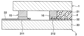
- the semiconductor device of this modification is different from the second embodiment in that the high-frequency connection portion 151, the wall portion 16, and the other connection portion 152 are formed of solder bumps as shown in FIG. To do.
- the semiconductor device of this modification is the same as the semiconductor device of the first embodiment except that the high-frequency connection portion 151, the wall portion 16, and the other connection portion 152 of the semiconductor chip 1 are configured only by bumps made of solder. It can be manufactured by the same manufacturing method. For example, instead of forming the base layer 15a and the wall portion 16 described with reference to FIG. 6B, a bump made of solder is formed by electrolytic plating, and then the resist film 4 and a seed layer (not shown) are removed and reflowed.
- the semiconductor chip 1 used in the example can be prepared.
- the semiconductor device can obtain the same effects as those of the second embodiment.
- FIG. 11 As in FIG. 1, the constituent elements of the semiconductor chip 1 and the substrate 3 that cannot be seen in the top view are indicated by broken lines or two-dot chain lines, and the sizes of the constituent elements are deformed and exaggerated. Shows what you did. 11 and 12, as in FIG. 1, the components are exaggerated by deforming the thickness and the like, and a part of the semiconductor chip 1 is omitted.
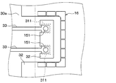
- the semiconductor device according to the present embodiment includes, as a top view, a wall portion 16 that partially surrounds the high-frequency connection portion 151 as a first wall portion 161, and the element portion 17 and the element portion.
- the second embodiment is different from the first embodiment in that it further includes a second wall 162 that surrounds the second wall 162. In the present embodiment, this difference will be mainly described.
- the second wall portion 162 is arranged to surround the element portion 17 in a top view, and has the same configuration as the first wall portion 161 as shown in FIG. Similar to the first wall portion 161, the second wall portion 162 serves as a wall that blocks the underfill material from flowing into a predetermined position. The second wall portion 162 only needs to surround the element portion 17 and prevent the element portion 17 from being covered with the underfill 2, and the position, shape, and the like thereof are changed as appropriate.
- the element unit 17 is formed in the semiconductor chip 1 as shown in FIG. 12, and is configured by, for example, Micro-Electro-Mechanical-Systems, that is, MEMS, and functions as a switch, a sensor, or the like.
- the element unit 17 has, for example, an arbitrary configuration that functions as an actuator, an acceleration sensor, a pressure sensor, and the like, and is formed by an arbitrary semiconductor process.
- the element portion 17 is exposed from the underfill 2 by being surrounded by the second wall portion 162 as shown in FIG. 11 or FIG.
- the substrate 3 projects a predetermined region including the element portion 17 in the semiconductor chip 1, that is, a region projected from the region surrounded by the second wall portion 162 as an “element portion projection region”.
- the through-hole 34 is formed in the element portion projection region.
- the through-hole 34 is a through-hole that connects the upper surface 30a of the base material 30 and the surface on the opposite side, and transmits a signal output from the element unit 17 to an external electronic component (not shown).
- An electrode layer (not shown) is formed on the wall surface as necessary.
- a through hole (not shown) is formed in the element portion projection region of the substrate 3 in addition to the through hole 34.
- the upper surface 30 a has a solder resist as shown in FIG. 12 for the purpose of suppressing the underfill material from flowing into the element portion projection area. Preferably it is exposed from layer 32.
- the wettability of the underfill material deteriorates in the portion where the upper surface 30a of the base material 30 is exposed in the element portion projection region, and the effect of the surface tension in the portion. This suppresses the flow of the underfill material.
- the second wall portion 162 suppresses the contact between the underfill 2 and the element portion 17 and the associated malfunction due to the element portion 17 being provided.
- the resulting semiconductor device is obtained.
- FIGS. 13 and FIG. 14 A fourth embodiment will be described with reference to FIGS.
- the cross section is not shown, but the underfill 2 or the underfill material 2a is hatched.
- the outline and components of the semiconductor chip 1 are indicated by broken lines, the portions hidden by the semiconductor chip 1 in a top view are indicated by solid lines, the sizes of the components, and the like. It shows what was exaggerated by deforming.
- the underfill 2 is generally configured to protrude to the outside of the outline of the semiconductor chip 1 in a top view. At this time, from the viewpoint of reducing the loss of the high frequency signal, the underfill 2 not only does not contact the high frequency connection portion 151 but also does not contact or contact the high frequency wiring 33 in the substrate 3. Is preferably arranged as little as possible.
- the inventors have adjusted the width of the portion of the solder resist layer 32 that protrudes from the semiconductor chip 1 in a top view, and the amount by which the underfill 2 protrudes from the semiconductor chip 1 is controlled. It came to make the semiconductor device of embodiment.
- the amount of the underfill 2 protruding from the semiconductor chip 1 is referred to as “the amount of protrusion”.
- the semiconductor device of the present embodiment is different from the first embodiment in that the amount of protrusion of the underfill 2 is controlled by the solder resist layer 32 in a top view. To do. In the present embodiment, this difference will be mainly described.
- the end face 1 c of the semiconductor chip 1 adjacent to the high frequency connection portion 151 is referred to as a “first end face 1 ca”, and the first end face 1 ca The opposite side is referred to as "second end face 1cb”.
- a region outside the outer periphery of the semiconductor chip 1 in a top view of the solder resist layer 32 is referred to as a “protrusion region 32 a”, and a region where the underfill material is dropped in the protrusion region 32 a. This will be referred to as “dropping region 32aa”.
- the solder resist layer 32 is made of a material with good wettability of the liquid underfill material, that is, a lyophilic material.
- the solder resist layer 32 has an underfill in the region on the opposite side of the semiconductor chip 1 from the straight line formed by the outline of the second end face 1 cb in the top view in the protruding region 32 a. It is set as the dripping area
- the solder resist layer 32 has a constant width L ⁇ b> 1 in a portion different from the dropping region 32 aa in the protruding region 32 a.
- the width L1 is arbitrary, but is, for example, about 0.2 mm to 1 mm.
- the “width of the protruding region 32a” here means a width in a direction perpendicular to the outline of the semiconductor chip 1 with which the protruding region 32a is in contact with the protruding region 32a.
- the width of the protruding region 32a is a width in a region between one side of the outline of the semiconductor chip 1 and a portion outside the one side of the outline of the protruding region 32a.
- the underfill material 2a is dropped and the underfill material 2a is disposed immediately below the semiconductor chip 1 as shown in FIG. Excessive protrusion of 2a can be suppressed.
- the underfill material 2a dropped on the dropping region 32aa is wetted by capillary action in the direction from the second end face 1cb side to the first end face 1ca side as shown by the white arrow in FIG. It spreads.
- the underfill material 2a After the underfill material 2a is first filled in the gap between the semiconductor chip 1 and the substrate 3 except for the portion surrounded by the wall portion 16, the underfill material 2a starts to protrude into the protruding area 32a, and dripping occurs at the start of protruding. Canceled.
- the underfill material 2a is prevented from being uneven in the protruding region. And in the said different area
- the semiconductor device of this embodiment having a configuration in which the amount of the underfill 2 protruding outside the outline of the semiconductor chip 1 is controlled is obtained.
- the amount of protrusion of the underfill 2 from the semiconductor chip 1 is controlled, so that a semiconductor device in which variations in high frequency characteristics are suppressed is obtained.
- the solder resist layer 32 is different from the first embodiment in that blank regions 321 and 322 are formed in portions of the protruding region 32a different from the dropping region 32aa.
- the blank areas 321 and 322 indicate that an unfilled area of the underfill 2 unintentionally, that is, a void is generated in an area immediately below the semiconductor chip 1 when an underfill material is injected directly from the dropping area 32aa to the semiconductor chip 1. Play a role to suppress.
- the underfill material when the underfill material is injected, the underfill material also wraps around the protruding region 32 a, and this wrapping underfill material may spread wet more quickly than the region immediately below the semiconductor chip 1.
- the underfill material wetted and spread in the protruding region 32a surrounds the semiconductor chip 1 in the vicinity of the outer region of the semiconductor chip 1, and air is trapped in the region immediately below the semiconductor chip 1.
- a void occurs.
- the void becomes a starting point for cracking in the underfill 2 or the connection portion 15 due to a temperature change or the like, and may cause a problem.
- the blank area 321 is, for example, one rectangular shape as shown in FIG.
- the blank area 322 has a comb-tooth shape including a plurality of rectangular protrusions.
- the margin areas 321 and 322 need only be able to slow down the wetting and spreading speed of the underfill material when the underfill material wraps around the protruding area 32a, and the number, arrangement, and shape are arbitrary.
- the space between the other semiconductor chip and the substrate on which the semiconductor chip is mounted is filled with an underfill material to suppress voids. It is effective for.
- the semiconductor device of the present embodiment has a configuration in which the amount of protrusion of the underfill 2 is controlled by a region exposed from the solder resist layer 32 in the upper surface 30 a of the substrate 3. This is different from the first embodiment. In the present embodiment, this difference will be mainly described.
- the solder resist layer 32 has a substantially rectangular frame shape surrounding the semiconductor chip 1 in a top view, and is surrounded by the solder resist layer 32 in the base material 30. It is said that the wettability of the underfill material is inferior to that of the part. This is to prevent the underfill material protruding from the outline of the semiconductor chip 1 from getting over the solder resist layer 32 and spreading further outward when the underfill material is injected.
- any part of the upper surface 30a of the base material 30 surrounded by the solder resist layer 32 may be subjected to an arbitrary lyophilic treatment for improving the wettability of the underfill material, or the solder resist layer 32. Any liquid repellent treatment may be applied.
- the relative quality of the underfill material may be adjusted by selecting materials constituting the base material 30 and the solder resist layer 32.
- the underfill 2 is a resist inner region in which a region 30 b surrounded by the inner portion of the solder resist layer 32 in the substrate 3 is defined as a “resist inner region 30 b”. It arrange
- the underfill 2 is disposed in the resist inner region 30 b exposed from the solder resist layer 32, and includes a predetermined high frequency connection portion 151 in the gap between the semiconductor chip 1 and the substrate 3. It covers an area different from the area.
- a region of the resist inner region 30 b that is covered with the underfill 2 and that protrudes from the outer surface of the semiconductor chip 1 is referred to as an “excess region 30 ba”. Further, a region where the underfill material is dropped in the protruding region 30ba is referred to as a “dropping region 30bb”.
- the width in the region different from the dropping region 30bb in the protruding region 30ba is L2, and the width L2 is constant as in the fourth embodiment. This is for controlling the amount of the underfill 2 protruding outside the outer outline of the semiconductor chip 1 as in the fourth embodiment.
- the “width of the protruding region 30ba” here means a width in a direction orthogonal to the outline of the semiconductor chip 1 with which the protruding region 30ba is in contact with the top surface.
- the amount of the underfill 2 protruding from the semiconductor chip 1 is controlled, so that a semiconductor device in which variations in high frequency characteristics are suppressed is obtained.
- FIG. 18 A seventh embodiment will be described with reference to FIG. 18, for the same purpose as in FIG. 17, the semiconductor chip 1 is indicated by a broken line, a portion hidden by the semiconductor chip 1 in a top view is indicated by a solid line, and a region outside the solder resist layer 32 is omitted. Yes.
- the protrusion amount of the underfill 2 is surrounded by the solder resist layer 32 in the upper surface 30 a of the substrate 3 and the resist inner region 30 b exposed from the solder resist layer 32. It is set as the structure controlled by.
- the resist inner region 30b includes blank regions 30bc and 30bd. The semiconductor device of this embodiment is different from the first embodiment in these points. In the present embodiment, this difference will be mainly described.
- the resist inner region 30b is a region where the wettability of the underfill material is better than that of the solder resist layer 32.
- the blank region 30bc , 30bd is shown in FIG. 18, the blank region 30bc , 30bd.
- the blank areas 30bc and 30bd play a role of suppressing the occurrence of unintended voids in the area immediately below the semiconductor chip 1 when the underfill material is injected, like the blank areas 321 and 322 in the fifth embodiment.
- the blank area 30bc is, for example, one rectangular shape as shown in FIG.
- the blank area 30bd has a comb-teeth shape with a plurality of rectangular protrusions.
- the margin areas 30bc and 30bd only have to be able to slow down the wetting and spreading speed of the underfill material when the underfill material wraps around the protruding area 30ba, and the number, arrangement, and shape are arbitrary. .
- the semiconductor device described in each of the above embodiments is an example of the semiconductor device of the present disclosure, and is not limited to each of the above embodiments, and can be appropriately changed.
- the lower portion of the substrate 3 immediately below the wall portion 16 is configured by the second land 312 and part of the solder resist layer 32 has been described.
- the gap G 1 with the wall portion 16 is 10% or less of the gap G 0
- the lower portion of the wall may be composed of only the second land 312 as shown in FIG.
- the second land 312 may be not only a land form but also a wiring form.
- the portion directly below the wall may be configured with only a part of the solder resist layer 32.
- the underfill 2 includes a filler 21 made of an insulating material such as SiO 2 as shown in FIG. It may be configured to include. In this case, as shown in FIG. 21, it is preferable that the filler 21 has a particle size larger than the gap G 1 between the wall portion 16 and the substrate 3.
- the filler 21 is clogged outside the gap between the wall portion 16 and the substrate 3, and the amount of the underfill material entering the gap between the wall portion 16 and the substrate 3 is suppressed. Further, the effect of preventing the underfill 2 from coming into contact with the high-frequency connection 151 is further enhanced. Therefore, the semiconductor device can further reduce the loss of high-frequency signals.
- the particle size of the filler 21 refers to, for example, the arithmetic average diameter in the average particle size distribution.
- the filler 21 may have a particle size larger than the gap between the wall portion 16 and the substrate 3 in a predetermined amount or more, and may have a particle size smaller than the gap between the wall portion 16 and the substrate 3. May be included.
- the wall portion 16 has a shape that partially and continuously surrounds the high-frequency connection portion 151 has been described.
- the shape may be intermittently surrounded.
- the gap between the adjacent wall portions 16 in a top view may be set to such an extent that a capillary phenomenon occurs and the underfill material cannot easily pass therethrough.
- the example in which the high-frequency wiring 33 is exposed from the underfill 2 has been described.
- the structure in which the underfill material is prevented from entering the high-frequency wiring 33 is also possible.
- the semiconductor device may be provided.
- a convex portion or a concave portion that blocks the progress of the liquid underfill material may be formed in a region around the high-frequency wiring 33 in the substrate 3.
- the structure example of the semiconductor device in which the semiconductor chip 1 is WLCSP has been described.
- the semiconductor chip 1 has the interposer substrate 19 and the other surface 19b.
- the wall portion 16 may be formed on the wall.
- the semiconductor chip 1 includes a silicon chip 18 and an interposer substrate 19 having one surface 19a and another surface 19b.
- the silicon chip 18 is a WLCSP, has a configuration including a bare chip, a terminal, an insulating layer, a rewiring layer, and a connection portion 181 (not shown), and is manufactured by a normal semiconductor process.
- the silicon chip 18 is connected to the one surface 19a side of the interposer substrate 19 via a connection portion 181 made of an arbitrary conductive material such as solder or Cu.
- the interposer substrate 19 includes a base material mainly made of an insulating material such as an epoxy resin, for example, and as shown in FIG. 23, a connection portion 191 and a wall portion 16 are formed on the other surface 19b side. Is done.
- the interposer substrate 19 has wirings and through holes (not shown) formed therein, and wirings (not shown) formed on the one surface 19a side are electrically connected to the connection portion 191.
- connection unit 191 corresponds to the connection unit 15 in each of the above embodiments, and a part of the connection unit 191 is used for transmission of a high-frequency signal.
- the arrangement relationship between the connection portion 191 and the wall portion 16 is the same as the arrangement relationship between the connection portion 15 and the wall portion 16 in the above embodiments. That is, the connection portion 191 that is used for transmitting a high-frequency signal is exposed from the underfill 2 by being partially surrounded by the wall portion 16.
- a filler (not shown) that is the same as or different from the underfill 2 may be disposed between the silicon chip 18 and the interposer substrate 19.
- a filler (not shown) that is the same as or different from the underfill 2 may be disposed between the silicon chip 18 and the interposer substrate 19.
Landscapes
- Physics & Mathematics (AREA)
- Condensed Matter Physics & Semiconductors (AREA)
- General Physics & Mathematics (AREA)
- Engineering & Computer Science (AREA)
- Computer Hardware Design (AREA)
- Microelectronics & Electronic Packaging (AREA)
- Power Engineering (AREA)
- Structures Or Materials For Encapsulating Or Coating Semiconductor Devices Or Solid State Devices (AREA)
Applications Claiming Priority (2)
| Application Number | Priority Date | Filing Date | Title |
|---|---|---|---|
| JP2018071779A JP7010116B2 (ja) | 2018-04-03 | 2018-04-03 | 半導体装置 |
| JP2018-071779 | 2018-04-03 |
Publications (1)
| Publication Number | Publication Date |
|---|---|
| WO2019193986A1 true WO2019193986A1 (ja) | 2019-10-10 |
Family
ID=68100712
Family Applications (1)
| Application Number | Title | Priority Date | Filing Date |
|---|---|---|---|
| PCT/JP2019/011947 Ceased WO2019193986A1 (ja) | 2018-04-03 | 2019-03-21 | 半導体装置 |
Country Status (2)
| Country | Link |
|---|---|
| JP (1) | JP7010116B2 (enExample) |
| WO (1) | WO2019193986A1 (enExample) |
Families Citing this family (1)
| Publication number | Priority date | Publication date | Assignee | Title |
|---|---|---|---|---|
| JP7248849B1 (ja) | 2022-08-03 | 2023-03-29 | 株式会社フジクラ | 半導体パッケージおよび高周波モジュール |
Citations (8)
| Publication number | Priority date | Publication date | Assignee | Title |
|---|---|---|---|---|
| JPH0555303A (ja) * | 1991-08-29 | 1993-03-05 | Toshiba Corp | 電子部品装置 |
| JPH06204293A (ja) * | 1992-12-28 | 1994-07-22 | Rohm Co Ltd | 半導体装置 |
| JP2000269384A (ja) * | 1999-03-12 | 2000-09-29 | Nec Corp | マイクロ波・ミリ波回路装置及びその製造方法 |
| JP2006287962A (ja) * | 2006-05-19 | 2006-10-19 | Mitsubishi Electric Corp | 高周波送受信モジュール |
| JP2006344672A (ja) * | 2005-06-07 | 2006-12-21 | Fujitsu Ltd | 半導体チップとそれを用いた半導体装置 |
| JP2007518379A (ja) * | 2004-01-13 | 2007-07-05 | レイセオン・カンパニー | 回路基板組み立て品および回路基板へのチップの取り付け方法 |
| JP2016012704A (ja) * | 2014-06-30 | 2016-01-21 | インターナショナル・ビジネス・マシーンズ・コーポレーションInternational Business Machines Corporation | 接合構造体、接合方法、基板構造体、無線モジュールおよび無線通信装置(伝送経路上を避けて設計された充填材料構造) |
| JP2017098349A (ja) * | 2015-11-20 | 2017-06-01 | 新日本無線株式会社 | 中空パッケージ及びその製造方法 |
-
2018
- 2018-04-03 JP JP2018071779A patent/JP7010116B2/ja active Active
-
2019
- 2019-03-21 WO PCT/JP2019/011947 patent/WO2019193986A1/ja not_active Ceased
Patent Citations (8)
| Publication number | Priority date | Publication date | Assignee | Title |
|---|---|---|---|---|
| JPH0555303A (ja) * | 1991-08-29 | 1993-03-05 | Toshiba Corp | 電子部品装置 |
| JPH06204293A (ja) * | 1992-12-28 | 1994-07-22 | Rohm Co Ltd | 半導体装置 |
| JP2000269384A (ja) * | 1999-03-12 | 2000-09-29 | Nec Corp | マイクロ波・ミリ波回路装置及びその製造方法 |
| JP2007518379A (ja) * | 2004-01-13 | 2007-07-05 | レイセオン・カンパニー | 回路基板組み立て品および回路基板へのチップの取り付け方法 |
| JP2006344672A (ja) * | 2005-06-07 | 2006-12-21 | Fujitsu Ltd | 半導体チップとそれを用いた半導体装置 |
| JP2006287962A (ja) * | 2006-05-19 | 2006-10-19 | Mitsubishi Electric Corp | 高周波送受信モジュール |
| JP2016012704A (ja) * | 2014-06-30 | 2016-01-21 | インターナショナル・ビジネス・マシーンズ・コーポレーションInternational Business Machines Corporation | 接合構造体、接合方法、基板構造体、無線モジュールおよび無線通信装置(伝送経路上を避けて設計された充填材料構造) |
| JP2017098349A (ja) * | 2015-11-20 | 2017-06-01 | 新日本無線株式会社 | 中空パッケージ及びその製造方法 |
Also Published As
| Publication number | Publication date |
|---|---|
| JP2019186281A (ja) | 2019-10-24 |
| JP7010116B2 (ja) | 2022-01-26 |
Similar Documents
| Publication | Publication Date | Title |
|---|---|---|
| US20170250153A1 (en) | Electronic part, electronic device, and electronic apparatus | |
| CN106471612B (zh) | 半导体器件及其制造方法 | |
| US20110283034A1 (en) | Semiconductor chip, and semiconductor package and system each including the semiconductor chip | |
| JP2007287922A (ja) | 積層型半導体装置及びその製造方法 | |
| CN101582395A (zh) | 布线基板 | |
| KR101212661B1 (ko) | 반도체 장치 실장 기판 및 반도체 장치 실장 구조 | |
| KR100250562B1 (ko) | 반도체장치 | |
| JP2006140327A (ja) | 配線基板およびこれを用いた電子部品の実装方法 | |
| EP3971963B1 (en) | Semiconductor package assembly | |
| JP7230462B2 (ja) | 半導体装置およびその製造方法 | |
| CN105374777A (zh) | 倒装芯片封装件及其制造方法 | |
| JP7010116B2 (ja) | 半導体装置 | |
| JP2009135428A (ja) | 実装構造体とその製造方法 | |
| KR20130122218A (ko) | 언더필 플립칩 패키지 제조방법 | |
| JP5229267B2 (ja) | 電子装置 | |
| CA2997607C (en) | Mounting structure and module | |
| JP3850755B2 (ja) | 半導体装置およびその製造方法 | |
| US10573588B2 (en) | Package substrate and semiconductor package including the same | |
| JP2020145318A (ja) | 高周波パッケージ | |
| KR20230001032A (ko) | 반도체 패키지 | |
| KR101869787B1 (ko) | 미세 패턴 및 피치 구현을 위한 배리어층을 갖는 리드 프레임 및 그 제조 방법과, 그 반도체 패키지 | |
| CN223260601U (zh) | 封装结构 | |
| JP4898396B2 (ja) | 弾性波デバイス | |
| JP2007189005A (ja) | 半導体装置の実装構造 | |
| JP4728079B2 (ja) | 半導体装置用基板および半導体装置 |
Legal Events
| Date | Code | Title | Description |
|---|---|---|---|
| 121 | Ep: the epo has been informed by wipo that ep was designated in this application |
Ref document number: 19781723 Country of ref document: EP Kind code of ref document: A1 |
|
| NENP | Non-entry into the national phase |
Ref country code: DE |
|
| 122 | Ep: pct application non-entry in european phase |
Ref document number: 19781723 Country of ref document: EP Kind code of ref document: A1 |