WO2019159342A1 - 電子写真用感光体、その製造方法および電子写真装置 - Google Patents
電子写真用感光体、その製造方法および電子写真装置 Download PDFInfo
- Publication number
- WO2019159342A1 WO2019159342A1 PCT/JP2018/005599 JP2018005599W WO2019159342A1 WO 2019159342 A1 WO2019159342 A1 WO 2019159342A1 JP 2018005599 W JP2018005599 W JP 2018005599W WO 2019159342 A1 WO2019159342 A1 WO 2019159342A1
- Authority
- WO
- WIPO (PCT)
- Prior art keywords
- group
- carbon atoms
- substituent
- layer
- alkyl group
- Prior art date
- Legal status (The legal status is an assumption and is not a legal conclusion. Google has not performed a legal analysis and makes no representation as to the accuracy of the status listed.)
- Ceased
Links
Images


Classifications
-
- G—PHYSICS
- G03—PHOTOGRAPHY; CINEMATOGRAPHY; ANALOGOUS TECHNIQUES USING WAVES OTHER THAN OPTICAL WAVES; ELECTROGRAPHY; HOLOGRAPHY
- G03G—ELECTROGRAPHY; ELECTROPHOTOGRAPHY; MAGNETOGRAPHY
- G03G5/00—Recording-members for original recording by exposure, e.g. to light, to heat or to electrons; Manufacture thereof; Selection of materials therefor
- G03G5/02—Charge-receiving layers
- G03G5/04—Photoconductive layers; Charge-generation layers or charge-transporting layers; Additives therefor; Binders therefor
- G03G5/06—Photoconductive layers; Charge-generation layers or charge-transporting layers; Additives therefor; Binders therefor characterised by the photoconductive material being organic
- G03G5/0601—Acyclic or carbocyclic compounds
- G03G5/0612—Acyclic or carbocyclic compounds containing nitrogen
- G03G5/0614—Amines
- G03G5/06142—Amines arylamine
- G03G5/06147—Amines arylamine alkenylarylamine
- G03G5/061473—Amines arylamine alkenylarylamine plural alkenyl groups linked directly to the same aryl group
-
- G—PHYSICS
- G03—PHOTOGRAPHY; CINEMATOGRAPHY; ANALOGOUS TECHNIQUES USING WAVES OTHER THAN OPTICAL WAVES; ELECTROGRAPHY; HOLOGRAPHY
- G03G—ELECTROGRAPHY; ELECTROPHOTOGRAPHY; MAGNETOGRAPHY
- G03G5/00—Recording-members for original recording by exposure, e.g. to light, to heat or to electrons; Manufacture thereof; Selection of materials therefor
- G03G5/02—Charge-receiving layers
- G03G5/04—Photoconductive layers; Charge-generation layers or charge-transporting layers; Additives therefor; Binders therefor
- G03G5/043—Photoconductive layers characterised by having two or more layers or characterised by their composite structure
- G03G5/047—Photoconductive layers characterised by having two or more layers or characterised by their composite structure characterised by the charge-generation layers or charge transport layers
-
- G—PHYSICS
- G03—PHOTOGRAPHY; CINEMATOGRAPHY; ANALOGOUS TECHNIQUES USING WAVES OTHER THAN OPTICAL WAVES; ELECTROGRAPHY; HOLOGRAPHY
- G03G—ELECTROGRAPHY; ELECTROPHOTOGRAPHY; MAGNETOGRAPHY
- G03G5/00—Recording-members for original recording by exposure, e.g. to light, to heat or to electrons; Manufacture thereof; Selection of materials therefor
- G03G5/02—Charge-receiving layers
- G03G5/04—Photoconductive layers; Charge-generation layers or charge-transporting layers; Additives therefor; Binders therefor
-
- G—PHYSICS
- G03—PHOTOGRAPHY; CINEMATOGRAPHY; ANALOGOUS TECHNIQUES USING WAVES OTHER THAN OPTICAL WAVES; ELECTROGRAPHY; HOLOGRAPHY
- G03G—ELECTROGRAPHY; ELECTROPHOTOGRAPHY; MAGNETOGRAPHY
- G03G5/00—Recording-members for original recording by exposure, e.g. to light, to heat or to electrons; Manufacture thereof; Selection of materials therefor
- G03G5/02—Charge-receiving layers
- G03G5/04—Photoconductive layers; Charge-generation layers or charge-transporting layers; Additives therefor; Binders therefor
- G03G5/05—Organic bonding materials; Methods for coating a substrate with a photoconductive layer; Inert supplements for use in photoconductive layers
- G03G5/0525—Coating methods
-
- G—PHYSICS
- G03—PHOTOGRAPHY; CINEMATOGRAPHY; ANALOGOUS TECHNIQUES USING WAVES OTHER THAN OPTICAL WAVES; ELECTROGRAPHY; HOLOGRAPHY
- G03G—ELECTROGRAPHY; ELECTROPHOTOGRAPHY; MAGNETOGRAPHY
- G03G5/00—Recording-members for original recording by exposure, e.g. to light, to heat or to electrons; Manufacture thereof; Selection of materials therefor
- G03G5/02—Charge-receiving layers
- G03G5/04—Photoconductive layers; Charge-generation layers or charge-transporting layers; Additives therefor; Binders therefor
- G03G5/05—Organic bonding materials; Methods for coating a substrate with a photoconductive layer; Inert supplements for use in photoconductive layers
- G03G5/0528—Macromolecular bonding materials
- G03G5/0557—Macromolecular bonding materials obtained otherwise than by reactions only involving carbon-to-carbon unsatured bonds
- G03G5/0564—Polycarbonates
-
- G—PHYSICS
- G03—PHOTOGRAPHY; CINEMATOGRAPHY; ANALOGOUS TECHNIQUES USING WAVES OTHER THAN OPTICAL WAVES; ELECTROGRAPHY; HOLOGRAPHY
- G03G—ELECTROGRAPHY; ELECTROPHOTOGRAPHY; MAGNETOGRAPHY
- G03G5/00—Recording-members for original recording by exposure, e.g. to light, to heat or to electrons; Manufacture thereof; Selection of materials therefor
- G03G5/02—Charge-receiving layers
- G03G5/04—Photoconductive layers; Charge-generation layers or charge-transporting layers; Additives therefor; Binders therefor
- G03G5/06—Photoconductive layers; Charge-generation layers or charge-transporting layers; Additives therefor; Binders therefor characterised by the photoconductive material being organic
- G03G5/0601—Acyclic or carbocyclic compounds
- G03G5/0605—Carbocyclic compounds
- G03G5/0607—Carbocyclic compounds containing at least one non-six-membered ring
-
- G—PHYSICS
- G03—PHOTOGRAPHY; CINEMATOGRAPHY; ANALOGOUS TECHNIQUES USING WAVES OTHER THAN OPTICAL WAVES; ELECTROGRAPHY; HOLOGRAPHY
- G03G—ELECTROGRAPHY; ELECTROPHOTOGRAPHY; MAGNETOGRAPHY
- G03G5/00—Recording-members for original recording by exposure, e.g. to light, to heat or to electrons; Manufacture thereof; Selection of materials therefor
- G03G5/02—Charge-receiving layers
- G03G5/04—Photoconductive layers; Charge-generation layers or charge-transporting layers; Additives therefor; Binders therefor
- G03G5/06—Photoconductive layers; Charge-generation layers or charge-transporting layers; Additives therefor; Binders therefor characterised by the photoconductive material being organic
- G03G5/0601—Acyclic or carbocyclic compounds
- G03G5/0609—Acyclic or carbocyclic compounds containing oxygen
-
- G—PHYSICS
- G03—PHOTOGRAPHY; CINEMATOGRAPHY; ANALOGOUS TECHNIQUES USING WAVES OTHER THAN OPTICAL WAVES; ELECTROGRAPHY; HOLOGRAPHY
- G03G—ELECTROGRAPHY; ELECTROPHOTOGRAPHY; MAGNETOGRAPHY
- G03G5/00—Recording-members for original recording by exposure, e.g. to light, to heat or to electrons; Manufacture thereof; Selection of materials therefor
- G03G5/02—Charge-receiving layers
- G03G5/04—Photoconductive layers; Charge-generation layers or charge-transporting layers; Additives therefor; Binders therefor
- G03G5/06—Photoconductive layers; Charge-generation layers or charge-transporting layers; Additives therefor; Binders therefor characterised by the photoconductive material being organic
- G03G5/0601—Acyclic or carbocyclic compounds
- G03G5/0612—Acyclic or carbocyclic compounds containing nitrogen
- G03G5/0616—Hydrazines; Hydrazones
-
- G—PHYSICS
- G03—PHOTOGRAPHY; CINEMATOGRAPHY; ANALOGOUS TECHNIQUES USING WAVES OTHER THAN OPTICAL WAVES; ELECTROGRAPHY; HOLOGRAPHY
- G03G—ELECTROGRAPHY; ELECTROPHOTOGRAPHY; MAGNETOGRAPHY
- G03G5/00—Recording-members for original recording by exposure, e.g. to light, to heat or to electrons; Manufacture thereof; Selection of materials therefor
- G03G5/02—Charge-receiving layers
- G03G5/04—Photoconductive layers; Charge-generation layers or charge-transporting layers; Additives therefor; Binders therefor
- G03G5/06—Photoconductive layers; Charge-generation layers or charge-transporting layers; Additives therefor; Binders therefor characterised by the photoconductive material being organic
- G03G5/0601—Acyclic or carbocyclic compounds
- G03G5/0618—Acyclic or carbocyclic compounds containing oxygen and nitrogen
-
- G—PHYSICS
- G03—PHOTOGRAPHY; CINEMATOGRAPHY; ANALOGOUS TECHNIQUES USING WAVES OTHER THAN OPTICAL WAVES; ELECTROGRAPHY; HOLOGRAPHY
- G03G—ELECTROGRAPHY; ELECTROPHOTOGRAPHY; MAGNETOGRAPHY
- G03G5/00—Recording-members for original recording by exposure, e.g. to light, to heat or to electrons; Manufacture thereof; Selection of materials therefor
- G03G5/02—Charge-receiving layers
- G03G5/04—Photoconductive layers; Charge-generation layers or charge-transporting layers; Additives therefor; Binders therefor
- G03G5/06—Photoconductive layers; Charge-generation layers or charge-transporting layers; Additives therefor; Binders therefor characterised by the photoconductive material being organic
- G03G5/0622—Heterocyclic compounds
- G03G5/0624—Heterocyclic compounds containing one hetero ring
- G03G5/0627—Heterocyclic compounds containing one hetero ring being five-membered
- G03G5/0631—Heterocyclic compounds containing one hetero ring being five-membered containing two hetero atoms
-
- G—PHYSICS
- G03—PHOTOGRAPHY; CINEMATOGRAPHY; ANALOGOUS TECHNIQUES USING WAVES OTHER THAN OPTICAL WAVES; ELECTROGRAPHY; HOLOGRAPHY
- G03G—ELECTROGRAPHY; ELECTROPHOTOGRAPHY; MAGNETOGRAPHY
- G03G5/00—Recording-members for original recording by exposure, e.g. to light, to heat or to electrons; Manufacture thereof; Selection of materials therefor
- G03G5/02—Charge-receiving layers
- G03G5/04—Photoconductive layers; Charge-generation layers or charge-transporting layers; Additives therefor; Binders therefor
- G03G5/06—Photoconductive layers; Charge-generation layers or charge-transporting layers; Additives therefor; Binders therefor characterised by the photoconductive material being organic
- G03G5/0664—Dyes
- G03G5/0666—Dyes containing a methine or polymethine group
- G03G5/0672—Dyes containing a methine or polymethine group containing two or more methine or polymethine groups
Definitions
- the present invention relates to an electrophotographic photoreceptor (hereinafter also referred to as “photoreceptor”), a manufacturing method thereof, and an electrophotographic apparatus. More particularly, the present invention relates to an electrophotographic photoreceptor, which is mainly composed of a conductive substrate and a photosensitive layer containing an organic material, and is used in an electrophotographic printer, a copying machine, a fax machine, etc., a manufacturing method thereof, and an electrophotographic apparatus. .
- the electrophotographic photoreceptor has a basic structure in which a photosensitive layer having a photoconductive function is provided on a conductive substrate.
- organic electrophotographic photoreceptors that use organic compounds as functional components responsible for charge generation and transport have been actively researched and developed due to advantages such as material diversity, high productivity, and safety. Application to printers and printers is ongoing.
- organic photoreceptors are required to have a long service life from the viewpoint of increasing the number of printed sheets per electrophotographic apparatus by centralized printing accompanying networking in an office and reducing running costs.
- the organic photoreceptor in order to reduce the cost, is required to have a smaller diameter along with the downsizing of the machine.
- the surface layer of the photoreceptor is generally formed mainly from a charge transport material and a binder resin. In order to ensure the printing durability of the photoreceptor surface, the molecular structure of the binder resin and its content are important.
- a photoreceptor needs to have a function of holding a surface charge in a dark place, a function of generating a charge by receiving light, and a function of transporting the generated charge.
- a so-called single-layer type photoreceptor having a photosensitive layer, a charge generation layer mainly responsible for charge generation during photoreception, a function for retaining surface charges in the dark, and a charge generation layer during photoreception There is a so-called laminated type (functional separation type) photoconductor including a photosensitive layer in which a functionally separated layer is laminated on a charge transporting layer having a function of transporting generated charges.
- the photosensitive layer is generally formed by applying a coating solution in which a charge generating substance, a charge transporting substance and a binder resin are dissolved or dispersed in an organic solvent on a conductive substrate.
- organic electrophotographic photoreceptors particularly the outermost layer, are resistant to friction generated between paper and a blade for removing toner, have excellent flexibility, and have good exposure transparency.
- polycarbonate is used as a binder resin.
- bisphenol Z-type polycarbonate is widely used as the binder resin. A technique using such a polycarbonate as a binder resin is described in Patent Document 1 and the like.
- a charging member such as scorotron
- a charging member such as a non-contact charging method in which the charging member and the photosensitive member are not in contact
- a charging member such as a semiconductive rubber roller or brush
- the contact charging method has the advantage that less ozone is generated and the applied voltage may be lower because corona discharge occurs in the very vicinity of the photoreceptor compared to the non-contact charging method. Therefore, since a more compact, low-cost, and low environmental pollution electrophotographic apparatus can be realized, it is mainly used for medium-sized to small-sized apparatuses.
- a means for cleaning the surface of the photoreceptor scraping with a blade, a simultaneous development cleaning process, and the like are mainly used.
- the untransferred residual toner on the surface of the organic photoreceptor is scraped off by the blade, and the toner is collected in a waste toner box or returned to the developing device again.
- the apparatus requires a toner collection box for collecting the scraped toner and a space for recycling the scraped toner. It is also necessary to monitor fullness.
- paper dust or external additives stay on the blade, the surface of the organic photoreceptor may be damaged to shorten the life of the photoreceptor.
- toner with varying charge amount is generated in the contact charging mechanism.
- a contactless mechanism when used and a cleaningless mechanism that performs development and cleaning with a developing device is used, toner with varying charge amount is generated in the contact charging mechanism.
- toner when there is a reverse polarity toner mixed in a very small amount, there is a problem that these toners cannot be sufficiently removed from the surface of the photoreceptor and the charging device is contaminated.
- the surface of the photoconductor may be contaminated by ozone, nitrogen oxide, or the like generated when the photoconductor is charged.
- the adhered substances reduce the lubricity of the surface of the photoreceptor, making it easier for paper dust and toner to adhere, causing blade noise, turning over, and scratches on the surface. There is also.
- Patent Documents 2 and 3 propose a method of adding a filler to the surface layer of the photosensitive layer in order to improve the durability of the surface of the photoreceptor.
- the method of dispersing the filler in such a film has a problem that it is difficult to uniformly disperse the filler.
- filler aggregates are present, film permeability is reduced, and exposure light is scattered by the filler, resulting in non-uniform charge transport and charge generation, resulting in poor image characteristics.
- there is a method of adding a dispersant to improve the filler dispersibility since the dispersant itself affects the photoreceptor characteristics, it is difficult to achieve compatibility with the filler dispersibility.
- Patent Document 4 proposes a method of incorporating a fluororesin such as polytetrafluoroethylene (PTFE) into the photosensitive layer
- Patent Document 5 proposes a method of adding a silicone resin such as alkyl-modified polysiloxane.
- PTFE polytetrafluoroethylene
- Patent Document 5 proposes a method of adding a silicone resin such as alkyl-modified polysiloxane.
- a fluororesin such as PTFE has low solubility in a solvent or poor compatibility with other resins, so that phase separation causes light scattering at the resin interface. There is. Therefore, the sensitivity characteristic as a photoconductor cannot be satisfied.
- the method described in Patent Document 5 has a problem that the effect cannot be obtained continuously because the silicone resin bleeds to the surface of the coating film.
- Patent Documents 6, 7 and 8 disclose a photoconductor having improved durability by incorporating a high mobility hole transport agent as a charge transport agent in the charge transport layer. Proposed.
- a photoreceptor also has a problem that the wear resistance is still insufficient due to the combination of resins.
- a method for forming a surface protective layer on the photosensitive layer has been proposed for the purpose of protecting the photosensitive layer, improving mechanical strength, and improving surface lubricity.
- these methods for forming the surface protective layer have problems that it is difficult to form a film on the charge transport layer and that it is difficult to achieve both the charge transport performance and the charge retention function.
- the organic material as the photosensitive material has many advantages not found in the inorganic material, but a material that sufficiently satisfies all the characteristics required for the electrophotographic photosensitive member has not been obtained. Is the current situation. That is, the image quality is deteriorated due to a decrease in charging potential, an increase in residual potential, a change in sensitivity, and the like due to repeated use. The cause of this deterioration has not been fully clarified, but as one of the factors, the resin is exposed to repeated exposure to light from image exposure and static elimination lamps, and from external light during maintenance. Photodegradation or charge transport material may be decomposed.
- JP-A-61-62040 JP-A-1-205171 Japanese Patent Laid-Open No. 7-333881 JP-A-4-368953 JP 2002-162759 A JP 2000-66419 A JP 2000-47405 A JP 2013-25189 A JP-A-11-160958 JP 2008-164757 A
- the object of the present invention is to eliminate the above-mentioned problems, and to provide high sensitivity, low residual potential, excellent wear resistance and stain resistance without providing a surface protective layer on the photosensitive layer.
- An object of the present invention is to provide an electrophotographic photoreceptor, a method for producing the same, and an electrophotographic apparatus that are less prone to light fatigue and filming and that have excellent potential stability before and after repeated printing.
- the present inventors have found that a specific high mobility hole transport material, polycarbonate resin, and electron transport material are contained in the photosensitive layer located on the outermost surface of the photoreceptor. By containing it, the components that exude from the components in the device such as the charging roller are prevented from entering the photoconductor, thereby improving the anti-contamination property and improving the wear resistance, and further, light fatigue and filming. It has been found that the potential stability before and after repeated printing can be ensured, and the present invention has been completed.
- the first aspect of the present invention is an electrophotographic photoreceptor including a conductive substrate and a photosensitive layer provided on the conductive substrate.
- the photosensitive layer comprises a hole transport material having a structure represented by the following general formula (1), a binder resin having a repeating structure represented by the following general formula (2), and the following general formulas (ET1) to (ET3) And at least one of electron transport materials having a structure represented by the formula:
- R 1 represents a hydrogen atom or an alkyl group having 1 to 3 carbon atoms which may have a substituent
- R 2 to R 11 each independently represents a hydrogen atom, a halogen atom, or a substituent.
- R 12 to R 15 are the same or different and each represents a hydrogen atom, an alkyl group having 1 to 10 carbon atoms or a fluoroalkyl group having 1 to 10 carbon atoms, and g, h, k, p Is an integer of 0 to 4, s and t satisfy 0.3 ⁇ t / (s + t) ⁇ 0.7, and the chain end group is a monovalent aromatic group or a monovalent fluorine-containing aliphatic group.
- R 16 and R 17 are the same or different and are a hydrogen atom, an alkyl group having 1 to 12 carbon atoms, an alkoxy group having 1 to 12 carbon atoms, or an aryl group which may have a substituent.
- R 18 represents a hydrogen atom, an alkyl group having 1 to 6 carbon atoms, an alkoxy group having 1 to 6 carbon atoms, or a substituent.
- R 19 to R 23 may be the same or different and represent a hydrogen atom, a halogen atom, a carbon
- the substituent is a halogen atom, an alkyl group having 1 to 6 carbon atoms, 6 represents an alkoxy group, a hydroxyl group, a cyano group, an amino group, a nitro group or a halogenated alkyl group)
- R 24 to R 29 are the same or different and are a hydrogen atom, a halogen atom, a cyano group, a nitro group, a hydroxyl group, an alkyl group having 1 to 12 carbon atoms, or an alkoxy group having 1 to 12 carbon atoms.
- R 30 and R 31 are the same or different and each represents a hydrogen atom, an alkyl group having 1 to 12 carbon atoms, an alkoxy group having 1 to 12 carbon atoms, or an ary
- the above general formula (1) having high mobility as a hole transport material. High sensitivity can be maintained even if the mass ratio of the binder resin that contributes to wear resistance is increased by using a compound having a structure represented by the formula, realizing both high wear resistance and high sensitivity. can do.
- the polycarbonate resin represented by the general formula (2) is inferior in light resistance to ultraviolet light and gas resistance to active gases such as ozone. Therefore, by using an electron transport material having a structure represented by the above general formulas (ET1) to (ET3) that absorbs in the ultraviolet region in the role of an ultraviolet light absorber, high light resistance and repeated potential stability can be obtained. Can be realized.
- the photosensitive layer includes a charge generation layer and a charge transport layer sequentially stacked on the conductive substrate, and the charge transport layer includes the hole transport material, the binder resin, and the electron transport. It can contain substances.
- the hole mobility of the hole transport material is 60 ⁇ 10 ⁇ 6 [cm 2 / V ⁇ s] or more
- the content of the binder resin in the charge transport layer is the solid content of the charge transport layer. It is preferable that it is 55 mass% or more and 85 mass% or less with respect to a minute.
- the photosensitive layer may include the hole transport material, the binder resin, and the electron transport material in a single layer.
- the hole mobility of the hole transport material is 60 ⁇ 10 ⁇ 6 [cm 2 / V ⁇ s] or more
- the content of the binder resin in the photosensitive layer is equal to the solid content of the photosensitive layer. It is preferable that it is 55 mass% or more and 85 mass% or less.
- the photosensitive layer includes a charge transport layer and a charge generation layer sequentially stacked on the conductive substrate, and the charge generation layer includes the hole transport material, the binder resin, and the electron transport material. Can be included.
- the hole transport material has a hole mobility of 60 ⁇ 10 ⁇ 6 [cm 2 / V ⁇ s] or more, and the content of the binder resin in the charge generation layer is a solid content of the charge generation layer. It is preferable that it is 55 mass% or more and 85 mass% or less with respect to a minute.
- the second aspect of the present invention is an electrophotographic photoreceptor comprising a step of forming a photosensitive layer by applying a coating solution on the conductive substrate in producing the electrophotographic photoreceptor.
- a manufacturing method comprising: A hole transport material having a structure represented by the general formula (1), a binder resin having a repeating structure represented by the general formula (2), and a structure represented by the general formulas (ET1) to (ET3). And a step of preparing the coating liquid containing at least one kind of electron transport materials.
- a third aspect of the present invention is an electrophotographic apparatus equipped with the electrophotographic photosensitive member.
- the present invention even if a surface protective layer is not provided on the photosensitive layer, it has high sensitivity, low residual potential, excellent wear resistance and stain resistance, photo fatigue and filming. It is possible to realize an electrophotographic photosensitive member, a method for producing the same, and an electrophotographic apparatus that are less likely to cause oxidization and have excellent potential stability before and after repeated printing.
- FIG. 1 is a schematic cross-sectional view showing an example of an electrophotographic photoreceptor of the present invention.
- FIG. 6 is a schematic cross-sectional view showing another example of the electrophotographic photoreceptor of the present invention.
- FIG. 6 is a schematic cross-sectional view showing still another example of the electrophotographic photoreceptor of the present invention. It is a schematic block diagram which shows an example of the electrophotographic apparatus of this invention.
- FIG. 1 is a schematic cross-sectional view showing an example of the electrophotographic photoreceptor of the present invention, and shows a negatively charged laminated electrophotographic photoreceptor.
- a charge generation layer 4 having a charge generation function and a charge transport layer 5 having a charge transport function are provided on a conductive substrate 1 via an undercoat layer 2.
- a negatively charged laminated type photosensitive layer 6 is provided in which are sequentially laminated.
- FIG. 2 is a schematic cross-sectional view showing another example of the electrophotographic photoreceptor of the present invention, and shows a positively charged single-layer electrophotographic photoreceptor.
- a positively charged single layer type photosensitive layer 3 having both a charge generation function and a charge transport function via an undercoat layer 2 on a conductive substrate 1.
- a positively charged single layer type photosensitive layer 3 having both a charge generation function and a charge transport function via an undercoat layer 2 on a conductive substrate 1.
- a positively charged single layer type photosensitive layer 3 having both a charge generation function and a charge transport function via an undercoat layer 2 on a conductive substrate 1.
- FIG. 3 is a schematic sectional view showing still another example of the electrophotographic photoreceptor of the present invention, and shows a positively charged laminated electrophotographic photoreceptor.
- the charge transport layer 5 having a charge transport function and the charge generating function and the charge transport function are provided on the conductive substrate 1 via the undercoat layer 2.
- a positively charged laminated type photosensitive layer 7 is provided in which the generation layer 4 is sequentially laminated.
- the undercoat layer 2 may be provided as necessary.
- the “photosensitive layer” of the present invention includes both a laminated photosensitive layer in which a charge generation layer and a charge transport layer are laminated, and a single-layer type photosensitive layer.
- a photoreceptor includes a conductive substrate and a photosensitive layer provided on the conductive substrate, and the photosensitive layer has a structure represented by the general formula (1). And a binder resin having a repeating structure represented by the general formula (2) and at least one of electron transport materials having the structures represented by the general formulas (ET1) to (ET3) It is. This eliminates the need to provide a surface protective layer on the photosensitive layer. It has high sensitivity, low residual potential, excellent wear resistance and stain resistance, is resistant to light fatigue and filming, and is repeatedly printed. A photoconductor excellent in potential stability before and after can be obtained.
- the hole transport material a material having a high mobility is preferably used.
- the hole mobility is 40 ⁇ 10 ⁇ 6 to 120 ⁇ 10 ⁇ 6 when the electric field strength is 20 V / ⁇ m. cm 2 / V ⁇ s], particularly 60 ⁇ 10 ⁇ 6 to 120 ⁇ 10 ⁇ 6 [cm 2 / V ⁇ s], and further 70 ⁇ 10 ⁇ 6 to 120 ⁇ 10 ⁇ 6 [cm 2 / V ⁇ s] ] Is preferable.
- a hole transport material in which a substituent is bonded to a meta position or a para position with respect to the benzene ring having R 1 is preferable.
- the said hole mobility can be measured using the coating liquid obtained by adding a hole transport material so that it may become 50 mass% in binder resin.
- the ratio of hole transport material to resin binder is 50:50.
- the binder resin may be a bisphenol Z type polycarbonate resin.
- Iupizeta PCZ-500 (trade name, manufactured by Mitsubishi Gas Chemical Co., Ltd.) may be used.
- this coating solution is applied onto a substrate, dried at 120 ° C. for 30 minutes to prepare a coating film having a film thickness of 7 ⁇ m, and a constant electric field strength of 20 V using a TOF (Time of Flight) method.
- the hole mobility at / ⁇ m can be measured.
- the measurement temperature is 300K.
- the ratio of s and t preferably satisfies 0.3 ⁇ t / (s + t) ⁇ 0.7, and the chain end group is a monovalent aromatic group or a monovalent fluorine-containing aliphatic group. It is preferable.
- t / (s + t) By setting t / (s + t) to 0.3 or more, both wear resistance and contamination resistance can be secured satisfactorily, and by setting t / (s + t) to 0.7 or less, synthesis of the resin is easy. Become.
- the conductive substrate 1 serves as a support for each layer constituting the photoconductor as well as serving as an electrode of the photoconductor, and may have any shape such as a cylindrical shape, a plate shape, or a film shape.
- a metal such as aluminum, stainless steel, nickel, or the like such as a glass, resin, or the like subjected to a conductive treatment can be used.
- the undercoat layer 2 is composed of a resin-based layer or a metal oxide film such as alumite.
- the undercoat layer 2 is used to control the charge injection property from the conductive substrate 1 to the photosensitive layer, or to cover defects on the surface of the conductive substrate 1 and to improve the adhesion between the photosensitive layer and the conductive substrate 1. It is provided as necessary for the purpose.
- the resin material used for the undercoat layer 2 include insulating polymers such as casein, polyvinyl alcohol, polyamide, melamine, and cellulose, and conductive polymers such as polythiophene, polypyrrole, and polyaniline. These resins are used alone, Alternatively, they can be used in combination as appropriate. These resins may be used by containing a metal oxide such as titanium dioxide or zinc oxide.
- the photosensitive layer may be any one of the negatively charged laminated type photosensitive layer 6, the positively charged single layer type photosensitive layer 3, and the positively charged laminated type photosensitive layer 7.
- the charge transport layer 5 contains the specific hole transporting material, the binder resin and the electron transporting material.
- the positively charged laminated type photosensitive layer 7 charge generation occurs.
- the layer 4 contains the specific hole transport material, binder resin, and electron transport material.
- the charge generation layer 4 is formed by a method such as applying a coating solution in which particles of a charge generation material are dispersed in a binder resin, and receives light to generate charges.
- the charge generation layer 4 has a high charge generation efficiency, and at the same time, it is important to inject the generated charges into the charge transport layer 5.
- the charge generation layer 4 has a low electric field dependency and is preferably injected even in a low electric field.
- charge generation materials include phthalocyanines such as X-type metal-free phthalocyanine, ⁇ -type metal-free phthalocyanine, ⁇ -type titanyl phthalocyanine, ⁇ -type titanyl phthalocyanine, Y-type titanyl phthalocyanine, ⁇ -type titanyl phthalocyanine, amorphous-type titanyl phthalocyanine, and ⁇ -type copper phthalocyanine.
- phthalocyanines such as X-type metal-free phthalocyanine, ⁇ -type metal-free phthalocyanine, ⁇ -type titanyl phthalocyanine, ⁇ -type titanyl phthalocyanine, Y-type titanyl phthalocyanine, ⁇ -type titanyl phthalocyanine, amorphous-type titanyl phthalocyanine, and ⁇ -type copper phthalocyanine.
- binder resin used for the charge generation layer 4 polycarbonate resin, polyester resin, polyamide resin, polyurethane resin, vinyl chloride resin, vinyl acetate resin, phenoxy resin, polyvinyl acetal resin, polyvinyl butyral resin, polystyrene resin, polysulfone resin, diallyl phthalate Resins, polymers and copolymers of methacrylic ester resins, and the like can be used in appropriate combination.
- the charge generation layer 4 since the charge generation layer 4 only needs to have a charge generation function, its film thickness is determined by the light absorption coefficient of the charge generation material, and is generally 1 ⁇ m or less, preferably 0.5 ⁇ m or less.
- the charge generation layer 4 can also be used with a charge generation material as a main component and a charge transport material added thereto.
- the content of the binder resin in the charge generation layer 4 is preferably 20 to 80% by mass, more preferably 30 to 70% by mass with respect to the solid content of the charge generation layer 4.
- the content of the charge generation material in the charge generation layer 4 is preferably 20 to 80% by mass, more preferably 30 to 70% by mass with respect to the solid content of the charge generation layer 4.
- the charge transport layer 5 is a hole transport material having a structure represented by the general formula (1), a binder resin having a repeating unit represented by the general formula (2), And at least one of electron transport materials having a structure represented by the general formulas (ET1) to (ET3).
- hole transport materials can be used in combination as required, as long as the effects of the present invention are not significantly impaired.
- Other known hole transport materials include, for example, hydrazone compounds, pyrazoline compounds, pyrazolone compounds, oxadiazole compounds, oxazole compounds, arylamine compounds, benzidine compounds, stilbene compounds, styryl compounds, enamine compounds, butadiene compounds, polyvinyl carbazoles Polysilane or the like can be used singly or in combination of two or more.
- binder resins can be used in combination with the charge transport layer 5 as necessary, as long as the effects of the present invention are not significantly impaired.
- Other known binder resins include, for example, polycarbonate resins other than the copolymer polycarbonate resin represented by the general formula (1), polyarylate resins, polyester resins, polyvinyl acetal resins, polyvinyl butyral resins, polyvinyl alcohol resins, and vinyl chloride.
- Thermoplastic resins such as resins, vinyl acetate resins, polyethylene resins, polypropylene resins, polystyrene resins, acrylic resins, polyamide resins, ketone resins, polyacetal resins, polysulfone resins, methacrylate esters, alkyd resins, epoxy resins, silicon Resin, urea resin, phenolic resin, unsaturated polyester resin, polyurethane resin, melamine resin and other thermosetting resins, and copolymers thereof are used in appropriate combination of one or more. It is possible to.
- the charge transport layer 5 can be used in combination with other known electron transport materials as needed, as long as the effects of the present invention are not significantly impaired.
- Other known electron transport materials include succinic anhydride, maleic anhydride, dibromosuccinic anhydride, phthalic anhydride, 3-nitrophthalic anhydride, 4-nitrophthalic anhydride, pyromellitic anhydride, pyromellitic acid, trimethyl Mellitic acid, trimellitic anhydride, phthalimide, 4-nitrophthalimide, tetracyanoethylene, tetracyanoquinodimethane, chloranil, bromanyl, o-nitrobenzoic acid, malononitrile, trinitrofluorenone, trinitrothioxanthone, dinitrobenzene, dinitroanthracene , Dinitroacridine, nitroanthraquinone, dinitroanthraquinone, thiopyran compounds, quinone compounds, benzoquinone compounds, dipheno
- the content of the binder resin in the charge transport layer 5 is preferably 55 to 85% by mass, more preferably 60 to 75% by mass, based on the solid content of the charge transport layer 5.
- the content of the hole transport material in the charge transport layer 5 is preferably 20 to 80 parts by mass, more preferably 30 to 70 parts by mass with respect to 100 parts by mass of the binder resin.
- the content of the electron transport material in the charge transport layer 5 is preferably 1 to 10 parts by mass, more preferably 3 to 5 parts by mass with respect to 100 parts by mass of the binder resin.
- the film thickness of the charge transport layer 5 is preferably 5 to 60 ⁇ m, more preferably 10 to 40 ⁇ m in order to maintain a practically effective surface potential.
- the positively charged single layer type photosensitive layer 3 includes a compound having a structure represented by the above general formula (1) as a hole transport material and the above general formula (2) as a binder resin. ) And a resin having a repeating unit, and at least one compound having a structure represented by the general formulas (ET1) to (ET3) as an electron transporting material, and a charge generating material. Can be configured. Thereby, the desired effect of the present invention can be obtained.
- Examples of the charge generation material used for the photosensitive layer 3 include phthalocyanine pigments, azo pigments, anthanthrone pigments, perylene pigments, perinone pigments, polycyclic quinone pigments, squarylium pigments, thiapyrylium pigments, quinacridone pigments, and the like. . These charge generation materials can be used alone or in combination of two or more.
- azo pigments include disazo pigments, trisazo pigments
- perylene pigments include N, N′-bis (3,5-dimethylphenyl) -3,4: 9,10-perylene-bis (carboxide), phthalocyanine pigments.
- metal-free phthalocyanine, copper phthalocyanine, and titanyl phthalocyanine are preferable.
- titanyl phthalocyanine having a maximum Bragg angle 2 ⁇ of 9.6 ° in the CuK ⁇ : X-ray diffraction spectrum described in US Pat. No. 5,736,282 and US Pat. No. 5,874,570 is used, sensitivity, durability and image quality are improved. The effect is remarkably improved in terms of points.
- hole transporting materials can be used in combination as long as the effects of the present invention are not significantly impaired.
- Other known hole transport materials include, for example, hydrazone compounds, pyrazoline compounds, pyrazolone compounds, oxadiazole compounds, oxazole compounds, arylamine compounds, benzidine compounds, stilbene compounds, styryl compounds, poly-N-vinylcarbazole, polysilanes. Can be used alone or in combination of two or more thereof.
- the hole transporting material a material that is excellent in the ability to transport holes generated during light irradiation and that is suitable for combination with a charge generating material is preferable.
- the positively charged single layer type photosensitive layer 3 can be used in combination with other known binder resins as required, as long as the effects of the present invention are not significantly impaired.
- Other known binder resins include various polycarbonate resins such as bisphenol A type, bisphenol Z type, bisphenol A type-biphenyl copolymer other than the copolymer polycarbonate resin having the repeating unit represented by the general formula (2), Polyphenylene resin, polyester resin, polyvinyl acetal resin, polyvinyl butyral resin, polyvinyl alcohol resin, vinyl chloride resin, vinyl acetate resin, polyethylene resin, polypropylene resin, acrylic resin, polyurethane resin, epoxy resin, melamine resin, silicone resin, polyamide resin, Polystyrene resin, polyacetal resin, polyarylate resin, polysulfone resin, methacrylic acid ester polymer, and copolymers thereof are appropriately combined in one or more kinds It is possible to use Te.
- Te the same kind of resins having different molecular weights
- the positively charged single-layer type photosensitive layer 3 can be used in combination with other known electron transporting substances as required, as long as the effects of the present invention are not significantly impaired.
- Other known electron transport materials include, for example, succinic anhydride, maleic anhydride, dibromosuccinic anhydride, phthalic anhydride, 3-nitrophthalic anhydride, 4-nitrophthalic anhydride, pyromellitic anhydride, pyromellitic acid , Trimellitic acid, trimellitic anhydride, phthalimide, 4-nitrophthalimide, tetracyanoethylene, tetracyanoquinodimethane, chloranil, bromanyl, o-nitrobenzoic acid, malononitrile, trinitrofluorenone, trinitrothioxanthone, dinitrobenzene, Dinitroanthracene, dinitroacridine, nitroanthraquinone, dinitroanthraquinone, thiopyran compounds, quinone compounds, be
- the content of the binder resin in the positively charged single layer type photosensitive layer 3 is preferably 55 to 85% by mass, more preferably 60 to 80% by mass, based on the solid content of the photosensitive layer 3.
- the content of the hole transport material in the photosensitive layer 3 is preferably 3 to 80 parts by mass, more preferably 5 to 60 parts by mass with respect to 100 parts by mass of the binder resin.
- the content of the electron transport material in the photosensitive layer 3 is preferably 1 to 50 parts by mass, and more preferably 5 to 40 parts by mass with respect to 100 parts by mass of the binder resin.
- the content of the charge generating substance in the photosensitive layer 3 is preferably 0.1 to 20 parts by mass, more preferably 0.5 to 10 parts by mass with respect to 100 parts by mass of the binder resin. .
- the film thickness of the single-layer type photosensitive layer 3 is preferably in the range of 3 to 100 ⁇ m and more preferably in the range of 5 to 40 ⁇ m in order to maintain a practically effective surface potential.
- the charge transport layer 5 is mainly composed of a charge transport material and a binder resin.
- the charge transport material and the binder resin used for the charge transport layer 5 the same materials as those mentioned for the charge transport layer 5 in the negatively charged laminated photoreceptor can be used.
- the content of each material and the film thickness of the charge transport layer 5 can be the same as those of the negatively charged laminated photoreceptor.
- the charge generation layer 4 is a compound having a structure represented by the above general formula (1) as a hole transport material, and a repetition represented by the above general formula (2) as a binder resin.
- a resin having a unit and a compound having a structure represented by the above general formulas (ET1) to (ET3) as an electron transporting material it can be configured to contain a charge generating material. . Thereby, the desired effect of the present invention can be obtained.
- the charge generation material used for the charge generation layer 4 the same materials as those mentioned for the positively charged single layer type photosensitive layer 3 in the positively charged single layer type photoreceptor can be used.
- the hole transporting material, the electron transporting material, and the binder resin may be used in combination with other known materials as necessary within a range that does not significantly impair the effects of the present invention. Can do.
- the content of each material and the film thickness of the charge generation layer 4 can be the same as those of the photosensitive layer 3.
- an antioxidant, a radical, and the like are not significantly impaired.
- Deterioration preventing agents such as a scavenger, a singlet quencher, an ultraviolet absorber, and a light stabilizer can be contained.
- examples of such compounds include chromanol derivatives and esterified compounds such as tocopherol, polyarylalkane compounds, hydroquinone derivatives, etherified compounds, dietherified compounds, benzophenone derivatives, benzotriazole derivatives, thioether compounds, phenylenediamine derivatives, phosphones.
- Examples include acid esters, phosphites, phenol compounds, hindered phenol compounds, linear amine compounds, cyclic amine compounds, hindered amine compounds, and biphenyl derivatives.
- the photosensitive layer may contain a leveling agent such as silicone oil or fluorine oil for the purpose of improving the leveling property of the formed film and imparting lubricity.
- a leveling agent such as silicone oil or fluorine oil
- metal oxides such as silicon oxide (silica), titanium oxide, zinc oxide, calcium oxide, aluminum oxide (alumina), zirconium oxide, etc. for the purpose of adjusting film hardness, reducing friction coefficient, and imparting lubricity
- metal sulfates such as barium sulfate and calcium sulfate, fine particles of metal nitrides such as silicon nitride and aluminum nitride, or fluorine resin particles such as tetrafluoroethylene resin, fluorine comb-type graft polymerization resin particles, etc. May be.
- other known additives can be contained as long as the electrophotographic characteristics are not significantly impaired.
- the method for producing a photoreceptor according to an embodiment of the present invention includes a step of forming a photosensitive layer by applying a coating solution on a conductive substrate when producing the above-described electrophotographic photoreceptor.
- a step of preparing and preparing a coating liquid for forming a charge generation layer by dissolving and dispersing an arbitrary charge generation material and a resin binder in a solvent Applying the charge generation layer forming coating solution to the outer periphery of the conductive substrate through an undercoat layer as desired to form a charge generation layer by drying the coating layer.
- a charge transport layer is formed by a method comprising: coating and drying on the charge generation layer to form a charge transport layer.
- the positively charged single layer type photoreceptor is formed by dissolving and dispersing the specific hole transport material, resin binder and electron transport material, and any charge generation material in a solvent.
- a coating layer is prepared and prepared, and the coating solution for forming the single-layer type photosensitive layer is coated on the outer periphery of the conductive substrate via an undercoat layer as desired to form a photosensitive layer.
- the charge transport layer is formed by a method including a step of coating the coating liquid on the outer periphery of the conductive substrate through an undercoat layer and drying the coating liquid as desired to form a charge transport layer.
- the charge generation layer is formed by a method including a step of coating the charge generation layer forming coating solution on the charge transport layer and drying the same to form the charge generation layer.
- the type of solvent used for preparing the coating solution, coating conditions, drying conditions, and the like can be appropriately selected according to a conventional method, and are not particularly limited.
- a dip coating method is used as the coating method.
- the dip coating method it is possible to produce a photoreceptor having good appearance quality and stable electrical characteristics while ensuring low cost and high productivity.
- the electrophotographic photosensitive member according to the embodiment of the present invention can achieve the desired effect by being applied to various machine processes.
- a charging process such as a contact charging method using a charging member such as a roller or a brush, a non-contact charging method using a charging member such as a corotron or a scorotron, and a nonmagnetic one component, a magnetic one component, two Sufficient effects can also be obtained in development processes such as contact development and non-contact development using a developer such as a component.
- FIG. 4 shows a schematic configuration diagram of a configuration example of the electrophotographic apparatus of the present invention.
- the illustrated electrophotographic apparatus 60 mounts the photosensitive member 8 according to the embodiment of the present invention including the conductive substrate 1, the undercoat layer 2 and the photosensitive layer 300 coated on the outer peripheral surface thereof.
- the electrophotographic apparatus 60 includes a roller-shaped charging member 21 arranged in the outer peripheral edge of the photosensitive member 8, a high-voltage power supply 22 that supplies an applied voltage to the charging member 21, and an image exposure member 23.
- a developing device 24 having a developing roller 241, a paper feeding member 25 having a paper feeding roller 251 and a paper feeding guide 252, and a transfer charging device (direct charging type) 26.
- the electrophotographic apparatus 60 may further include a cleaning device 27 including a cleaning blade 271 and a charge removal member 28.
- the electrophotographic apparatus 60 according to the embodiment of the present invention can be a color printer.
- Example 1 5 parts by mass of alcohol-soluble nylon (trade name “CM8000”, manufactured by Toray Industries, Inc.) and 5 parts by mass of aminosilane-treated titanium oxide fine particles are dissolved and dispersed in 90 parts by mass of methanol, and applied for an undercoat layer. A liquid was prepared.
- This undercoat layer coating solution is dip-coated on the outer periphery of an aluminum cylinder having an outer diameter of 30 mm as the conductive substrate 1, and dried at a temperature of 100 ° C. for 30 minutes to form an undercoat layer 2 having a thickness of 3 ⁇ m. did.
- the charge generation layer coating solution was prepared by dissolving and dispersing.
- the charge generation layer coating solution was dip coated on the undercoat layer 2 and dried at a temperature of 80 ° C. for 30 minutes to form a charge generation layer 4 having a thickness of 0.3 ⁇ m.
- the weight average molecular weight of the binder resin represented by the above structural formula (2-5), t / (s + t) 0.5, and the terminal group is a group represented by the following structural formula (3) 130 parts by mass of a 50,000 copolymer polycarbonate resin, 70 parts by mass of a compound represented by the structural formula (1-5) as a hole transport material (about 54 parts by mass with respect to 100 parts by mass of the binder resin), 5 parts by mass of an electron transporting material represented by the structural formula (ET2-3) (about 3.8 parts by mass with respect to 100 parts by mass of the binder resin) is dissolved in 1000 parts by mass of dichloromethane to obtain a coating solution for charge transporting layer. Prepared.
- the hole mobility of the compound represented by the structural formula (1-5) was 75.2 ⁇ 10 ⁇ 6 [cm 2 / V ⁇ s] when the electric field strength was 20 V / ⁇ m.
- the content of the binder resin was about 63% by mass with respect to the solid content of the charge transport layer 5.
- the charge transport layer coating solution is dip coated on the charge generation layer 4 and dried at a temperature of 90 ° C. for 60 minutes to form a charge transport layer 5 having a film thickness of 25 ⁇ m, thereby producing a negatively charged laminated type photoreceptor. did.
- Example 2 to 22, Comparative Examples 1 to 15 An electrophotographic photosensitive member was produced in the same manner as in Example 1 except that the binder resin, hole transport material and electron transport material of the charge transport layer 5 were changed as shown in the following table.
- the hole mobility ( ⁇ 10 ⁇ 6 [cm 2 / V ⁇ s]) at the electric field strength of 20 V / ⁇ m of the hole transport material used in each example and comparative example is as follows.
- the photoconductors produced in the examples and comparative examples were mounted on a two-component development type digital copying machine (image Runner Color 2880, manufactured by Canon Inc.) modified so that the surface potential of the photoconductor could also be measured.
- image Runner Color 2880 manufactured by Canon Inc.
- the amount of change in the bright portion potential before and after printing 10,000 sheets and the amount of film abrasion of the photosensitive layer due to friction with paper or a blade were evaluated.
- the photoreceptors produced in each of the examples and comparative examples were covered with black paper having an opening in the light irradiation portion, and irradiated with light from a white fluorescent lamp adjusted to an illuminance of 500 lx for 10 minutes.
- the photoconductor was mounted on an image Runner color 2880 manufactured by Canon Inc., a 45% black halftone image was output, and the difference in print density between the light irradiated portion and the non-irradiated portion was measured.
- the case where the print density difference was 0.03 or less was evaluated as ⁇
- the case where it exceeded 0.03 and 0.06 or less was evaluated as ⁇
- the case where it exceeded 0.06 was evaluated as ⁇ was evaluated as ⁇ .
- the filming evaluation was determined by the presence or absence of toner adhesion to the photoreceptor surface after repeated printing.
- the case where toner adhesion was not observed was evaluated as ⁇
- the case where toner adhesion was slightly observed was evaluated as ⁇
- the case where toner adhesion was clearly observed was evaluated as X.
- the photoreceptors produced in each of the examples and comparative examples were brought into contact with the charging roller and the transfer roller, and left for 30 days at a temperature of 60 ° C. and a humidity of 90%.
- the charging roller and the transfer roller were the same type as those mounted on a printer LJ4250 manufactured by HP.
- the photoreceptor after standing was mounted on a printer LJ4250 manufactured by HP, and a halftone image was printed to evaluate the image. ⁇ when there is no black streak in the halftone image, ⁇ when there is black streak that does not cause any practical problem in the halftone image, and ⁇ when black streak occurs in the halftone image did.
- Example 23 Manufacture of positively charged single layer type photoreceptors (Example 23) 0.2 parts by mass of vinyl chloride-vinyl acetate-vinyl alcohol copolymer (manufactured by Nissin Chemical Industry Co., Ltd., trade name “Solvine TA5R”) on the outer periphery of an aluminum cylinder having an outer diameter of 24 mm as the conductive substrate 1
- a coating solution for forming an undercoat layer prepared by stirring and dissolving in 99 parts by mass of methyl ethyl ketone was dip coated and dried at a temperature of 100 ° C. for 30 minutes to form an undercoat layer 2 having a thickness of 0.1 ⁇ m.
- the following formula as a charge generating substance 1.5 parts by mass of metal-free phthalocyanine represented by (about 1.2 parts by mass with respect to 100 parts by mass of the binder resin) and 45 parts by mass of the compound represented by the above structural formula (1-5) as a hole transporting substance ( About 34.6 parts by mass with respect to 100 parts by mass of the binder resin) and 35 parts by mass of the compound represented by the structural formula (ET2-3) as an electron transporting substance (about 26.9 parts by mass with respect to 100 parts by mass of the binder resin).
- the coating solution for forming a single layer type photosensitive layer is dip coated on the undercoat layer 2 and dried at a temperature of 100 ° C. for 60 minutes to form a photosensitive layer 3 having a film thickness of 25 ⁇ m.
- the body was made.
- Examples 24-33, Comparative Examples 16-24 An electrophotographic photoreceptor was produced in the same manner as in Example 23 except that the binder resin, hole transport material and electron transport material were changed as shown in Table 5 below.
- the hole mobility of the hole transport material represented by the general formula (1) used in each example is 60 ⁇ 10 ⁇ 6 when the electric field strength is 20 V / ⁇ m because of the molecular structure. It is estimated to be in the range of 120 ⁇ 10 ⁇ 6 [cm 2 / V ⁇ s].
- the structural formulas of the materials used in the table below are shown below.
- the electrical characteristics of the electrophotographic photoreceptors produced in Examples 23 to 33 and Comparative Examples 16 to 24 were evaluated by the following evaluation methods. Regarding the potential stability, abrasion resistance, light resistance, filming, and stain resistance of the photoconductors of the examples and comparative examples, except that the printer to be used was changed to a printer HL-2040 manufactured by Brother Corporation, it was negatively charged. Evaluation was performed in the same manner as in the example of the multilayer photoreceptor. The results are shown in the table below.
- Example 34 Manufacture of positively charged laminated photoreceptor (Example 34) The following formula as a hole transport material: And 50 parts by mass of a bisphenol Z-type polycarbonate as a binder resin were dissolved in 800 parts by mass of dichloromethane to prepare a charge transport layer coating solution. The charge transport layer coating solution was dip coated on the outer periphery of an aluminum cylinder having an outer diameter of 24 mm as the conductive substrate 1, and dried at a temperature of 120 ° C. for 60 minutes to form a charge transport layer having a thickness of 15 ⁇ m. .
- the following formula as a charge generating substance And 1.5 parts by mass of a metal-free phthalocyanine represented by the formula (about 2.5 parts by mass with respect to 100 parts by mass of the binder resin) and 10 parts by mass of the compound represented by the structural formula (1-5) as a hole transport material ( About 17 parts by mass with respect to 100 parts by mass of the binder resin) and 27.5 parts by mass of the compound represented by the structural formula (ET2-3) as an electron transporting substance (about 45.8 parts by mass with respect to 100 parts by mass of the binder resin).
- a charge generation layer coating solution 60 parts by mass of the resin represented by the above structural formula (2-5) as a binder resin were dissolved and dispersed in 800 parts by mass of 1,2-dichloroethane to prepare a charge generation layer coating solution.
- the hole mobility of the compound represented by the structural formula (1-5) was 75.2 ⁇ 10 ⁇ 6 [cm 2 / V ⁇ s] when the electric field strength was 20 V / ⁇ m.
- the content of the binder resin was about 61% by mass with respect to the solid content of the charge generation layer 4.
- the charge generation layer coating solution was dip-coated and dried at a temperature of 100 ° C. for 60 minutes to form a charge generation layer having a thickness of 15 ⁇ m. Thus, a positively charged laminated photoreceptor was produced.
- Examples 35 to 44, Comparative Examples 25 to 33 An electrophotographic photoreceptor was produced in the same manner as in Example 34 except that the binder resin, hole transport material and electron transport material were changed as shown in Table 7 below. Note that the hole mobility of the hole transport material represented by the general formula (1) used in each example is 60 ⁇ 10 ⁇ 6 when the electric field strength is 20 V / ⁇ m because of the molecular structure. It is estimated to be in the range of 120 ⁇ 10 ⁇ 6 [cm 2 / V ⁇ s].
- Examples of positively charged single layer type photoreceptors in terms of electrical characteristics, potential stability, wear resistance, light resistance, filming, and stain resistance of the photoreceptors prepared in Examples 34 to 44 and Comparative Examples 25 to 33 Evaluation was carried out in the same manner as above. The results are shown in the table below.
Landscapes
- Physics & Mathematics (AREA)
- General Physics & Mathematics (AREA)
- Health & Medical Sciences (AREA)
- Emergency Medicine (AREA)
- Chemical & Material Sciences (AREA)
- Chemical Kinetics & Catalysis (AREA)
- Spectroscopy & Molecular Physics (AREA)
- Photoreceptors In Electrophotography (AREA)
Abstract
感光層上に表面保護層を設けなくても、高感度であって残留電位が低く、優れた耐摩耗性や耐汚染性を有し、光疲労やフィルミングを起こしにくく、繰り返し印字前後における電位安定性にも優れた電子写真用感光体、その製造方法および電子写真装置を提供する。 導電性基体と、導電性基体上に設けられた感光層と、を含む電子写真用感光体である。感光層が、下記一般式(1)で示される構造を有する正孔輸送物質と、下記一般式(2)で示される繰返し構造を有するバインダー樹脂と、下記一般式(ET1)~(ET3)で示される構造を有する電子輸送物質のうちの少なくとも1種と、を含有する。
Description
本発明は、電子写真用感光体(以下、「感光体」とも称する)、その製造方法および電子写真装置に関する。本発明は、詳しくは、主として導電性基体と有機材料を含む感光層とからなり、電子写真方式のプリンターや複写機、ファックスなどに用いられる電子写真用感光体、その製造方法および電子写真装置に関する。
電子写真用感光体は、導電性基体上に光導電機能を有する感光層を設置した構造を基本構造とする。近年、電荷の発生や輸送を担う機能成分として有機化合物を用いる有機電子写真用感光体について、材料の多様性、高生産性、安全性などの利点により、研究開発が活発に進められ、複写機やプリンターなどへの適用が進められている。
近年、オフィス内のネットワーク化に伴う集中印刷による電子写真装置1台当たりの印刷枚数の増加やランニングコスト削減の観点から、有機感光体には長耐用化が求められている。特に、新規カラープリンタ開発においては、コストダウンのため、マシンの小型化に伴い有機感光体も小径化が求められ、径20mmをベースにして検討が進められている。また、感光体の表面層は、主として電荷輸送物質およびバインダー樹脂により形成されることが一般的である。感光体表面の耐刷性を確保するためには、バインダー樹脂の分子構造やその含有量が重要となる。
一般に、感光体には、暗所で表面電荷を保持する機能や、光を受容して電荷を発生する機能、さらには発生した電荷を輸送する機能が必要であり、これらの機能を併せ持った単層の感光層を備えた、いわゆる単層型感光体と、主として光受容時の電荷発生の機能を担う電荷発生層と、暗所で表面電荷を保持する機能および光受容時に電荷発生層にて発生した電荷を輸送する機能を担う電荷輸送層とに機能分離した層を積層した感光層を備えた、いわゆる積層型(機能分離型)感光体とがある。
上記感光層は、電荷発生物質および電荷輸送物質とバインダー樹脂とを有機溶剤に溶解あるいは分散させた塗布液を、導電性基体上に塗布することにより形成されるのが一般的である。これら有機電子写真用感光体の、特に最表面となる層においては、紙や、トナー除去のためのブレードとの間に生ずる摩擦に強く、可とう性に優れ、かつ、露光の透過性が良いポリカーボネートをバインダー樹脂として使用することが多く見られる。中でも、バインダー樹脂としては、ビスフェノールZ型ポリカーボネートが広く用いられている。バインダー樹脂としてかかるポリカーボネートを用いた技術は、特許文献1等に記載されている。
一方、近年の電子写真装置はアルゴン、ヘリウム-ネオン、半導体レーザーあるいは発光ダイオードなどの単色光を露光光源として、画像および文字などの情報をデジタル(digital)化処理して光信号に変換し、帯電させた感光体上に光照射することによって感光体表面に静電潜像を形成し、これをトナーによって可視化するという、いわゆるデジタル機が主流となっている。
感光体を帯電させる方法としては、スコロトロンなどの帯電部材を用い、帯電部材と感光体とが非接触である非接触帯電方式と、半導電性のゴムローラーやブラシなどの帯電部材を用い、帯電部材と感光体とが接触する接触帯電方式とがある。このうち接触帯電方式は、非接触帯電方式と比較して感光体のごく近傍でコロナ放電が起きるためにオゾンの発生が少なく、印加電圧が低くてよいという特長がある。従って、よりコンパクトで低コスト、低環境汚染の電子写真装置を実現できるため、特に中型~小型装置で主流となっている。
また、感光体表面をクリーニングする手段としては、ブレードによる掻き落としや現像同時クリーニングプロセス等が主に用いられる。ブレードによるクリーニングは有機感光体表面の未転写残留トナーをブレードにより掻き落とし、トナーを廃トナーボックスに回収するか、または、再び現像器に戻すものである。かかるブレードによる掻き落とし方式のクリーナーを用いる場合、装置内に、掻き落とされたトナーを回収するためのトナー回収ボックスや、掻き落とされたトナーをリサイクルするための空間を必要とし、トナー回収ボックスの満杯を監視する必要もある。また、ブレードに紙粉や外添材が滞留したとき、有機感光体の表面に傷が生じて感光体の寿命を短くする場合もある。そこで、現像プロセスでトナーを回収したり、現像ローラの直前に感光体表面に付着した残留トナーを磁気的または電気的に吸引するプロセスを設置する場合もある。さらに、ブレードを用いてクリーニングを行う場合、クリーニング性を向上するには、ブレードのゴム硬度を向上したり、感光体に対する当接圧力を上げる必要がある。そのため、感光体の磨耗が促され、電位変動や感度変動を生じ、画像不具合を生じて、カラー機では色のバランスや再現性に不具合が生じる。
一方、接触帯電機構を用い、現像装置で現像兼クリーニングを行うクリーニングレス機構を用いる場合は、接触帯電機構に帯電量が変動したトナーが発生する。または、ごく少量混入している逆極性トナーが存在する場合、これらのトナーが感光体表面から十分除去できずに帯電装置を汚染する問題がある。また、感光体帯電時に生じるオゾンや窒素酸化物等により感光体表面が汚染される場合もある。さらに、汚染物質そのものによる画像流れの問題の他、付着した物質が感光体表面の潤滑性を低下させ、紙粉やトナーが付着し易くなり、ブレード鳴きやめくれ、表面のキズを生じ易くする問題もある。
また、転写工程におけるトナーの転写効率を高めるため、温湿度環境や紙の特徴に合わせて転写電流を最適化する制御を行うことによって、転写効率の向上により残留トナーを低減する試みもなされている。このようなプロセスや接触帯電方式に適した有機感光体としては、トナーの離型性を向上した有機感光体や、転写影響の少ない有機感光体が必要となる。
これらの課題を解決するため、感光体最表面層の改良方法が提案されている。例えば、特許文献2および3には、感光体表面の耐久性を向上するため、感光層表層にフィラーを添加する方法が提案されている。しかし、かかる膜中にフィラーを分散する方法は、フィラーを均一に分散させることが難しいという問題がある。また、フィラー凝集体が存在したり、膜の透過性が低下したり、露光光をフィラーが散乱することにより、電荷輸送や電荷発生が不均一となり、画像特性が低下するという問題もある。これに対し、フィラー分散性を向上するために分散材を添加する方法が挙げられるが、分散材そのものが感光体特性に影響するため、フィラー分散性との両立を図ることは困難である。
また、特許文献4には、感光層にポリテトラフルオロエチレン(PTFE)等のフッ素樹脂を含有させる方法が提案され、特許文献5には、アルキル変性ポリシロキサン等のシリコーン樹脂を添加する方法が提案されている。しかし、特許文献4記載の方法は、PTFE等のフッ素樹脂は溶剤への溶解性が低いか、あるいは他の樹脂との相溶性が悪いことから、相分離して樹脂界面で光散乱を生じる問題がある。そのため、感光体としての感度特性を充足できない。また、特許文献5記載の方法は、シリコーン樹脂が塗膜表面にブリードするため、継続的に効果が得られないという問題がある。
このような問題を解決するために、特許文献6,7,8では、電荷輸送層に、電荷輸送剤として高移動度正孔輸送剤を含有させることにより、耐久性を向上させた感光体が提案されている。しかし、このような感光体でも組合せの樹脂により、耐摩耗性はまだ不十分という問題がある。
一方、感光層の保護や機械的強度の向上、および表面潤滑性の向上などを目的として、感光層上に表面保護層を形成する方法が提案されている。しかし、これら表面保護層を形成する方法では、電荷輸送層上への成膜が難しいことや電荷輸送性能と電荷保持機能とを十分に両立させることが難しいという課題がある。
また、耐汚染性については、感光体は電子写真装置内で常に帯電ローラや転写ローラと接触しているので、ローラの構成成分が滲み出すことにより感光体の表面が汚染され、ハーフトーン画像において黒スジが発生する問題がある。耐汚染性対策に関しては、特許文献9に示されるように、帯電ローラの表面をなす抵抗層に、エチレン・ブチレン共重合体を含む樹脂を用いる方法や、特許文献10に示されるように、転写ローラのゴム層に、ゴム主成分としてのエピクロルヒドリン系ゴムおよび充填剤を含有するゴム組成物を用いる方法が提案されている。しかし、これらの方法では、耐汚染性の要求に対して十分応えることができなかった。
上述のように、感光体材料としての有機材料は、無機材料にはない多くの長所を持つものの、電子写真用感光体に要求されるすべての特性を充分に満足するものが得られていないのが現状である。すなわち、繰り返し使用による帯電電位の低下や残留電位の上昇、感度変化等により、画像品質の劣化が引き起こされる。この劣化の原因については、全てが解明されているわけではないが、要因の一つとして、像露光および除電ランプ光に繰り返し晒されること、また、メンテナンス時に外部光に晒されることにより、樹脂が光劣化したり、電荷輸送物質が分解するなどが考えられる。
本発明の目的は、上記の問題点を解消して、感光層上に表面保護層を設けなくても、高感度であって残留電位が低く、優れた耐摩耗性や耐汚染性を有し、光疲労やフィルミングを起こしにくく、繰り返し印字前後における電位安定性にも優れた電子写真用感光体、その製造方法および電子写真装置を提供することにある。
本発明者らは、上記課題を解決するために鋭意研究を重ねた結果、感光体の最表面に位置する感光層中に、特定の高移動度正孔輸送物質、ポリカーボネート樹脂および電子輸送物質を含有させることにより、帯電ローラ等の装置内の構成部材から滲み出す成分の感光体内部への侵入を抑制して、耐汚染性を改善するとともに耐摩耗性を向上し、さらに光疲労やフィルミングを起こし難く、繰り返し印字前後の電位安定性についても確保できることを見出して、本発明を完成するに至った。
すなわち、本発明の第一の態様は、導電性基体と、前記導電性基体上に設けられた感光層と、を含む電子写真用感光体において、
前記感光層が、下記一般式(1)で示される構造を有する正孔輸送物質と、下記一般式(2)で示される繰返し構造を有するバインダー樹脂と、下記一般式(ET1)~(ET3)で示される構造を有する電子輸送物質のうちの少なくとも1種と、を含有するものである。
 (式(1)中、R1は水素原子または置換基を有してもよい炭素数1~3のアルキル基を示し、R2~R11は、各々独立に、水素原子、ハロゲン原子、置換基を有してもよい炭素数1~6のアルキル基または置換基を有してもよい炭素数1~6のアルコキシ基を示し、l,m,nは0~4の整数であり、Rは水素原子または置換基を有してもよい炭素数1~3のアルキル基を示す)
 (式(2)中、R12~R15は、同一または異なって、水素原子、炭素数1~10のアルキル基または炭素数1~10のフルオロアルキル基を示し、g,h,k,pは0~4の整数であり、s,tは0.3≦t/(s+t)≦0.7を満足し、連鎖末端基は1価の芳香族基または1価のフッ素含有脂肪族基である)
 (式(ET1)中、R16,R17は、同一または異なって、水素原子、炭素数1~12のアルキル基、炭素数1~12のアルコキシ基、置換基を有してもよいアリール基、シクロアルキル基、置換基を有してもよいアラルキル基またはハロゲン化アルキル基を表し、R18は、水素原子、炭素数1~6のアルキル基、炭素数1~6のアルコキシ基、置換基を有してもよいアリール基、シクロアルキル基、置換基を有してもよいアラルキル基またはハロゲン化アルキル基を表し、R19~R23は、同一または異なって、水素原子、ハロゲン原子、炭素数1~12のアルキル基、炭素数1~12のアルコキシ基、置換基を有してもよいアリール基、置換基を有してもよいアラルキル基、置換基を有してもよいフェノキシ基、ハロゲン化アルキル基、シアノ基またはニトロ基を表し、また、2つ以上の基が結合して環を形成してもよく、置換基は、ハロゲン原子、炭素数1~6のアルキル基、炭素数1~6のアルコキシ基、水酸基、シアノ基、アミノ基、ニトロ基またはハロゲン化アルキル基を表す)
 (式(ET2)中、R24~R29は、同一または異なって、水素原子、ハロゲン原子、シアノ基、ニトロ基、水酸基、炭素数1~12のアルキル基、炭素数1~12のアルコキシ基、置換基を有してもよいアリール基、置換基を有してもよい複素環基、エステル基、シクロアルキル基、置換基を有してもよいアラルキル基、アリル基、アミド基、アミノ基、アシル基、アルケニル基、アルキニル基、カルボキシル基、カルボニル基、カルボン酸基またはハロゲン化アルキル基を表し、置換基は、ハロゲン原子、炭素数1~6のアルキル基、炭素数1~6のアルコキシ基、水酸基、シアノ基、アミノ基、ニトロ基またはハロゲン化アルキル基を表す)
 (式(ET3)中、R30,R31は、同一または異なって、水素原子、炭素数1~12のアルキル基、炭素数1~12のアルコキシ基、置換基を有してもよいアリール基、シクロアルキル基、置換基を有してもよいアラルキル基、ハロゲン化アルキル基を表し、置換基は、ハロゲン原子、炭素数1~6のアルキル基、炭素数1~6のアルコキシ基、水酸基、シアノ基、アミノ基、ニトロ基またはハロゲン化アルキル基を表す)
前記感光層が、下記一般式(1)で示される構造を有する正孔輸送物質と、下記一般式(2)で示される繰返し構造を有するバインダー樹脂と、下記一般式(ET1)~(ET3)で示される構造を有する電子輸送物質のうちの少なくとも1種と、を含有するものである。
バインダー樹脂として上記一般式(2)で表される繰返し単位を有する共重合ポリカーボネート樹脂を用いることで優れた耐摩耗性を実現でき、正孔輸送物質として高移動度である上記一般式(1)で表される構造を有する化合物を用いることにより、耐摩耗性に寄与するバインダー樹脂の質量比率を増やしても高感度を維持することができるので、高い耐摩耗性と高感度との両立を実現することができる。一方で、上記一般式(2)で表されるポリカーボネート樹脂は、紫外光に対する耐光性やオゾン等の活性ガスに対する耐ガス性に劣る。そのため、紫外光吸収剤的役割で、紫外域に吸収を有する上記一般式(ET1)~(ET3)で表される構造を有する電子輸送物質を用いることで、高い耐光性および繰り返し電位安定性を実現することができる。
ここで、前記感光層は、前記導電性基体上に順次積層された電荷発生層と電荷輸送層とを含み、かつ、前記電荷輸送層が、前記正孔輸送物質、前記バインダー樹脂および前記電子輸送物質を含むものとすることができる。この場合、前記正孔輸送物質の正孔移動度が60×10-6[cm2/V・s]以上であり、前記電荷輸送層における前記バインダー樹脂の含有量が、前記電荷輸送層の固形分に対し55質量%以上85質量%以下であることが好ましい。また、前記感光層は、前記正孔輸送物質、前記バインダー樹脂および前記電子輸送物質を単一層に含むものとすることもできる。この場合、前記正孔輸送物質の正孔移動度が60×10-6[cm2/V・s]以上であり、前記感光層における前記バインダー樹脂の含有量が、前記感光層の固形分に対し55質量%以上85質量%以下であることが好ましい。さらに、前記感光層は、前記導電性基体上に順次積層された電荷輸送層と電荷発生層とを含み、かつ、前記電荷発生層が、前記正孔輸送物質、前記バインダー樹脂および前記電子輸送物質を含むものとすることもできる。この場合、前記正孔輸送物質の正孔移動度が60×10-6[cm2/V・s]以上であり、前記電荷発生層における前記バインダー樹脂の含有量が、前記電荷発生層の固形分に対し55質量%以上85質量%以下であることが好ましい。
また、本発明の第二の態様は、上記電子写真用感光体を製造するにあたり、前記導電性基体上に塗布液を塗布して前記感光層を形成する工程を包含する電子写真用感光体の製造方法であって、
前記一般式(1)で示される構造を有する正孔輸送物質と、前記一般式(2)で示される繰返し構造を有するバインダー樹脂と、前記一般式(ET1)~(ET3)で示される構造を有する電子輸送物質のうちの少なくとも1種と、を含有する前記塗布液を準備する工程を備えるものである。
前記一般式(1)で示される構造を有する正孔輸送物質と、前記一般式(2)で示される繰返し構造を有するバインダー樹脂と、前記一般式(ET1)~(ET3)で示される構造を有する電子輸送物質のうちの少なくとも1種と、を含有する前記塗布液を準備する工程を備えるものである。
さらに、本発明の第三の態様は、上記電子写真感光体を搭載した電子写真装置である。
本発明の上記態様によれば、感光層上に表面保護層を設けなくても、高感度であって残留電位が低く、優れた耐摩耗性や耐汚染性を有し、光疲労やフィルミングを起こしにくく、繰り返し印字前後における電位安定性にも優れた電子写真用感光体、その製造方法および電子写真装置を実現できる。
以下、本発明の実施の形態について、図面を用いて詳細に説明する。本発明は以下の説明により何ら限定されるものではない。
電子写真用感光体は、積層型(機能分離型)感光体としての、いわゆる負帯電積層型感光体および正帯電積層型感光体と、主として正帯電型で用いられる単層型感光体とに大別される。図1は、本発明の電子写真用感光体の一例を示す模式的断面図であり、負帯電型の積層型電子写真用感光体を示す。図示するように、負帯電積層型感光体においては、導電性基体1の上に、下引き層2を介して、電荷発生機能を備える電荷発生層4と電荷輸送機能を備える電荷輸送層5とが順次積層されてなる、負帯電積層型の感光層6が設けられている。
また、図2は、本発明の電子写真用感光体の他の例を示す模式的断面図であり、正帯電型の単層型電子写真用感光体を示す。図示するように、正帯電単層型感光体においては、導電性基体1の上に、下引き層2を介して、電荷発生機能および電荷輸送機能を兼ね備えた正帯電単層型の感光層3が積層されている。
さらに、図3は、本発明の電子写真用感光体のさらに他の例を示す模式的断面図であり、正帯電型の積層型電子写真用感光体を示す。図示するように、正帯電積層型感光体においては、導電性基体1の上に、下引き層2を介して、電荷輸送機能を備える電荷輸送層5と電荷発生機能および電荷輸送機能を兼ね備える電荷発生層4とが順次積層されてなる、正帯電積層型の感光層7が設けられている。
なお、いずれのタイプの感光体においても、下引き層2は必要に応じ設ければよい。また、本発明の「感光層」は、電荷発生層および電荷輸送層を積層した積層型感光層と、単層型感光層の両方を含む。
本発明の実施形態の感光体は、導電性基体と、導電性基体上に設けられた感光層と、を含み、感光層が、上記一般式(1)で示される構造を有する正孔輸送物質と、上記一般式(2)で示される繰返し構造を有するバインダー樹脂と、上記一般式(ET1)~(ET3)で示される構造を有する電子輸送物質のうちの少なくとも1種と、を含有するものである。これにより、感光層上に表面保護層を設けなくても、高感度であって残留電位が低く、優れた耐摩耗性や耐汚染性を有し、光疲労やフィルミングを起こしにくく、繰り返し印字前後における電位安定性に優れた感光体を得ることができる。
正孔輸送物質としての、上記一般式(1)で表される構造を有する化合物の具体例としては以下のようなものが挙げられるが、これらに限定されるものではない。


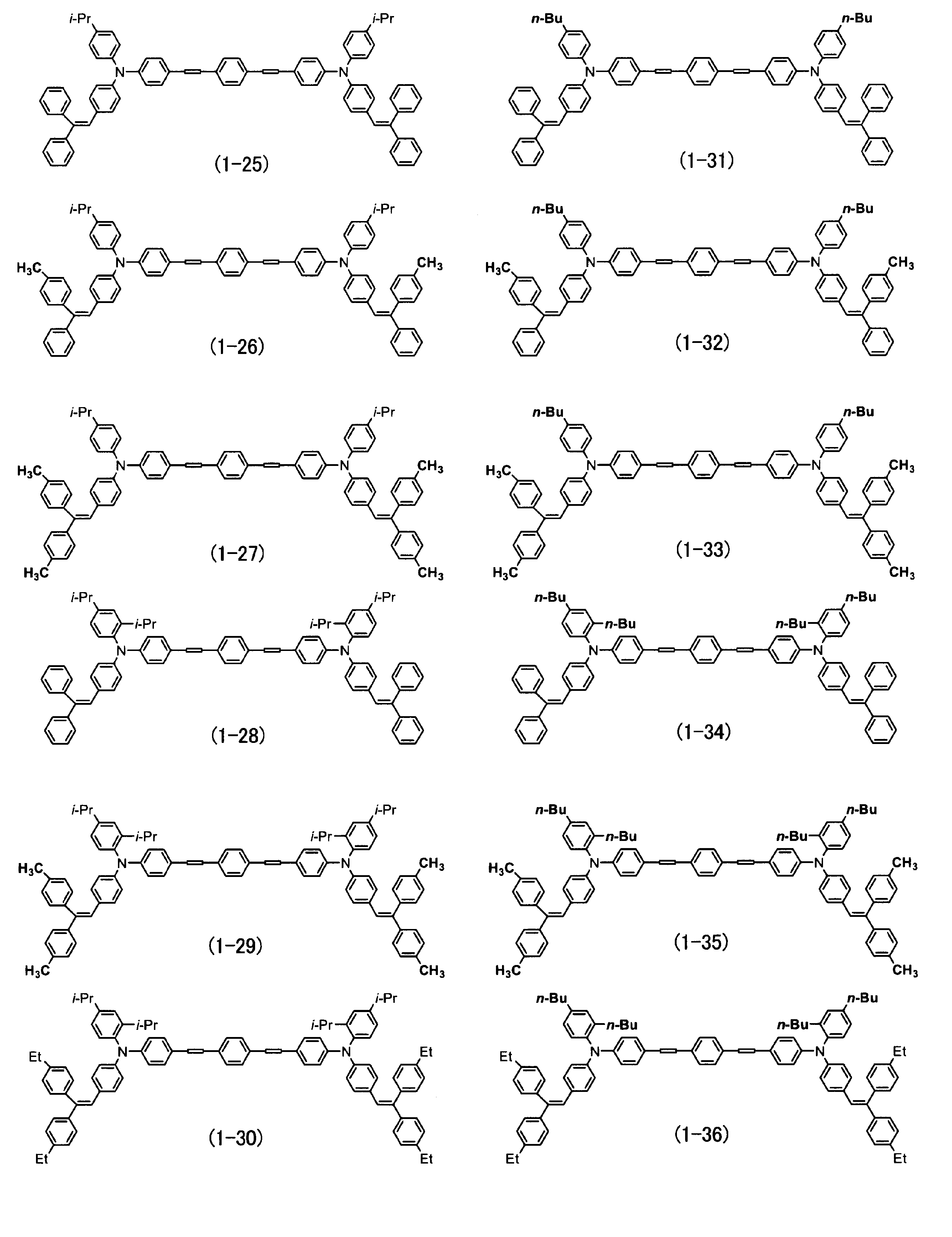
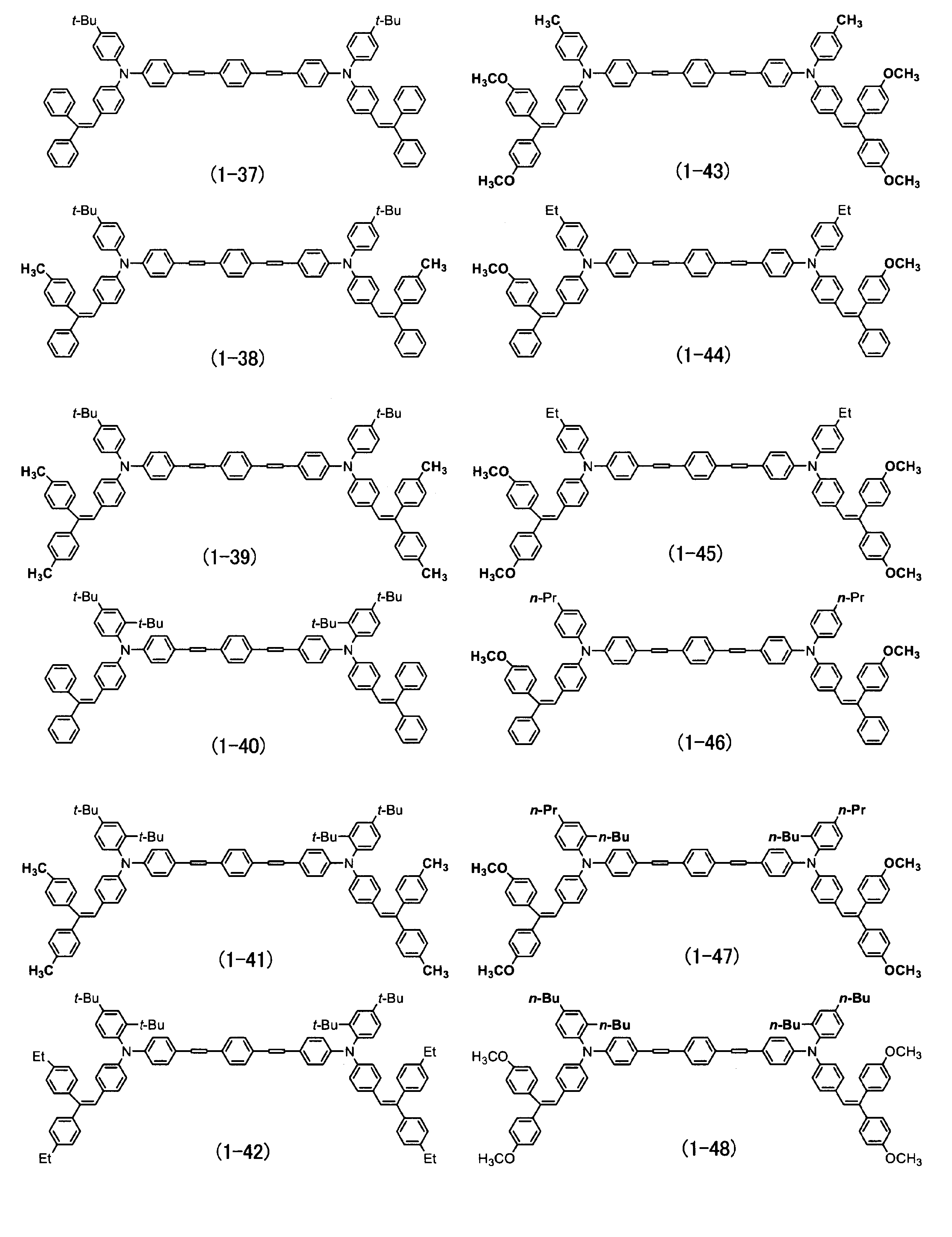
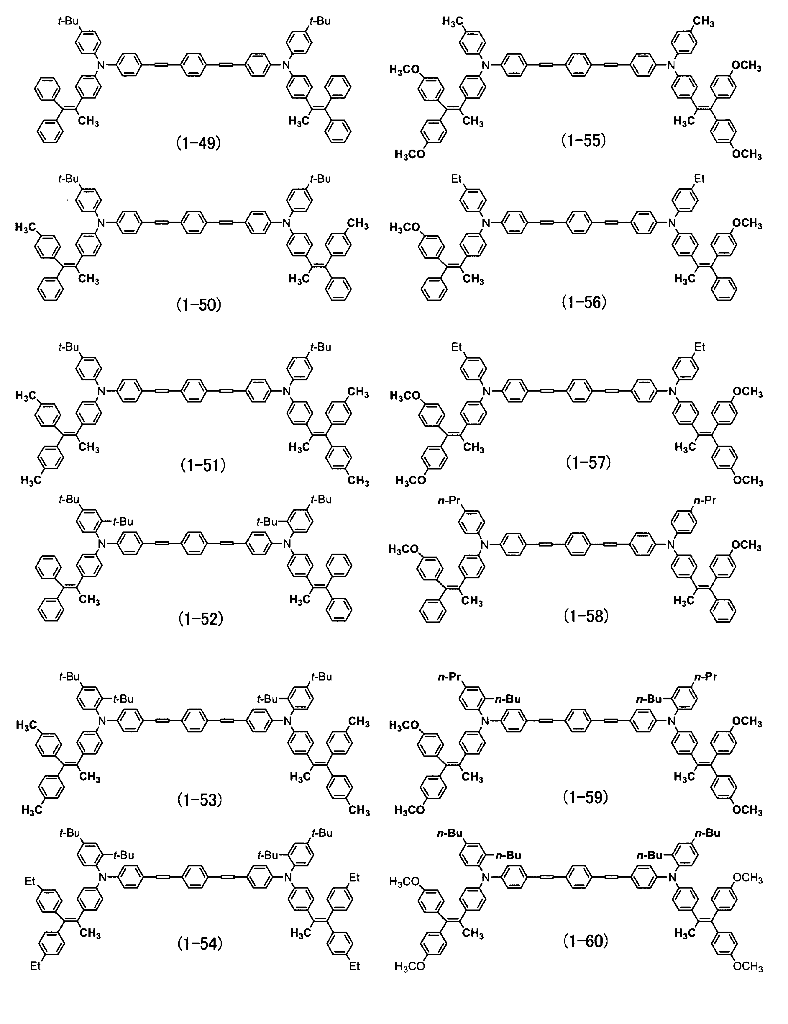

正孔輸送物質としては、高移動度のものを用いることが好ましく、具体的には、電界強度を20V/μmとしたときの正孔移動度が40×10-6~120×10-6[cm2/V・s]、特には60×10-6~120×10-6[cm2/V・s]、さらには70×10-6~120×10-6[cm2/V・s]のものを用いることが好ましい。一般式(1)で示される構造において、R1を有するベンゼン環に対し、置換基がメタ位あるいはパラ位に結合する正孔輸送物質が好ましい。
ここで、上記正孔移動度は、正孔輸送物質を、バインダー樹脂中に50質量%となるよう添加して得られた塗布液を用いて測定することができる。正孔輸送材料と樹脂バインダとの比は50:50である。バインダー樹脂はビスフェノールZ型ポリカーボネート樹脂でよい。例えば、ユピゼータPCZ-500(商品名、三菱ガス化学(株)製)でよい。具体的には、この塗布液を基材上に塗布し、120℃で30分間乾燥して膜厚7μmの塗膜を作製し、TOF(Time of Flight)法を用いて、一定の電界強度20V/μmにおける正孔移動度を測定することができる。測定温度は300Kである。
ここで、上記正孔移動度は、正孔輸送物質を、バインダー樹脂中に50質量%となるよう添加して得られた塗布液を用いて測定することができる。正孔輸送材料と樹脂バインダとの比は50:50である。バインダー樹脂はビスフェノールZ型ポリカーボネート樹脂でよい。例えば、ユピゼータPCZ-500(商品名、三菱ガス化学(株)製)でよい。具体的には、この塗布液を基材上に塗布し、120℃で30分間乾燥して膜厚7μmの塗膜を作製し、TOF(Time of Flight)法を用いて、一定の電界強度20V/μmにおける正孔移動度を測定することができる。測定温度は300Kである。
バインダー樹脂としての、上記一般式(2)で表される繰返し構造を有する樹脂の具体例としては以下のようなものが挙げられるが、これらに限定されるものではない。中でも、R12およびR13が水素原子であってR14およびR15がメチル基(k=1,p=1)であるものを用いると、耐摩耗性が向上するので、より好ましい。

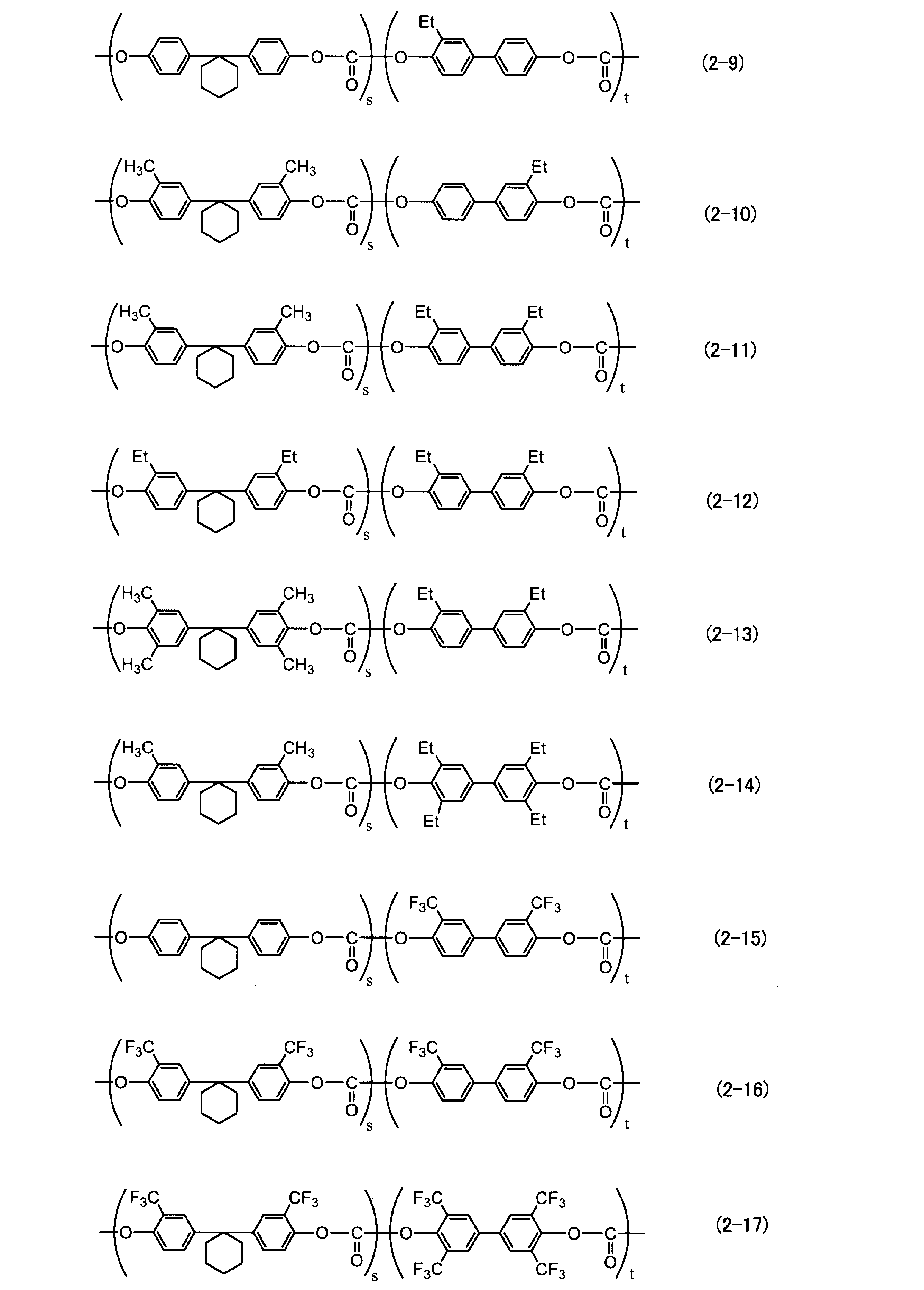
なお、s,tの比率は、0.3≦t/(s+t)≦0.7を満足することが好ましく、連鎖末端基は1価の芳香族基または1価のフッ素含有脂肪族基であることが好ましい。t/(s+t)を0.3以上とすることで、耐摩耗性および耐汚染性をともに良好に確保でき、t/(s+t)を0.7以下とすることで、樹脂の合成が容易となる。
電子輸送物質としての、上記一般式(ET1)で表される構造を有する化合物の具体例としては以下のようなものが挙げられるが、これらに限定されるものではない。


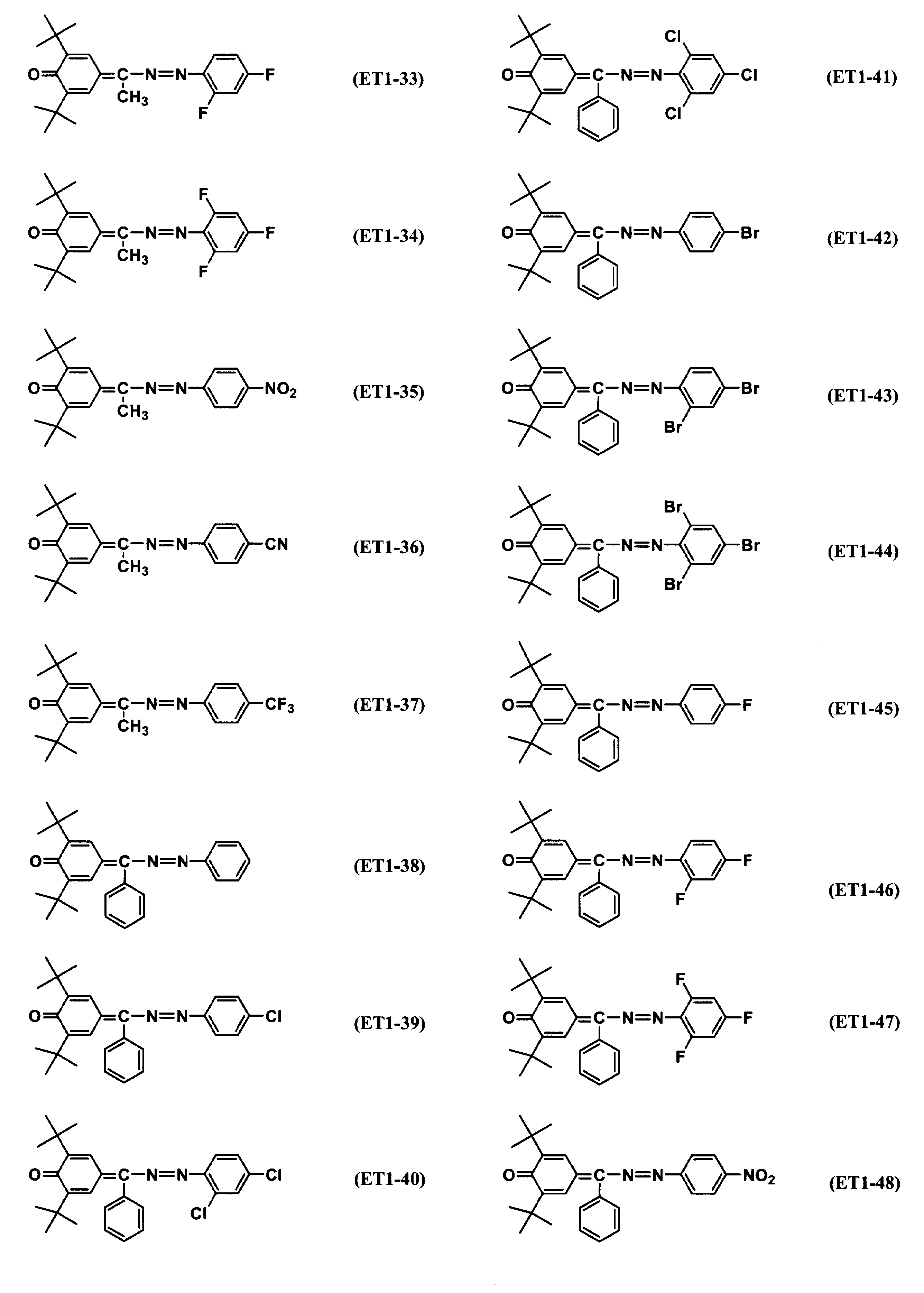


電子輸送物質としての、上記一般式(ET2)で表される構造を有する化合物の具体例としては以下のようなものが挙げられるが、これらに限定されるものではない。

電子輸送物質としての、上記一般式(ET3)で表される構造を有する化合物の具体例としては以下のようなものが挙げられるが、これらに限定されるものではない。
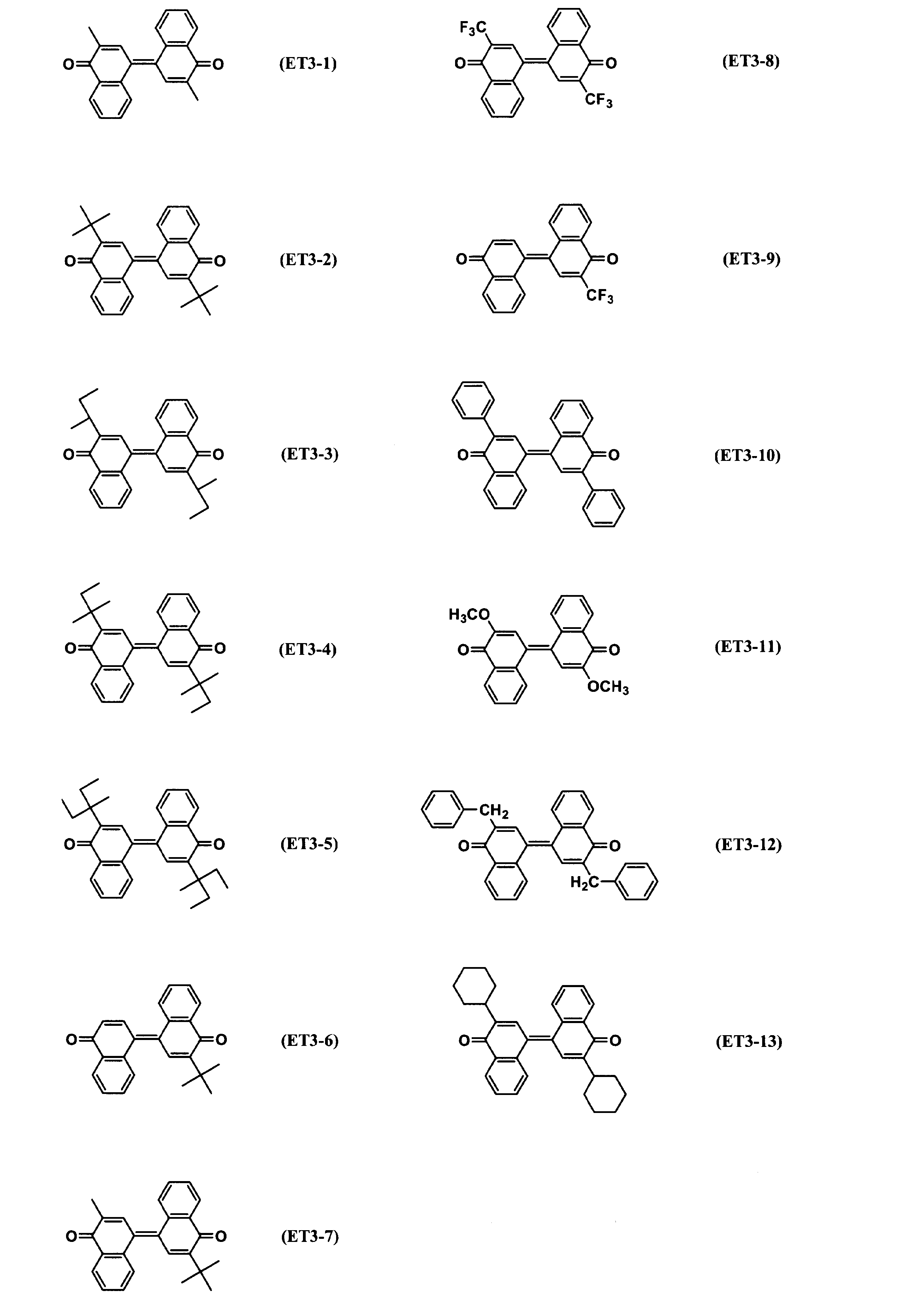
導電性基体1は、感光体の電極としての役目と同時に感光体を構成する各層の支持体となっており、円筒状、板状、フィルム状などいずれの形状でもよい。導電性基体1の材質としては、アルミニウム、ステンレス鋼、ニッケルなどの金属類、あるいはガラス、樹脂などの表面に導電処理を施したもの等を使用できる。
下引き層2は、樹脂を主成分とする層やアルマイトなどの金属酸化皮膜からなるものである。かかる下引き層2は、導電性基体1から感光層への電荷の注入性を制御するため、または、導電性基体1表面の欠陥の被覆、感光層と導電性基体1との接着性の向上などの目的で、必要に応じて設けられる。下引き層2に用いられる樹脂材料としては、カゼイン、ポリビニルアルコール、ポリアミド、メラミン、セルロースなどの絶縁性高分子、ポリチオフェン、ポリピロール、ポリアニリンなどの導電性高分子が挙げられ、これらの樹脂は単独、あるいは適宜組み合わせて混合して用いることができる。また、これらの樹脂に、二酸化チタン、酸化亜鉛などの金属酸化物を含有させて用いてもよい。
感光層は、前述したように、負帯電積層型の感光層6、正帯電単層型の感光層3および正帯電積層型の感光層7のいずれであってもよい。負帯電積層型の感光層6の場合には、電荷輸送層5が上記特定の正孔輸送物質、バインダー樹脂および電子輸送物質を含み、正帯電積層型の感光層7の場合には、電荷発生層4が上記特定の正孔輸送物質、バインダー樹脂および電子輸送物質を含む。
(負帯電積層型感光体)
負帯電積層型感光体において、電荷発生層4は、電荷発生物質の粒子をバインダー樹脂中に分散させた塗布液を塗布するなどの方法により形成され、光を受容して電荷を発生する。電荷発生層4は、その電荷発生効率が高いことと同時に発生した電荷の電荷輸送層5への注入性が重要であり、電場依存性が少なく、低電場でも注入の良いことが望ましい。
負帯電積層型感光体において、電荷発生層4は、電荷発生物質の粒子をバインダー樹脂中に分散させた塗布液を塗布するなどの方法により形成され、光を受容して電荷を発生する。電荷発生層4は、その電荷発生効率が高いことと同時に発生した電荷の電荷輸送層5への注入性が重要であり、電場依存性が少なく、低電場でも注入の良いことが望ましい。
電荷発生物質としては、X型無金属フタロシアニン、τ型無金属フタロシアニン、α型チタニルフタロシアニン、β型チタニルフタロシアニン、Y型チタニルフタロシアニン、γ型チタニルフタロシアニン、アモルファス型チタニルフタロシアニン、ε型銅フタロシアニンなどのフタロシアニン化合物、各種アゾ顔料、アントアントロン顔料、チアピリリウム顔料、ペリレン顔料、ペリノン顔料、スクアリリウム顔料、キナクリドン顔料等を単独、または適宜組み合わせて用いることができ、画像形成に使用される露光光源の光波長領域に応じて好適な物質を選ぶことができる。
電荷発生層4に用いるバインダー樹脂としては、ポリカーボネート樹脂、ポリエステル樹脂、ポリアミド樹脂、ポリウレタン樹脂、塩化ビニル樹脂、酢酸ビニル樹脂、フェノキシ樹脂、ポリビニルアセタール樹脂、ポリビニルブチラール樹脂、ポリスチレン樹脂、ポリスルホン樹脂、ジアリルフタレート樹脂、メタクリル酸エステル樹脂の重合体および共重合体などを適宜組み合わせて使用することが可能である。
電荷発生層4は、電荷発生機能を有すればよいので、その膜厚は電荷発生物質の光吸収係数より決まり、一般的には1μm以下であり、好適には0.5μm以下である。電荷発生層4は、電荷発生物質を主体として、これに電荷輸送物質などを添加して使用することも可能である。
電荷発生層4におけるバインダー樹脂の含有量としては、電荷発生層4の固形分に対して、好適には20~80質量%、より好適には30~70質量%である。また、電荷発生層4における電荷発生物質の含有量としては、電荷発生層4の固形分に対して、好適には20~80質量%、より好適には30~70質量%である。
負帯電積層型感光体においては、電荷輸送層5が、上記一般式(1)で表される構造を有する正孔輸送物質、上記一般式(2)で表される繰返し単位を有するバインダー樹脂、および、上記一般式(ET1)~(ET3)で表される構造を有する電子輸送物質のうちの少なくとも1種を含有する。これにより、本発明の所期の効果を得ることができる。
電荷輸送層5には、必要に応じて、本発明の効果を著しく損なわない範囲で、その他公知の正孔輸送物質を併用することもできる。その他公知の正孔輸送物質としては、例えば、ヒドラゾン化合物、ピラゾリン化合物、ピラゾロン化合物、オキサジアゾール化合物、オキサゾール化合物、アリールアミン化合物、ベンジジン化合物、スチルベン化合物、スチリル化合物、エナミン化合物、ブタジエン化合物、ポリビニルカルバゾール、ポリシラン等を、1種または2種以上で適宜組み合わせて使用することが可能である。
また、電荷輸送層5には、必要に応じて、本発明の効果を著しく損なわない範囲で、その他公知のバインダー樹脂を併用することもできる。その他公知のバインダー樹脂としては、例えば、前記一般式(1)で表される共重合ポリカーボネート樹脂以外のポリカーボネート樹脂、ポリアリレート樹脂、ポリエステル樹脂、ポリビニルアセタール樹脂、ポリビニルブチラール樹脂、ポリビニルアルコール樹脂、塩化ビニル樹脂、酢酸ビニル樹脂、ポリエチレン樹脂、ポリプロピレン樹脂、ポリスチレン樹脂、アクリル樹脂、ポリアミド樹脂、ケトン樹脂、ポリアセタール樹脂、ポリスルホン樹脂、メタクリル酸エステルの重合体などの熱可塑性樹脂や、アルキド樹脂、エポキシ樹脂、シリコン樹脂、尿素樹脂、フェノール樹脂、不飽和ポリエステル樹脂、ポリウレタン樹脂、メラミン樹脂などの熱硬化性樹脂、およびこれらの共重合体等を、1種または2種以上で適宜組み合わせて使用することが可能である。
さらに、電荷輸送層5には、必要に応じて、本発明の効果を著しく損なわない範囲で、その他公知の電子輸送物質を併用することもできる。その他公知の電子輸送物質としては、無水琥珀酸、無水マレイン酸、ジブロム無水琥珀酸、無水フタル酸、3-ニトロ無水フタル酸、4-ニトロ無水フタル酸、無水ピロメリット酸、ピロメリット酸、トリメリット酸、無水トリメリット酸、フタルイミド、4-ニトロフタルイミド、テトラシアノエチレン、テトラシアノキノジメタン、クロラニル、ブロマニル、o-ニトロ安息香酸、マロノニトリル、トリニトロフルオレノン、トリニトロチオキサントン、ジニトロベンゼン、ジニトロアントラセン、ジニトロアクリジン、ニトロアントラキノン、ジニトロアントラキノン、チオピラン系化合物、キノン系化合物、ベンゾキノン系化合物、ジフェノキノン系化合物、ナフトキノン系化合物、アゾキノン系化合物、アントラキノン系化合物、ジイミノキノン系化合物、スチルベンキノン系化合物等の電子輸送物質(アクセプター性化合物)を、1種または2種以上で適宜組み合わせて使用することが可能である。
電荷輸送層5におけるバインダー樹脂の含有量としては、電荷輸送層5の固形分に対して、好適には55~85質量%、より好適には60~75質量%である。バインダー樹脂を上記範囲で含有させることで、感光体の耐摩耗性および耐刷性をより向上することができ、好ましい。また、電荷輸送層5における正孔輸送物質の含有量としては、バインダー樹脂100質量部に対し、好適には20~80質量部であり、より好適には30~70質量部である。さらに、電荷輸送層5における電子輸送物質の含有量としては、バインダー樹脂100質量部に対し、好適には1~10質量部であり、より好適には3~5質量部である。
なお、電荷輸送層5の膜厚は、実用的に有効な表面電位を維持するためには5~60μmが好ましく、より好ましくは10~40μmである。
(正帯電単層型感光体)
正帯電単層型感光体において、正帯電単層型の感光層3は、正孔輸送物質としての上記一般式(1)で表される構造を有する化合物、バインダー樹脂としての上記一般式(2)で表される繰返し単位を有する樹脂、および、電子輸送物質としての上記一般式(ET1)~(ET3)で表される構造を有する化合物の少なくとも1種に加えて、電荷発生物質を含有して構成することができる。これにより、本発明の所期の効果を得ることができる。
正帯電単層型感光体において、正帯電単層型の感光層3は、正孔輸送物質としての上記一般式(1)で表される構造を有する化合物、バインダー樹脂としての上記一般式(2)で表される繰返し単位を有する樹脂、および、電子輸送物質としての上記一般式(ET1)~(ET3)で表される構造を有する化合物の少なくとも1種に加えて、電荷発生物質を含有して構成することができる。これにより、本発明の所期の効果を得ることができる。
感光層3に用いる電荷発生物質としては、例えば、フタロシアニン系顔料、アゾ顔料、アントアントロン顔料、ペリレン顔料、ペリノン顔料、多環キノン顔料、スクアリリウム顔料、チアピリリウム顔料、キナクリドン顔料等を使用することができる。また、これら電荷発生物質を単独または2種以上で適宜組み合わせて使用することが可能である。特に、アゾ顔料としては、ジスアゾ顔料、トリスアゾ顔料、ペリレン顔料としては、N,N’-bis(3,5-dimethylphenyl)-3,4:9,10-perylene-bis(carboximide)、フタロシアニン系顔料としては、無金属フタロシアニン、銅フタロシアニン、チタニルフタロシアニンが好ましい。さらには、X型無金属フタロシアニン、τ型無金属フタロシアニン、ε型銅フタロシアニン、α型チタニルフタロシアニン、β型チタニルフタロシアニン、Y型チタニルフタロシアニン、アモルファスチタニルフタロシアニン、特開平8-209023号公報、米国特許第5736282号明細書および米国特許第5874570号明細書に記載のCuKα:X線回析スペクトルにてブラッグ角2θが9.6°を最大ピークとするチタニルフタロシアニンを用いると、感度、耐久性および画質の点で著しく改善された効果を示す。
正帯電単層型の感光層3には、必要に応じて、本発明の効果を著しく損なわない範囲で、その他公知の正孔輸送物質を併用することもできる。その他公知の正孔輸送物質としては、例えば、ヒドラゾン化合物、ピラゾリン化合物、ピラゾロン化合物、オキサジアゾール化合物、オキサゾール化合物、アリールアミン化合物、ベンジジン化合物、スチルベン化合物、スチリル化合物、ポリ-N-ビニルカルバゾール、ポリシラン等を、単独または2種以上で適宜組み合わせて使用することが可能である。正孔輸送物質としては、光照射時に発生する正孔の輸送能力が優れている他、電荷発生物質との組み合せに好適なものが好ましい。
また、正帯電単層型の感光層3には、必要に応じて、本発明の効果を著しく損なわない範囲で、その他公知のバインダー樹脂を併用することもできる。その他公知のバインダー樹脂としては、上記一般式(2)で示される繰返し単位を有する共重合ポリカーボネート樹脂以外の、ビスフェノールA型、ビスフェノールZ型、ビスフェノールA型‐ビフェニル共重合体などの各種ポリカーボネート樹脂、ポリフェニレン樹脂、ポリエステル樹脂、ポリビニルアセタール樹脂、ポリビニルブチラール樹脂、ポリビニルアルコール樹脂、塩化ビニル樹脂、酢酸ビニル樹脂、ポリエチレン樹脂、ポリプロピレン樹脂、アクリル樹脂、ポリウレタン樹脂、エポキシ樹脂、メラミン樹脂、シリコーン樹脂、ポリアミド樹脂、ポリスチレン樹脂、ポリアセタール樹脂、ポリアリレート樹脂、ポリスルホン樹脂、メタクリル酸エステルの重合体およびこれらの共重合体等を、1種または2種以上で適宜組み合わせて使用することが可能である。さらに、分子量の異なる同種の樹脂を混合して用いてもよい。
さらに、正帯電単層型の感光層3には、必要に応じて、本発明の効果を著しく損なわない範囲で、その他公知の電子輸送物質を併用することもできる。その他公知の電子輸送物質としては、例えば、無水琥珀酸、無水マレイン酸、ジブロモ無水琥珀酸、無水フタル酸、3-ニトロ無水フタル酸、4-ニトロ無水フタル酸、無水ピロメリット酸、ピロメリット酸、トリメリット酸、無水トリメリット酸、フタルイミド、4-ニトロフタルイミド、テトラシアノエチレン、テトラシアノキノジメタン、クロラニル、ブロマニル、o-ニトロ安息香酸、マロノニトリル、トリニトロフルオレノン、トリニトロチオキサントン、ジニトロベンゼン、ジニトロアントラセン、ジニトロアクリジン、ニトロアントラキノン、ジニトロアントラキノン、チオピラン系化合物、キノン系化合物、ベンゾキノン化合物、ジフェノキノン系化合物、ナフトキノン系化合物、アントラキノン系化合物、スチルベンキノン系化合物、アゾキノン系化合物等を、1種または2種以上で適宜組み合わせて使用することが可能である。
正帯電単層型の感光層3におけるバインダー樹脂の含有量としては、感光層3の固形分に対して、好適には55~85質量%、より好適には60~80質量%である。バインダー樹脂を上記範囲で含有させることで、感光体の耐摩耗性および耐刷性をより向上することができ、好ましい。また、感光層3における正孔輸送物質の含有量としては、バインダー樹脂100質量部に対し、好適には3~80質量部であり、より好適には5~60質量部である。さらに、感光層3における電子輸送物質の含有量としては、バインダー樹脂100質量部に対し、好適には1~50質量部であり、より好適には5~40質量部である。さらにまた、感光層3における電荷発生物質の含有量としては、バインダー樹脂100質量部に対し、好適には0.1~20質量部であり、より好適には0.5~10質量部である。
単層型感光層3の膜厚は、実用的に有効な表面電位を維持するためには3~100μmの範囲が好ましく、5~40μmの範囲がより好ましい。
(正帯電積層型感光体)
正帯電積層型感光体において、電荷輸送層5は、主として電荷輸送物質とバインダー樹脂とにより構成される。電荷輸送層5に用いる電荷輸送物質およびバインダー樹脂としては、負帯電積層型感光体における電荷輸送層5について挙げたものと同様の材料を用いることができる。各材料の含有量や、電荷輸送層5の膜厚も負帯電積層型感光体と同様とすることができる。
正帯電積層型感光体において、電荷輸送層5は、主として電荷輸送物質とバインダー樹脂とにより構成される。電荷輸送層5に用いる電荷輸送物質およびバインダー樹脂としては、負帯電積層型感光体における電荷輸送層5について挙げたものと同様の材料を用いることができる。各材料の含有量や、電荷輸送層5の膜厚も負帯電積層型感光体と同様とすることができる。
正帯電積層型感光体において、電荷発生層4は、正孔輸送物質としての上記一般式(1)で表される構造を有する化合物、バインダー樹脂としての上記一般式(2)で表される繰返し単位を有する樹脂、および、電子輸送物質としての上記一般式(ET1)~(ET3)で表される構造を有する化合物の少なくとも1種に加えて、電荷発生物質を含有して構成することができる。これにより、本発明の所期の効果を得ることができる。
電荷発生層4に用いる電荷発生物質としては、正帯電単層型感光体における正帯電単層型の感光層3について挙げたものと同様の材料を用いることができる。また、正孔輸送物質、電子輸送物質、およびバインダー樹脂についても、感光層3におけるのと同様に、必要に応じて、本発明の効果を著しく損なわない範囲で、その他公知の材料を併用することができる。各材料の含有量や、電荷発生層4の膜厚についても、感光層3と同様とすることができる。
ここで、積層型または単層型のいずれの感光層中にも、耐環境性や有害な光に対する安定性を向上させる目的で、本発明の効果を著しく損なわない範囲で、酸化防止剤、ラジカル捕捉剤、一重項クエンチャー、紫外線吸収剤、光安定剤等の劣化防止剤を含有させることができる。このような化合物としては、例えば、トコフェロールなどのクロマノール誘導体およびエステル化化合物、ポリアリールアルカン化合物、ハイドロキノン誘導体、エーテル化化合物、ジエーテル化化合物、ベンゾフェノン誘導体、ベンゾトリアゾール誘導体、チオエーテル化合物、フェニレンジアミン誘導体、ホスホン酸エステル、亜リン酸エステル、フェノール化合物、ヒンダードフェノール化合物、直鎖アミン化合物、環状アミン化合物、ヒンダードアミン化合物、ビフェニル誘導体等が挙げられる。
また、上記感光層中には、形成した膜のレベリング性の向上や潤滑性の付与を目的として、シリコーンオイルやフッ素系オイル等のレベリング剤を含有させることもできる。さらに、膜硬度の調整、摩擦係数の低減、潤滑性の付与等を目的として、酸化ケイ素(シリカ)、酸化チタン、酸化亜鉛、酸化カルシウム、酸化アルミニウム(アルミナ)、酸化ジルコニウム等の金属酸化物、硫酸バリウム、硫酸カルシウム等の金属硫酸塩、窒化ケイ素、窒化アルミニウム等の金属窒化物の微粒子、または、4フッ化エチレン樹脂等のフッ素系樹脂粒子、フッ素系クシ型グラフト重合樹脂粒子等を含有してもよい。さらにまた、必要に応じて、電子写真特性を著しく損なわない範囲で、その他公知の添加剤を含有させることもできる。
(感光体の製造方法)
本発明の実施形態の感光体の製造方法は、上記電子写真用感光体を製造するにあたり、導電性基体上に塗布液を塗布して感光層を形成する工程を包含するものであり、上記一般式(1)で示される構造を有する正孔輸送物質と、上記一般式(2)で示される繰返し構造を有するバインダー樹脂と、上記一般式(ET1)~(ET3)で示される構造を有する電子輸送物質のうちの少なくとも1種と、を含有する上記塗布液を準備する工程を備える。
本発明の実施形態の感光体の製造方法は、上記電子写真用感光体を製造するにあたり、導電性基体上に塗布液を塗布して感光層を形成する工程を包含するものであり、上記一般式(1)で示される構造を有する正孔輸送物質と、上記一般式(2)で示される繰返し構造を有するバインダー樹脂と、上記一般式(ET1)~(ET3)で示される構造を有する電子輸送物質のうちの少なくとも1種と、を含有する上記塗布液を準備する工程を備える。
具体的には、負帯電積層型感光体の場合、まず、任意の電荷発生材料および樹脂バインダーを溶媒中に溶解、分散させて電荷発生層の形成用塗布液を調製し準備する工程と、この電荷発生層の形成用塗布液を、導電性基体の外周に、所望に応じ下引き層を介して塗工、乾燥させて電荷発生層を形成する工程と、を含む方法により、電荷発生層を形成する。次に、上記特定の正孔輸送材料、樹脂バインダーおよび電子輸送材料を溶媒中に溶解させて電荷輸送層の形成用塗布液を調製し準備する工程と、この電荷輸送層の形成用塗布液を、上記電荷発生層上に塗工、乾燥させて電荷輸送層を形成する工程と、を含む方法により電荷輸送層を形成する。このような製造方法により、実施形態の負帯電積層型感光体を製造することができる。
また、正帯電単層型感光体は、上記特定の正孔輸送材料、樹脂バインダーおよび電子輸送材料、並びに、任意の電荷発生材料を、溶媒中に溶解、分散させて単層型感光層の形成用塗布液を調製し準備する工程と、この単層型感光層の形成用塗布液を、導電性基体の外周に、所望に応じ下引き層を介して塗工、乾燥させて感光層を形成する工程と、を含む方法により、製造することができる。
さらに、正帯電積層型感光体の場合、まず、任意の正孔輸送材料および樹脂バインダーを溶媒に溶解させて電荷輸送層の形成用塗布液を調製し準備する工程と、この電荷輸送層の形成用塗布液を、導電性基体の外周に、所望に応じ下引き層を介して塗工、乾燥させて電荷輸送層を形成する工程と、を含む方法により、電荷輸送層を形成する。次に、上記特定の正孔輸送材料、樹脂バインダーおよび電子輸送材料、並びに、任意の電荷発生材料を、溶媒中に溶解、分散させて電荷発生層の形成用塗布液を調製し準備する工程と、この電荷発生層の形成用塗布液を、上記電荷輸送層上に塗工、乾燥させて電荷発生層を形成する工程と、を含む方法により電荷発生層を形成する。このような製造方法により実施形態の正帯電積層型感光体を製造することができる。
ここで、塗布液の調製に用いる溶媒の種類や、塗工条件、乾燥条件等については、常法に従い適宜選択することができ、特に制限されるものではない。好適には、塗工方法としては、浸漬塗工法を用いる。浸漬塗工法を用いることで、外観品質が良好で電気特性の安定した感光体を、低コストかつ高生産性を確保しつつ製造することができる。
(電子写真装置)
本発明の実施形態の電子写真用感光体は、各種マシンプロセスに適用することにより所期の効果が得られるものである。具体的には、ローラやブラシなどの帯電部材を用いた接触帯電方式、コロトロンやスコロトロンなどの帯電部材を用いた非接触帯電方式等の帯電プロセス、並びに、非磁性一成分、磁性一成分、二成分などの現像剤を用いた接触現像および非接触現像方式などの現像プロセスにおいても、十分な効果を得ることができる。
本発明の実施形態の電子写真用感光体は、各種マシンプロセスに適用することにより所期の効果が得られるものである。具体的には、ローラやブラシなどの帯電部材を用いた接触帯電方式、コロトロンやスコロトロンなどの帯電部材を用いた非接触帯電方式等の帯電プロセス、並びに、非磁性一成分、磁性一成分、二成分などの現像剤を用いた接触現像および非接触現像方式などの現像プロセスにおいても、十分な効果を得ることができる。
図4に、本発明の電子写真装置の一構成例の概略構成図を示す。図示する電子写真装置60は、導電性基体1と、その外周面上に被覆された下引き層2および感光層300とを含む、本発明の実施形態の感光体8を搭載する。この電子写真装置60は、感光体8の外周縁部に配置された、図示する例ではローラ状の帯電部材21と、この帯電部材21に印加電圧を供給する高圧電源22と、像露光部材23と、現像ローラ241を備えた現像器24と、給紙ローラ251および給紙ガイド252を備えた給紙部材25と、転写帯電器(直接帯電型)26と、から構成される。電子写真装置60は、さらに、クリーニングブレード271を備えたクリーニング装置27と、除電部材28と、を含んでもよい。また、本発明の実施形態の電子写真装置60は、カラープリンタとすることができる。
以下、本発明の具体的態様を、実施例を用いてさらに詳細に説明する。本発明はその要旨を超えない限り、以下の実施例によって限定されるものではない。
(負帯電積層型感光体の製造)
(実施例1)
アルコール可溶性ナイロン(東レ(株)製、商品名「CM8000」)5質量部と、アミノシラン処理された酸化チタン微粒子5質量部とを、メタノール90質量部に溶解、分散させて、下引き層用塗布液を調製した。導電性基体1としての外径30mmのアルミニウム製円筒の外周に、この下引き層用塗布液を浸漬塗工し、温度100℃で30分間乾燥して、膜厚3μmの下引き層2を形成した。
(実施例1)
アルコール可溶性ナイロン(東レ(株)製、商品名「CM8000」)5質量部と、アミノシラン処理された酸化チタン微粒子5質量部とを、メタノール90質量部に溶解、分散させて、下引き層用塗布液を調製した。導電性基体1としての外径30mmのアルミニウム製円筒の外周に、この下引き層用塗布液を浸漬塗工し、温度100℃で30分間乾燥して、膜厚3μmの下引き層2を形成した。
電荷発生物質としてのY型チタニルフタロシアニン1質量部と、バインダー樹脂としてのポリビニルブチラール樹脂(積水化学(株)製、商品名「エスレックKS-1」)1.5質量部とをジクロロメタン60質量部に溶解、分散させて、電荷発生層用塗布液を調製した。下引き層2上に、この電荷発生層用塗布液を浸漬塗工し、温度80℃で30分間乾燥して、膜厚0.3μmの電荷発生層4を形成した。
バインダー樹脂としての、上記構造式(2-5)で示され、t/(s+t)=0.5であって、かつ、末端基が下記構造式(3)で示される基である質量平均分子量50,000の共重合ポリカーボネート樹脂130質量部と、正孔輸送物質としての上記構造式(1-5)で示される化合物70質量部(バインダー樹脂100質量部に対し約54質量部)と、上記構造式(ET2-3)で示される電子輸送物質5質量部(バインダー樹脂100質量部に対し約3.8質量部)とを、ジクロロメタン1000質量部に溶解して、電荷輸送層用塗布液を調製した。構造式(1-5)で示される化合物の正孔移動度は、電界強度を20V/μmとしたとき75.2×10-6[cm2/V・s]であった。バインダー樹脂の含有量は、電荷輸送層5の固形分に対し約63質量%であった。
電荷発生層4上に、この電荷輸送層用塗布液を浸漬塗工し、温度90℃で60分間乾燥して、膜厚25μmの電荷輸送層5を形成し、負帯電積層型感光体を作製した。

電荷発生層4上に、この電荷輸送層用塗布液を浸漬塗工し、温度90℃で60分間乾燥して、膜厚25μmの電荷輸送層5を形成し、負帯電積層型感光体を作製した。
(実施例2~22、比較例1~15)
電荷輸送層5のバインダー樹脂、正孔輸送物質および電子輸送物質を、下記の表中に示すように変更した以外は、実施例1と同様の方法で、電子写真感光体を作製した。
なお、各実施例および比較例において使用した正孔輸送物質の、電界強度20V/μmにおける正孔移動度(×10-6[cm2/V・s])は次のとおりである。
構造式(1-2)で示される化合物:73.9
構造式(A-100)で示される化合物:13.2
構造式(A-101)で示される化合物:9.57
構造式(A-102)で示される化合物:34.5
実施例で使用した、上記以外の、一般式(1)で表される正孔輸送物質の正孔移動度は、その分子構造から、いずれも電界強度を20V/μmとしたとき60×10-6~120×10-6[cm2/V・s]の範囲内にあると推定される。
下記の表中で使用した材料の構造式を、以下に示す。
電荷輸送層5のバインダー樹脂、正孔輸送物質および電子輸送物質を、下記の表中に示すように変更した以外は、実施例1と同様の方法で、電子写真感光体を作製した。
なお、各実施例および比較例において使用した正孔輸送物質の、電界強度20V/μmにおける正孔移動度(×10-6[cm2/V・s])は次のとおりである。
構造式(1-2)で示される化合物:73.9
構造式(A-100)で示される化合物:13.2
構造式(A-101)で示される化合物:9.57
構造式(A-102)で示される化合物:34.5
実施例で使用した、上記以外の、一般式(1)で表される正孔輸送物質の正孔移動度は、その分子構造から、いずれも電界強度を20V/μmとしたとき60×10-6~120×10-6[cm2/V・s]の範囲内にあると推定される。
下記の表中で使用した材料の構造式を、以下に示す。
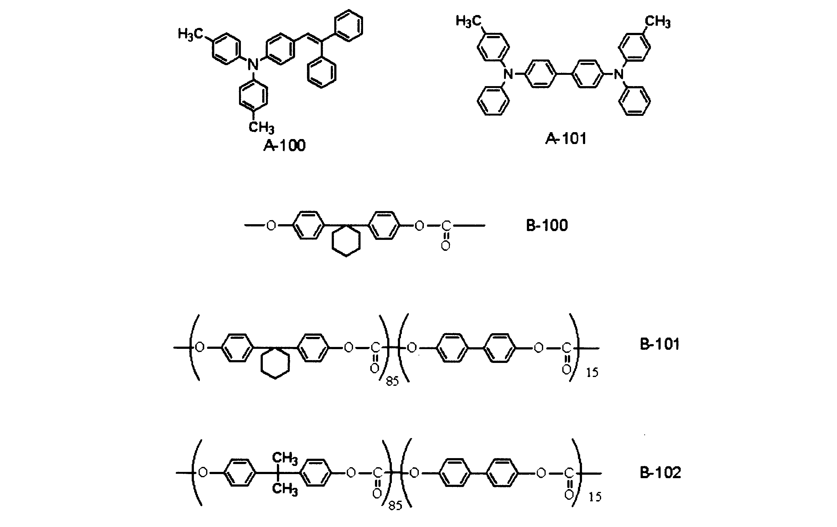


実施例1~22および比較例1~15において作製した電子写真感光体を用いて、以下に示す評価方法にて、それぞれ電気特性、電位安定性、耐摩耗性、耐光性、フィルミング、および、耐汚染性について評価した。その結果を、下記の表中に示す。
(電気特性の評価)
各実施例および比較例にて得られた感光体の電気特性を、ジェンテック社製のプロセスシミュレーター(CYNTHIA91)を使用して、以下の方法で評価した。実施例1~22および比較例1~15の感光体について、温度22℃、湿度50%の環境下で、感光体の表面を暗所にてコロナ放電により-650Vに帯電せしめた後、暗所で5秒間放置した。
次に、ハロゲンランプを光源とし、フィルターを用いて780nmに分光した1.0μW/cm2の露光光を、表面電位が-600Vになった時点から感光体に5秒間照射した。表面電位が-300Vとなるまで光減衰するのに要する露光量をE1/2(μJ/cm2)とし、露光後5秒後の感光体表面の残留電位をVr5(-V)とした。
各実施例および比較例にて得られた感光体の電気特性を、ジェンテック社製のプロセスシミュレーター(CYNTHIA91)を使用して、以下の方法で評価した。実施例1~22および比較例1~15の感光体について、温度22℃、湿度50%の環境下で、感光体の表面を暗所にてコロナ放電により-650Vに帯電せしめた後、暗所で5秒間放置した。
次に、ハロゲンランプを光源とし、フィルターを用いて780nmに分光した1.0μW/cm2の露光光を、表面電位が-600Vになった時点から感光体に5秒間照射した。表面電位が-300Vとなるまで光減衰するのに要する露光量をE1/2(μJ/cm2)とし、露光後5秒後の感光体表面の残留電位をVr5(-V)とした。
(電位安定性および耐摩耗性の評価)
各実施例および比較例において作製した感光体を、感光体の表面電位も測定できるように改造を施した、2成分現像方式のデジタル複写機(キャノン社製,image Runner color 2880)に搭載し、1万枚印字前後における明部電位の変化量、および、紙やブレードとの摩擦による感光層の膜削れ量について評価した。
各実施例および比較例において作製した感光体を、感光体の表面電位も測定できるように改造を施した、2成分現像方式のデジタル複写機(キャノン社製,image Runner color 2880)に搭載し、1万枚印字前後における明部電位の変化量、および、紙やブレードとの摩擦による感光層の膜削れ量について評価した。
(光疲労特性およびフィルミングの評価)
各実施例および比較例において作製した感光体を、光を照射する部分に開口部を設けた黒紙で覆って、500lxの照度に調整した白色蛍光灯の光を10分間照射した。光照射終了直後に感光体をキャノン社製のimage Runner color 2880に搭載して、黒45%のハーフトーン画像を出力し、光照射部と非照射部との印字濃度差を測定した。印字濃度差が0.03以下の場合を○、0.03を超え0.06以下の場合を△、0.06を超える場合を×として評価した。
各実施例および比較例において作製した感光体を、光を照射する部分に開口部を設けた黒紙で覆って、500lxの照度に調整した白色蛍光灯の光を10分間照射した。光照射終了直後に感光体をキャノン社製のimage Runner color 2880に搭載して、黒45%のハーフトーン画像を出力し、光照射部と非照射部との印字濃度差を測定した。印字濃度差が0.03以下の場合を○、0.03を超え0.06以下の場合を△、0.06を超える場合を×として評価した。
また、フィルミング評価については、繰返し印字後における感光体表面へのトナーの付着の有無により判定を行った。トナー付着が観察されなかったものは○、トナー付着がやや観察されたものは△、トナー付着が明確に観察されたものは×と評価した。
(耐汚染性の評価)
各実施例および比較例において作製した感光体を帯電ローラおよび転写ローラに当接させ、温度60℃で湿度90%環境に30日間放置した。帯電ローラおよび転写ローラはHP社製のプリンターLJ4250に搭載されるものと同型であった。放置後の感光体をHP社製のプリンターLJ4250に搭載し、ハーフトーン画像を印字して画像評価を行った。ハーフトーン画像に黒スジの発生がない場合を○、ハーフトーン画像に実用上問題ない程度の黒スジの発生があった場合を△、ハーフトーン画像に黒スジの発生があった場合を×とした。
各実施例および比較例において作製した感光体を帯電ローラおよび転写ローラに当接させ、温度60℃で湿度90%環境に30日間放置した。帯電ローラおよび転写ローラはHP社製のプリンターLJ4250に搭載されるものと同型であった。放置後の感光体をHP社製のプリンターLJ4250に搭載し、ハーフトーン画像を印字して画像評価を行った。ハーフトーン画像に黒スジの発生がない場合を○、ハーフトーン画像に実用上問題ない程度の黒スジの発生があった場合を△、ハーフトーン画像に黒スジの発生があった場合を×とした。
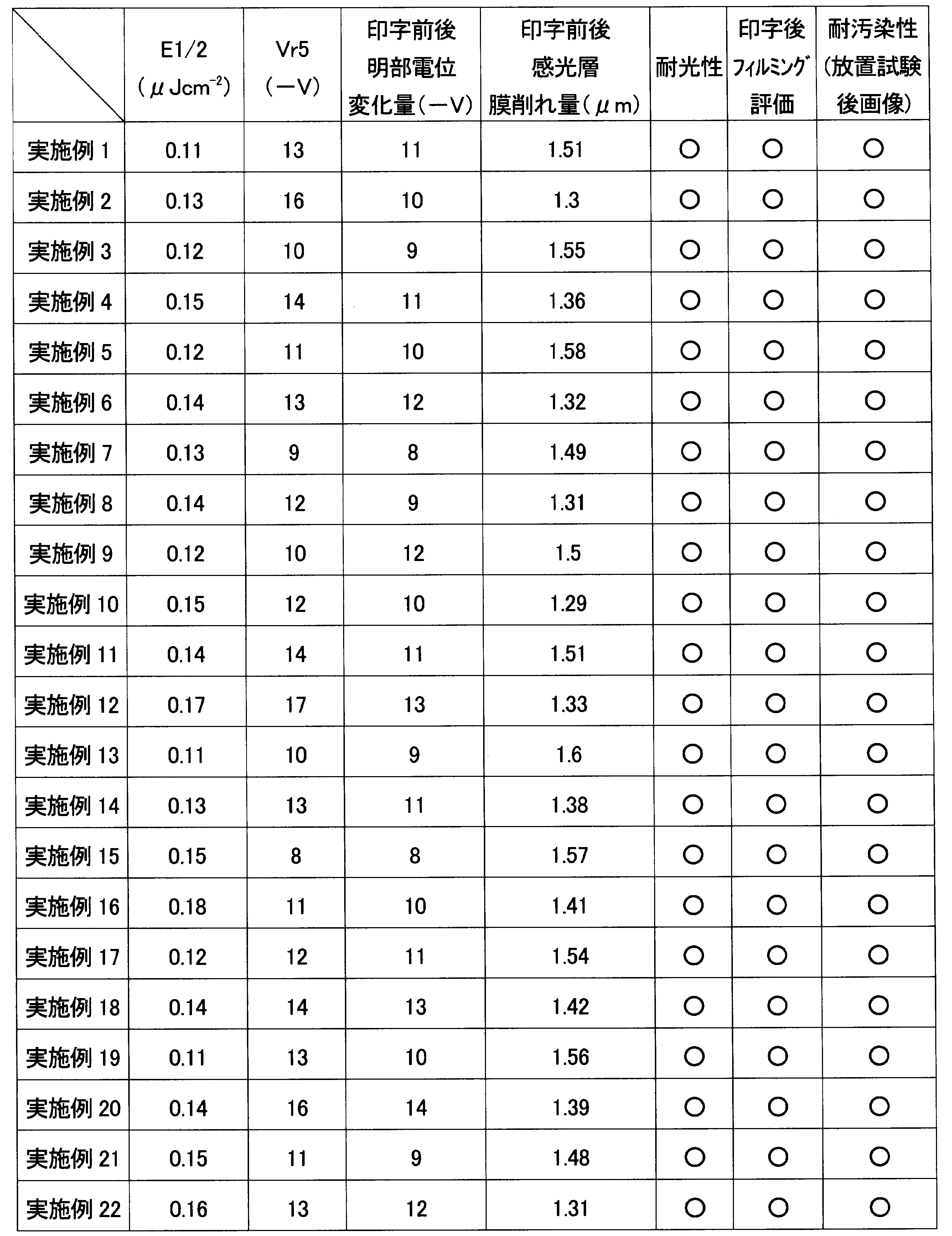
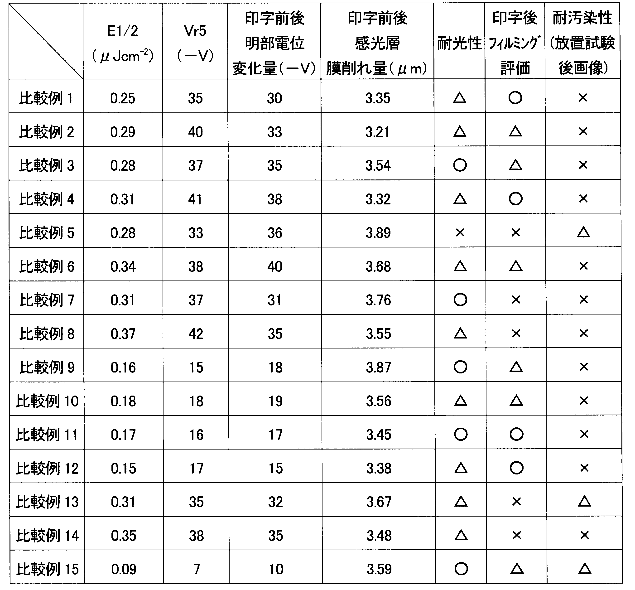
上記表中の結果から、負帯電積層型感光体の電荷輸送層中に特定の高移動度正孔輸送物質、ポリカーボネート樹脂および電子輸送物質の組合せを含有させることにより、電気特性および耐汚染性を改善できた。電荷輸送層におけるポリカーボネート樹脂の含有量が電荷輸送層の固形分に対し55質量%以上であることにより、比較例対比で1万枚繰り返し印字後の膜削れ量を50%以上低減できることが明らかとなった。また、このとき、印字後の電位および画像評価において問題が見られることはなかった。
(正帯電単層型感光体の製造)
(実施例23)
導電性基体1としての外径24mmのアルミニウム製円筒の外周に、塩化ビニル-酢酸ビニル-ビニルアルコール共重合体(日信化学工業(株)製、商品名「ソルバインTA5R」)0.2質量部をメチルエチルケトン99質量部に攪拌溶解させて調製した下引き層形成用塗布液を浸漬塗工し、温度100℃で30分間乾燥して、膜厚0.1μmの下引き層2を形成した。
(実施例23)
導電性基体1としての外径24mmのアルミニウム製円筒の外周に、塩化ビニル-酢酸ビニル-ビニルアルコール共重合体(日信化学工業(株)製、商品名「ソルバインTA5R」)0.2質量部をメチルエチルケトン99質量部に攪拌溶解させて調製した下引き層形成用塗布液を浸漬塗工し、温度100℃で30分間乾燥して、膜厚0.1μmの下引き層2を形成した。
電荷発生物質としての下記式、
 で示される無金属フタロシアニン1.5質量部(バインダー樹脂100質量部に対し約1.2質量部)と、正孔輸送物質としての上記構造式(1-5)で示される化合物45質量部(バインダー樹脂100質量部に対し約34.6質量部)と、電子輸送物質としての上記構造式(ET2-3)で示される化合物35質量部(バインダー樹脂100質量部に対し約26.9質量部)と、バインダー樹脂としての上記構造式(2-5)で示される樹脂130質量部とを、テトラヒドロフラン850質量部に溶解、分散させて単層型感光層形成用塗布液を調製した。構造式(1-5)で示される化合物の正孔移動度は、電界強度を20V/μmとしたとき75.2×10-6[cm2/V・s]であった。バインダー樹脂の含有量は、感光層3の固形分に対し約61質量%であった。
下引き層2上に、この単層型感光層形成用塗布液を浸漬塗工し、温度100℃で60分間乾燥して、膜厚25μmの感光層3を形成し、正帯電単層型感光体を作製した。
下引き層2上に、この単層型感光層形成用塗布液を浸漬塗工し、温度100℃で60分間乾燥して、膜厚25μmの感光層3を形成し、正帯電単層型感光体を作製した。
(実施例24~33、比較例16~24)
バインダー樹脂、正孔輸送物質および電子輸送物質について、下記の表5中に示すように変更した以外は、実施例23と同様の方法で、電子写真用感光体を作製した。
なお、各実施例において使用した一般式(1)で表される正孔輸送物質の正孔移動度は、その分子構造から、いずれも電界強度を20V/μmとしたとき60×10-6~120×10-6[cm2/V・s]の範囲内にあると推定される。
下記の表中で使用した材料の構造式を、以下に示す。
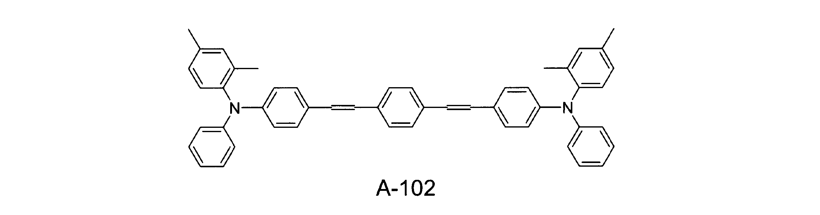
バインダー樹脂、正孔輸送物質および電子輸送物質について、下記の表5中に示すように変更した以外は、実施例23と同様の方法で、電子写真用感光体を作製した。
なお、各実施例において使用した一般式(1)で表される正孔輸送物質の正孔移動度は、その分子構造から、いずれも電界強度を20V/μmとしたとき60×10-6~120×10-6[cm2/V・s]の範囲内にあると推定される。
下記の表中で使用した材料の構造式を、以下に示す。
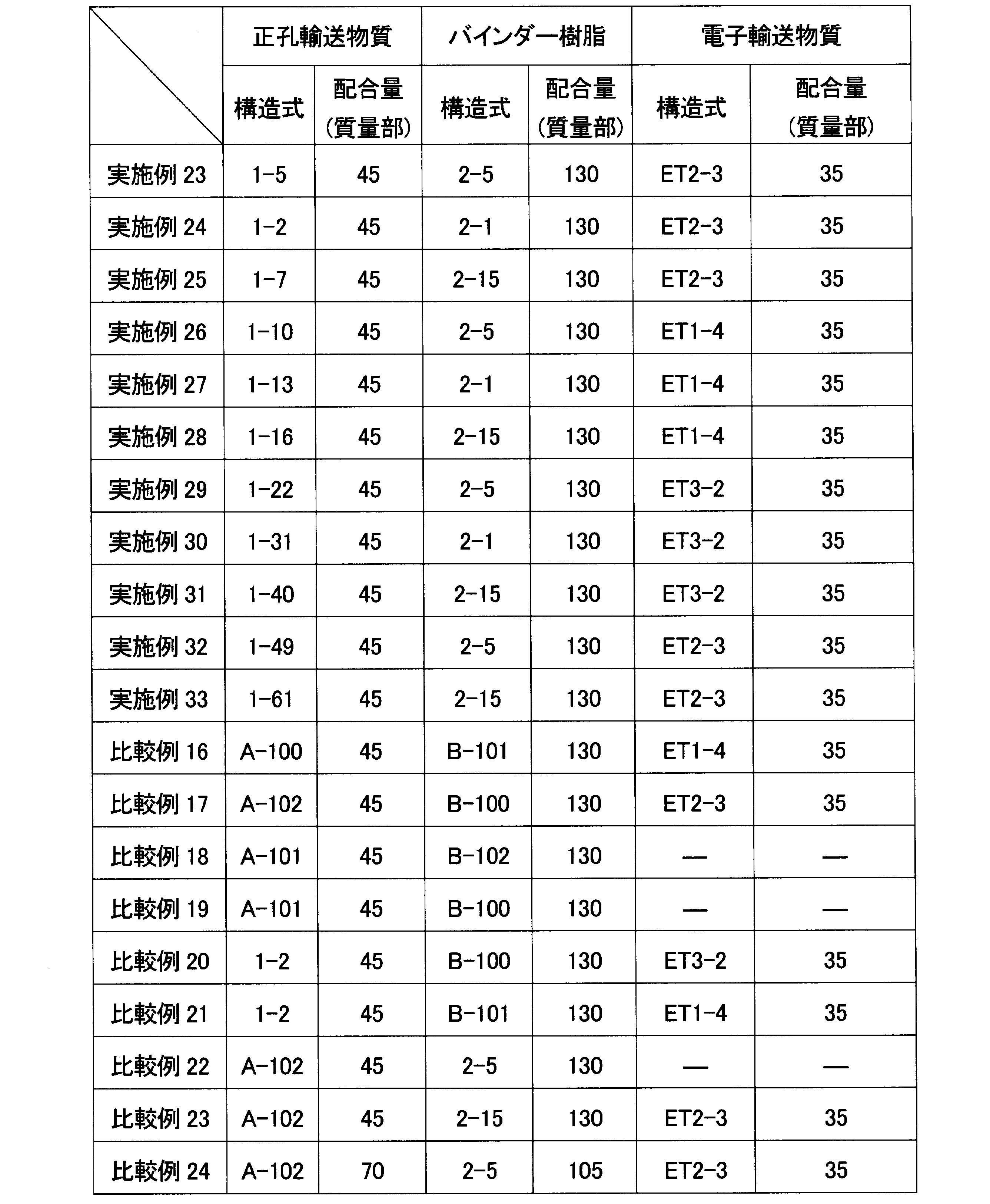
実施例23~33および比較例16~24において作製した電子写真用感光体の電気特性を以下に示す評価方法にて評価した。各実施例および比較例の感光体の電位安定性、耐摩耗性、耐光性、フィルミング、および、耐汚染性について、使用するプリンターをブラザー社製のプリンターHL‐2040に変えた以外は負帯電積層型感光体の例と同様にして、評価を行った。その結果を、下記の表中に示す。
(電気特性の評価)
各実施例および比較例にて得られた感光体の電気特性を、ジェンテック社製のプロセスシミュレーター(CYNTHIA91)を使用して、以下の方法で評価した。実施例23~33および比較例16~24の感光体について、温度22℃、湿度50%の環境下で、感光体の表面を暗所にてコロナ放電により650Vに帯電せしめた後、暗所で5秒間放置した。
次に、ハロゲンランプを光源とし、フィルターを用いて780nmに分光した1.0μW/cm2の露光光を、表面電位が600Vになった時点から感光体に5秒間照射した。表面電位が300Vとなるまで光減衰するのに要する露光量をE1/2(μJ/cm2)とし、露光後5秒後の感光体表面の残留電位をVr5(V)とした。
各実施例および比較例にて得られた感光体の電気特性を、ジェンテック社製のプロセスシミュレーター(CYNTHIA91)を使用して、以下の方法で評価した。実施例23~33および比較例16~24の感光体について、温度22℃、湿度50%の環境下で、感光体の表面を暗所にてコロナ放電により650Vに帯電せしめた後、暗所で5秒間放置した。
次に、ハロゲンランプを光源とし、フィルターを用いて780nmに分光した1.0μW/cm2の露光光を、表面電位が600Vになった時点から感光体に5秒間照射した。表面電位が300Vとなるまで光減衰するのに要する露光量をE1/2(μJ/cm2)とし、露光後5秒後の感光体表面の残留電位をVr5(V)とした。
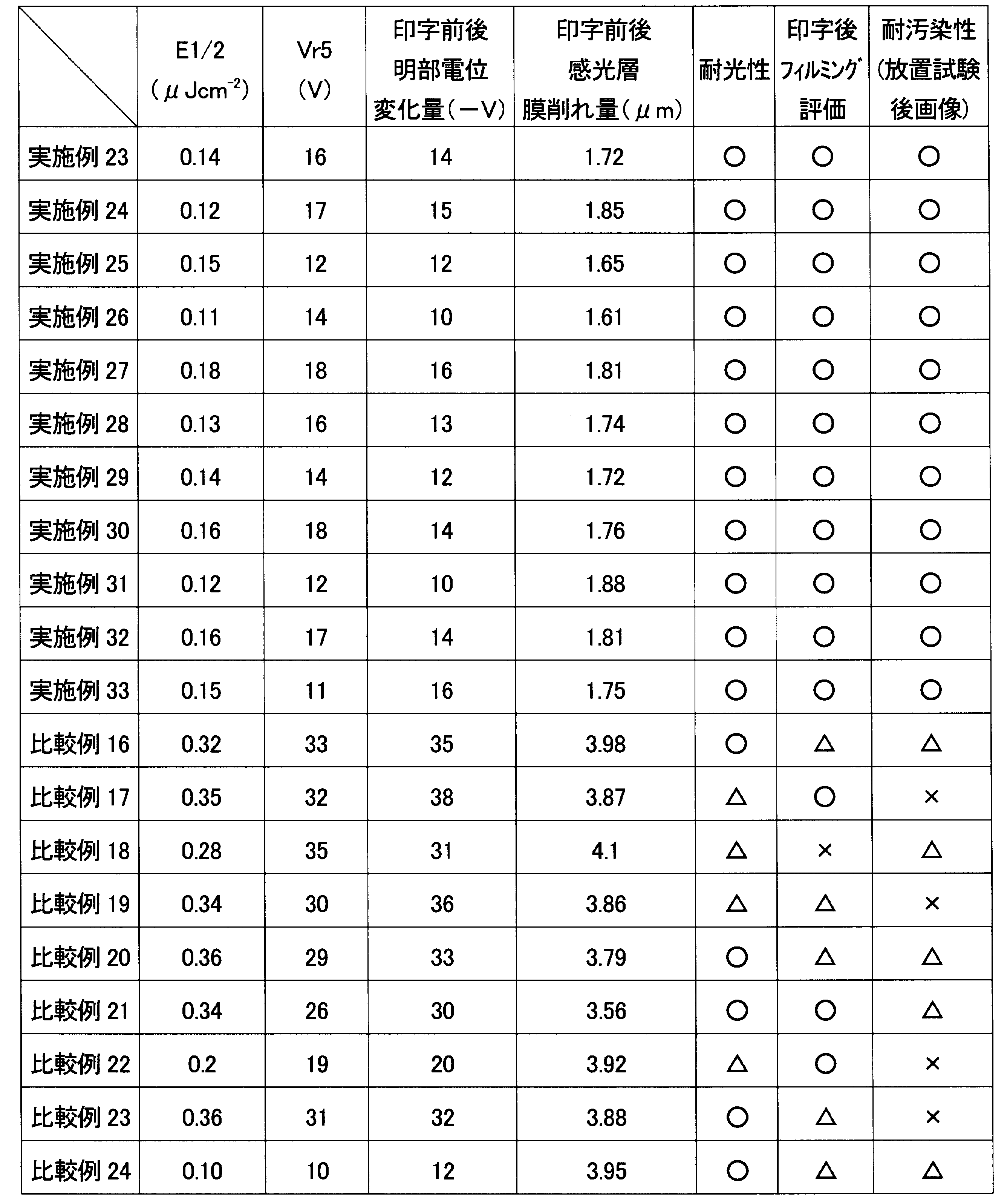
上記表中の結果から、正帯電単層型感光体の感光層中に特定の高移動度正孔輸送物質、ポリカーボネート樹脂および電子輸送物質の組合せを含有させることにより、耐汚染性を改善するとともに、比較例対比で1万枚繰り返し印字後の膜削れ量を50%以上低減できることが明らかとなった。また、このとき、印字後の電位および画像評価において問題が見られることはなかった。
(正帯電積層型感光体の製造)
(実施例34)
正孔輸送物質としての下記式、
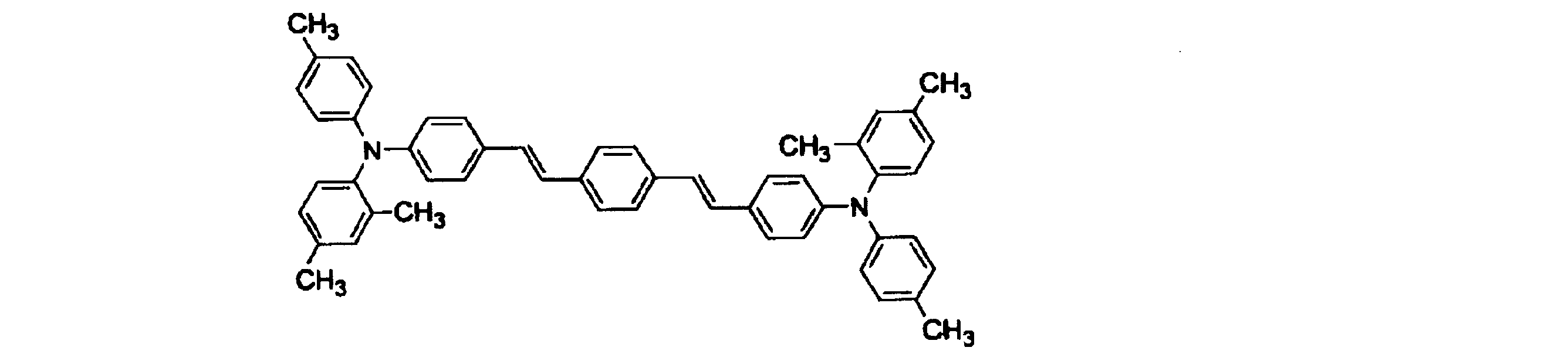 で示される化合物50質量部と、バインダー樹脂としてのビスフェノールZ型ポリカーボネート50質量部とを、ジクロロメタン800質量部に溶解して、電荷輸送層用塗布液を調製した。導電性基体1としての外径24mmのアルミニウム製円筒の外周に、この電荷輸送層用塗布液を浸漬塗工し、温度120℃で60分間乾燥して、膜厚15μmの電荷輸送層を形成した。
(実施例34)
正孔輸送物質としての下記式、
電荷発生物質としての下記式、
 で示される無金属フタロシアニン1.5質量部(バインダー樹脂100質量部に対し約2.5質量部)と、正孔輸送物質としての上記構造式(1-5)で示される化合物10質量部(バインダー樹脂100質量部に対し約17質量部)と、電子輸送物質としての上記構造式(ET2-3)で示される化合物27.5質量部(バインダー樹脂100質量部に対し約45.8質量部)と、バインダー樹脂としての上記構造式(2-5)で示される樹脂60質量部とを、1、2-ジクロロエタン800質量部に溶解、分散させて電荷発生層用塗布液を調製した。構造式(1-5)で示される化合物の正孔移動度は、電界強度を20V/μmとしたとき75.2×10-6[cm2/V・s]であった。バインダー樹脂の含有量は、電荷発生層4の固形分に対し約61質量%であった。
上記電荷輸送層上に、電荷発生層用塗布液を浸漬塗工し、温度100℃で60分間乾燥して、膜厚15μmの電荷発生層を形成し、正帯電積層型感光体を作製した。
上記電荷輸送層上に、電荷発生層用塗布液を浸漬塗工し、温度100℃で60分間乾燥して、膜厚15μmの電荷発生層を形成し、正帯電積層型感光体を作製した。
(実施例35~44、比較例25~33)
バインダー樹脂、正孔輸送物質および電子輸送物質について、下記の表7中に示すように変更した以外は、実施例34と同様の方法で、電子写真用感光体を作製した。
なお、各実施例において使用した一般式(1)で表される正孔輸送物質の正孔移動度は、その分子構造から、いずれも電界強度を20V/μmとしたとき60×10-6~120×10-6[cm2/V・s]の範囲内にあると推定される。
バインダー樹脂、正孔輸送物質および電子輸送物質について、下記の表7中に示すように変更した以外は、実施例34と同様の方法で、電子写真用感光体を作製した。
なお、各実施例において使用した一般式(1)で表される正孔輸送物質の正孔移動度は、その分子構造から、いずれも電界強度を20V/μmとしたとき60×10-6~120×10-6[cm2/V・s]の範囲内にあると推定される。

実施例34~44および比較例25~33において作製した感光体の電気特性、電位安定性、耐摩耗性、耐光性、フィルミング、および、耐汚染性について、正帯電単層型感光体の例と同様にして、評価を行った。その結果を、下記の表中に示す。

上記表中の結果から、正帯電積層型感光体の電荷発生層中に特定の高移動度正孔輸送物質、ポリカーボネート樹脂および電子輸送物質の組合せを含有させることにより、耐汚染性を改善するとともに、比較例対比で1万枚繰り返し印字後の膜削れ量を50%以上低減できることが明らかとなった。また、このとき、印字後の電位および画像評価において問題が見られることはなかった。
1 導電性基体
2 下引き層
3 正帯電単層型の感光層
4 電荷発生層
5 電荷輸送層
6 負帯電積層型の感光層
7 正帯電積層型の感光層
8 感光体
21 ローラ帯電部材
22 高圧電源
23 像露光部材
24 現像器
241 現像ローラ
25 給紙部材
251 給紙ローラ
252 給紙ガイド
26 転写帯電器(直接帯電型)
27 クリーニング装置
271 クリーニングブレード
28 除電部材
60 電子写真装置
300 感光層
2 下引き層
3 正帯電単層型の感光層
4 電荷発生層
5 電荷輸送層
6 負帯電積層型の感光層
7 正帯電積層型の感光層
8 感光体
21 ローラ帯電部材
22 高圧電源
23 像露光部材
24 現像器
241 現像ローラ
25 給紙部材
251 給紙ローラ
252 給紙ガイド
26 転写帯電器(直接帯電型)
27 クリーニング装置
271 クリーニングブレード
28 除電部材
60 電子写真装置
300 感光層
Claims (9)
- 導電性基体と、前記導電性基体上に設けられた感光層と、を含む電子写真用感光体において、
前記感光層が、下記一般式(1)で示される構造を有する正孔輸送物質と、下記一般式(2)で示される繰返し構造を有するバインダー樹脂と、下記一般式(ET1)~(ET3)で示される構造を有する電子輸送物質のうちの少なくとも1種と、を含有する電子写真用感光体。
(式(1)中、R1は水素原子または置換基を有してもよい炭素数1~3のアルキル基を示し、R2~R11は、各々独立に、水素原子、ハロゲン原子、置換基を有してもよい炭素数1~6のアルキル基または置換基を有してもよい炭素数1~6のアルコキシ基を示し、l,m,nは0~4の整数であり、Rは水素原子または置換基を有してもよい炭素数1~3のアルキル基を示す)
(式(2)中、R12~R15は、同一または異なって、水素原子、炭素数1~10のアルキル基または炭素数1~10のフルオロアルキル基を示し、g,h,k,pは0~4の整数であり、s,tは0.3≦t/(s+t)≦0.7を満足し、連鎖末端基は1価の芳香族基または1価のフッ素含有脂肪族基である)
(式(ET1)中、R16,R17は、同一または異なって、水素原子、炭素数1~12のアルキル基、炭素数1~12のアルコキシ基、置換基を有してもよいアリール基、シクロアルキル基、置換基を有してもよいアラルキル基またはハロゲン化アルキル基を表し、R18は、水素原子、炭素数1~6のアルキル基、炭素数1~6のアルコキシ基、置換基を有してもよいアリール基、シクロアルキル基、置換基を有してもよいアラルキル基またはハロゲン化アルキル基を表し、R19~R23は、同一または異なって、水素原子、ハロゲン原子、炭素数1~12のアルキル基、炭素数1~12のアルコキシ基、置換基を有してもよいアリール基、置換基を有してもよいアラルキル基、置換基を有してもよいフェノキシ基、ハロゲン化アルキル基、シアノ基またはニトロ基を表し、また、2つ以上の基が結合して環を形成してもよく、置換基は、ハロゲン原子、炭素数1~6のアルキル基、炭素数1~6のアルコキシ基、水酸基、シアノ基、アミノ基、ニトロ基またはハロゲン化アルキル基を表す)
(式(ET2)中、R24~R29は、同一または異なって、水素原子、ハロゲン原子、シアノ基、ニトロ基、水酸基、炭素数1~12のアルキル基、炭素数1~12のアルコキシ基、置換基を有してもよいアリール基、置換基を有してもよい複素環基、エステル基、シクロアルキル基、置換基を有してもよいアラルキル基、アリル基、アミド基、アミノ基、アシル基、アルケニル基、アルキニル基、カルボキシル基、カルボニル基、カルボン酸基またはハロゲン化アルキル基を表し、置換基は、ハロゲン原子、炭素数1~6のアルキル基、炭素数1~6のアルコキシ基、水酸基、シアノ基、アミノ基、ニトロ基またはハロゲン化アルキル基を表す)
(式(ET3)中、R30,R31は、同一または異なって、水素原子、炭素数1~12のアルキル基、炭素数1~12のアルコキシ基、置換基を有してもよいアリール基、シクロアルキル基、置換基を有してもよいアラルキル基、ハロゲン化アルキル基を表し、置換基は、ハロゲン原子、炭素数1~6のアルキル基、炭素数1~6のアルコキシ基、水酸基、シアノ基、アミノ基、ニトロ基またはハロゲン化アルキル基を表す)
- 前記感光層が、前記導電性基体上に順次積層された電荷発生層と電荷輸送層とを含み、かつ、前記電荷輸送層が、前記正孔輸送物質、前記バインダー樹脂および前記電子輸送物質を含む請求項1記載の電子写真用感光体。
- 前記正孔輸送物質の正孔移動度が60×10-6[cm2/V・s]以上であり、
前記電荷輸送層における前記バインダー樹脂の含有量が、前記電荷輸送層の固形分に対し55質量%以上85質量%以下である請求項2記載の電子写真用感光体。 - 前記感光層が、前記正孔輸送物質、前記バインダー樹脂および前記電子輸送物質を単一層に含む請求項1記載の電子写真用感光体。
- 前記正孔輸送物質の正孔移動度が60×10-6[cm2/V・s]以上であり、
前記感光層における前記バインダー樹脂の含有量が、前記感光層の固形分に対し55質量%以上85質量%以下である請求項1または4記載の電子写真用感光体。 - 前記感光層が、前記導電性基体上に順次積層された電荷輸送層と電荷発生層とを含み、かつ、前記電荷発生層が、前記正孔輸送物質、前記バインダー樹脂および前記電子輸送物質を含む請求項1記載の電子写真用感光体。
- 前記正孔輸送物質の正孔移動度が60×10-6[cm2/V・s]以上であり、
前記電荷発生層における前記バインダー樹脂の含有量が、前記電荷発生層の固形分に対し55質量%以上85質量%以下である請求項6記載の電子写真用感光体。 - 請求項1記載の電子写真用感光体を製造するにあたり、前記導電性基体上に塗布液を塗布して前記感光層を形成する工程を包含する電子写真用感光体の製造方法であって、
前記一般式(1)で示される構造を有する正孔輸送物質と、前記一般式(2)で示される繰返し構造を有するバインダー樹脂と、前記一般式(ET1)~(ET3)で示される構造を有する電子輸送物質のうちの少なくとも1種と、を含有する前記塗布液を準備する工程を備える電子写真用感光体の製造方法。 - 請求項1記載の電子写真用感光体を搭載した電子写真装置。
Priority Applications (4)
| Application Number | Priority Date | Filing Date | Title |
|---|---|---|---|
| PCT/JP2018/005599 WO2019159342A1 (ja) | 2018-02-16 | 2018-02-16 | 電子写真用感光体、その製造方法および電子写真装置 |
| JP2019541822A JP6741165B2 (ja) | 2018-02-16 | 2018-02-16 | 電子写真用感光体、その製造方法および電子写真装置 |
| CN201880009540.2A CN110392865B (zh) | 2018-02-16 | 2018-02-16 | 电子摄影用感光体、其制造方法以及电子摄影装置 |
| US16/523,540 US10747129B2 (en) | 2018-02-16 | 2019-07-26 | Electrophotographic photoconductor, method of manufacturing the same, and electrophotographic apparatus |
Applications Claiming Priority (1)
| Application Number | Priority Date | Filing Date | Title |
|---|---|---|---|
| PCT/JP2018/005599 WO2019159342A1 (ja) | 2018-02-16 | 2018-02-16 | 電子写真用感光体、その製造方法および電子写真装置 |
Related Child Applications (1)
| Application Number | Title | Priority Date | Filing Date |
|---|---|---|---|
| US16/523,540 Continuation US10747129B2 (en) | 2018-02-16 | 2019-07-26 | Electrophotographic photoconductor, method of manufacturing the same, and electrophotographic apparatus |
Publications (1)
| Publication Number | Publication Date |
|---|---|
| WO2019159342A1 true WO2019159342A1 (ja) | 2019-08-22 |
Family
ID=67619228
Family Applications (1)
| Application Number | Title | Priority Date | Filing Date |
|---|---|---|---|
| PCT/JP2018/005599 Ceased WO2019159342A1 (ja) | 2018-02-16 | 2018-02-16 | 電子写真用感光体、その製造方法および電子写真装置 |
Country Status (4)
| Country | Link |
|---|---|
| US (1) | US10747129B2 (ja) |
| JP (1) | JP6741165B2 (ja) |
| CN (1) | CN110392865B (ja) |
| WO (1) | WO2019159342A1 (ja) |
Cited By (6)
| Publication number | Priority date | Publication date | Assignee | Title |
|---|---|---|---|---|
| JP2021139961A (ja) * | 2020-03-02 | 2021-09-16 | 富士電機株式会社 | 電子写真用感光体、その製造方法および電子写真装置 |
| JP2022054800A (ja) * | 2020-09-28 | 2022-04-07 | 京セラドキュメントソリューションズ株式会社 | 電子写真感光体、プロセスカートリッジ、及び画像形成装置 |
| JP2022054802A (ja) * | 2020-09-28 | 2022-04-07 | 京セラドキュメントソリューションズ株式会社 | 電子写真感光体、プロセスカートリッジ、及び画像形成装置 |
| JP2022175953A (ja) * | 2021-05-14 | 2022-11-25 | キヤノン株式会社 | 電子写真装置、プロセスカートリッジ及び画像形成方法 |
| JP2022181417A (ja) * | 2021-05-26 | 2022-12-08 | 京セラドキュメントソリューションズ株式会社 | 電子写真感光体、プロセスカートリッジ、及び画像形成装置 |
| JP2024539817A (ja) * | 2021-08-23 | 2024-10-31 | クロメック グループ ピーエルシー | 材料特性を利用するデバイス性能予測 |
Families Citing this family (4)
| Publication number | Priority date | Publication date | Assignee | Title |
|---|---|---|---|---|
| JP7180176B2 (ja) * | 2018-07-31 | 2022-11-30 | 京セラドキュメントソリューションズ株式会社 | 電子写真感光体 |
| JP7543810B2 (ja) * | 2020-09-28 | 2024-09-03 | 京セラドキュメントソリューションズ株式会社 | 画像形成装置 |
| JP7852506B2 (ja) * | 2020-10-20 | 2026-04-28 | 三菱ケミカル株式会社 | 電子写真感光体、電子写真感光体カートリッジ及び画像形成装置 |
| CN114647161A (zh) * | 2020-12-21 | 2022-06-21 | 富士电机株式会社 | 电子照相用感光体、其制造方法以及电子照相装置 |
Citations (10)
| Publication number | Priority date | Publication date | Assignee | Title |
|---|---|---|---|---|
| JPH03149560A (ja) * | 1989-11-07 | 1991-06-26 | Mitsui Toatsu Chem Inc | 電子写真用感光体 |
| JP2006065083A (ja) * | 2004-08-27 | 2006-03-09 | Kyocera Mita Corp | 湿式現像用電子写真感光体および湿式現像用画像形成装置 |
| JP2006091855A (ja) * | 2004-08-27 | 2006-04-06 | Kyocera Mita Corp | 湿式現像用電子写真感光体及び画像形成装置 |
| JP2007271962A (ja) * | 2006-03-31 | 2007-10-18 | Yamanashi Electronics Co Ltd | 電子写真感光体 |
| JP2014092594A (ja) * | 2012-10-31 | 2014-05-19 | Kyocera Document Solutions Inc | 電子写真感光体及び画像形成装置 |
| WO2014192633A1 (ja) * | 2013-05-27 | 2014-12-04 | 出光興産株式会社 | ポリカーボネート共重合体、それを用いた塗工液、成形体、および電子写真感光体 |
| JP2016142927A (ja) * | 2015-02-02 | 2016-08-08 | 京セラドキュメントソリューションズ株式会社 | 電子写真感光体、電子写真感光体の製造方法、画像形成装置、及びプロセスカートリッジ |
| JP2016224108A (ja) * | 2015-05-27 | 2016-12-28 | 京セラドキュメントソリューションズ株式会社 | 正帯電単層型電子写真感光体、プロセスカートリッジ、及び画像形成装置 |
| JP2017097065A (ja) * | 2015-11-19 | 2017-06-01 | 富士電機株式会社 | 電子写真感光体およびそれを備えた電子写真装置、並びに、電子写真感光体の梱包体 |
| WO2018016156A1 (ja) * | 2016-07-22 | 2018-01-25 | 富士電機株式会社 | 電子写真用感光体、その製造方法および電子写真装置 |
Family Cites Families (18)
| Publication number | Priority date | Publication date | Assignee | Title |
|---|---|---|---|---|
| JPS6162040A (ja) | 1984-09-04 | 1986-03-29 | Fuji Xerox Co Ltd | 電子写真用感光体 |
| JPH01205171A (ja) | 1988-02-10 | 1989-08-17 | Ricoh Co Ltd | 電子写真感光体 |
| JPH04368953A (ja) | 1991-06-18 | 1992-12-21 | Canon Inc | 電子写真感光体、該電子写真感光体を備えた電子写真装置並びにファクシミリ |
| JPH07333881A (ja) | 1994-06-13 | 1995-12-22 | Canon Inc | 電子写真感光体及び該電子写真感光体を備えた電子写真装置 |
| JPH08209023A (ja) | 1994-11-24 | 1996-08-13 | Fuji Electric Co Ltd | チタニルオキシフタロシアニン結晶とその製法及び電子写真感光体 |
| US5874570A (en) | 1995-11-10 | 1999-02-23 | Fuji Electric Co., Ltd. | Titanyloxyphthalocyanine crystals, and method of preparing the same |
| JPH11160958A (ja) | 1997-11-28 | 1999-06-18 | Canon Chemicals Inc | 帯電部材及び電子写真装置 |
| JP3725981B2 (ja) | 1998-07-28 | 2005-12-14 | 三菱化学株式会社 | 電子写真感光体 |
| JP3623662B2 (ja) | 1998-08-24 | 2005-02-23 | 三菱化学株式会社 | 電子写真感光体 |
| JP2002162759A (ja) | 2000-08-28 | 2002-06-07 | Mitsubishi Chemicals Corp | 電子写真感光体 |
| JP2005263737A (ja) | 2004-03-19 | 2005-09-29 | Kyocera Mita Corp | ホルミル化トリフェニルアミン誘導体およびその製造方法 |
| JP2007121733A (ja) | 2005-10-28 | 2007-05-17 | Kyocera Mita Corp | 電子写真感光体 |
| JP2008164757A (ja) | 2006-12-27 | 2008-07-17 | Canon Chemicals Inc | 導電性ゴムローラ及び転写ローラ |
| JP5768556B2 (ja) | 2011-07-22 | 2015-08-26 | 三菱化学株式会社 | 電子写真感光体、電子写真感光体カートリッジ、および画像形成装置 |
| WO2013021430A1 (ja) | 2011-08-05 | 2013-02-14 | 富士電機株式会社 | 電子写真用感光体、その製造方法およびそれを用いた電子写真装置 |
| JP5814212B2 (ja) * | 2012-10-31 | 2015-11-17 | 京セラドキュメントソリューションズ株式会社 | 電子写真感光体及び画像形成装置 |
| JP5787914B2 (ja) * | 2013-01-30 | 2015-09-30 | 京セラドキュメントソリューションズ株式会社 | 正帯電型電子写真感光体及び画像形成装置 |
| WO2015008322A1 (ja) | 2013-07-16 | 2015-01-22 | 富士電機株式会社 | 電子写真用感光体、その製造方法および電子写真装置 |
-
2018
- 2018-02-16 WO PCT/JP2018/005599 patent/WO2019159342A1/ja not_active Ceased
- 2018-02-16 JP JP2019541822A patent/JP6741165B2/ja active Active
- 2018-02-16 CN CN201880009540.2A patent/CN110392865B/zh active Active
-
2019
- 2019-07-26 US US16/523,540 patent/US10747129B2/en active Active
Patent Citations (10)
| Publication number | Priority date | Publication date | Assignee | Title |
|---|---|---|---|---|
| JPH03149560A (ja) * | 1989-11-07 | 1991-06-26 | Mitsui Toatsu Chem Inc | 電子写真用感光体 |
| JP2006065083A (ja) * | 2004-08-27 | 2006-03-09 | Kyocera Mita Corp | 湿式現像用電子写真感光体および湿式現像用画像形成装置 |
| JP2006091855A (ja) * | 2004-08-27 | 2006-04-06 | Kyocera Mita Corp | 湿式現像用電子写真感光体及び画像形成装置 |
| JP2007271962A (ja) * | 2006-03-31 | 2007-10-18 | Yamanashi Electronics Co Ltd | 電子写真感光体 |
| JP2014092594A (ja) * | 2012-10-31 | 2014-05-19 | Kyocera Document Solutions Inc | 電子写真感光体及び画像形成装置 |
| WO2014192633A1 (ja) * | 2013-05-27 | 2014-12-04 | 出光興産株式会社 | ポリカーボネート共重合体、それを用いた塗工液、成形体、および電子写真感光体 |
| JP2016142927A (ja) * | 2015-02-02 | 2016-08-08 | 京セラドキュメントソリューションズ株式会社 | 電子写真感光体、電子写真感光体の製造方法、画像形成装置、及びプロセスカートリッジ |
| JP2016224108A (ja) * | 2015-05-27 | 2016-12-28 | 京セラドキュメントソリューションズ株式会社 | 正帯電単層型電子写真感光体、プロセスカートリッジ、及び画像形成装置 |
| JP2017097065A (ja) * | 2015-11-19 | 2017-06-01 | 富士電機株式会社 | 電子写真感光体およびそれを備えた電子写真装置、並びに、電子写真感光体の梱包体 |
| WO2018016156A1 (ja) * | 2016-07-22 | 2018-01-25 | 富士電機株式会社 | 電子写真用感光体、その製造方法および電子写真装置 |
Cited By (12)
| Publication number | Priority date | Publication date | Assignee | Title |
|---|---|---|---|---|
| JP2021139961A (ja) * | 2020-03-02 | 2021-09-16 | 富士電機株式会社 | 電子写真用感光体、その製造方法および電子写真装置 |
| US11586119B2 (en) | 2020-03-02 | 2023-02-21 | Fuji Electric Co., Ltd. | Electrophotographic photoconductor, method of manufacturing the same, and electrophotographic device |
| JP7443827B2 (ja) | 2020-03-02 | 2024-03-06 | 富士電機株式会社 | 電子写真用感光体、その製造方法および電子写真装置 |
| JP2022054800A (ja) * | 2020-09-28 | 2022-04-07 | 京セラドキュメントソリューションズ株式会社 | 電子写真感光体、プロセスカートリッジ、及び画像形成装置 |
| JP2022054802A (ja) * | 2020-09-28 | 2022-04-07 | 京セラドキュメントソリューションズ株式会社 | 電子写真感光体、プロセスカートリッジ、及び画像形成装置 |
| JP7528679B2 (ja) | 2020-09-28 | 2024-08-06 | 京セラドキュメントソリューションズ株式会社 | 電子写真感光体、プロセスカートリッジ、及び画像形成装置 |
| JP7608763B2 (ja) | 2020-09-28 | 2025-01-07 | 京セラドキュメントソリューションズ株式会社 | 電子写真感光体、プロセスカートリッジ、及び画像形成装置 |
| JP2022175953A (ja) * | 2021-05-14 | 2022-11-25 | キヤノン株式会社 | 電子写真装置、プロセスカートリッジ及び画像形成方法 |
| JP7636959B2 (ja) | 2021-05-14 | 2025-02-27 | キヤノン株式会社 | 電子写真装置、プロセスカートリッジ及び画像形成方法 |
| JP2022181417A (ja) * | 2021-05-26 | 2022-12-08 | 京セラドキュメントソリューションズ株式会社 | 電子写真感光体、プロセスカートリッジ、及び画像形成装置 |
| JP7582071B2 (ja) | 2021-05-26 | 2024-11-13 | 京セラドキュメントソリューションズ株式会社 | 電子写真感光体、プロセスカートリッジ、及び画像形成装置 |
| JP2024539817A (ja) * | 2021-08-23 | 2024-10-31 | クロメック グループ ピーエルシー | 材料特性を利用するデバイス性能予測 |
Also Published As
| Publication number | Publication date |
|---|---|
| CN110392865A (zh) | 2019-10-29 |
| JPWO2019159342A1 (ja) | 2020-02-27 |
| US20190346780A1 (en) | 2019-11-14 |
| CN110392865B (zh) | 2023-08-01 |
| JP6741165B2 (ja) | 2020-08-19 |
| US10747129B2 (en) | 2020-08-18 |
Similar Documents
| Publication | Publication Date | Title |
|---|---|---|
| JP6741165B2 (ja) | 電子写真用感光体、その製造方法および電子写真装置 | |
| JP6432694B2 (ja) | 電子写真用感光体、その製造方法および電子写真装置 | |
| US10254665B2 (en) | Electrophotographic photoreceptor, method for manufacturing the photoreceptor, and electrophotographic apparatus including the photoreceptor | |
| JP6558499B2 (ja) | 電子写真用感光体、その製造方法および電子写真装置 | |
| JP7004011B2 (ja) | 電子写真用感光体、その製造方法および電子写真装置 | |
| CN109643073B (zh) | 电子照相感光体及其制造方法以及使用了电子照相感光体的电子照相装置 | |
| JP6311839B2 (ja) | 電子写真用感光体、その製造方法および電子写真装置 | |
| JP2017097065A (ja) | 電子写真感光体およびそれを備えた電子写真装置、並びに、電子写真感光体の梱包体 | |
| JP2020020908A (ja) | 画像形成装置及び画像形成方法 | |
| WO2019142342A1 (ja) | 電子写真用感光体、その製造方法および電子写真装置 | |
| JP5434246B2 (ja) | 電子写真感光体、並びに該電子写真感光体を用いた電子写真方法、電子写真装置及びプロセスカートリッジ | |
| JP2011257460A (ja) | 正帯電単層型電子写真感光体、及び画像形成装置 | |
| US20040180279A1 (en) | Electrophotographic photoconductor and method of manufacturing the same | |
| JP7187958B2 (ja) | 電子写真用感光体およびそれを搭載した電子写真装置 | |
| JP7346974B2 (ja) | 電子写真用感光体、その製造方法およびそれを搭載した電子写真装置 | |
| US20200363739A1 (en) | Electrophotographic photoreceptor, process for producing the electrophotographic photoreceptor, and electrophotographic device | |
| JP5434255B2 (ja) | 電子写真感光体、並びに該電子写真感光体を用いた電子写真方法、電子写真装置及びプロセスカートリッジ | |
| JP5434260B2 (ja) | 電子写真感光体、並びに該電子写真感光体を用いた電子写真方法、電子写真装置及びプロセスカートリッジ |
Legal Events
| Date | Code | Title | Description |
|---|---|---|---|
| ENP | Entry into the national phase |
Ref document number: 2019541822 Country of ref document: JP Kind code of ref document: A |
|
| 121 | Ep: the epo has been informed by wipo that ep was designated in this application |
Ref document number: 18906293 Country of ref document: EP Kind code of ref document: A1 |
|
| NENP | Non-entry into the national phase |
Ref country code: DE |
|
| 122 | Ep: pct application non-entry in european phase |
Ref document number: 18906293 Country of ref document: EP Kind code of ref document: A1 |