WO2019130474A1 - 半導体装置 - Google Patents
半導体装置 Download PDFInfo
- Publication number
- WO2019130474A1 WO2019130474A1 PCT/JP2017/046929 JP2017046929W WO2019130474A1 WO 2019130474 A1 WO2019130474 A1 WO 2019130474A1 JP 2017046929 W JP2017046929 W JP 2017046929W WO 2019130474 A1 WO2019130474 A1 WO 2019130474A1
- Authority
- WO
- WIPO (PCT)
- Prior art keywords
- heat sink
- semiconductor device
- lead frame
- semiconductor chip
- heat
- Prior art date
- Legal status (The legal status is an assumption and is not a legal conclusion. Google has not performed a legal analysis and makes no representation as to the accuracy of the status listed.)
- Ceased
Links
Images



Classifications
-
- H—ELECTRICITY
- H10—SEMICONDUCTOR DEVICES; ELECTRIC SOLID-STATE DEVICES NOT OTHERWISE PROVIDED FOR
- H10W—GENERIC PACKAGES, INTERCONNECTIONS, CONNECTORS OR OTHER CONSTRUCTIONAL DETAILS OF DEVICES COVERED BY CLASS H10
- H10W40/00—Arrangements for thermal protection or thermal control
- H10W40/20—Arrangements for cooling
- H10W40/22—Arrangements for cooling characterised by their shape, e.g. having conical or cylindrical projections
-
- H—ELECTRICITY
- H10—SEMICONDUCTOR DEVICES; ELECTRIC SOLID-STATE DEVICES NOT OTHERWISE PROVIDED FOR
- H10W—GENERIC PACKAGES, INTERCONNECTIONS, CONNECTORS OR OTHER CONSTRUCTIONAL DETAILS OF DEVICES COVERED BY CLASS H10
- H10W40/00—Arrangements for thermal protection or thermal control
- H10W40/70—Fillings or auxiliary members in containers or in encapsulations for thermal protection or control
- H10W40/77—Auxiliary members characterised by their shape
- H10W40/778—Auxiliary members characterised by their shape in encapsulations
-
- H—ELECTRICITY
- H10—SEMICONDUCTOR DEVICES; ELECTRIC SOLID-STATE DEVICES NOT OTHERWISE PROVIDED FOR
- H10W—GENERIC PACKAGES, INTERCONNECTIONS, CONNECTORS OR OTHER CONSTRUCTIONAL DETAILS OF DEVICES COVERED BY CLASS H10
- H10W40/00—Arrangements for thermal protection or thermal control
- H10W40/60—Securing means for detachable heating or cooling arrangements, e.g. clamps
-
- H—ELECTRICITY
- H10—SEMICONDUCTOR DEVICES; ELECTRIC SOLID-STATE DEVICES NOT OTHERWISE PROVIDED FOR
- H10W—GENERIC PACKAGES, INTERCONNECTIONS, CONNECTORS OR OTHER CONSTRUCTIONAL DETAILS OF DEVICES COVERED BY CLASS H10
- H10W70/00—Package substrates; Interposers; Redistribution layers [RDL]
- H10W70/40—Leadframes
- H10W70/479—Leadframes on or in insulating or insulated package substrates, interposers, or redistribution layers
-
- H—ELECTRICITY
- H10—SEMICONDUCTOR DEVICES; ELECTRIC SOLID-STATE DEVICES NOT OTHERWISE PROVIDED FOR
- H10W—GENERIC PACKAGES, INTERCONNECTIONS, CONNECTORS OR OTHER CONSTRUCTIONAL DETAILS OF DEVICES COVERED BY CLASS H10
- H10W72/00—Interconnections or connectors in packages
-
- H—ELECTRICITY
- H10—SEMICONDUCTOR DEVICES; ELECTRIC SOLID-STATE DEVICES NOT OTHERWISE PROVIDED FOR
- H10W—GENERIC PACKAGES, INTERCONNECTIONS, CONNECTORS OR OTHER CONSTRUCTIONAL DETAILS OF DEVICES COVERED BY CLASS H10
- H10W72/00—Interconnections or connectors in packages
- H10W72/50—Bond wires
-
- H—ELECTRICITY
- H10—SEMICONDUCTOR DEVICES; ELECTRIC SOLID-STATE DEVICES NOT OTHERWISE PROVIDED FOR
- H10W—GENERIC PACKAGES, INTERCONNECTIONS, CONNECTORS OR OTHER CONSTRUCTIONAL DETAILS OF DEVICES COVERED BY CLASS H10
- H10W74/00—Encapsulations, e.g. protective coatings
- H10W74/10—Encapsulations, e.g. protective coatings characterised by their shape or disposition
- H10W74/111—Encapsulations, e.g. protective coatings characterised by their shape or disposition the semiconductor body being completely enclosed
- H10W74/114—Encapsulations, e.g. protective coatings characterised by their shape or disposition the semiconductor body being completely enclosed by a substrate and the encapsulations
-
- H—ELECTRICITY
- H10—SEMICONDUCTOR DEVICES; ELECTRIC SOLID-STATE DEVICES NOT OTHERWISE PROVIDED FOR
- H10W—GENERIC PACKAGES, INTERCONNECTIONS, CONNECTORS OR OTHER CONSTRUCTIONAL DETAILS OF DEVICES COVERED BY CLASS H10
- H10W90/00—Package configurations
- H10W90/701—Package configurations characterised by the relative positions of pads or connectors relative to package parts
-
- H—ELECTRICITY
- H10—SEMICONDUCTOR DEVICES; ELECTRIC SOLID-STATE DEVICES NOT OTHERWISE PROVIDED FOR
- H10W—GENERIC PACKAGES, INTERCONNECTIONS, CONNECTORS OR OTHER CONSTRUCTIONAL DETAILS OF DEVICES COVERED BY CLASS H10
- H10W72/00—Interconnections or connectors in packages
- H10W72/071—Connecting or disconnecting
- H10W72/073—Connecting or disconnecting of die-attach connectors
- H10W72/07331—Connecting techniques
-
- H—ELECTRICITY
- H10—SEMICONDUCTOR DEVICES; ELECTRIC SOLID-STATE DEVICES NOT OTHERWISE PROVIDED FOR
- H10W—GENERIC PACKAGES, INTERCONNECTIONS, CONNECTORS OR OTHER CONSTRUCTIONAL DETAILS OF DEVICES COVERED BY CLASS H10
- H10W72/00—Interconnections or connectors in packages
- H10W72/071—Connecting or disconnecting
- H10W72/073—Connecting or disconnecting of die-attach connectors
- H10W72/07331—Connecting techniques
- H10W72/07336—Soldering or alloying
-
- H—ELECTRICITY
- H10—SEMICONDUCTOR DEVICES; ELECTRIC SOLID-STATE DEVICES NOT OTHERWISE PROVIDED FOR
- H10W—GENERIC PACKAGES, INTERCONNECTIONS, CONNECTORS OR OTHER CONSTRUCTIONAL DETAILS OF DEVICES COVERED BY CLASS H10
- H10W72/00—Interconnections or connectors in packages
- H10W72/30—Die-attach connectors
-
- H—ELECTRICITY
- H10—SEMICONDUCTOR DEVICES; ELECTRIC SOLID-STATE DEVICES NOT OTHERWISE PROVIDED FOR
- H10W—GENERIC PACKAGES, INTERCONNECTIONS, CONNECTORS OR OTHER CONSTRUCTIONAL DETAILS OF DEVICES COVERED BY CLASS H10
- H10W72/00—Interconnections or connectors in packages
- H10W72/30—Die-attach connectors
- H10W72/321—Structures or relative sizes of die-attach connectors
- H10W72/325—Die-attach connectors having a filler embedded in a matrix
-
- H—ELECTRICITY
- H10—SEMICONDUCTOR DEVICES; ELECTRIC SOLID-STATE DEVICES NOT OTHERWISE PROVIDED FOR
- H10W—GENERIC PACKAGES, INTERCONNECTIONS, CONNECTORS OR OTHER CONSTRUCTIONAL DETAILS OF DEVICES COVERED BY CLASS H10
- H10W72/00—Interconnections or connectors in packages
- H10W72/30—Die-attach connectors
- H10W72/351—Materials of die-attach connectors
- H10W72/352—Materials of die-attach connectors comprising metals or metalloids, e.g. solders
-
- H—ELECTRICITY
- H10—SEMICONDUCTOR DEVICES; ELECTRIC SOLID-STATE DEVICES NOT OTHERWISE PROVIDED FOR
- H10W—GENERIC PACKAGES, INTERCONNECTIONS, CONNECTORS OR OTHER CONSTRUCTIONAL DETAILS OF DEVICES COVERED BY CLASS H10
- H10W72/00—Interconnections or connectors in packages
- H10W72/30—Die-attach connectors
- H10W72/351—Materials of die-attach connectors
- H10W72/353—Materials of die-attach connectors not comprising solid metals or solid metalloids, e.g. ceramics
- H10W72/354—Materials of die-attach connectors not comprising solid metals or solid metalloids, e.g. ceramics comprising polymers
-
- H—ELECTRICITY
- H10—SEMICONDUCTOR DEVICES; ELECTRIC SOLID-STATE DEVICES NOT OTHERWISE PROVIDED FOR
- H10W—GENERIC PACKAGES, INTERCONNECTIONS, CONNECTORS OR OTHER CONSTRUCTIONAL DETAILS OF DEVICES COVERED BY CLASS H10
- H10W72/00—Interconnections or connectors in packages
- H10W72/50—Bond wires
- H10W72/541—Dispositions of bond wires
- H10W72/5445—Dispositions of bond wires being orthogonal to a side surface of the chip, e.g. parallel arrangements
-
- H—ELECTRICITY
- H10—SEMICONDUCTOR DEVICES; ELECTRIC SOLID-STATE DEVICES NOT OTHERWISE PROVIDED FOR
- H10W—GENERIC PACKAGES, INTERCONNECTIONS, CONNECTORS OR OTHER CONSTRUCTIONAL DETAILS OF DEVICES COVERED BY CLASS H10
- H10W72/00—Interconnections or connectors in packages
- H10W72/50—Bond wires
- H10W72/541—Dispositions of bond wires
- H10W72/547—Dispositions of multiple bond wires
- H10W72/5475—Dispositions of multiple bond wires multiple bond wires connected to common bond pads at both ends of the wires
-
- H—ELECTRICITY
- H10—SEMICONDUCTOR DEVICES; ELECTRIC SOLID-STATE DEVICES NOT OTHERWISE PROVIDED FOR
- H10W—GENERIC PACKAGES, INTERCONNECTIONS, CONNECTORS OR OTHER CONSTRUCTIONAL DETAILS OF DEVICES COVERED BY CLASS H10
- H10W72/00—Interconnections or connectors in packages
- H10W72/50—Bond wires
- H10W72/551—Materials of bond wires
- H10W72/552—Materials of bond wires comprising metals or metalloids, e.g. silver
-
- H—ELECTRICITY
- H10—SEMICONDUCTOR DEVICES; ELECTRIC SOLID-STATE DEVICES NOT OTHERWISE PROVIDED FOR
- H10W—GENERIC PACKAGES, INTERCONNECTIONS, CONNECTORS OR OTHER CONSTRUCTIONAL DETAILS OF DEVICES COVERED BY CLASS H10
- H10W72/00—Interconnections or connectors in packages
- H10W72/50—Bond wires
- H10W72/551—Materials of bond wires
- H10W72/552—Materials of bond wires comprising metals or metalloids, e.g. silver
- H10W72/5522—Materials of bond wires comprising metals or metalloids, e.g. silver comprising gold [Au]
-
- H—ELECTRICITY
- H10—SEMICONDUCTOR DEVICES; ELECTRIC SOLID-STATE DEVICES NOT OTHERWISE PROVIDED FOR
- H10W—GENERIC PACKAGES, INTERCONNECTIONS, CONNECTORS OR OTHER CONSTRUCTIONAL DETAILS OF DEVICES COVERED BY CLASS H10
- H10W72/00—Interconnections or connectors in packages
- H10W72/50—Bond wires
- H10W72/551—Materials of bond wires
- H10W72/552—Materials of bond wires comprising metals or metalloids, e.g. silver
- H10W72/5524—Materials of bond wires comprising metals or metalloids, e.g. silver comprising aluminium [Al]
-
- H—ELECTRICITY
- H10—SEMICONDUCTOR DEVICES; ELECTRIC SOLID-STATE DEVICES NOT OTHERWISE PROVIDED FOR
- H10W—GENERIC PACKAGES, INTERCONNECTIONS, CONNECTORS OR OTHER CONSTRUCTIONAL DETAILS OF DEVICES COVERED BY CLASS H10
- H10W72/00—Interconnections or connectors in packages
- H10W72/851—Dispositions of multiple connectors or interconnections
- H10W72/874—On different surfaces
- H10W72/884—Die-attach connectors and bond wires
-
- H—ELECTRICITY
- H10—SEMICONDUCTOR DEVICES; ELECTRIC SOLID-STATE DEVICES NOT OTHERWISE PROVIDED FOR
- H10W—GENERIC PACKAGES, INTERCONNECTIONS, CONNECTORS OR OTHER CONSTRUCTIONAL DETAILS OF DEVICES COVERED BY CLASS H10
- H10W74/00—Encapsulations, e.g. protective coatings
-
- H—ELECTRICITY
- H10—SEMICONDUCTOR DEVICES; ELECTRIC SOLID-STATE DEVICES NOT OTHERWISE PROVIDED FOR
- H10W—GENERIC PACKAGES, INTERCONNECTIONS, CONNECTORS OR OTHER CONSTRUCTIONAL DETAILS OF DEVICES COVERED BY CLASS H10
- H10W74/00—Encapsulations, e.g. protective coatings
- H10W74/10—Encapsulations, e.g. protective coatings characterised by their shape or disposition
-
- H—ELECTRICITY
- H10—SEMICONDUCTOR DEVICES; ELECTRIC SOLID-STATE DEVICES NOT OTHERWISE PROVIDED FOR
- H10W—GENERIC PACKAGES, INTERCONNECTIONS, CONNECTORS OR OTHER CONSTRUCTIONAL DETAILS OF DEVICES COVERED BY CLASS H10
- H10W90/00—Package configurations
- H10W90/701—Package configurations characterised by the relative positions of pads or connectors relative to package parts
- H10W90/751—Package configurations characterised by the relative positions of pads or connectors relative to package parts of bond wires
- H10W90/753—Package configurations characterised by the relative positions of pads or connectors relative to package parts of bond wires between laterally-adjacent chips
-
- H—ELECTRICITY
- H10—SEMICONDUCTOR DEVICES; ELECTRIC SOLID-STATE DEVICES NOT OTHERWISE PROVIDED FOR
- H10W—GENERIC PACKAGES, INTERCONNECTIONS, CONNECTORS OR OTHER CONSTRUCTIONAL DETAILS OF DEVICES COVERED BY CLASS H10
- H10W90/00—Package configurations
- H10W90/701—Package configurations characterised by the relative positions of pads or connectors relative to package parts
- H10W90/751—Package configurations characterised by the relative positions of pads or connectors relative to package parts of bond wires
- H10W90/756—Package configurations characterised by the relative positions of pads or connectors relative to package parts of bond wires between a chip and a stacked lead frame, conducting package substrate or heat sink
Definitions
- the present application relates to a semiconductor device, and more particularly to the structure of a semiconductor device provided with a lead frame and a heat sink.
- Mobile phone base stations represent the wireless communications device market.
- Si devices and GaAs devices are currently mainstream.
- semiconductor devices are required to have a wider band and a smaller size due to an increase in communication capacity (see, for example, Patent Document 1). For this reason, while GaN devices are becoming mainstream in fields where high power is being sought, the demand for cost reduction of semiconductor devices is severe.
- a low cost mold package structure in which a lead frame is sealed with a mold resin has been studied.
- a lead frame having a copper or copper alloy-based heat sink is used in order to ensure heat dissipation of the semiconductor chip.
- a semiconductor device in which a dowel provided on the upper surface of a heat sink and a lead frame are fixed by caulking has been developed.
- miniaturization of the package is hindered.
- a structure is known in which trapezoidal protrusions having a long upper side and a short lower side are provided at both ends of a heat dissipation substrate (heat sink) (see, for example, Patent Document 2).
- the lower portion of the lead holder is provided with a groove-shaped recess that matches the above-mentioned trapezoidal convex portion.
- the convex portion and the concave portion are fitted.
- the semiconductor device of this structure is not suitable for realizing the miniaturization of the package.
- JP-A-52-150970 Japanese Patent Application Laid-Open No. 48-066776 JP 2004-103790 A
- the area where the component mounting can not be performed is generated on the upper surface of the heat sink.
- This application is directed to providing a lead frame structure and a semiconductor device capable of component mounting on the entire top surface area of the heat sink.
- a semiconductor device disclosed in the specification of the present application includes a heat sink having a mounting surface, a heat radiation surface, a side surface, and an engagement portion, a semiconductor chip mounted on the mounting surface of the heat sink, and the engagement portion of the heat sink
- the heat sink includes a lead frame engaged with the heat sink, the semiconductor chip, and a molding resin for sealing the lead frame, and the engaging portion of the heat sink is located at a position away from the mounting surface of the heat sink. It is characterized by being arranged.
- a semiconductor device disclosed in the specification of the present application includes a heat sink having a mounting surface, a heat radiation surface, a side surface, and an engagement portion, a semiconductor chip mounted on the mounting surface of the heat sink, and the engagement portion of the heat sink
- the heat sink includes a lead frame engaged with the heat sink, the semiconductor chip, and a molding resin for sealing the lead frame, and the engaging portion of the heat sink is located at a position away from the mounting surface of the heat sink.
- FIG. 2 is a view for explaining the structure of a lead frame in a semiconductor device according to Embodiment 1;
- FIG. 2 is a diagram for explaining the structure of a heat sink in the semiconductor device according to the first embodiment.
- FIG. 2 is a view for explaining the structure of a lead frame in a semiconductor device according to Embodiment 1;
- FIG. 16 is a view for explaining the structure of a lead frame in a semiconductor device according to Embodiment 2;
- FIG. 18 is a view for explaining the structure of a lead frame in a semiconductor device according to Embodiment 3;
- FIG. 18 is a view for explaining the structure of a lead frame in a semiconductor device according to Fourth Embodiment;
- a semiconductor device according to an embodiment of the present invention will be described below with reference to the drawings.
- the same or similar components are denoted by the same reference numerals, and the sizes and scales of the corresponding components are independent of one another.
- the semiconductor device actually includes a plurality of members, in order to simplify the description, only portions necessary for the description are described, and the other portions are omitted.
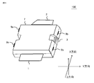
- FIG. 1 is a schematic view showing the appearance of a semiconductor device according to the embodiment.
- the semiconductor device 100 according to the embodiment of the present invention includes the drain electrode terminal 1, the gate electrode terminal 2, the heat sink 3, the mold resin 7, the lead frame 9, and the like.
- a semiconductor chip and a circuit board are mounted on the heat sink 3.
- the semiconductor chip includes a drain electrode, a gate electrode, and a source electrode.
- the semiconductor chip, the circuit board, the lead frame 9 and the heat sink 3 are sealed by the mold resin 7.
- the heat sink 3 has a heat radiation surface (back surface), a mounting surface (upper surface), and a side surface.
- the semiconductor chip and the circuit board are mounted on the mounting surface of the heat sink 3.
- the heat emitted from the semiconductor chip and the circuit board is radiated to the outside from the heat dissipation surface of the heat sink 3.
- the heat sink 3 doubles as a source electrode terminal.
- the semiconductor device 100 according to the embodiment of the present invention is suitable for outputting power with a frequency of 1 GHz or more and 1 W or more.
- the heat sink 3 has a thermal conductivity of 200 mW / K or more.
- Lead frames 9 a and 9 b which are lead-cut are fixed to the back surface (heat radiating surface) of the heat sink 3.
- the semiconductor device (package) is separated into individual pieces by lead cutting the lead frames 9a and 9b.
- the direction from the drain electrode terminal 1 to the gate electrode terminal 2 is referred to as the X direction.
- a direction from the heat dissipating surface (back surface or bottom surface) of the heat sink 3 to the mounting surface (upper surface) of the heat sink 3 will be referred to as a Z direction.
- the direction from the lead frame 9a toward the lead frame 9b is referred to as the Y direction.
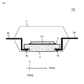
- FIG. 2 is a cross-sectional view showing the structure of the semiconductor device 100 according to the present embodiment.
- the heat sink 3 has a heat radiation surface 3a, a mounting surface 3b and a side surface 3c.
- the semiconductor chip 4 and the circuit board 5 are mounted on the heat sink 3 with a die bonding material 8 such as Ag paste resin, solder, sintered Ag or the like.
- Semiconductor chips 4 such as Si devices, GaAs devices, and GaN devices are disposed on the top surface (mounting surface) of the heat sink 3.
- the drain electrode terminal 1 is connected to the drain electrode of the semiconductor chip 4 by a bonding wire 6.
- the gate electrode terminal 2 is connected to the gate electrode of the semiconductor chip 4 by a bonding wire 6.
- the heat sink 3 is connected to the source electrode of the semiconductor chip 4.
- the semiconductor chip 4 and the circuit board 5 are connected by a bonding wire 6 of Au, Ag, Al or the like, and then sealed by a mold resin 7.
- the back surface (heat dissipation surface) of the heat sink 3 is open and exposed from the mold resin.
- FIG. 3 is a perspective view showing the structure of the heat sink 3 according to the present embodiment.
- the semiconductor chip 4 and the circuit board 5 are fixed to the upper surface (mounting surface) of the heat sink 3 by a die bonding material 8 such as Ag paste resin, solder, sintered Ag or the like.
- the lead frame 9 has leads of two or more terminals. Lead frames 9 a and 9 b are fixed to the back surface (heat dissipating surface) of the heat sink 3.
- the semiconductor chip 4 and the circuit board 5 are wired to the drain electrode terminal 1 and the gate electrode terminal 2 by bonding wires 6.
- the semiconductor chip 4 and the circuit board 5 are sealed with a mold resin 7 in order to protect the semiconductor device 100 from foreign matter, external force, and the like.
- the lead frames 9a and 9b are lead cut. By performing lead cutting on the lead frame 9, the semiconductor device (package) is separated into pieces.
- the direction (X direction) connecting the drain electrode terminal 1 and the gate electrode terminal 2 is orthogonal to the direction (Y direction) connecting the lead frame 9a and the lead frame 9b.
- FIG. 4 is a schematic cross-sectional view showing the structure of the semiconductor device 100 in the present embodiment.
- the semiconductor chip 4 and the circuit board 5 are fixed to the upper surface (mounting surface) of the heat sink 3 by a die bonding material 8 such as Ag paste resin, solder, sintered Ag or the like.
- the lead frame 9 has leads of two or more terminals.
- the heat sink 3 has a dowel 3g on the back surface (heat dissipation surface) side.
- the lead frame 9 and the heat sink 3 are fixed by caulking the dowels 3 g formed on the heat dissipation surface of the heat sink 3 and the lead frames 9 a and 9 b.
- the mold resin 7 seals the semiconductor chip 4 and the circuit board 5 in order to protect the semiconductor device 100 from foreign matter, external force, and the like. By cutting the lead frames 9a and 9b, the semiconductor device (package) is separated into pieces.
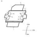
- FIG. 5 is a schematic view showing the structure of the heat sink 3 in the present embodiment.
- the figure shows the shape of the back side of the heat sink 3.
- a dowel 3 g 1 and a dowel 3 g 2, which are engaging portions, are formed on the back surface (heat dissipating surface).
- an engagement hole 9x which is engaged with the dowel 3g is opened.
- the engagement hole 9x of the lead frame 9a is engaged with and engaged with the dowel 3g1.
- the engagement hole 9x of the lead frame 9b is engaged with and engaged with the dowel 3g2.
- the lead frame 9 and the heat sink 3 are fixed by caulking the dowel 3 g of the heat sink 3 and the lead frame 9.
- the semiconductor chip 4 and the circuit board 5 are mounted on the surface (mounting surface) of the heat sink 3.
- the upper surface (mounting surface) of the heat sink does not have a dowel or a caulking. Since the entire top surface of the heat sink can be used for component mounting, the package (semiconductor device) can be miniaturized. That is, since all the upper surfaces (mounting surfaces) of the heat sinks can be used for component mounting in the semiconductor device according to the present embodiment, the package (semiconductor device) can be miniaturized as compared with the conventional case.
- the semiconductor device is a semiconductor device that outputs power with a frequency of 1 GHz or more and 1 W or more, and has a heat sink having a thermal conductivity of 200 mW / K or more and a lead frame having leads of two or more terminals.
- the lead frame and the heat sink are fixed by inserting the lead frame in the groove provided on the side surface of the heat sink, and the Si device, GaAs device, GaN device, Ag paste resin, solder, sintered Ag etc.
- the semiconductor device is a semiconductor device mounted with a die bonding material, wired with a bonding wire of Au, Ag, Al or the like, and sealed with a mold resin.
- a heat sink having a mounting surface, a heat radiation surface, a side surface, and an engaging portion, a semiconductor chip mounted on the mounting surface of the heat sink, and the heat sink
- a lead frame engaged with the joint portion, and the heat sink, the semiconductor chip, and a molded resin sealing the lead frame, wherein the engagement portion of the heat sink avoids the mounting surface of the heat sink It is characterized in that it is placed at
- the semiconductor device 100 includes the drain electrode terminal 1, the gate electrode terminal 2, the heat sink 3, the mold resin 7, the lead frame 9, and the like.
- a semiconductor chip and a circuit board are mounted on the heat sink 3.
- the semiconductor chip includes a drain electrode, a gate electrode, and a source electrode.
- the semiconductor chip, the circuit board, the lead frame 9 and the heat sink 3 are sealed by the mold resin 7.
- the heat sink 3 doubles as a source electrode terminal.
- the semiconductor device 100 is suitable for outputting power with a frequency of 1 GHz or more and 1 W or more.
- the heat sink 3 has a thermal conductivity of 200 mW / K or more.
- the heat sink 3 has a heat radiation surface (back surface), a mounting surface (upper surface), and a side surface.
- the lead frame 9 is fixed to the back surface of the heat sink 3.
- the semiconductor chip and the circuit board are mounted on the mounting surface of the heat sink 3. The heat emitted from the semiconductor chip and the circuit board is radiated to the outside from the heat dissipation surface of the heat sink 3.
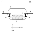
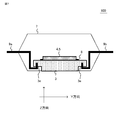
- FIG. 6 is a schematic cross-sectional view showing the structure of the semiconductor device 100 according to the embodiment of the present invention.
- the semiconductor chip 4 and the circuit board 5 are fixed to the upper surface (mounting surface) of the heat sink 3 by a die bonding material 8 such as Ag paste resin, solder, sintered Ag or the like.
- the lead frame 9 has leads of two or more terminals.
- the heat sink 3 has a dowel 3 f which is an engagement portion on the side surface.
- an engagement hole 9x which is engaged with the dowel 3f is opened.
- the engagement hole 9x of the lead frame 9a is engaged with and engaged with the left dowel 3f.
- the engagement hole 9x of the lead frame 9b is engaged with and engaged with the right dowel 3f.
- the lead frame 9 and the heat sink 3 are fixed by caulking the dowels 3 f of the heat sink 3 and the lead frames 9 a and 9 b.
- the mold resin 7 according to the embodiment of the present invention seals the semiconductor chip 4 and the circuit board 5 in order to protect the semiconductor device 100 from foreign matter, external force and the like.
- the semiconductor device 100 according to the present embodiment is a semiconductor device characterized in that the lead frame and the heat sink are fixed by caulking the lead frame on the dowel provided on the side surface of the heat sink.
- the upper surface (mounting surface) of the heat sink does not have a dowel or a caulking. Since all of the top surface (mounting surface) of the heat sink can be used for component mounting, the package (semiconductor device) can be miniaturized. That is, since all the upper surfaces of the heat sink can be used for component mounting in the semiconductor device according to the present embodiment, the package (semiconductor device) can be miniaturized as compared with the related art.
- the semiconductor device 100 includes the drain electrode terminal 1, the gate electrode terminal 2, the heat sink 3, the mold resin 7, the lead frame 9, and the like.
- a semiconductor chip and a circuit board are mounted on the heat sink 3.
- the semiconductor chip includes a drain electrode, a gate electrode, and a source electrode.
- the semiconductor chip, the circuit board, the lead frame 9 and the heat sink 3 are sealed by the mold resin 7.
- the heat sink 3 doubles as a source electrode terminal.
- the semiconductor device 100 is suitable for outputting power with a frequency of 1 GHz or more and 1 W or more.
- the heat sink 3 has a thermal conductivity of 200 mW / K or more.
- the heat sink 3 has a heat radiation surface (back surface), a mounting surface (upper surface), and a side surface.
- the lead frame 9 is fixed to the back surface of the heat sink 3.
- the semiconductor chip and the circuit board are mounted on the mounting surface of the heat sink 3. The heat emitted from the semiconductor chip and the circuit board is radiated to the outside from the heat dissipation surface of the heat sink 3.
- FIG. 7 is a schematic cross-sectional view showing the structure of the semiconductor device 100 according to the embodiment of the present invention.
- the semiconductor chip 4 and the circuit board 5 are fixed to the upper surface (mounting surface) of the heat sink 3 by a die bonding material 8 such as Ag paste resin, solder, sintered Ag or the like.
- the lead frame 9 has leads of two or more terminals.
- the heat sink 3 has a groove 3e which becomes an engaging portion on the back surface. The groove 3 e is formed longitudinally from the back surface to the top surface of the heat sink 3 and does not pierce the top surface of the heat sink.
- a lead frame 9a is engaged with and engaged with the groove 3e on the left side of the heat sink 3.
- the lead frame 9 b is engaged with and engaged with the groove 3 e on the right side of the heat sink 3.
- the lead frame 9 a and the heat sink 3 are fixed by inserting the lead frame 9 a and the lead frame 9 b into the groove 3 e of the heat sink 3.
- the mold resin 7 according to the embodiment of the present invention seals the semiconductor chip 4 and the circuit board 5 in order to protect the semiconductor device 100 from foreign matter, external force and the like.
- the semiconductor device 100 according to the embodiment of the present invention is a semiconductor device characterized in that the lead frame and the heat sink are fixed by inserting the lead frame into the groove provided on the back surface of the heat sink.
- the groove according to the embodiment of the present invention may be V-shaped or U-shaped.
- the package can be miniaturized. That is, since all the upper surfaces of the heat sink can be used for component mounting in the semiconductor device according to the present embodiment, the package (semiconductor device) can be miniaturized as compared with the related art.
- the semiconductor device 100 includes the drain electrode terminal 1, the gate electrode terminal 2, the heat sink 3, the mold resin 7, the lead frame 9, and the like.
- a semiconductor chip and a circuit board are mounted on the heat sink 3.
- the semiconductor chip includes a drain electrode, a gate electrode, and a source electrode.
- the semiconductor chip, the circuit board, the lead frame 9 and the heat sink 3 are sealed by the mold resin 7.
- the heat sink 3 doubles as a source electrode terminal.
- the semiconductor device 100 is suitable for outputting power with a frequency of 1 GHz or more and 1 W or more.
- the heat sink 3 has a thermal conductivity of 200 mW / K or more.
- the heat sink 3 has a heat radiation surface (back surface), a mounting surface (upper surface), and a side surface.
- the lead frame 9 is fixed to the back surface of the heat sink 3.
- the semiconductor chip and the circuit board are mounted on the mounting surface of the heat sink 3. The heat emitted from the semiconductor chip and the circuit board is radiated to the outside from the heat dissipation surface of the heat sink 3.
- FIG. 8 is a schematic cross-sectional view showing the structure of the semiconductor device 100 according to the embodiment of the present invention.
- the semiconductor chip 4 and the circuit board 5 are fixed to the upper surface (mounting surface) of the heat sink 3 by a die bonding material 8 such as Ag paste resin, solder, sintered Ag or the like.
- the lead frame 9 has leads of two or more terminals.
- the heat sink 3 has a groove 3 d as an engaging portion on the side surface. The groove 3 d is formed on the side surface of the heat sink 3 over the entire length of the side surface.
- a lead frame 9a is engaged with and engaged with the groove 3d on the left side of the heat sink 3.
- the lead frame 9 b is engaged with and engaged with the groove 3 d on the right side of the heat sink 3.
- the lead frame 9 a and the heat sink 3 are fixed by inserting the lead frame 9 a and the lead frame 9 b into the groove 3 d of the heat sink 3.
- the mold resin 7 according to the embodiment of the present invention seals the semiconductor chip 4 and the circuit board 5 in order to protect the semiconductor device 100 from foreign matter, external force and the like. Therefore, the semiconductor device according to the embodiment of the present invention is a semiconductor device characterized in that the lead frame and the heat sink are fixed by inserting the lead frame into the groove provided on the side surface of the heat sink.
- the groove according to the embodiment of the present invention may be V-shaped or U-shaped.
- the package can be miniaturized. That is, since the semiconductor device according to the embodiment of the present invention can use the entire top surface of the heat sink for component mounting, the package (semiconductor device) can be miniaturized as compared with the prior art.
Landscapes
- Cooling Or The Like Of Semiconductors Or Solid State Devices (AREA)
- Structures Or Materials For Encapsulating Or Coating Semiconductor Devices Or Solid State Devices (AREA)
- Engineering & Computer Science (AREA)
- Microelectronics & Electronic Packaging (AREA)
- Lead Frames For Integrated Circuits (AREA)
Abstract
Description
本発明の実施の形態に関わる半導体装置の構造を、図を参照しながら説明する。図1は、実施の形態に関わる半導体装置の外観を表している模式図である。本発明の実施の形態に関わる半導体装置100は、ドレイン電極端子1、ゲート電極端子2、ヒートシンク3、モールド樹脂7、リードフレーム9などから構成されている。ヒートシンク3には、半導体チップと回路基板が搭載されている。半導体チップは、ドレイン電極、ゲート電極、ソース電極を備えている。半導体チップ、回路基板、リードフレーム9、およびヒートシンク3は、モールド樹脂7によって、封止されている。
本発明の実施の形態に関わる半導体装置100は、ドレイン電極端子1、ゲート電極端子2、ヒートシンク3、モールド樹脂7、リードフレーム9などから構成されている。ヒートシンク3には、半導体チップと回路基板が搭載されている。半導体チップは、ドレイン電極、ゲート電極、ソース電極を備えている。半導体チップ、回路基板、リードフレーム9、およびヒートシンク3は、モールド樹脂7によって、封止されている。ヒートシンク3は、ソース電極端子を兼ねている。
本発明の実施の形態に関わる半導体装置100は、ドレイン電極端子1、ゲート電極端子2、ヒートシンク3、モールド樹脂7、リードフレーム9などから構成されている。ヒートシンク3には、半導体チップと回路基板が搭載されている。半導体チップは、ドレイン電極、ゲート電極、ソース電極を備えている。半導体チップ、回路基板、リードフレーム9、およびヒートシンク3は、モールド樹脂7によって、封止されている。ヒートシンク3は、ソース電極端子を兼ねている。
本発明の実施の形態に関わる半導体装置100は、ドレイン電極端子1、ゲート電極端子2、ヒートシンク3、モールド樹脂7、リードフレーム9などから構成されている。ヒートシンク3には、半導体チップと回路基板が搭載されている。半導体チップは、ドレイン電極、ゲート電極、ソース電極を備えている。半導体チップ、回路基板、リードフレーム9、およびヒートシンク3は、モールド樹脂7によって、封止されている。ヒートシンク3は、ソース電極端子を兼ねている。
Claims (6)
- 搭載面、放熱面、側面、および係合部を有するヒートシンクと、
前記ヒートシンクの搭載面に搭載されている半導体チップと、
前記ヒートシンクの係合部に係合されているリードフレームと、
前記ヒートシンク、前記半導体チップおよび前記リードフレームを封止しているモールド樹脂と、を備え、
前記ヒートシンクの係合部は、前記ヒートシンクの搭載面を避けた場所に配置されていることを特徴とする半導体装置。 - 前記ヒートシンクの有する係合部は、前記ヒートシンクの有する放熱面に形成されているダボからなることを特徴とする請求項1に記載の半導体装置。
- 前記ヒートシンクの有する係合部は、前記ヒートシンクの有する側面に形成されているダボからなることを特徴とする請求項1に記載の半導体装置。
- 前記ヒートシンクの有する係合部は、前記ヒートシンクの有する放熱面に形成されている溝からなることを特徴とする請求項1に記載の半導体装置。
- 前記ヒートシンクの有する係合部は、前記ヒートシンクの有する側面に形成されている溝からなることを特徴とする請求項1に記載の半導体装置。
- 前記ヒートシンクの有する放熱面は、前記モールド樹脂から露呈していることを特徴とする請求項1から5のいずれか1項に記載の半導体装置。
Priority Applications (6)
| Application Number | Priority Date | Filing Date | Title |
|---|---|---|---|
| DE112017008323.0T DE112017008323T5 (de) | 2017-12-27 | 2017-12-27 | Halbleitervorrichtung |
| PCT/JP2017/046929 WO2019130474A1 (ja) | 2017-12-27 | 2017-12-27 | 半導体装置 |
| US16/756,450 US11335619B2 (en) | 2017-12-27 | 2017-12-27 | Semiconductor device |
| JP2018527244A JP6373545B1 (ja) | 2017-12-27 | 2017-12-27 | 半導体装置 |
| CN201780097906.1A CN111615747B (zh) | 2017-12-27 | 2017-12-27 | 半导体装置 |
| KR1020207016680A KR102351764B1 (ko) | 2017-12-27 | 2017-12-27 | 반도체 장치 |
Applications Claiming Priority (1)
| Application Number | Priority Date | Filing Date | Title |
|---|---|---|---|
| PCT/JP2017/046929 WO2019130474A1 (ja) | 2017-12-27 | 2017-12-27 | 半導体装置 |
Publications (1)
| Publication Number | Publication Date |
|---|---|
| WO2019130474A1 true WO2019130474A1 (ja) | 2019-07-04 |
Family
ID=63165951
Family Applications (1)
| Application Number | Title | Priority Date | Filing Date |
|---|---|---|---|
| PCT/JP2017/046929 Ceased WO2019130474A1 (ja) | 2017-12-27 | 2017-12-27 | 半導体装置 |
Country Status (6)
| Country | Link |
|---|---|
| US (1) | US11335619B2 (ja) |
| JP (1) | JP6373545B1 (ja) |
| KR (1) | KR102351764B1 (ja) |
| CN (1) | CN111615747B (ja) |
| DE (1) | DE112017008323T5 (ja) |
| WO (1) | WO2019130474A1 (ja) |
Cited By (1)
| Publication number | Priority date | Publication date | Assignee | Title |
|---|---|---|---|---|
| WO2023100733A1 (ja) * | 2021-12-01 | 2023-06-08 | ローム株式会社 | 半導体装置、および、半導体装置の製造方法 |
Families Citing this family (2)
| Publication number | Priority date | Publication date | Assignee | Title |
|---|---|---|---|---|
| CN115132673B (zh) * | 2022-06-21 | 2024-09-06 | 维沃移动通信有限公司 | 封装结构及其加工方法、电子设备 |
| CN116705748B (zh) * | 2023-08-08 | 2023-10-17 | 山东隽宇电子科技有限公司 | 一种半导体大面积冷却引线框架 |
Citations (3)
| Publication number | Priority date | Publication date | Assignee | Title |
|---|---|---|---|---|
| JPS60103651A (ja) * | 1983-11-11 | 1985-06-07 | Hitachi Ltd | 半導体装置 |
| JPH10284658A (ja) * | 1997-04-04 | 1998-10-23 | Hitachi Ltd | 半導体装置及びその製造方法 |
| JPH11145364A (ja) * | 1997-11-12 | 1999-05-28 | Denso Corp | 樹脂封止型半導体装置及びその製造方法 |
Family Cites Families (28)
| Publication number | Priority date | Publication date | Assignee | Title |
|---|---|---|---|---|
| JPS514906B2 (ja) | 1971-12-15 | 1976-02-16 | ||
| JPS52105970A (en) | 1976-03-04 | 1977-09-06 | Tdk Electronics Co Ltd | Method of producing magnetic tape storage case |
| JPS52150970A (en) | 1976-06-11 | 1977-12-15 | Hitachi Ltd | Resin molded type semiconductor device |
| JPS58223353A (ja) * | 1982-06-21 | 1983-12-24 | Toshiba Corp | 半導体装置 |
| US5328870A (en) * | 1992-01-17 | 1994-07-12 | Amkor Electronics, Inc. | Method for forming plastic molded package with heat sink for integrated circuit devices |
| JPH0645348U (ja) * | 1992-11-24 | 1994-06-14 | 富士通テン株式会社 | ハイブリッドic用リード端子 |
| KR0137066B1 (ko) * | 1994-09-07 | 1998-04-24 | 황인길 | 히트싱크 내장형 반도체패키지 및 그 제조방법 |
| EP0758488A1 (en) * | 1995-03-06 | 1997-02-19 | National Semiconductor Corporation | Heat sink for integrated circuit packages |
| JPH08255853A (ja) * | 1995-03-16 | 1996-10-01 | Ibiden Co Ltd | 電子部品搭載装置 |
| JP3885321B2 (ja) * | 1997-11-19 | 2007-02-21 | 株式会社デンソー | 樹脂封止型半導体部品の製造方法 |
| KR100259080B1 (ko) * | 1998-02-11 | 2000-06-15 | 김영환 | 히트 스프레드를 갖는 리드 프레임 및 이를 이용한반도체 패키지 |
| JP3854208B2 (ja) | 2002-09-09 | 2006-12-06 | 株式会社三井ハイテック | リードフレームおよびリードフレームの製造方法 |
| JP2004228447A (ja) * | 2003-01-24 | 2004-08-12 | Nec Semiconductors Kyushu Ltd | 半導体装置及びその製造方法 |
| JP2005011899A (ja) * | 2003-06-17 | 2005-01-13 | Himeji Toshiba Ep Corp | リードフレーム及びそれを用いた電子部品 |
| JP4100332B2 (ja) * | 2003-11-12 | 2008-06-11 | 株式会社デンソー | 電子装置およびその製造方法 |
| JP4534675B2 (ja) * | 2004-08-31 | 2010-09-01 | 株式会社デンソー | 集積回路装置 |
| EP1794808B1 (en) | 2004-09-10 | 2017-08-09 | Seoul Semiconductor Co., Ltd. | Light emitting diode package having multiple molding resins |
| JP2006093470A (ja) * | 2004-09-24 | 2006-04-06 | Toshiba Corp | リードフレーム、発光装置、発光装置の製造方法 |
| WO2006080729A1 (en) | 2004-10-07 | 2006-08-03 | Seoul Semiconductor Co., Ltd. | Side illumination lens and luminescent device using the same |
| KR100579397B1 (ko) * | 2004-12-16 | 2006-05-12 | 서울반도체 주식회사 | 리드프레임과 직접 연결된 히트싱크를 채택하는 발광다이오드 패키지 |
| WO2006065007A1 (en) * | 2004-12-16 | 2006-06-22 | Seoul Semiconductor Co., Ltd. | Leadframe having a heat sink supporting ring, fabricating method of a light emitting diodepackage using the same and light emitting diodepackage fabbricated by the method |
| JP4688751B2 (ja) * | 2006-07-25 | 2011-05-25 | 三菱電機株式会社 | 半導体装置 |
| JP2012033665A (ja) * | 2010-07-30 | 2012-02-16 | On Semiconductor Trading Ltd | 半導体装置及びその製造方法 |
| JP2012199436A (ja) * | 2011-03-22 | 2012-10-18 | Toshiba Corp | 半導体装置及びその製造方法 |
| JP5585518B2 (ja) * | 2011-04-08 | 2014-09-10 | 株式会社デンソー | 半導体装置及び半導体装置の製造方法 |
| JP2012248774A (ja) * | 2011-05-31 | 2012-12-13 | Denso Corp | 半導体装置およびその製造方法 |
| JP2015035554A (ja) * | 2013-08-09 | 2015-02-19 | 住友電工デバイス・イノベーション株式会社 | 半導体装置 |
| US10199302B1 (en) * | 2017-08-07 | 2019-02-05 | Nxp Usa, Inc. | Molded air cavity packages and methods for the production thereof |
-
2017
- 2017-12-27 KR KR1020207016680A patent/KR102351764B1/ko active Active
- 2017-12-27 CN CN201780097906.1A patent/CN111615747B/zh active Active
- 2017-12-27 WO PCT/JP2017/046929 patent/WO2019130474A1/ja not_active Ceased
- 2017-12-27 DE DE112017008323.0T patent/DE112017008323T5/de not_active Withdrawn
- 2017-12-27 US US16/756,450 patent/US11335619B2/en active Active
- 2017-12-27 JP JP2018527244A patent/JP6373545B1/ja active Active
Patent Citations (3)
| Publication number | Priority date | Publication date | Assignee | Title |
|---|---|---|---|---|
| JPS60103651A (ja) * | 1983-11-11 | 1985-06-07 | Hitachi Ltd | 半導体装置 |
| JPH10284658A (ja) * | 1997-04-04 | 1998-10-23 | Hitachi Ltd | 半導体装置及びその製造方法 |
| JPH11145364A (ja) * | 1997-11-12 | 1999-05-28 | Denso Corp | 樹脂封止型半導体装置及びその製造方法 |
Cited By (1)
| Publication number | Priority date | Publication date | Assignee | Title |
|---|---|---|---|---|
| WO2023100733A1 (ja) * | 2021-12-01 | 2023-06-08 | ローム株式会社 | 半導体装置、および、半導体装置の製造方法 |
Also Published As
| Publication number | Publication date |
|---|---|
| KR102351764B1 (ko) | 2022-01-14 |
| JPWO2019130474A1 (ja) | 2019-12-26 |
| KR20200087200A (ko) | 2020-07-20 |
| CN111615747B (zh) | 2023-10-03 |
| US20200258806A1 (en) | 2020-08-13 |
| DE112017008323T5 (de) | 2020-09-10 |
| US11335619B2 (en) | 2022-05-17 |
| CN111615747A (zh) | 2020-09-01 |
| JP6373545B1 (ja) | 2018-08-15 |
Similar Documents
| Publication | Publication Date | Title |
|---|---|---|
| JP4698225B2 (ja) | ドレインクリップを備えた半導体ダイパッケージ | |
| CN110071196A (zh) | 具有高效、绝热路径的led封装 | |
| CN104218007B (zh) | 小脚印半导体封装 | |
| KR20100061700A (ko) | 열적으로 강화된 박형 반도체 패키지 | |
| JP2009278103A (ja) | 金属層の間に挟まれたフリップチップダイを特徴とする半導体パッケージ | |
| US9484289B2 (en) | Semiconductor device with heat spreader | |
| US10825753B2 (en) | Semiconductor device and method of manufacture | |
| JP2012199436A (ja) | 半導体装置及びその製造方法 | |
| US10256168B2 (en) | Semiconductor device and lead frame therefor | |
| CN105304506A (zh) | 暴露散热器的方形扁平无引脚(qfn)封装 | |
| JP6373545B1 (ja) | 半導体装置 | |
| CN114899170A (zh) | 一种用于功率氮化镓hemt器件的4引脚to-247封装结构 | |
| US9355946B2 (en) | Converter having partially thinned leadframe with stacked chips and interposer, free of wires and clips | |
| CN112635411A (zh) | 具有顶侧或底侧冷却的半导体封装 | |
| US9743557B2 (en) | Amplifier module with enhanced heat dissipating function and semiconductor device | |
| JP2021082714A (ja) | 半導体装置 | |
| US20180102300A1 (en) | Connectable Package Extender for Semiconductor Device Package | |
| US12159818B2 (en) | Multi-chip packaged semiconductor device | |
| US20110186979A1 (en) | Semiconductor package and high-frequency semiconductor device | |
| KR102305952B1 (ko) | 플립 칩 본딩 기반 반도체 디바이스 패키지 | |
| JP2014003134A (ja) | 高放熱型電子部品収納用パッケージ | |
| JP2006278401A (ja) | 半導体装置 | |
| KR20150142916A (ko) | 반도체 패키지 및 그 제조방법 | |
| CN116895630A (zh) | 电子器件组件和用于制造电子器件组件的方法 | |
| JP2000106415A (ja) | 半導体装置 |
Legal Events
| Date | Code | Title | Description |
|---|---|---|---|
| ENP | Entry into the national phase |
Ref document number: 2018527244 Country of ref document: JP Kind code of ref document: A |
|
| 121 | Ep: the epo has been informed by wipo that ep was designated in this application |
Ref document number: 17936523 Country of ref document: EP Kind code of ref document: A1 |
|
| ENP | Entry into the national phase |
Ref document number: 20207016680 Country of ref document: KR Kind code of ref document: A |
|
| 122 | Ep: pct application non-entry in european phase |
Ref document number: 17936523 Country of ref document: EP Kind code of ref document: A1 |