JP2012199436A - 半導体装置及びその製造方法 - Google Patents
半導体装置及びその製造方法 Download PDFInfo
- Publication number
- JP2012199436A JP2012199436A JP2011063315A JP2011063315A JP2012199436A JP 2012199436 A JP2012199436 A JP 2012199436A JP 2011063315 A JP2011063315 A JP 2011063315A JP 2011063315 A JP2011063315 A JP 2011063315A JP 2012199436 A JP2012199436 A JP 2012199436A
- Authority
- JP
- Japan
- Prior art keywords
- bed
- semiconductor device
- semiconductor element
- pin
- outer peripheral
- Prior art date
- Legal status (The legal status is an assumption and is not a legal conclusion. Google has not performed a legal analysis and makes no representation as to the accuracy of the status listed.)
- Pending
Links
Images


Classifications
-
- H—ELECTRICITY
- H01—ELECTRIC ELEMENTS
- H01L—SEMICONDUCTOR DEVICES NOT COVERED BY CLASS H10
- H01L23/00—Details of semiconductor or other solid state devices
- H01L23/34—Arrangements for cooling, heating, ventilating or temperature compensation ; Temperature sensing arrangements
- H01L23/42—Fillings or auxiliary members in containers or encapsulations selected or arranged to facilitate heating or cooling
- H01L23/433—Auxiliary members in containers characterised by their shape, e.g. pistons
- H01L23/4334—Auxiliary members in encapsulations
-
- H—ELECTRICITY
- H01—ELECTRIC ELEMENTS
- H01L—SEMICONDUCTOR DEVICES NOT COVERED BY CLASS H10
- H01L23/00—Details of semiconductor or other solid state devices
- H01L23/48—Arrangements for conducting electric current to or from the solid state body in operation, e.g. leads, terminal arrangements ; Selection of materials therefor
- H01L23/488—Arrangements for conducting electric current to or from the solid state body in operation, e.g. leads, terminal arrangements ; Selection of materials therefor consisting of soldered or bonded constructions
- H01L23/495—Lead-frames or other flat leads
- H01L23/49541—Geometry of the lead-frame
-
- H—ELECTRICITY
- H01—ELECTRIC ELEMENTS
- H01L—SEMICONDUCTOR DEVICES NOT COVERED BY CLASS H10
- H01L2224/00—Indexing scheme for arrangements for connecting or disconnecting semiconductor or solid-state bodies and methods related thereto as covered by H01L24/00
- H01L2224/01—Means for bonding being attached to, or being formed on, the surface to be connected, e.g. chip-to-package, die-attach, "first-level" interconnects; Manufacturing methods related thereto
- H01L2224/02—Bonding areas; Manufacturing methods related thereto
- H01L2224/04—Structure, shape, material or disposition of the bonding areas prior to the connecting process
- H01L2224/06—Structure, shape, material or disposition of the bonding areas prior to the connecting process of a plurality of bonding areas
- H01L2224/061—Disposition
- H01L2224/0618—Disposition being disposed on at least two different sides of the body, e.g. dual array
- H01L2224/06181—On opposite sides of the body
-
- H—ELECTRICITY
- H01—ELECTRIC ELEMENTS
- H01L—SEMICONDUCTOR DEVICES NOT COVERED BY CLASS H10
- H01L2224/00—Indexing scheme for arrangements for connecting or disconnecting semiconductor or solid-state bodies and methods related thereto as covered by H01L24/00
- H01L2224/01—Means for bonding being attached to, or being formed on, the surface to be connected, e.g. chip-to-package, die-attach, "first-level" interconnects; Manufacturing methods related thereto
- H01L2224/26—Layer connectors, e.g. plate connectors, solder or adhesive layers; Manufacturing methods related thereto
- H01L2224/28—Structure, shape, material or disposition of the layer connectors prior to the connecting process
- H01L2224/29—Structure, shape, material or disposition of the layer connectors prior to the connecting process of an individual layer connector
- H01L2224/29001—Core members of the layer connector
- H01L2224/29099—Material
- H01L2224/291—Material with a principal constituent of the material being a metal or a metalloid, e.g. boron [B], silicon [Si], germanium [Ge], arsenic [As], antimony [Sb], tellurium [Te] and polonium [Po], and alloys thereof
-
- H—ELECTRICITY
- H01—ELECTRIC ELEMENTS
- H01L—SEMICONDUCTOR DEVICES NOT COVERED BY CLASS H10
- H01L2224/00—Indexing scheme for arrangements for connecting or disconnecting semiconductor or solid-state bodies and methods related thereto as covered by H01L24/00
- H01L2224/01—Means for bonding being attached to, or being formed on, the surface to be connected, e.g. chip-to-package, die-attach, "first-level" interconnects; Manufacturing methods related thereto
- H01L2224/26—Layer connectors, e.g. plate connectors, solder or adhesive layers; Manufacturing methods related thereto
- H01L2224/31—Structure, shape, material or disposition of the layer connectors after the connecting process
- H01L2224/32—Structure, shape, material or disposition of the layer connectors after the connecting process of an individual layer connector
- H01L2224/321—Disposition
- H01L2224/32151—Disposition the layer connector connecting between a semiconductor or solid-state body and an item not being a semiconductor or solid-state body, e.g. chip-to-substrate, chip-to-passive
- H01L2224/32221—Disposition the layer connector connecting between a semiconductor or solid-state body and an item not being a semiconductor or solid-state body, e.g. chip-to-substrate, chip-to-passive the body and the item being stacked
- H01L2224/32245—Disposition the layer connector connecting between a semiconductor or solid-state body and an item not being a semiconductor or solid-state body, e.g. chip-to-substrate, chip-to-passive the body and the item being stacked the item being metallic
-
- H—ELECTRICITY
- H01—ELECTRIC ELEMENTS
- H01L—SEMICONDUCTOR DEVICES NOT COVERED BY CLASS H10
- H01L2224/00—Indexing scheme for arrangements for connecting or disconnecting semiconductor or solid-state bodies and methods related thereto as covered by H01L24/00
- H01L2224/01—Means for bonding being attached to, or being formed on, the surface to be connected, e.g. chip-to-package, die-attach, "first-level" interconnects; Manufacturing methods related thereto
- H01L2224/34—Strap connectors, e.g. copper straps for grounding power devices; Manufacturing methods related thereto
- H01L2224/36—Structure, shape, material or disposition of the strap connectors prior to the connecting process
- H01L2224/37—Structure, shape, material or disposition of the strap connectors prior to the connecting process of an individual strap connector
- H01L2224/37001—Core members of the connector
- H01L2224/37099—Material
- H01L2224/371—Material with a principal constituent of the material being a metal or a metalloid, e.g. boron [B], silicon [Si], germanium [Ge], arsenic [As], antimony [Sb], tellurium [Te] and polonium [Po], and alloys thereof
- H01L2224/37117—Material with a principal constituent of the material being a metal or a metalloid, e.g. boron [B], silicon [Si], germanium [Ge], arsenic [As], antimony [Sb], tellurium [Te] and polonium [Po], and alloys thereof the principal constituent melting at a temperature of greater than or equal to 400°C and less than 950°C
- H01L2224/37124—Aluminium [Al] as principal constituent
-
- H—ELECTRICITY
- H01—ELECTRIC ELEMENTS
- H01L—SEMICONDUCTOR DEVICES NOT COVERED BY CLASS H10
- H01L2224/00—Indexing scheme for arrangements for connecting or disconnecting semiconductor or solid-state bodies and methods related thereto as covered by H01L24/00
- H01L2224/01—Means for bonding being attached to, or being formed on, the surface to be connected, e.g. chip-to-package, die-attach, "first-level" interconnects; Manufacturing methods related thereto
- H01L2224/34—Strap connectors, e.g. copper straps for grounding power devices; Manufacturing methods related thereto
- H01L2224/36—Structure, shape, material or disposition of the strap connectors prior to the connecting process
- H01L2224/37—Structure, shape, material or disposition of the strap connectors prior to the connecting process of an individual strap connector
- H01L2224/37001—Core members of the connector
- H01L2224/37099—Material
- H01L2224/371—Material with a principal constituent of the material being a metal or a metalloid, e.g. boron [B], silicon [Si], germanium [Ge], arsenic [As], antimony [Sb], tellurium [Te] and polonium [Po], and alloys thereof
- H01L2224/37138—Material with a principal constituent of the material being a metal or a metalloid, e.g. boron [B], silicon [Si], germanium [Ge], arsenic [As], antimony [Sb], tellurium [Te] and polonium [Po], and alloys thereof the principal constituent melting at a temperature of greater than or equal to 950°C and less than 1550°C
- H01L2224/37147—Copper [Cu] as principal constituent
-
- H—ELECTRICITY
- H01—ELECTRIC ELEMENTS
- H01L—SEMICONDUCTOR DEVICES NOT COVERED BY CLASS H10
- H01L2224/00—Indexing scheme for arrangements for connecting or disconnecting semiconductor or solid-state bodies and methods related thereto as covered by H01L24/00
- H01L2224/01—Means for bonding being attached to, or being formed on, the surface to be connected, e.g. chip-to-package, die-attach, "first-level" interconnects; Manufacturing methods related thereto
- H01L2224/34—Strap connectors, e.g. copper straps for grounding power devices; Manufacturing methods related thereto
- H01L2224/39—Structure, shape, material or disposition of the strap connectors after the connecting process
- H01L2224/40—Structure, shape, material or disposition of the strap connectors after the connecting process of an individual strap connector
- H01L2224/401—Disposition
- H01L2224/40151—Connecting between a semiconductor or solid-state body and an item not being a semiconductor or solid-state body, e.g. chip-to-substrate, chip-to-passive
- H01L2224/40221—Connecting between a semiconductor or solid-state body and an item not being a semiconductor or solid-state body, e.g. chip-to-substrate, chip-to-passive the body and the item being stacked
- H01L2224/40245—Connecting between a semiconductor or solid-state body and an item not being a semiconductor or solid-state body, e.g. chip-to-substrate, chip-to-passive the body and the item being stacked the item being metallic
-
- H—ELECTRICITY
- H01—ELECTRIC ELEMENTS
- H01L—SEMICONDUCTOR DEVICES NOT COVERED BY CLASS H10
- H01L2224/00—Indexing scheme for arrangements for connecting or disconnecting semiconductor or solid-state bodies and methods related thereto as covered by H01L24/00
- H01L2224/01—Means for bonding being attached to, or being formed on, the surface to be connected, e.g. chip-to-package, die-attach, "first-level" interconnects; Manufacturing methods related thereto
- H01L2224/42—Wire connectors; Manufacturing methods related thereto
- H01L2224/44—Structure, shape, material or disposition of the wire connectors prior to the connecting process
- H01L2224/45—Structure, shape, material or disposition of the wire connectors prior to the connecting process of an individual wire connector
- H01L2224/45001—Core members of the connector
- H01L2224/45099—Material
- H01L2224/451—Material with a principal constituent of the material being a metal or a metalloid, e.g. boron (B), silicon (Si), germanium (Ge), arsenic (As), antimony (Sb), tellurium (Te) and polonium (Po), and alloys thereof
- H01L2224/45117—Material with a principal constituent of the material being a metal or a metalloid, e.g. boron (B), silicon (Si), germanium (Ge), arsenic (As), antimony (Sb), tellurium (Te) and polonium (Po), and alloys thereof the principal constituent melting at a temperature of greater than or equal to 400°C and less than 950°C
- H01L2224/45124—Aluminium (Al) as principal constituent
-
- H—ELECTRICITY
- H01—ELECTRIC ELEMENTS
- H01L—SEMICONDUCTOR DEVICES NOT COVERED BY CLASS H10
- H01L2224/00—Indexing scheme for arrangements for connecting or disconnecting semiconductor or solid-state bodies and methods related thereto as covered by H01L24/00
- H01L2224/01—Means for bonding being attached to, or being formed on, the surface to be connected, e.g. chip-to-package, die-attach, "first-level" interconnects; Manufacturing methods related thereto
- H01L2224/42—Wire connectors; Manufacturing methods related thereto
- H01L2224/44—Structure, shape, material or disposition of the wire connectors prior to the connecting process
- H01L2224/45—Structure, shape, material or disposition of the wire connectors prior to the connecting process of an individual wire connector
- H01L2224/45001—Core members of the connector
- H01L2224/45099—Material
- H01L2224/451—Material with a principal constituent of the material being a metal or a metalloid, e.g. boron (B), silicon (Si), germanium (Ge), arsenic (As), antimony (Sb), tellurium (Te) and polonium (Po), and alloys thereof
- H01L2224/45138—Material with a principal constituent of the material being a metal or a metalloid, e.g. boron (B), silicon (Si), germanium (Ge), arsenic (As), antimony (Sb), tellurium (Te) and polonium (Po), and alloys thereof the principal constituent melting at a temperature of greater than or equal to 950°C and less than 1550°C
- H01L2224/45147—Copper (Cu) as principal constituent
-
- H—ELECTRICITY
- H01—ELECTRIC ELEMENTS
- H01L—SEMICONDUCTOR DEVICES NOT COVERED BY CLASS H10
- H01L2224/00—Indexing scheme for arrangements for connecting or disconnecting semiconductor or solid-state bodies and methods related thereto as covered by H01L24/00
- H01L2224/01—Means for bonding being attached to, or being formed on, the surface to be connected, e.g. chip-to-package, die-attach, "first-level" interconnects; Manufacturing methods related thereto
- H01L2224/42—Wire connectors; Manufacturing methods related thereto
- H01L2224/47—Structure, shape, material or disposition of the wire connectors after the connecting process
- H01L2224/48—Structure, shape, material or disposition of the wire connectors after the connecting process of an individual wire connector
- H01L2224/4805—Shape
- H01L2224/4809—Loop shape
- H01L2224/48091—Arched
-
- H—ELECTRICITY
- H01—ELECTRIC ELEMENTS
- H01L—SEMICONDUCTOR DEVICES NOT COVERED BY CLASS H10
- H01L2224/00—Indexing scheme for arrangements for connecting or disconnecting semiconductor or solid-state bodies and methods related thereto as covered by H01L24/00
- H01L2224/01—Means for bonding being attached to, or being formed on, the surface to be connected, e.g. chip-to-package, die-attach, "first-level" interconnects; Manufacturing methods related thereto
- H01L2224/42—Wire connectors; Manufacturing methods related thereto
- H01L2224/47—Structure, shape, material or disposition of the wire connectors after the connecting process
- H01L2224/48—Structure, shape, material or disposition of the wire connectors after the connecting process of an individual wire connector
- H01L2224/481—Disposition
- H01L2224/48151—Connecting between a semiconductor or solid-state body and an item not being a semiconductor or solid-state body, e.g. chip-to-substrate, chip-to-passive
- H01L2224/48221—Connecting between a semiconductor or solid-state body and an item not being a semiconductor or solid-state body, e.g. chip-to-substrate, chip-to-passive the body and the item being stacked
- H01L2224/48245—Connecting between a semiconductor or solid-state body and an item not being a semiconductor or solid-state body, e.g. chip-to-substrate, chip-to-passive the body and the item being stacked the item being metallic
- H01L2224/48247—Connecting between a semiconductor or solid-state body and an item not being a semiconductor or solid-state body, e.g. chip-to-substrate, chip-to-passive the body and the item being stacked the item being metallic connecting the wire to a bond pad of the item
-
- H—ELECTRICITY
- H01—ELECTRIC ELEMENTS
- H01L—SEMICONDUCTOR DEVICES NOT COVERED BY CLASS H10
- H01L2224/00—Indexing scheme for arrangements for connecting or disconnecting semiconductor or solid-state bodies and methods related thereto as covered by H01L24/00
- H01L2224/73—Means for bonding being of different types provided for in two or more of groups H01L2224/10, H01L2224/18, H01L2224/26, H01L2224/34, H01L2224/42, H01L2224/50, H01L2224/63, H01L2224/71
- H01L2224/732—Location after the connecting process
- H01L2224/73201—Location after the connecting process on the same surface
- H01L2224/73221—Strap and wire connectors
-
- H—ELECTRICITY
- H01—ELECTRIC ELEMENTS
- H01L—SEMICONDUCTOR DEVICES NOT COVERED BY CLASS H10
- H01L2224/00—Indexing scheme for arrangements for connecting or disconnecting semiconductor or solid-state bodies and methods related thereto as covered by H01L24/00
- H01L2224/73—Means for bonding being of different types provided for in two or more of groups H01L2224/10, H01L2224/18, H01L2224/26, H01L2224/34, H01L2224/42, H01L2224/50, H01L2224/63, H01L2224/71
- H01L2224/732—Location after the connecting process
- H01L2224/73251—Location after the connecting process on different surfaces
- H01L2224/73263—Layer and strap connectors
-
- H—ELECTRICITY
- H01—ELECTRIC ELEMENTS
- H01L—SEMICONDUCTOR DEVICES NOT COVERED BY CLASS H10
- H01L2224/00—Indexing scheme for arrangements for connecting or disconnecting semiconductor or solid-state bodies and methods related thereto as covered by H01L24/00
- H01L2224/73—Means for bonding being of different types provided for in two or more of groups H01L2224/10, H01L2224/18, H01L2224/26, H01L2224/34, H01L2224/42, H01L2224/50, H01L2224/63, H01L2224/71
- H01L2224/732—Location after the connecting process
- H01L2224/73251—Location after the connecting process on different surfaces
- H01L2224/73265—Layer and wire connectors
-
- H—ELECTRICITY
- H01—ELECTRIC ELEMENTS
- H01L—SEMICONDUCTOR DEVICES NOT COVERED BY CLASS H10
- H01L2224/00—Indexing scheme for arrangements for connecting or disconnecting semiconductor or solid-state bodies and methods related thereto as covered by H01L24/00
- H01L2224/80—Methods for connecting semiconductor or other solid state bodies using means for bonding being attached to, or being formed on, the surface to be connected
- H01L2224/83—Methods for connecting semiconductor or other solid state bodies using means for bonding being attached to, or being formed on, the surface to be connected using a layer connector
- H01L2224/8319—Arrangement of the layer connectors prior to mounting
- H01L2224/83192—Arrangement of the layer connectors prior to mounting wherein the layer connectors are disposed only on another item or body to be connected to the semiconductor or solid-state body
-
- H—ELECTRICITY
- H01—ELECTRIC ELEMENTS
- H01L—SEMICONDUCTOR DEVICES NOT COVERED BY CLASS H10
- H01L2224/00—Indexing scheme for arrangements for connecting or disconnecting semiconductor or solid-state bodies and methods related thereto as covered by H01L24/00
- H01L2224/80—Methods for connecting semiconductor or other solid state bodies using means for bonding being attached to, or being formed on, the surface to be connected
- H01L2224/83—Methods for connecting semiconductor or other solid state bodies using means for bonding being attached to, or being formed on, the surface to be connected using a layer connector
- H01L2224/838—Bonding techniques
- H01L2224/83801—Soldering or alloying
- H01L2224/83815—Reflow soldering
-
- H—ELECTRICITY
- H01—ELECTRIC ELEMENTS
- H01L—SEMICONDUCTOR DEVICES NOT COVERED BY CLASS H10
- H01L2224/00—Indexing scheme for arrangements for connecting or disconnecting semiconductor or solid-state bodies and methods related thereto as covered by H01L24/00
- H01L2224/80—Methods for connecting semiconductor or other solid state bodies using means for bonding being attached to, or being formed on, the surface to be connected
- H01L2224/84—Methods for connecting semiconductor or other solid state bodies using means for bonding being attached to, or being formed on, the surface to be connected using a strap connector
- H01L2224/848—Bonding techniques
- H01L2224/84801—Soldering or alloying
-
- H—ELECTRICITY
- H01—ELECTRIC ELEMENTS
- H01L—SEMICONDUCTOR DEVICES NOT COVERED BY CLASS H10
- H01L2224/00—Indexing scheme for arrangements for connecting or disconnecting semiconductor or solid-state bodies and methods related thereto as covered by H01L24/00
- H01L2224/91—Methods for connecting semiconductor or solid state bodies including different methods provided for in two or more of groups H01L2224/80 - H01L2224/90
- H01L2224/92—Specific sequence of method steps
- H01L2224/922—Connecting different surfaces of the semiconductor or solid-state body with connectors of different types
- H01L2224/9222—Sequential connecting processes
- H01L2224/92242—Sequential connecting processes the first connecting process involving a layer connector
- H01L2224/92246—Sequential connecting processes the first connecting process involving a layer connector the second connecting process involving a strap connector
-
- H—ELECTRICITY
- H01—ELECTRIC ELEMENTS
- H01L—SEMICONDUCTOR DEVICES NOT COVERED BY CLASS H10
- H01L2224/00—Indexing scheme for arrangements for connecting or disconnecting semiconductor or solid-state bodies and methods related thereto as covered by H01L24/00
- H01L2224/91—Methods for connecting semiconductor or solid state bodies including different methods provided for in two or more of groups H01L2224/80 - H01L2224/90
- H01L2224/92—Specific sequence of method steps
- H01L2224/922—Connecting different surfaces of the semiconductor or solid-state body with connectors of different types
- H01L2224/9222—Sequential connecting processes
- H01L2224/92242—Sequential connecting processes the first connecting process involving a layer connector
- H01L2224/92247—Sequential connecting processes the first connecting process involving a layer connector the second connecting process involving a wire connector
-
- H—ELECTRICITY
- H01—ELECTRIC ELEMENTS
- H01L—SEMICONDUCTOR DEVICES NOT COVERED BY CLASS H10
- H01L23/00—Details of semiconductor or other solid state devices
- H01L23/28—Encapsulations, e.g. encapsulating layers, coatings, e.g. for protection
- H01L23/31—Encapsulations, e.g. encapsulating layers, coatings, e.g. for protection characterised by the arrangement or shape
- H01L23/3107—Encapsulations, e.g. encapsulating layers, coatings, e.g. for protection characterised by the arrangement or shape the device being completely enclosed
-
- H—ELECTRICITY
- H01—ELECTRIC ELEMENTS
- H01L—SEMICONDUCTOR DEVICES NOT COVERED BY CLASS H10
- H01L24/00—Arrangements for connecting or disconnecting semiconductor or solid-state bodies; Methods or apparatus related thereto
- H01L24/01—Means for bonding being attached to, or being formed on, the surface to be connected, e.g. chip-to-package, die-attach, "first-level" interconnects; Manufacturing methods related thereto
- H01L24/26—Layer connectors, e.g. plate connectors, solder or adhesive layers; Manufacturing methods related thereto
- H01L24/28—Structure, shape, material or disposition of the layer connectors prior to the connecting process
- H01L24/29—Structure, shape, material or disposition of the layer connectors prior to the connecting process of an individual layer connector
-
- H—ELECTRICITY
- H01—ELECTRIC ELEMENTS
- H01L—SEMICONDUCTOR DEVICES NOT COVERED BY CLASS H10
- H01L24/00—Arrangements for connecting or disconnecting semiconductor or solid-state bodies; Methods or apparatus related thereto
- H01L24/01—Means for bonding being attached to, or being formed on, the surface to be connected, e.g. chip-to-package, die-attach, "first-level" interconnects; Manufacturing methods related thereto
- H01L24/26—Layer connectors, e.g. plate connectors, solder or adhesive layers; Manufacturing methods related thereto
- H01L24/31—Structure, shape, material or disposition of the layer connectors after the connecting process
- H01L24/32—Structure, shape, material or disposition of the layer connectors after the connecting process of an individual layer connector
-
- H—ELECTRICITY
- H01—ELECTRIC ELEMENTS
- H01L—SEMICONDUCTOR DEVICES NOT COVERED BY CLASS H10
- H01L24/00—Arrangements for connecting or disconnecting semiconductor or solid-state bodies; Methods or apparatus related thereto
- H01L24/01—Means for bonding being attached to, or being formed on, the surface to be connected, e.g. chip-to-package, die-attach, "first-level" interconnects; Manufacturing methods related thereto
- H01L24/34—Strap connectors, e.g. copper straps for grounding power devices; Manufacturing methods related thereto
- H01L24/36—Structure, shape, material or disposition of the strap connectors prior to the connecting process
- H01L24/37—Structure, shape, material or disposition of the strap connectors prior to the connecting process of an individual strap connector
-
- H—ELECTRICITY
- H01—ELECTRIC ELEMENTS
- H01L—SEMICONDUCTOR DEVICES NOT COVERED BY CLASS H10
- H01L24/00—Arrangements for connecting or disconnecting semiconductor or solid-state bodies; Methods or apparatus related thereto
- H01L24/01—Means for bonding being attached to, or being formed on, the surface to be connected, e.g. chip-to-package, die-attach, "first-level" interconnects; Manufacturing methods related thereto
- H01L24/34—Strap connectors, e.g. copper straps for grounding power devices; Manufacturing methods related thereto
- H01L24/39—Structure, shape, material or disposition of the strap connectors after the connecting process
- H01L24/40—Structure, shape, material or disposition of the strap connectors after the connecting process of an individual strap connector
-
- H—ELECTRICITY
- H01—ELECTRIC ELEMENTS
- H01L—SEMICONDUCTOR DEVICES NOT COVERED BY CLASS H10
- H01L24/00—Arrangements for connecting or disconnecting semiconductor or solid-state bodies; Methods or apparatus related thereto
- H01L24/01—Means for bonding being attached to, or being formed on, the surface to be connected, e.g. chip-to-package, die-attach, "first-level" interconnects; Manufacturing methods related thereto
- H01L24/42—Wire connectors; Manufacturing methods related thereto
- H01L24/44—Structure, shape, material or disposition of the wire connectors prior to the connecting process
- H01L24/45—Structure, shape, material or disposition of the wire connectors prior to the connecting process of an individual wire connector
-
- H—ELECTRICITY
- H01—ELECTRIC ELEMENTS
- H01L—SEMICONDUCTOR DEVICES NOT COVERED BY CLASS H10
- H01L24/00—Arrangements for connecting or disconnecting semiconductor or solid-state bodies; Methods or apparatus related thereto
- H01L24/01—Means for bonding being attached to, or being formed on, the surface to be connected, e.g. chip-to-package, die-attach, "first-level" interconnects; Manufacturing methods related thereto
- H01L24/42—Wire connectors; Manufacturing methods related thereto
- H01L24/47—Structure, shape, material or disposition of the wire connectors after the connecting process
- H01L24/48—Structure, shape, material or disposition of the wire connectors after the connecting process of an individual wire connector
-
- H—ELECTRICITY
- H01—ELECTRIC ELEMENTS
- H01L—SEMICONDUCTOR DEVICES NOT COVERED BY CLASS H10
- H01L24/00—Arrangements for connecting or disconnecting semiconductor or solid-state bodies; Methods or apparatus related thereto
- H01L24/73—Means for bonding being of different types provided for in two or more of groups H01L24/10, H01L24/18, H01L24/26, H01L24/34, H01L24/42, H01L24/50, H01L24/63, H01L24/71
-
- H—ELECTRICITY
- H01—ELECTRIC ELEMENTS
- H01L—SEMICONDUCTOR DEVICES NOT COVERED BY CLASS H10
- H01L24/00—Arrangements for connecting or disconnecting semiconductor or solid-state bodies; Methods or apparatus related thereto
- H01L24/80—Methods for connecting semiconductor or other solid state bodies using means for bonding being attached to, or being formed on, the surface to be connected
- H01L24/83—Methods for connecting semiconductor or other solid state bodies using means for bonding being attached to, or being formed on, the surface to be connected using a layer connector
-
- H—ELECTRICITY
- H01—ELECTRIC ELEMENTS
- H01L—SEMICONDUCTOR DEVICES NOT COVERED BY CLASS H10
- H01L24/00—Arrangements for connecting or disconnecting semiconductor or solid-state bodies; Methods or apparatus related thereto
- H01L24/80—Methods for connecting semiconductor or other solid state bodies using means for bonding being attached to, or being formed on, the surface to be connected
- H01L24/84—Methods for connecting semiconductor or other solid state bodies using means for bonding being attached to, or being formed on, the surface to be connected using a strap connector
-
- H—ELECTRICITY
- H01—ELECTRIC ELEMENTS
- H01L—SEMICONDUCTOR DEVICES NOT COVERED BY CLASS H10
- H01L24/00—Arrangements for connecting or disconnecting semiconductor or solid-state bodies; Methods or apparatus related thereto
- H01L24/91—Methods for connecting semiconductor or solid state bodies including different methods provided for in two or more of groups H01L24/80 - H01L24/90
- H01L24/92—Specific sequence of method steps
-
- H—ELECTRICITY
- H01—ELECTRIC ELEMENTS
- H01L—SEMICONDUCTOR DEVICES NOT COVERED BY CLASS H10
- H01L2924/00—Indexing scheme for arrangements or methods for connecting or disconnecting semiconductor or solid-state bodies as covered by H01L24/00
- H01L2924/0001—Technical content checked by a classifier
- H01L2924/00011—Not relevant to the scope of the group, the symbol of which is combined with the symbol of this group
-
- H—ELECTRICITY
- H01—ELECTRIC ELEMENTS
- H01L—SEMICONDUCTOR DEVICES NOT COVERED BY CLASS H10
- H01L2924/00—Indexing scheme for arrangements or methods for connecting or disconnecting semiconductor or solid-state bodies as covered by H01L24/00
- H01L2924/0001—Technical content checked by a classifier
- H01L2924/00014—Technical content checked by a classifier the subject-matter covered by the group, the symbol of which is combined with the symbol of this group, being disclosed without further technical details
-
- H—ELECTRICITY
- H01—ELECTRIC ELEMENTS
- H01L—SEMICONDUCTOR DEVICES NOT COVERED BY CLASS H10
- H01L2924/00—Indexing scheme for arrangements or methods for connecting or disconnecting semiconductor or solid-state bodies as covered by H01L24/00
- H01L2924/013—Alloys
- H01L2924/014—Solder alloys
-
- H—ELECTRICITY
- H01—ELECTRIC ELEMENTS
- H01L—SEMICONDUCTOR DEVICES NOT COVERED BY CLASS H10
- H01L2924/00—Indexing scheme for arrangements or methods for connecting or disconnecting semiconductor or solid-state bodies as covered by H01L24/00
- H01L2924/10—Details of semiconductor or other solid state devices to be connected
- H01L2924/11—Device type
- H01L2924/13—Discrete devices, e.g. 3 terminal devices
- H01L2924/1304—Transistor
- H01L2924/1305—Bipolar Junction Transistor [BJT]
- H01L2924/13055—Insulated gate bipolar transistor [IGBT]
-
- H—ELECTRICITY
- H01—ELECTRIC ELEMENTS
- H01L—SEMICONDUCTOR DEVICES NOT COVERED BY CLASS H10
- H01L2924/00—Indexing scheme for arrangements or methods for connecting or disconnecting semiconductor or solid-state bodies as covered by H01L24/00
- H01L2924/10—Details of semiconductor or other solid state devices to be connected
- H01L2924/11—Device type
- H01L2924/13—Discrete devices, e.g. 3 terminal devices
- H01L2924/1304—Transistor
- H01L2924/1306—Field-effect transistor [FET]
- H01L2924/13091—Metal-Oxide-Semiconductor Field-Effect Transistor [MOSFET]
-
- H—ELECTRICITY
- H01—ELECTRIC ELEMENTS
- H01L—SEMICONDUCTOR DEVICES NOT COVERED BY CLASS H10
- H01L2924/00—Indexing scheme for arrangements or methods for connecting or disconnecting semiconductor or solid-state bodies as covered by H01L24/00
- H01L2924/15—Details of package parts other than the semiconductor or other solid state devices to be connected
- H01L2924/181—Encapsulation
-
- H—ELECTRICITY
- H01—ELECTRIC ELEMENTS
- H01L—SEMICONDUCTOR DEVICES NOT COVERED BY CLASS H10
- H01L2924/00—Indexing scheme for arrangements or methods for connecting or disconnecting semiconductor or solid-state bodies as covered by H01L24/00
- H01L2924/19—Details of hybrid assemblies other than the semiconductor or other solid state devices to be connected
- H01L2924/191—Disposition
- H01L2924/19101—Disposition of discrete passive components
- H01L2924/19107—Disposition of discrete passive components off-chip wires
Abstract
【課題】製造コストが低く放熱性が高い半導体装置を提供する。
【解決手段】半導体装置100は、複数の電極を有する半導体素子1と、前記半導体素子が第1の半田2を介して搭載され、前記半導体素子を囲む外周部に位置合わせピン3aを有する導電性のベッド3と、前記ベッドから外側に向かって延伸し、前記半導体素子の前記複数の電極と電気的に接続された複数のリード4と、位置合わせ孔5aを先端に有し、前記リードと同じ導電性材料からなり、前記位置合わせ孔に前記位置合わせピンが挿入されて前記ベッドの前記外周部に係合された吊りピン5と、前記半導体素子、前記ベッド、前記リードの一端、及び前記吊りピンを内包し、その外部に前記リードの他端が突出して延伸するモールド樹脂8と、を備える。前記吊りピンは、第2の半田6により前記ベッドの前記外周部に固定されている。
【選択図】図1
Description
本発明の実施形態は、半導体素子が搭載されたベッドと半導体素子の電極を外部に引き出すリードとを備え、樹脂でパッケージされた半導体装置及びその製造方法に関する。
半導体素子を搭載したベッドと、半導体素子の各電極を外部の回路端子に引き出すためのリードとを、モールド樹脂内に封止した半導体装置として、例えば、SOP(Small Outline Package)やQFP(Quad Flat Package)等がある。これらの半導体装置には、放熱性の向上が求められる。放熱性をよくするために、ベッドの半導体素子を搭載した表面とは反対側の表面をモールド樹脂から露出させることが行われる。過渡的な熱伝導を高めて放熱性をさらに向上させるために、ベッドを厚くすることが望ましい。しかしながら、半導体装置の組み立て工程において、ベッドとリードは、通常これらがフレームから延伸して一体化されたリードフレームを用いて供給される。半導体装置の組み立て完成前に、吊りピンによりフレームに連結されたベッドと、直接フレームに連結されたリードとが、金型を用いてリードフレームから切断される。このときに、リードフレーム及びベッドがあまり厚すぎると、金型の寿命を短くするために、製造工程のコストの増加を招く。そこで、吊りピン及びリードを薄く形成したリードフレームと、リードフレームより厚いベッドを別々に用意し、吊りピンの先端とベッドの外周部をかしめ止めすることで、ベッドとリードが一体化したものが用いられている。しかしながら、このベッドとリードのかしめ止めの加工費も、半導体装置の製造コストに大きく影響している。さらなる加工費の低減が望まれる。
製造コストが低く放熱性が高い半導体装置を提供する。
実施形態の半導体装置は、複数の電極を有する半導体素子と、前記半導体素子が第1の半田を介して搭載され、前記半導体素子を囲む外周部に位置合わせピンを有する導電性のベッドと、前記ベッドから外側に向かって延伸し、前記半導体素子の前記複数の電極と電気的に接続された複数のリードと、位置合わせ孔を先端に有し、前記リードと同じ導電性材料からなり、前記位置合わせ孔に前記位置合わせピンが挿入されて前記ベッドの前記外周部に係合された吊りピンと、前記半導体素子、前記ベッド、前記リードの一端、及び前記吊りピンを内包し、その外部に前記リードの他端が突出して延伸するモールド樹脂と、を備える。前記吊りピンは、第2の半田により前記ベッドの前記外周部に固定されている。
以下、本発明の実施の形態について図を参照しながら説明する。実施の形態中の説明で使用する図は、説明を容易にするための模式的なものであり、図中の各要素の形状、寸法、大小関係などは、実際の実施においては必ずしも図に示されたとおりとは限らず、本発明の効果が得られる範囲内で適宜変更可能である。実施例では、モールド樹脂でパッケージされた半導体装置の一例として、MOSFET(Metal Oxide Semiconductor Field Effect Transistor)やIGBT(Insulated Gate Bipolar Transistor)などの電力用半導体素子のチップを半導体素子として備えたSOP8について説明するが、QFP等の他の樹脂パッケージの半導体装置にも適用可能である。また、半導体素子は、実施例では、MOSFETやIGBTなどの半導体チップを例として説明するが、半導体チップに限らず、これらの半導体チップ、コンデンサ、抵抗などの素子と、配線パターン、及び電極パッドなどが表面に形成された配線基板、又はマルチチップモジュールを、半導体素子として用いることも勿論可能である。また、半導体チップは、MOSFETやIGBT等の個別半導体に限らず、発熱が問題となる半導体素子であれば、IC(Integrated Circuit)チップなどでも本発明の適用が可能である。
(第1の実施の形態)
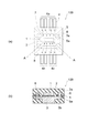
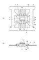
第1の実施の形態について、図1を用いて説明する。図1は、第1の実施形態に係る半導体装置の、(a)平面図、及び(b)(a)のA−A線における断面図である。なお、図1(a)のモールド樹脂8内の平面図は、透視図として描かれている。
第1の実施の形態について、図1を用いて説明する。図1は、第1の実施形態に係る半導体装置の、(a)平面図、及び(b)(a)のA−A線における断面図である。なお、図1(a)のモールド樹脂8内の平面図は、透視図として描かれている。
図1に示したように、本実施形態に係る半導体装置100は、半導体素子1、ベッド3、複数のリード4、吊りピン5、及びモールド樹脂8を備える。半導体素子1は、一例として、MOSFETやIGBT等の電力用半導体素子のチップであり、図示しない複数の電極、例えば、ソース電極、ドレイン電極、及びゲート電極を有する。一例として、ソース電極とゲート電極は、半導体素子1の表面に形成され、ドレイン電極は、半導体素子1の裏面に形成される(図示せず)。半導体素子1は、その裏面が半田2(第1の半田)を介して導電性材料からなるベッド3の表面(第1の主面)に電気的に接続される。すなわち、半導体素子1は、その裏面がベッド3の表面に半田付けされることで、ドレイン電極が、ベッド3に電気的に接続される。ベッド3の材料として、例えば、銅やアルミニウムを用いることができる。
ベッド3は、その外周部3bに表面側(第1の主面側)に突出した位置合わせピン3aを有する。本実施形態の場合は、ベッド3は、矩形の形状を有し、その四隅に位置合わせピン3aを有する。ベッド3は、外周部より半導体素子1が搭載された部分の方が厚く形成される。このため、ベッド3は、表面とは反対側に、外周部より突出した裏面(第2の主面)を有する。以後、ベッド3の厚みは、特に断りがない限り、半導体素子1が搭載されたベッドの部分の厚さを指すこととする。すなわち、ベッド3の厚みは、ベッド3の表面(第1の主面)と裏面(第2の主面)との間隔を示す。
複数のリード4は、ベッドから外側に向かって延伸する。本実施形態の場合は、SOP8を例にあげるため、4本のリードがベッドの一辺から外側に向かって延伸し、これらとは反対側のベッドの他辺から外側に向かって別の4本のリードが延伸する。上記一辺から外側に延伸する4本のリード4aは、例えば、ボンディングワイヤ7を介してベッド3に電気的に接続されて、半導体素子1の裏面に形成された図示しないドレイン電極に第1の半田2を介して電気的に接続される。又は、上記一辺から外側に延伸する4本のリード4aは、ベッド3と一体形成されており、ベッド3の外周部3bの上記一辺から外側に向かって突出して形成されていてもよい(図示せず)。また、上記他辺から外側に延伸する4本のリードのうち、2本のリード4bは、ボンディングワイヤ7により半導体素子1の表面に形成された図示しないソース電極に電気的に接続され、別の2本のリード4cは、ボンディングワイヤ7により半導体素子1の表面に形成された図示しないゲート電極と電気的に接続される。なお、各リードと、ソース電極、ドレイン電極及びゲート電極とのそれぞれの電気的接続は、ボンディングワイヤを一例に示したが、ボンディングワイヤに替えて、アルミニウム又は銅などで構成されるストラップと称する帯状又は短冊状の導電体を用いて行うことも可能である。
吊りピン5は、その先端に位置合わせ孔5aを有し、複数のリードと同じ導電性材料からなる。導電性材料として、アルミニウムや銅などを用いることができる。吊りピン5は、上記ベッド3の外周部3bに形成された位置合わせピン3aが位置合わせ孔5aに挿入されることによって、ベッド3の外周部に係合される。吊りピン5は、その先端に形成された位置合わせ孔5aの形成された部分とベッド3の外周部3bに形成された位置合わせピン3aとを半田6(第2の半田)で接合することで、ベッド3の外周部3bに固定される。吊りピン5は、複数のリード4と同じリードフレームから供給され、両者は同じ材料から構成され、同じ厚さで形成される。ベッド3の厚さは、これらリード4と吊りピン5よりも厚く形成される。ベッド3の材料として、リード4及び吊りピン5同様に、アルミニウム又は銅などを用いることができる。後述の製造方法で説明するとおり、リード4及び吊りピン5は、金型による切断を容易にするために薄く形成することが望ましく、ベッド3は、半導体素子1の放熱性を高めるために厚く形成することが望ましい。
モールド樹脂8は、半導体素子1、ベッド3、リード4及び吊りピン5をその内部に内包するように形成される。半導体素子1は、モールド樹脂8内に完全に埋め込まれる。ベッド3の、半導体素子が搭載された表面(第1の主面)、位置合わせピン3a、及び外周部3は、モールド樹脂により覆われ、外周部3bから突出した第2の主面だけが、モールド樹脂に覆われずに外部に露出する。吊りピン5は、モールド樹脂8内に埋め込まれ、吊りピン5のモールド樹脂8から露出した部分は、切り落とされる。
以上説明したように構成される本実施形態に係る半導体装置100は、以下の特徴を有する。吊りピン5は、上記ベッド3の外周部3bに形成された位置合わせピン3aが位置合わせ孔5aに挿入されることによって、ベッド3の外周部に係合される。吊りピン5は、その先端に形成された位置合わせ孔5aの形成された部分とベッド3の外周部3bに形成された位置合わせピン3aとを半田6(第2の半田)で接合することで、ベッド3の外周部3bに固定される。吊りピン5とベッド3が上記構成を有することにより、後述の製造方法で説明するとおり、本実施形態に係る半導体装置100は、製造コストの増加を抑えながら、リード4及び吊りピン5より厚いベッド3を備えることができる。この結果、動作中に半導体素子1から発生した熱は、半導体素子1の裏面からベッド3へ伝導し、モールド樹脂8から露出したベッド3の裏面より、半導体装置100の外部に効率よく放熱される。ベッド3が厚いほど、過渡的な熱抵抗が低いので、半導体装置100の放熱をさらに向上させることができる。
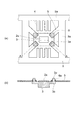
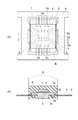
次に、半導体装置100の製造方法について、図2から図5を用いて説明する。図2から図5は、それぞれ、第1の実施形態に係る半導体装置100の製造工程の一部の、(a)平面図、及び(b)(a)のA−A線における断面図である。本実施形態に係る半導体装置100は、以下のように製造される。
まず、図2に示すように、環状(例えば四角形)のフレーム9a内に、複数(本実施形態では一例として8本)のリード4及び複数(本実施形態では一例として4本)の吊りピン5を素子単位に備えたリードフレーム9が用意される。リードフレーム9は、その素子単位を複数有する。8本のリード4のうち4本が、フレーム9aの一辺からフレームの内側に向かって延伸し、残りの4本が上記一辺と対向するフレーム9aの他辺からフレームの内側に向かって延伸する。フレーム9aの一辺から延伸するリード4と、フレーム9aの対向する他辺から延伸するリードとの間には、後述のベッド3が配置されるための空間が設けられる。さらに、吊りピン5が、フレーム9aからベッド3が配置される予定の空間に向かって延伸して形成される。本実施形態では、リード4が延伸するフレーム9aの一辺と直交する別の一辺の両端部から2本の吊りピンが延伸し、この別の一辺と対向する別の他の一辺の両端から2本の吊りピンが延伸する。なお、上記吊りピン5とリード4との配置関係は一例であり、吊りピン5がフレーム9aから延伸してベッド3を支持できる構造であれば、上記構造に限定されることはない。位置合わせ孔5aが、吊りピン5のフレーム9aとは反対側の先端部に設けられる。リードフレーム9は、アルミニウム又は銅により構成され、リード4、吊りピン5、及びフレーム9aは、一様に薄く形成される。
ベッド3が用意される。前述のとおり、ベッド3は、矩形の形状を有し、その外周部3bの四隅に、半導体素子1が搭載される第1の主面側に突出した位置合わせピン3aを有する。ベッド3は、外周部3bより半導体素子1が搭載される部分の方が厚く形成され、半導体素子1が搭載される第1の主面とは反対側に、外周部3bより突出した第2の主面を有する。
上記ベッド3の外周部3bに形成された4本の位置合わせピン3aが、それぞれ、対応する吊りピン5の位置合わせ孔5aに第1の主面側から挿入されることで、リードフレーム9の吊りピン5がベッド3の外周部3bに係合される。この係合により、フレーム9aの一辺から延伸するリード4と、この一辺に対向するフレーム9aの他辺から延伸するリードとの間に、ベッド3が配置されるように、リードフレーム9がベッド3の外周部3bの第1の主面側に仮固定される。このままでは、後述のモールド樹脂でパッケージする工程で、リードフレーム9とベッド3の位置ずれが発生するために、後述するように半田6でリードフレーム9とベッド3が固定される。
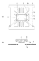
次に、図3に示したように、第1の半田ペースト2aが、ベッド3の第1の主面の半導体素子1が搭載される予定の部分に塗布される。次に、第2の半田ペースト6aが、吊りピン5の先端部の位置合わせ孔5aが形成された部分に塗布されて、ベッド3の位置合わせピン3aと吊りピン5の位置合わせ孔5aが形成された部分とに密着する。
次に、図4に示したように、半導体素子1が第1の半田ペースト2aを介して、ベッド3の第1の主面に搭載される。第1の半田ペースト2aが、半導体素子1の裏面に形成された図示しないドレイン電極とベッド3の第1の主面とに密着する。この後、リフロー工程により、第1の半田ペースト2a及び第2の半田ペースト6aが同時に熔融して固化することで、半導体素子1がベッド3の第1の主面に第1の半田2により接合されると同時に、吊りピン5の位置合わせ孔5aが形成された部分とベッド3の外周部3bの位置合わせピン3aとが、第2の半田6により接合される。すなわち、半導体素子1がベッド3の第1の主面に半田付けにより接合されると同時に、リードフレーム9とベッド3が半田付けにより一体化される。
次に、半導体素子1の複数の電極が、リード4のそれぞれと電気的に接続される。本実施形態の半導体装置100では、フレーム9aの上辺から延伸するリード4aのそれぞれが、ボンディングワイヤ7によりベッド3の第1の主面に電気的に接続されることで、半導体素子1の図示しないドレイン電極に電気的に接続される。フレーム9aの下辺から延伸するリード4bのそれぞれが、ボンディングワイヤ7により半導体素子1の表面に形成された図示しないソース電極に電気的に接続される。フレーム9aの下辺から同様に延伸するリード4cのそれぞれが、ボンディングワイヤ7により半導体素子1の表面に形成された図示しないゲート電極に電気的に接続される。なお、電気的な接続の手段の一例としてボンディングワイヤを例に挙げたが、前述のように、ボンディングワイヤの代わりにアルミニウムや銅などからなる帯状又は短冊状のストラップを用いることもできる。
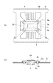
次に、図5に示したように、図示しない金型を用いて、モールド樹脂8が、半導体素子、ベッド、ボンディングワイヤ、吊りピンの一部、及びリードの一端を覆うように形成される。ここで、半導体素子1は、モールド樹脂8内に完全に埋め込まれる。ベッド3の半導体素子1が搭載された表面、位置合わせピン3a、及び外周部3bは、モールド樹脂に覆われ、外周部3bから突出した第2の主面だけが、モールド樹脂に覆われずに外部に露出する。
次に、図示しない金型を用いて、図5中の破線Bの位置で、リード4と吊りピン5が、リードフレーム9のフレーム9aから切断される。複数のリード4の、半導体素子1の各電極とそれぞれ電気的に接続された部分が、モールド樹脂8の内部に埋め込まれ、残りの部分が、モールド樹脂8の外部に延伸する。第2の半田6によりベッド3の外周部3bと固定されている吊りピン5の部分が、モールド樹脂8内に埋め込まれ、吊りピン5の残りの部分が、モールド樹脂8の外部に延伸しないように形成される。
第1の実施形態に係る半導体装置1の上記製造方法では、リフロー工程で半導体素子1がベッド3の第1の主面に半田付けされると同時に、吊りピン5の位置合わせ孔5aが形成された部分が、ベッド3の外周部3bに半田付けされる。これにより、リード4と吊りピン5を有するリードフレーム9と、これらよりも厚いベッド3とが、モールド樹脂8が形成される前に一体化される。この結果、リード4がベッド3から位置ずれすることなく、モールド樹脂8を形成することができる。このベッド3とリードフレーム9との一体化は、リフロー工程で半導体素子1がベッド3の第1の主面に半田付けされると同時に行われるので、新たな工程を必要とせず、リードフレーム9とベッド3に対して特別な加工も必要ない。このため、製造コストの増加が生ずることがない。
これに対して、詳細な説明は省略するが、以下の2つの比較例が代替え技術として考えられる。比較例1は、ベッド3、リード4、及び吊りピン5が一体化したリードフレームを圧延材で厚く形成する方法である。この場合、リード4及び吊りピン5が、リードフレーム9から金型で切断されるときに、金型の切断時のストロークが長くなることで、寿命が短くなるという不利益が生じる。これを避けるため、リード4及び吊りピン5がベッド3より薄くなるように圧延材でリードフレームを形成すると、圧延材の加工費用が増大してしまう。これらは、製造コストの増大を招く。また、比較例2は、リード4及び吊りピン5が一体に形成されたリードフレームと、これらより厚いベッド3とを、本実施形態のように別々に用意し、ベッド3の外周部に吊りピンの先端をかしめ止めすることで両者を一体化する方法である。これも、本実施形態と比較すると、かしめ止めの加工費が発生することで、製造コストの増大をもたらす。
これら比較例と比べて、本実施例に係る半導体装置及びその製造方法は、特別な製造工程の追加及び特別な加工費の発生を生ずることなく、リード4よりも厚いベッド3を用いて半導体装置を製造することができるので、製造費用の増大を抑えながら半導体装置の放熱性を向上することができる。
(第2の実施の形態)
次に第2の実施形態に係る半導体装置200を、図6を用いて説明する。図6は、第2の実施形態に係る半導体装置の、(a)平面図、及び(b)(a)のA−A線における断面図である。なお、図6(a)のモールド樹脂8内の平面図は、透視図として描かれている。なお、第1の実施の形態で説明した構成と同じ構成の部分には同じ参照番号または記号を用いその説明は省略する。第1の実施形態との相異点について主に説明する。
次に第2の実施形態に係る半導体装置200を、図6を用いて説明する。図6は、第2の実施形態に係る半導体装置の、(a)平面図、及び(b)(a)のA−A線における断面図である。なお、図6(a)のモールド樹脂8内の平面図は、透視図として描かれている。なお、第1の実施の形態で説明した構成と同じ構成の部分には同じ参照番号または記号を用いその説明は省略する。第1の実施形態との相異点について主に説明する。
図6に示したように、本実施形態に係る半導体装置200は、ベッド3の外周部3bに形成される位置合わせピン3aが、半導体素子1が搭載される第1の主面と反対側の第2の主面側に突出して形成される点で、第1の実施形態に係る半導体装置100と相異する。この点を除いては、半導体装置200は、第1の実施形態に係る半導体装置100と同じ構造である。
すなわち、ベッド3は、その外周部3bに第1の主面とは反対側の第2の主面側に突出した位置合わせピン3aを有する。第1の実施形態同様に、ベッド3は、矩形の形状を有し、その四隅に位置合わせピン3aを有する。ベッド3は、外周部3bより半導体素子1が搭載される部分の方が厚く形成される。このため、ベッド3は、表面とは反対側に、外周部より突出した第2の主面を有する。
吊りピン5は、その先端部に位置合わせ孔5aを有し、複数のリード4と同じ導電性材料からなる。吊りピン5は、上記ベッド3の外周部3bに形成された位置合わせピン3aが位置合わせ孔5aに挿入されることによって、ベッド3の外周部に係合される。吊りピン5は、その先端に形成された位置合わせ孔5aの形成された部分とベッド3の外周部3bの四隅の1つの側壁とを半田6(第2の半田)で接合することで、ベッド3の外周部3bに固定される。
本実施形態に係る半導体装置200においても、実施形態1に係る半導体装置100と同様に、吊りピン5は、上記ベッド3の外周部3bに形成された位置合わせピン3aが位置合わせ孔5aに挿入されることによって、ベッド3の外周部に係合される。吊りピン5は、その先端部に形成された位置合わせ孔5aの形成された部分とベッド3の外周部3bの四隅の1つの側壁とを半田6(第2の半田)で接合することで、ベッド3の外周部3bに固定される。本実施形態に係る半導体装置200も、第1の実施形態に係る半導体装置100と同様に、製造コストの増加を抑えながら、リード4及び吊りピン5より厚いベッド3を備えることができる。この結果、動作中に半導体素子1から発生した熱は、半導体素子1の裏面からベッド3へ伝導し、モールド樹脂8から露出したベッド3の裏面より、半導体装置100の外部に効率よく放熱される。
次に、本実施形態に係る半導体装置200の製造方法について、図7から図10を用いて説明する。特に断りがない事項に関しては、第1の実施形態に係る半導体装置100の製造方法と同じものとする。図2から図5は、それぞれ、第1の実施形態に係る半導体装置200の製造工程の一部の、(a)平面図、及び(b)(a)のA−A線における断面図である。本実施形態に係る半導体装置100は、以下のように製造される。
まず、図7に示すように、第1の実施形態と同様に、複数のリード4及び吊りピン5を備えたリードフレーム9が用意される。ベッド3が用意される。ベッド3は、矩形の形状を有し、その外周部3bの四隅に、半導体素子1が搭載される第1の主面とは反対側に突出した位置合わせピン3aを有する。ベッド3は、外周部3bより半導体素子1が搭載される部分の方が厚く形成され、半導体素子1が搭載される第1の主面とは反対側に、外周部より突出した第2の主面を有する。
上記ベッド3の外周部3bに形成された4本の位置合わせピン3aが、それぞれ、対応する吊りピン5の位置合わせ孔5aに第2の主面側から挿入されることで、リードフレーム9の吊りピン5がベッド3の外周部3bに係合される。この係合により、フレーム9aの一辺から延伸するリード4と、この一辺に対向するフレーム9aの他辺から延伸するリードとの間に、ベッド3が配置されるように、リードフレーム9がベッド3の外周部3bの第2の主面側に仮固定される。
次に、図8に示したように、第1の半田ペースト2aが、ベッド3の第1の主面の半導体素子1が搭載される予定の部分に塗布される。次に、第2の半田ペースト6aが、吊りピン5の先端部の位置合わせ孔5aが形成された部分に塗布されて、ベッド3の外周部3bの四隅のうちの1つの側壁と吊りピン5の位置合わせ孔5aが形成された部分とに密着する。
次に、図9に示したように、半導体素子1が第1の半田ペースト2aを介して、ベッド3の第1の主面に搭載される。第1の半田ペースト2aが、半導体素子1の裏面に形成された図示しないドレイン電極とベッド3の第1の主面に密着する。この後、リフロー工程により、第1の半田ペースト2a及び第2の半田ペースト6aが同時に熔融して固化することで、半導体素子1がベッド3の第1の主面に第1の半田2により接合されると同時に、吊りピン5の位置合わせ孔5aが形成された部分とベッド3の外周部3bの四隅の側壁とが第2の半田6により接合される。すなわち、半導体素子1がベッド3の第1の主面に半田付けにより接合されると同時に、リードフレーム9とベッド3が半田付けにより一体化される。
次に、第1の実施形態に係る半導体装置100の製造方法と同様に、半導体素子1の複数の電極が、リード4のそれぞれと電気的に接続される。
次に、図10に示したように、第1の実施形態に係る半導体装置100の製造方法と同様に、モールド樹脂8が形成され、リード4と吊りピン5が、リードフレーム9のフレーム9aから切断される。
第1の実施形態同様に、第2の実施形態に係る半導体装置2の上記製造方法では、リフロー工程で半導体素子1がベッド3の第1の主面に半田付けされると同時に、吊りピン5の位置合わせ孔5aが形成された部分がベッド3の外周部3bに半田付けされる。これにより、リード4と吊りピン5を有するリードフレーム9と、これらよりも厚いベッド3とが、モールド樹脂8が形成される前に一体化される。この結果、リード4がベッド3から位置ずれすることなく、モールド樹脂8を形成することができる。このベッド3とリードフレーム9との一体化は、リフロー工程で半導体素子1がベッド3の第1の主面に半田付けされると同時に行われるので、新たな工程を必要とせず、リードフレーム9とベッド3に対して特別な加工も必要ない。このため、製造コストの増加が生ずることがない。本実施形態に係る半導体装置200の製造方法においても、製造費用の増大を抑えながら半導体装置の放熱性を向上することができる。
本発明のいくつかの実施形態を説明したが、これらの実施形態は、例として提示したものであり、発明の範囲を限定することは意図していない。これら新規な実施形態は、その他の様々な形態で実施されることが可能であり、発明の要旨を逸脱しない範囲で、種々の省略、置き換え、変更を行うことができる。これら実施形態やその変形は、発明の範囲や要旨に含まれるとともに、特許請求の範囲に記載された発明とその均等の範囲に含まれる。
1 半導体素子
2 第1の半田
2a 第1の半田ペースト
3 ベッド
3a 位置合わせピン
4 リード
5 吊りピン
5a 位置合わせ孔
6 第2の半田、6a 第2の半田ペースト
7 ボンディングワイヤ
8 モールド樹脂
9 リードフレーム
100、200 半導体装置
2 第1の半田
2a 第1の半田ペースト
3 ベッド
3a 位置合わせピン
4 リード
5 吊りピン
5a 位置合わせ孔
6 第2の半田、6a 第2の半田ペースト
7 ボンディングワイヤ
8 モールド樹脂
9 リードフレーム
100、200 半導体装置
Claims (20)
- 複数の電極を有する半導体素子と、
前記半導体素子が第1の半田を介して搭載され、前記半導体素子を囲む外周部に位置合わせピンを有する導電性のベッドと、
前記ベッドから外側に向かって延伸し、前記半導体素子の前記複数の電極と電気的に接続された複数のリードと、
位置合わせ孔を先端に有し、前記リードと同じ導電性材料からなり、前記位置合わせ孔に前記位置合わせピンが挿入されて前記ベッドの前記外周部に係合された吊りピンと、
前記半導体素子、前記ベッド、前記リードの一端、及び前記吊りピンを内包し、その外部に前記リードの他端が突出して延伸するモールド樹脂と、
を備え、
前記吊りピンは、第2の半田により前記ベッドの前記外周部に固定されていることを特徴とする半導体装置。 - 前記吊りピンの厚さと前記リードの厚さとは、同じであることを特徴とする請求項1記載の半導体装置。
- 前記ベッドは、前記リードより厚いことを特徴とする請求項1又は2に記載の半導体装置。
- 前記ベッドの前記位置合わせピンを有する前記外周部は、前記ベッドの前記半導体素子を搭載する部分より薄いことを特徴とする請求項1〜3のいずれか1つに記載の半導体装置。
- 前記ベッドは、前記半導体素子が搭載された第1の主面と、前記第1の主面と反対側に前記外周部より突出した第2の主面と、を有することを特徴とする請求項1〜4のいずれか1つに記載の半導体装置。
- 前記第1の主面側に前記位置合わせピンが突出していることを特徴とする請求項5記載の半導体装置。
- 前記吊りピンの前記位置合わせ孔が形成された部分は、前記ベッドの外周部の前記位置合わせピンと前記第2の半田により固定されていることを特徴とする請求項6記載の半導体装置。
- 前記第2の主面側に前記位置合わせピンが突出していることを特徴とする請求項5記載の半導体装置。
- 前記吊りピンの前記位置合わせ孔が形成された部分は、前記ベッドの外周部の側壁と前記第2の半田により固定されていることを特徴とする請求項8記載の半導体装置。
- 前記ベッドの第2の主面は、モールド樹脂から露出していることを特徴とする請求項請求項5〜9のいずれか1つに記載の半導体装置。
- 前記半導体素子は、電極、配線層、及び半導体チップが表面に形成された配線基板を含むことを特徴とする請求項1〜10のいずれか1つに記載の半導体装置。
- 環状のフレームから内側に向かって延伸するリード及び吊りピンを有するリードフレームの前記吊りピンの先端に設けられた位置合わせ孔に、導電性のベッドの外周部に設けられた位置合わせピンを挿入することにより、前記リードフレームの前記吊りピンを前記ベッドの前記外周部に係合する工程と、
前記ベッドの中央部に第1の半田ペーストを塗布する工程と、
前記吊りピンの前記先端と前記ベッドの前記外周部とを接続するように第2の半田ペーストを前記吊りピンの前記先端に塗布する工程と、
前記第1の半田ペーストを介して前記ベッドの上に複数の電極を有する半導体素子を搭載する工程と、
前記第1の半田ペーストと前記第2の半田ペーストとを同時にリフローすることにより、前記ベッドへ前記半導体素子を半田付けにより固定すると同時に、前記ベッドの前記外周部へ前記吊りピンの前記先端を半田付けにより固定する工程と、
前記リードを前記半導体素子の複数の電極に電気的に接続させる工程と、
モールド樹脂により、前記半導体素子、前記ベッド、前記吊りピンの一部、及び前記リードの一端を覆う工程と、
前記リードフレームの環状のフレームから、前記リード及び前記吊りピンを切断し、前記リードを前記モールドの外部に延伸するように残す工程と、
を備えたことを特徴とする半導体装置の製造方法。 - 前記吊りピンの厚さと前記リードの厚さと、は同じであり、
前記ベッドは、前記リードより厚いことを特徴とする請求項12記載の半導体装置の製造方法。 - 前記ベッドの前記位置合わせピンを有する前記外周部は、前記ベッドの前記半導体素子を搭載する部分より薄いことを特徴とする請求項12又は13に記載の半導体装置の製造方法。
- 前記ベッドは、前記半導体素子が搭載された第1の主面と、前記第1の主面とは反対側に前記外周部より突出した第2の主面と、を有することを特徴とする請求項12〜14のいずれか1つに記載の半導体装置の製造方法。
- 前記第1の主面側に前記位置合わせピンが突出しており、前記リードフレームの前記吊りピンを前記ベッドの前記外周部に係合する工程において、前記第1の主面側から前記吊りピンの前記位置合わせ孔に前記ベッドの前記位置合わせピンを挿入させることを特徴とする請求項15記載の半導体装置の製造方法。
- 前記第2の半田ペーストを塗布する工程において、前記ベッドの前記外周部の前記位置合わせピンと前記吊りピンの前記位置合わせ孔の部分とを接合するように、前記第2の半田ペーストが塗布されることを特徴とする請求項16記載の半導体装置の製造方法。
- 前記第2の主面側に前記位置合わせピンが突出しており、前記リードフレームの前記吊りピンを前記ベッドの前記外周部に係合する工程において、前記第2の主面側から前記吊りピンの前記位置合わせ孔に前記ベッドの前記位置合わせピンを挿入させることを特徴とする請求項15記載の半導体装置の製造方法。
- 前記第2の半田ペーストを塗布する工程において、前記ベッドの前記外周部の側壁と前記吊りピンの前記位置合わせ孔の部分とを接合するように、前記第2の半田ペーストが塗布されることを特徴とする請求項18記載の半導体装置の製造方法。
- 前記半導体素子は、電極、配線層、及び半導体チップが表面に形成された配線基板を含むことを特徴とする請求項12〜19のいずれか1つに記載の半導体装置の製造方法。
Priority Applications (3)
| Application Number | Priority Date | Filing Date | Title |
|---|---|---|---|
| JP2011063315A JP2012199436A (ja) | 2011-03-22 | 2011-03-22 | 半導体装置及びその製造方法 |
| CN2012100525547A CN102693953A (zh) | 2011-03-22 | 2012-03-02 | 半导体装置及其制造方法 |
| US13/423,137 US20120241934A1 (en) | 2011-03-22 | 2012-03-16 | Semiconductor apparatus and method for manufacturing the same |
Applications Claiming Priority (1)
| Application Number | Priority Date | Filing Date | Title |
|---|---|---|---|
| JP2011063315A JP2012199436A (ja) | 2011-03-22 | 2011-03-22 | 半導体装置及びその製造方法 |
Publications (1)
| Publication Number | Publication Date |
|---|---|
| JP2012199436A true JP2012199436A (ja) | 2012-10-18 |
Family
ID=46859310
Family Applications (1)
| Application Number | Title | Priority Date | Filing Date |
|---|---|---|---|
| JP2011063315A Pending JP2012199436A (ja) | 2011-03-22 | 2011-03-22 | 半導体装置及びその製造方法 |
Country Status (3)
| Country | Link |
|---|---|
| US (1) | US20120241934A1 (ja) |
| JP (1) | JP2012199436A (ja) |
| CN (1) | CN102693953A (ja) |
Cited By (1)
| Publication number | Priority date | Publication date | Assignee | Title |
|---|---|---|---|---|
| KR20200087200A (ko) * | 2017-12-27 | 2020-07-20 | 미쓰비시덴키 가부시키가이샤 | 반도체 장치 |
Families Citing this family (9)
| Publication number | Priority date | Publication date | Assignee | Title |
|---|---|---|---|---|
| JP2013197365A (ja) * | 2012-03-21 | 2013-09-30 | Toshiba Corp | 半導体装置 |
| JP2015138835A (ja) * | 2014-01-21 | 2015-07-30 | 株式会社東芝 | 半導体装置 |
| US9953903B2 (en) * | 2015-07-22 | 2018-04-24 | Nxp B.V. | Heatsink very-thin quad flat no-leads (HVQFN) package |
| US10262927B2 (en) * | 2015-07-23 | 2019-04-16 | Renesas Electronics Corporation | Semiconductor device and manufacturing method thereof |
| US10879211B2 (en) | 2016-06-30 | 2020-12-29 | R.S.M. Electron Power, Inc. | Method of joining a surface-mount component to a substrate with solder that has been temporarily secured |
| CN107123606B (zh) * | 2017-05-16 | 2020-11-20 | 杰群电子科技(东莞)有限公司 | 一种半导体生产方法 |
| CN107195610A (zh) * | 2017-05-16 | 2017-09-22 | 四川旭茂微科技有限公司 | 一种新型整流桥的引线框架 |
| US10763195B2 (en) * | 2018-03-23 | 2020-09-01 | Stmicroelectronics S.R.L. | Leadframe package using selectively pre-plated leadframe |
| CN110233192A (zh) * | 2018-08-30 | 2019-09-13 | 深圳市聚飞光电股份有限公司 | 一种发光器件及其制作方法、引线框架、支架、发光装置 |
Citations (5)
| Publication number | Priority date | Publication date | Assignee | Title |
|---|---|---|---|---|
| JPS5253668U (ja) * | 1975-10-14 | 1977-04-18 | ||
| JPS53142869A (en) * | 1977-05-18 | 1978-12-12 | Nichiden Kikai Kk | Method of bonding lead frame to heat dissipating plate |
| JPS55167670U (ja) * | 1979-05-21 | 1980-12-02 | ||
| JPH11145364A (ja) * | 1997-11-12 | 1999-05-28 | Denso Corp | 樹脂封止型半導体装置及びその製造方法 |
| JP2006339231A (ja) * | 2005-05-31 | 2006-12-14 | Sanyo Electric Co Ltd | 回路装置およびその製造方法 |
Family Cites Families (3)
| Publication number | Priority date | Publication date | Assignee | Title |
|---|---|---|---|---|
| US3601667A (en) * | 1968-12-09 | 1971-08-24 | Gen Electric | A semiconductor device with a heat sink having a foot portion |
| FR2764114B1 (fr) * | 1997-06-02 | 2003-04-25 | Sgs Thomson Microelectronics | Dispositif semi-conducteur muni d'un dissipateur thermique |
| US7119437B2 (en) * | 2002-12-26 | 2006-10-10 | Yamaha Hatsudoki Kabushiki Kaisha | Electronic substrate, power module and motor driver |
-
2011
- 2011-03-22 JP JP2011063315A patent/JP2012199436A/ja active Pending
-
2012
- 2012-03-02 CN CN2012100525547A patent/CN102693953A/zh active Pending
- 2012-03-16 US US13/423,137 patent/US20120241934A1/en not_active Abandoned
Patent Citations (5)
| Publication number | Priority date | Publication date | Assignee | Title |
|---|---|---|---|---|
| JPS5253668U (ja) * | 1975-10-14 | 1977-04-18 | ||
| JPS53142869A (en) * | 1977-05-18 | 1978-12-12 | Nichiden Kikai Kk | Method of bonding lead frame to heat dissipating plate |
| JPS55167670U (ja) * | 1979-05-21 | 1980-12-02 | ||
| JPH11145364A (ja) * | 1997-11-12 | 1999-05-28 | Denso Corp | 樹脂封止型半導体装置及びその製造方法 |
| JP2006339231A (ja) * | 2005-05-31 | 2006-12-14 | Sanyo Electric Co Ltd | 回路装置およびその製造方法 |
Cited By (2)
| Publication number | Priority date | Publication date | Assignee | Title |
|---|---|---|---|---|
| KR20200087200A (ko) * | 2017-12-27 | 2020-07-20 | 미쓰비시덴키 가부시키가이샤 | 반도체 장치 |
| KR102351764B1 (ko) | 2017-12-27 | 2022-01-14 | 미쓰비시덴키 가부시키가이샤 | 반도체 장치 |
Also Published As
| Publication number | Publication date |
|---|---|
| US20120241934A1 (en) | 2012-09-27 |
| CN102693953A (zh) | 2012-09-26 |
Similar Documents
| Publication | Publication Date | Title |
|---|---|---|
| JP2012199436A (ja) | 半導体装置及びその製造方法 | |
| US11615967B2 (en) | Power module package and method of manufacturing the same | |
| TWI448226B (zh) | 電源轉換模組 | |
| US8916958B2 (en) | Semiconductor package with multiple chips and substrate in metal cap | |
| US20140167237A1 (en) | Power module package | |
| JP5943795B2 (ja) | 半導体装置の製造方法 | |
| JP2016503240A (ja) | 集積回路モジュール | |
| JP2017005165A (ja) | 半導体装置 | |
| US9275983B2 (en) | Integrated circuit package | |
| JP2008199022A (ja) | パワー半導体モジュールおよびその製造方法 | |
| US20070257377A1 (en) | Package structure | |
| US10777491B2 (en) | Package comprising carrier with chip and component mounted via opening | |
| US9666557B2 (en) | Small footprint semiconductor package | |
| JP2015056638A (ja) | 半導体装置およびその製造方法 | |
| TW201336362A (zh) | 封裝結構及其製造方法 | |
| US20120306064A1 (en) | Chip package | |
| US9484289B2 (en) | Semiconductor device with heat spreader | |
| US20160049358A1 (en) | Electronic circuit, production method thereof, and electronic component | |
| KR101994727B1 (ko) | 전력 모듈 패키지 및 그 제조방법 | |
| JP2010245468A (ja) | モールドパッケージの実装構造および実装方法 | |
| US20140374891A1 (en) | Semiconductor device with heat spreader and thermal sheet | |
| US9099451B2 (en) | Power module package and method of manufacturing the same | |
| US8471370B2 (en) | Semiconductor element with semiconductor die and lead frames | |
| US20150214140A1 (en) | Leadless package type power semiconductor module | |
| KR20150129269A (ko) | 반도체 패키지를 위한 클립 구조체 및 이를 이용한 반도체 패키지, 제조 방법 |
Legal Events
| Date | Code | Title | Description |
|---|---|---|---|
| A621 | Written request for application examination |
Free format text: JAPANESE INTERMEDIATE CODE: A621 Effective date: 20130225 |
|
| A977 | Report on retrieval |
Free format text: JAPANESE INTERMEDIATE CODE: A971007 Effective date: 20130522 |
|
| A131 | Notification of reasons for refusal |
Free format text: JAPANESE INTERMEDIATE CODE: A131 Effective date: 20130528 |
|
| A02 | Decision of refusal |
Free format text: JAPANESE INTERMEDIATE CODE: A02 Effective date: 20130930 |