WO2019088241A1 - 半導体装置 - Google Patents
半導体装置 Download PDFInfo
- Publication number
- WO2019088241A1 WO2019088241A1 PCT/JP2018/040772 JP2018040772W WO2019088241A1 WO 2019088241 A1 WO2019088241 A1 WO 2019088241A1 JP 2018040772 W JP2018040772 W JP 2018040772W WO 2019088241 A1 WO2019088241 A1 WO 2019088241A1
- Authority
- WO
- WIPO (PCT)
- Prior art keywords
- trench
- semiconductor device
- layer
- gate electrode
- semiconductor substrate
- Prior art date
- Legal status (The legal status is an assumption and is not a legal conclusion. Google has not performed a legal analysis and makes no representation as to the accuracy of the status listed.)
- Ceased
Links
Images


Classifications
-
- H—ELECTRICITY
- H10—SEMICONDUCTOR DEVICES; ELECTRIC SOLID-STATE DEVICES NOT OTHERWISE PROVIDED FOR
- H10D—INORGANIC ELECTRIC SEMICONDUCTOR DEVICES
- H10D64/00—Electrodes of devices having potential barriers
- H10D64/20—Electrodes characterised by their shapes, relative sizes or dispositions
- H10D64/27—Electrodes not carrying the current to be rectified, amplified, oscillated or switched, e.g. gates
- H10D64/311—Gate electrodes for field-effect devices
- H10D64/411—Gate electrodes for field-effect devices for FETs
- H10D64/511—Gate electrodes for field-effect devices for FETs for IGFETs
- H10D64/517—Gate electrodes for field-effect devices for FETs for IGFETs characterised by the conducting layers
- H10D64/518—Gate electrodes for field-effect devices for FETs for IGFETs characterised by the conducting layers characterised by their lengths or sectional shapes
-
- H—ELECTRICITY
- H10—SEMICONDUCTOR DEVICES; ELECTRIC SOLID-STATE DEVICES NOT OTHERWISE PROVIDED FOR
- H10D—INORGANIC ELECTRIC SEMICONDUCTOR DEVICES
- H10D12/00—Bipolar devices controlled by the field effect, e.g. insulated-gate bipolar transistors [IGBT]
- H10D12/411—Insulated-gate bipolar transistors [IGBT]
- H10D12/441—Vertical IGBTs
- H10D12/461—Vertical IGBTs having non-planar surfaces, e.g. having trenches, recesses or pillars in the surfaces of the emitter, base or collector regions
- H10D12/481—Vertical IGBTs having non-planar surfaces, e.g. having trenches, recesses or pillars in the surfaces of the emitter, base or collector regions having gate structures on slanted surfaces, on vertical surfaces, or in grooves, e.g. trench gate IGBTs
-
- H—ELECTRICITY
- H10—SEMICONDUCTOR DEVICES; ELECTRIC SOLID-STATE DEVICES NOT OTHERWISE PROVIDED FOR
- H10D—INORGANIC ELECTRIC SEMICONDUCTOR DEVICES
- H10D30/00—Field-effect transistors [FET]
- H10D30/60—Insulated-gate field-effect transistors [IGFET]
-
- H—ELECTRICITY
- H10—SEMICONDUCTOR DEVICES; ELECTRIC SOLID-STATE DEVICES NOT OTHERWISE PROVIDED FOR
- H10D—INORGANIC ELECTRIC SEMICONDUCTOR DEVICES
- H10D62/00—Semiconductor bodies, or regions thereof, of devices having potential barriers
- H10D62/10—Shapes, relative sizes or dispositions of the regions of the semiconductor bodies; Shapes of the semiconductor bodies
- H10D62/113—Isolations within a component, i.e. internal isolations
- H10D62/115—Dielectric isolations, e.g. air gaps
-
- H—ELECTRICITY
- H10—SEMICONDUCTOR DEVICES; ELECTRIC SOLID-STATE DEVICES NOT OTHERWISE PROVIDED FOR
- H10D—INORGANIC ELECTRIC SEMICONDUCTOR DEVICES
- H10D62/00—Semiconductor bodies, or regions thereof, of devices having potential barriers
- H10D62/10—Shapes, relative sizes or dispositions of the regions of the semiconductor bodies; Shapes of the semiconductor bodies
- H10D62/13—Semiconductor regions connected to electrodes carrying current to be rectified, amplified or switched, e.g. source or drain regions
- H10D62/133—Emitter regions of BJTs
-
- H—ELECTRICITY
- H10—SEMICONDUCTOR DEVICES; ELECTRIC SOLID-STATE DEVICES NOT OTHERWISE PROVIDED FOR
- H10D—INORGANIC ELECTRIC SEMICONDUCTOR DEVICES
- H10D64/00—Electrodes of devices having potential barriers
- H10D64/01—Manufacture or treatment
- H10D64/011—Manufacture or treatment of electrodes ohmically coupled to a semiconductor
-
- H—ELECTRICITY
- H10—SEMICONDUCTOR DEVICES; ELECTRIC SOLID-STATE DEVICES NOT OTHERWISE PROVIDED FOR
- H10D—INORGANIC ELECTRIC SEMICONDUCTOR DEVICES
- H10D64/00—Electrodes of devices having potential barriers
- H10D64/20—Electrodes characterised by their shapes, relative sizes or dispositions
- H10D64/205—Nanosized electrodes, e.g. nanowire electrodes
-
- H—ELECTRICITY
- H10—SEMICONDUCTOR DEVICES; ELECTRIC SOLID-STATE DEVICES NOT OTHERWISE PROVIDED FOR
- H10D—INORGANIC ELECTRIC SEMICONDUCTOR DEVICES
- H10D64/00—Electrodes of devices having potential barriers
- H10D64/20—Electrodes characterised by their shapes, relative sizes or dispositions
- H10D64/23—Electrodes carrying the current to be rectified, amplified, oscillated or switched, e.g. sources, drains, anodes or cathodes
- H10D64/231—Emitter or collector electrodes for bipolar transistors
-
- H—ELECTRICITY
- H10—SEMICONDUCTOR DEVICES; ELECTRIC SOLID-STATE DEVICES NOT OTHERWISE PROVIDED FOR
- H10D—INORGANIC ELECTRIC SEMICONDUCTOR DEVICES
- H10D64/00—Electrodes of devices having potential barriers
- H10D64/60—Electrodes characterised by their materials
- H10D64/66—Electrodes having a conductor capacitively coupled to a semiconductor by an insulator, e.g. MIS electrodes
- H10D64/661—Electrodes having a conductor capacitively coupled to a semiconductor by an insulator, e.g. MIS electrodes the conductor comprising a layer of silicon contacting the insulator, e.g. polysilicon having vertical doping variation
-
- H—ELECTRICITY
- H10—SEMICONDUCTOR DEVICES; ELECTRIC SOLID-STATE DEVICES NOT OTHERWISE PROVIDED FOR
- H10D—INORGANIC ELECTRIC SEMICONDUCTOR DEVICES
- H10D64/00—Electrodes of devices having potential barriers
- H10D64/20—Electrodes characterised by their shapes, relative sizes or dispositions
- H10D64/27—Electrodes not carrying the current to be rectified, amplified, oscillated or switched, e.g. gates
- H10D64/311—Gate electrodes for field-effect devices
- H10D64/411—Gate electrodes for field-effect devices for FETs
- H10D64/511—Gate electrodes for field-effect devices for FETs for IGFETs
- H10D64/512—Disposition of the gate electrodes, e.g. buried gates
- H10D64/513—Disposition of the gate electrodes, e.g. buried gates within recesses in the substrate, e.g. trench gates, groove gates or buried gates
-
- H—ELECTRICITY
- H10—SEMICONDUCTOR DEVICES; ELECTRIC SOLID-STATE DEVICES NOT OTHERWISE PROVIDED FOR
- H10D—INORGANIC ELECTRIC SEMICONDUCTOR DEVICES
- H10D64/00—Electrodes of devices having potential barriers
- H10D64/60—Electrodes characterised by their materials
- H10D64/66—Electrodes having a conductor capacitively coupled to a semiconductor by an insulator, e.g. MIS electrodes
- H10D64/68—Electrodes having a conductor capacitively coupled to a semiconductor by an insulator, e.g. MIS electrodes characterised by the insulator, e.g. by the gate insulator
- H10D64/687—Electrodes having a conductor capacitively coupled to a semiconductor by an insulator, e.g. MIS electrodes characterised by the insulator, e.g. by the gate insulator having cavities, e.g. porous gate dielectrics having gasses therein
Definitions
- the present disclosure relates to a semiconductor device in which a trench gate type insulated gate bipolar transistor (hereinafter simply referred to as an IGBT) is formed.
- IGBT trench gate type insulated gate bipolar transistor
- a semiconductor device in which an IGBT used for electronic equipment such as an industrial motor is formed is known (for example, see Patent Document 1).
- the base layer is formed on the surface layer portion of the semiconductor substrate constituting the N ⁇ -type drift layer, and a plurality of trenches are formed so as to penetrate the base layer. And each trench is embedded by forming a gate insulating film and a gate electrode in order.
- the gate insulating film is formed of an oxide film
- the gate electrode is formed of polysilicon.
- an N + -type emitter region is formed in contact with the trench, and a P + -type collector layer is formed on the other surface side of the semiconductor substrate.
- An emitter electrode electrically connected to the base layer and the emitter region is formed on one side of the semiconductor substrate.
- a collector electrode electrically connected to the collector layer is formed on the other surface side of the semiconductor substrate.
- Such a semiconductor device is manufactured, for example, as follows. That is, after forming the base layer on the drift layer, a trench reaching the drift layer is formed. Next, a gate insulating film is formed in the trench. Then, amorphous silicon doped with impurities is formed into a film by a CVD (abbreviation of Chemical Vapor Deposition) method. Subsequently, heat treatment is performed to crystallize amorphous silicon into polysilicon, thereby forming a gate electrode made of polysilicon. Thereafter, the semiconductor device is manufactured by performing a general semiconductor manufacturing process and forming an emitter region, a collector layer, an emitter electrode, a collector electrode and the like.
- CVD abbreviation of Chemical Vapor Deposition
- An object of the present disclosure is to provide a semiconductor device capable of suppressing destruction.
- a semiconductor device includes a drift layer of a first conductivity type, a base layer of a second conductivity type disposed on the drift layer, and the drift layer on the opposite side to the base layer.
- the semiconductor substrate having the formed second conductive type collector layer, and the drift layer through the base layer to reach the drift layer and formed on the wall surface of the trench extending in one direction in the surface direction of the semiconductor substrate
- a plurality of trench gate structures having a gate insulating film and a gate electrode formed on the gate insulating film, an emitter region of a first conductivity type formed in a surface layer portion of the base layer and in contact with the trench, a base layer
- a first electrode electrically connected to the emitter region, and a second electrode electrically connected to the collector layer.
- the gate electrode is made of polysilicon, and the maximum stress occurring around the trench in the semiconductor substrate is set to 340 MPa or less.
- the maximum stress occurring around the trench is set to 340 MPa or less, it is possible to suppress the semiconductor device from being broken.
- 1 is a cross-sectional view of a semiconductor device in a first embodiment. It is a simulation result which shows the relationship between trench surrounding stress and the destruction of a semiconductor device. It is a schematic diagram which shows 1 cell area
- FIG. 7 is a view showing a trench gate structure and a one cell region in another embodiment.
- FIG. 7 is a view showing a trench gate structure and a one cell region in another embodiment.
- FIG. 7 is a view showing a trench gate structure and a one cell region in another embodiment.
- the semiconductor device of the present embodiment is preferably used as a power switching element used in a power supply circuit such as an inverter or a DC / DC converter, for example.
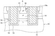
- the semiconductor device has a semiconductor substrate 10 constituting an N ⁇ -type drift layer 11.
- the semiconductor substrate 10 is formed of a silicon substrate.
- a P-type base layer 12 is formed on the drift layer 11 (that is, on the side of the surface 10 a of the semiconductor substrate 10).
- a plurality of trenches 13 are formed in the semiconductor substrate 10 so as to penetrate the base layer 12 and reach the drift layer 11.
- the base layer 12 is separated into a plurality.
- the plurality of trenches 13 are formed at equal intervals along one of the surface directions on one surface 10 a of the semiconductor substrate 10 (that is, the direction perpendicular to the sheet of FIG. It is done. That is, the trenches 13 are formed such that the intervals L between the adjacent trenches 13 are equal to each other.
- each trench 13 is formed such that the side surface is substantially parallel along the normal direction to the one surface 10 a of the semiconductor substrate 10.
- substantially parallel includes the case where the angle between the one surface 10 a of the semiconductor substrate 10 and the side surface of the trench 13 is about 85 °, in addition to the case of being completely parallel.
- a gate insulating film 14 is formed on the wall surface of each trench 13, and a gate electrode 15 is formed on the gate insulating film 14.
- the trench gate structure 16 is configured.
- the gate electrode 15 is formed to fill the inside of the trench 13.
- the gate insulating film 14 is formed of an oxide film, and is formed along the wall surface of the trench 13 with a uniform thickness of about 100 nm.
- the gate electrode 15 is made of polysilicon doped with an impurity.
- the gate electrode 15 is formed by depositing amorphous silicon by a CVD method and then heat treating it to crystallize the amorphous silicon into polysilicon, and the grain size of polysilicon is 50 to 1000 nm. There is.
- the impurity concentration of the N + -type emitter region 17 higher than that of the drift layer 11 and the base layer 12 is higher.
- P + -type contact regions 18 are respectively formed. Specifically, emitter region 17 is formed to terminate in base layer 12 and to be in contact with the side surface of trench 13. Further, the contact region 18 is formed to terminate in the base layer 12 in the same manner as the emitter region 17.
- emitter region 17 extends in a rod shape along the longitudinal direction of trench 13 so as to be in contact with the side surface of trench 13 in the region between trenches 13 and terminates inside the tip of trench 13 It is done. Further, the contact region 18 is sandwiched between the two emitter regions 17 and extends in a rod-like shape along the longitudinal direction of the trench 13 (that is, the emitter region 17).
- the contact region 18 of the present embodiment is formed deeper than the emitter region 17 with reference to the one surface 10 a of the semiconductor substrate 10.
- An interlayer insulating film 19 made of BPSG (abbreviation of Boron Phosphorus Silicon Glass) or the like is formed on one surface 10 a of the semiconductor substrate 10. Then, on the interlayer insulating film 19, an emitter electrode 20 electrically connected to the emitter region 17 and the contact region 18 (that is, the base layer 12) through the contact holes 19 a formed in the interlayer insulating film 19 is formed. It is done. In the present embodiment, the emitter electrode 20 corresponds to the first electrode.
- An N-type field stop layer (hereinafter referred to as “FS”) having an impurity concentration higher than that of the drift layer 11 on the opposite side of the drift layer 11 to the base layer 12 side (ie, the other surface 10 b side of the semiconductor substrate 10).
- a layer 21 is formed.
- this FS layer 21 is not necessarily required, the performance of withstand voltage and steady loss can be improved by preventing the spread of the depletion layer, and the injection amount of holes injected from the other surface 10b side of the semiconductor substrate 10 Prepared to control the
- a P-type collector layer 22 is formed on the opposite side to the drift layer 11 with the FS layer 21 interposed therebetween, and the collector layer 22 is electrically connected to the collector layer 22 (that is, the other surface 10b of the semiconductor substrate 10).
- Collector electrodes 23 connected to each other are formed. In the present embodiment, the collector electrode 23 corresponds to the second electrode.
- N-type, N + -type and N -- type correspond to the first conductivity type
- P-type and P + -type correspond to the second conductivity type.
- the semiconductor substrate 10 is configured to include the collector layer 22, the FS layer 21, the drift layer 11, the base layer 12, the emitter region 17, and the contact region 18.
- the above is the basic configuration of the semiconductor device in this embodiment. Next, the basic operation of the semiconductor device will be described.
- the emitter electrode 20 is grounded and a positive voltage is applied to the collector electrode 23. Then, a predetermined voltage is applied to the gate electrode 15 from a gate control circuit (not shown) so that the gate potential is equal to or higher than the threshold voltage Vth of the insulating gate structure.
- a gate control circuit not shown
- an N-type inversion layer i.e., a channel
- electrons are supplied from the emitter electrode 20 to the drift layer 11 through the emitter region 17 and the inversion layer.
- holes are supplied from the collector electrode 23 to the drift layer 11 through the collector layer 22. Then, in the semiconductor device, due to the conductivity modulation, the resistance value of the drift layer 11 is lowered to be turned on.
- a predetermined voltage for example, 0 V
- a gate control circuit not shown
- the inversion layer formed in the portion of base layer 12 in contact with trench 13 disappears, and electrons are not supplied from emitter electrode 20 and holes are not supplied from collector electrode 23. , Will be off.
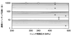
- the stress around the trench means the stress generated when forming the gate electrode 15 as described above, but means the maximum stress among the stresses generated around the trench 13 doing.
- the stress around the trench in FIG. 2 is the maximum stress among the stress in the center of the semiconductor device, the trench 13 at the outer edge, the trench 13 between the center and the outer edge, etc. It shows the stress. That is, the stress around the trench in FIG. 2 indicates the maximum stress among the stresses around the trench 13 in the semiconductor device.
- the stress generated in the periphery of the trench 13 is in the region between the adjacent trenches 13 because the stress caused by each gate electrode 15 disposed in the adjacent trench 13 is applied together. The predetermined part of the area in between is the largest.
- the stress around the trench in FIG. 2 is a value analyzed by the EBSD (abbreviation of Electron Back Scatter Diffraction) method.
- the number of continuous switchings in FIG. 2 is one switching from turning off the semiconductor device to turning on the semiconductor device and turning the semiconductor device from the on state to the off state.
- the semiconductor device of the present embodiment is configured such that the stress around the trench is 340 MPa or less.
- FIG. 2 shows that the thickness of the semiconductor substrate 10 is 80 ⁇ m, the stress around the trench does not change even if the thickness of the semiconductor substrate 10 and the impurity concentration of each region are changed. That is, regardless of the thickness of the semiconductor substrate 10 and the impurity concentration of each region, destruction of the semiconductor device is suppressed if the stress around the trench is 340 MPa or less.
- the stress around the trench is due to the polysilicon constituting the gate electrode 15 as described above. More specifically, the trench ambient stress is due to thermal contraction during and after crystallization from amorphous silicon to polysilicon. Therefore, the stress around the trench can be changed by adjusting the amount of polysilicon forming the gate electrode 15.
- FIG. 3 is a cross section in which the extending direction of the trench 13 is a normal direction, and corresponds to an enlarged view around the trench gate structure 16 in FIG. Then, in the region from one surface 10a of semiconductor substrate 10 to the bottom of trench gate structure 16 in this cross section, the center of trench gate structure 16 to the center of trench gate structure 16 located next to the other across contact region 18 Assume that it is a one-cell area A.
- a region surrounded by one central axis of the adjacent trench gate structure 16 and the other central axis is one cell Region A That is, in the region from one surface 10a of semiconductor substrate 10 to the bottom of trench gate structure 16 in this cross section, it passes through the centers of adjacent trench gate structures 16 along the normal direction to one surface 10a of semiconductor substrate 10.
- An area surrounded by two virtual lines is referred to as one cell area A.
- a region surrounded by a dotted line is a one-cell region A.
- the bottom portion of the trench 13 is the portion farthest from the one surface 10 a of the semiconductor substrate 10 and is the bottom surface of the trench 13 in FIG. 3.
- the present inventors investigate based on the volume ratio of the gate electrode 15 (that is, polysilicon) per cell area A (hereinafter, also simply referred to as the volume ratio of the gate electrode 15), and the following results I got That is, as shown in FIG. 4, when the volume ratio of the gate electrode 15 is 41.5% or less, it was found that the stress around the trench was 340 MPa or less.
- the volume ratio of the gate electrode 15 is 41.5% or less.
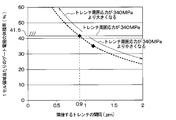
- the total volume of the one cell region A may be increased by widening the interval L between the adjacent trenches 13. That is, in the present embodiment, by setting the distance L between the adjacent trenches 13 to 0.9 ⁇ m or more, the stress around the trench can be set to 340 MPa or less.
- the semiconductor device when the semiconductor device is in the on state, holes supplied to the drift layer 11 are more easily released to the base layer 12 as the distance L between the adjacent trenches 13 is increased.
- the on voltage increases.
- the semiconductor device in which the IGBT having the trench gate structure 16 as in this embodiment is formed it is currently desired that the on voltage be 0.9 V or less.
- the rate of change of the on voltage in the range where the distance 13 between adjacent trenches is wider than 1.3 ⁇ m is smaller than the rate of change of the on voltage in the range where the distance between adjacent trenches 13 is 1.3 ⁇ m or less.
- the distance between the adjacent trenches 13 when the distance between the adjacent trenches 13 is 1.3 ⁇ m or less, the on-state voltage becomes steep as the distance between the adjacent trenches becomes narrow. Therefore, in the present embodiment, the distance between adjacent trenches is 1.3 ⁇ m or less.
- the distance L between the adjacent trenches 13 means the narrowest part of the adjacent trenches 13.
- the volume ratio of the gate electrode 15 per cell area A is set to 41.5% or less so that the stress around the trench is 340 MPa or less. Therefore, destruction of the semiconductor device can be suppressed.
- the distance L between the adjacent trenches 13 is set to 1.3 ⁇ m or less. Therefore, it is possible to suppress the destruction of the semiconductor device while suppressing the increase of the on voltage.
- the present embodiment is the same as the first embodiment except that the configuration of the trench gate structure 16 is different from the first embodiment, and the other parts are the same as the first embodiment, and thus the description thereof is omitted here.
- the trench 13 is configured such that the first trench 13a located on the opening side and the second trench 13b located on the bottom side are in communication.
- the first trench 13 a is formed in the base layer 12, and the second trench 13 b reaches the drift layer 11 from near the interface between the base layer 12 and the drift layer 11 in the base layer 12. Is formed. That is, the second trench 13 b of the present embodiment is formed across the base layer 12 and the drift layer 11.
- the second trench 13b is substantially circular in shape with a portion in which the distance between the facing side surfaces is longer than the distance between the facing side surfaces of the first trench 13a in the cross section in FIG. That is, the trench 13 has a so-called wedge shape in the cross section in FIG.
- interval of the side which opposes is the length of the paper surface left-right direction in FIG. Further, in the present embodiment, since the spacing L between the adjacent trenches 13 is the spacing of the narrowest portion among the spacings of the neighboring trenches 13, the spacing of the narrowest portion among the spacings of the adjacent second trenches 13b. It becomes.
- the gate electrode 15 is formed on the wall surface of the trench 13 via the gate insulating film 14 so that the air gap 24 is formed inside.
- the gate electrode 15 is formed such that the air gap 24 is formed in the second trench 13 b.
- FIG. 7 is a cross section in which the extending direction of the trench 13 is a normal direction, and corresponds to an enlarged view around the trench gate structure 16 in FIG.
- one cell region A is a region surrounded by a dotted line in the figure. Includes the air gap 24.
- the stress at the time of forming the gate electrode 15 is relieved by the air gap 24. Therefore, in the present embodiment, as shown in FIG. 8, for example, when the volume ratio of the gate electrode 15 is 41.5%, the distance L between the adjacent trenches 13 may be about 0.6 ⁇ m.
- the distance L between the trenches 13 can be made shorter than in the first embodiment. Therefore, when the semiconductor device is in the on state, holes supplied to the drift layer 11 can be made difficult to escape through the base layer 12. That is, according to the present embodiment, it is possible to further reduce the on-voltage while suppressing the destruction of the semiconductor device.
- FIG. 8 is a simulation result when the volume ratio of the air gaps 24 per one cell region A is 8%. Therefore, for example, when the volume ratio of the gate electrode 15 is 41.5%, when the volume ratio of the air gaps 24 per cell area A is made larger than 8%, the distance L between the adjacent trenches 13 is further increased. It becomes short. On the other hand, in the case where the volume ratio of the gate electrode 15 is 41.5%, when the volume ratio of the air gaps 24 per cell area A is made smaller than 8%, the distance L between the adjacent trenches 13 becomes wide.
- the semiconductor substrate 10 in which the base layer 12 is formed on the drift layer 11 is prepared, and anisotropic etching such as reactive ion etching is performed to form the first trench 13 a.
- anisotropic etching such as reactive ion etching is performed to form the first trench 13 a.
- a mask for protecting the side surface of the first trench 13a is formed, and isotropic etching is performed on the bottom of the first trench 13a.
- a second trench 13b is formed which has a portion in which the distance between the opposite side surfaces is longer than the distance between the opposite side surfaces of the first trench 13a, and which is in communication with the first trench 13a.
- the gate insulating film 14 is formed by the CVD method, thermal oxidation or the like. Then, amorphous silicon is deposited on the gate insulating film 14 by the CVD method or the like, and then heat treatment is performed to crystallize the amorphous silicon into polysilicon to form the gate electrode 15.
- amorphous silicon is deposited by the CVD method, amorphous silicon is deposited almost uniformly on the gate insulating film 14. Therefore, when amorphous silicon is deposited by the CVD method, the first trench 13a is buried before the inside of the second trench 13b is completely buried, and the air gap 24 is formed in the second trench 13b.
- the air gap 24 is formed inside the gate electrode 15, and the stress when forming the gate electrode 15 is relaxed by the air gap 24. Therefore, for example, when the volume ratio of the gate electrode 15 is 41.5%, the distance L between the adjacent trenches 13 can be shortened as compared with the first embodiment. Therefore, the breakdown of the semiconductor device can be suppressed while suppressing the increase of the on voltage.
- the first conductivity type is N-type and the second conductivity type is P-type
- the first conductivity type is P-type
- the second conductivity type is N-type
- the following configuration may be employed in order to set the volume ratio of the gate electrode 15 to 41.5% or less while setting the distance L between the adjacent trenches 13 to less than 0.9 ⁇ m.
- the gate electrode 15 is formed along the wall surface of the trench 13, and the embedded film 25 is embedded inside the gate electrode 15, so that the volume ratio of the gate electrode 15 is 41.5%. It is good also as the following.
- the embedded film 25 is formed, for example, by depositing an oxide film by the CVD method or the like.
- the volume ratio of the gate electrode 15 may be 41.5% or less by thickening a portion of the gate insulating film 14 disposed on the bottom side of the trench 13. In the case of such a configuration, concentration of the electric field at the bottom of the trench 13 can also be suppressed.
- the buried film 26 may be formed on the side of the opening of the trench 13. That is, since the gate electrode 15 may be formed in a portion in contact with the base layer 12 via the gate insulating film 14, the gate electrode 15 is formed in the portion opposite to the emitter region 17 with the gate insulating film 14 interposed therebetween. You do not have to. Therefore, the volume ratio of the gate electrode 15 may be reduced by forming the buried film 26 on the opposite side to the emitter region 17 with the gate insulating film 14 interposed therebetween.
- the embedded film 26 is formed, for example, by depositing an oxide film by the CVD method or the like.
- each configuration may be combined respectively.
- the configuration of FIGS. 9 and 10 may be combined, and the portion of the gate insulating film 14 disposed on the bottom side of the trench 13 may be thickened while the embedded film 25 is disposed.
- the configuration of FIGS. 9 and 11 may be combined to include both the buried film 25 and the buried film 26.
- the configuration of FIGS. 10 and 11 may be combined to include the buried film 26 while thickening the portion of the gate insulating film 14 disposed on the bottom side of the trench 13. Then, all the configurations shown in FIGS. 9 to 11 may be combined to make the portion of the gate insulating film 14 disposed on the bottom side of the trench 13 thicker while providing the embedded film 25 and the embedded film 26.
- the semiconductor device may be a so-called RC (Reverse Conducting abbreviation) -IGBT in which an N-type cathode layer is formed together with the collector layer 22 on the other surface 10b side of the semiconductor substrate 10. .
- RC Reverse Conducting abbreviation
- the plurality of trenches 13 may have different spacings L between adjacent trenches. Even with such a configuration, the same effect as described above can be obtained as long as the stress that is the largest among the stresses around the trench is 340 MPa or less.
Landscapes
- Electrodes Of Semiconductors (AREA)
- Chemical & Material Sciences (AREA)
- Engineering & Computer Science (AREA)
- Materials Engineering (AREA)
- Nanotechnology (AREA)
Priority Applications (2)
| Application Number | Priority Date | Filing Date | Title |
|---|---|---|---|
| CN201880071034.6A CN111295765B (zh) | 2017-11-03 | 2018-11-01 | 半导体装置 |
| US16/862,790 US11508836B2 (en) | 2017-11-03 | 2020-04-30 | Semiconductor device including trench gate structure with specific volume ratio of gate electrodes |
Applications Claiming Priority (2)
| Application Number | Priority Date | Filing Date | Title |
|---|---|---|---|
| JP2017213329A JP7009933B2 (ja) | 2017-11-03 | 2017-11-03 | 半導体装置 |
| JP2017-213329 | 2017-11-03 |
Related Child Applications (1)
| Application Number | Title | Priority Date | Filing Date |
|---|---|---|---|
| US16/862,790 Continuation US11508836B2 (en) | 2017-11-03 | 2020-04-30 | Semiconductor device including trench gate structure with specific volume ratio of gate electrodes |
Publications (1)
| Publication Number | Publication Date |
|---|---|
| WO2019088241A1 true WO2019088241A1 (ja) | 2019-05-09 |
Family
ID=66333276
Family Applications (1)
| Application Number | Title | Priority Date | Filing Date |
|---|---|---|---|
| PCT/JP2018/040772 Ceased WO2019088241A1 (ja) | 2017-11-03 | 2018-11-01 | 半導体装置 |
Country Status (4)
| Country | Link |
|---|---|
| US (1) | US11508836B2 (https=) |
| JP (1) | JP7009933B2 (https=) |
| CN (1) | CN111295765B (https=) |
| WO (1) | WO2019088241A1 (https=) |
Families Citing this family (1)
| Publication number | Priority date | Publication date | Assignee | Title |
|---|---|---|---|---|
| US20250142878A1 (en) * | 2023-10-25 | 2025-05-01 | Hon Young Semiconductor Corporation | Semiconductor device and manufacturing method thereof |
Citations (5)
| Publication number | Priority date | Publication date | Assignee | Title |
|---|---|---|---|---|
| JP2006114853A (ja) * | 2004-10-18 | 2006-04-27 | Toshiba Corp | 半導体装置及びその製造方法 |
| JP2007088010A (ja) * | 2005-09-20 | 2007-04-05 | Denso Corp | 半導体装置およびその製造方法 |
| JP2013251397A (ja) * | 2012-05-31 | 2013-12-12 | Denso Corp | 半導体装置 |
| WO2015019862A1 (ja) * | 2013-08-06 | 2015-02-12 | 富士電機株式会社 | トレンチゲートmos型半導体装置およびその製造方法 |
| JP2015213163A (ja) * | 2014-04-15 | 2015-11-26 | ローム株式会社 | 半導体装置および半導体装置の製造方法 |
Family Cites Families (11)
| Publication number | Priority date | Publication date | Assignee | Title |
|---|---|---|---|---|
| JP2874062B2 (ja) * | 1991-02-25 | 1999-03-24 | 松下電子工業株式会社 | 薄膜トランジスタの製造方法 |
| TW442972B (en) * | 1999-10-01 | 2001-06-23 | Anpec Electronics Corp | Fabricating method of trench-type gate power metal oxide semiconductor field effect transistor |
| US7217950B2 (en) * | 2002-10-11 | 2007-05-15 | Nissan Motor Co., Ltd. | Insulated gate tunnel-injection device having heterojunction and method for manufacturing the same |
| JP4534500B2 (ja) * | 2003-05-14 | 2010-09-01 | 株式会社デンソー | 半導体装置の製造方法 |
| JP2007005723A (ja) * | 2005-06-27 | 2007-01-11 | Toshiba Corp | 半導体装置 |
| JP2007043123A (ja) | 2005-07-01 | 2007-02-15 | Toshiba Corp | 半導体装置 |
| JP5609939B2 (ja) * | 2011-09-27 | 2014-10-22 | 株式会社デンソー | 半導体装置 |
| JP6459791B2 (ja) * | 2014-07-14 | 2019-01-30 | 株式会社デンソー | 半導体装置およびその製造方法 |
| JP2014232895A (ja) | 2014-09-11 | 2014-12-11 | 株式会社村田製作所 | 積層セラミックコンデンサ |
| KR102509260B1 (ko) * | 2015-11-20 | 2023-03-14 | 삼성디스플레이 주식회사 | 실리콘 연마 슬러리, 다결정 실리콘의 연마방법 및 박막 트랜지스터 기판의 제조방법 |
| US10643852B2 (en) * | 2016-09-30 | 2020-05-05 | Semiconductor Components Industries, Llc | Process of forming an electronic device including exposing a substrate to an oxidizing ambient |
-
2017
- 2017-11-03 JP JP2017213329A patent/JP7009933B2/ja active Active
-
2018
- 2018-11-01 WO PCT/JP2018/040772 patent/WO2019088241A1/ja not_active Ceased
- 2018-11-01 CN CN201880071034.6A patent/CN111295765B/zh active Active
-
2020
- 2020-04-30 US US16/862,790 patent/US11508836B2/en active Active
Patent Citations (5)
| Publication number | Priority date | Publication date | Assignee | Title |
|---|---|---|---|---|
| JP2006114853A (ja) * | 2004-10-18 | 2006-04-27 | Toshiba Corp | 半導体装置及びその製造方法 |
| JP2007088010A (ja) * | 2005-09-20 | 2007-04-05 | Denso Corp | 半導体装置およびその製造方法 |
| JP2013251397A (ja) * | 2012-05-31 | 2013-12-12 | Denso Corp | 半導体装置 |
| WO2015019862A1 (ja) * | 2013-08-06 | 2015-02-12 | 富士電機株式会社 | トレンチゲートmos型半導体装置およびその製造方法 |
| JP2015213163A (ja) * | 2014-04-15 | 2015-11-26 | ローム株式会社 | 半導体装置および半導体装置の製造方法 |
Also Published As
| Publication number | Publication date |
|---|---|
| JP7009933B2 (ja) | 2022-01-26 |
| JP2019087591A (ja) | 2019-06-06 |
| CN111295765B (zh) | 2023-04-18 |
| US20200312986A1 (en) | 2020-10-01 |
| US11508836B2 (en) | 2022-11-22 |
| CN111295765A (zh) | 2020-06-16 |
Similar Documents
| Publication | Publication Date | Title |
|---|---|---|
| CN101401212B (zh) | 绝缘栅极型半导体器件及其制造方法 | |
| JP6021908B2 (ja) | 絶縁ゲート型バイポーラトランジスタ | |
| CN105027292B (zh) | 半导体装置以及半导体装置的制造方法 | |
| JP5482886B2 (ja) | 半導体装置 | |
| JP5985624B2 (ja) | 絶縁ゲート型トランジスタおよびその製造方法 | |
| JP6226786B2 (ja) | 半導体装置およびその製造方法 | |
| JP6807390B2 (ja) | 半導体装置およびその製造方法 | |
| JP5470826B2 (ja) | 半導体装置 | |
| JP7272775B2 (ja) | 絶縁ゲートバイポーラトランジスタ | |
| JP6509673B2 (ja) | 半導体装置 | |
| JP2015118966A (ja) | 半導体装置 | |
| WO2013080806A1 (ja) | 絶縁ゲート型半導体装置およびその製造方法 | |
| JP6471508B2 (ja) | 半導体装置 | |
| JP2008130775A (ja) | 半導体装置 | |
| JPH07115189A (ja) | 絶縁ゲート型バイポーラトランジスタ | |
| JPWO2019049572A1 (ja) | 炭化珪素半導体装置および炭化珪素半導体装置の製造方法 | |
| US10748988B2 (en) | Semiconductor device | |
| JP6681238B2 (ja) | 半導体装置および半導体装置の製造方法 | |
| TW201944596A (zh) | 功率半導體元件 | |
| WO2019088241A1 (ja) | 半導体装置 | |
| JP2006332199A (ja) | SiC半導体装置 | |
| JP6771433B2 (ja) | 半導体装置 | |
| TW201608719A (zh) | 半導體裝置 | |
| JP2014225693A (ja) | 半導体装置およびその製造方法 | |
| US20150364585A1 (en) | Power semiconductor device |
Legal Events
| Date | Code | Title | Description |
|---|---|---|---|
| 121 | Ep: the epo has been informed by wipo that ep was designated in this application |
Ref document number: 18874128 Country of ref document: EP Kind code of ref document: A1 |
|
| NENP | Non-entry into the national phase |
Ref country code: DE |
|
| 122 | Ep: pct application non-entry in european phase |
Ref document number: 18874128 Country of ref document: EP Kind code of ref document: A1 |